Embed Size (px)
Citation preview

© IMEC 2010 / CONFIDENTIAL
Resistive switching materials and devices for future memory applications
Dirk Wouters
Principal Scientist Memory
Tutorial SISC San Diego, 5 December 2012
43rd IEEE Semiconductor
Interface Specialists
Conference
IMEC 2012

© IMEC 2010 / CONFIDENTIAL
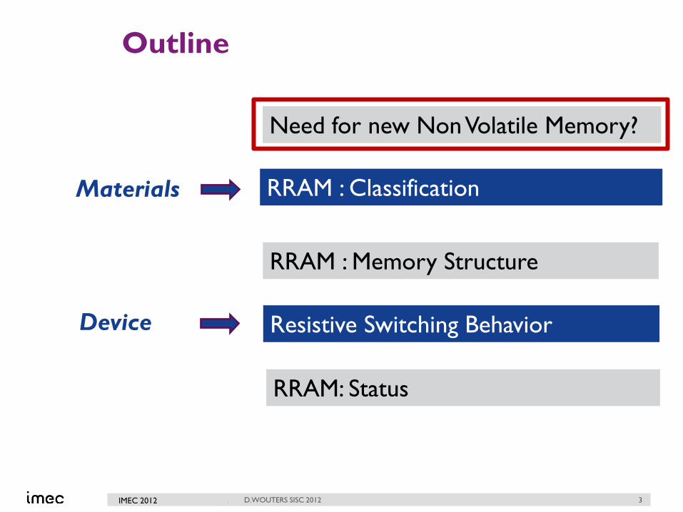
Outline
D.WOUTERS SISC 2012 2
RRAM : Classification
Need for new Non Volatile Memory?
RRAM : Memory Structure
Resistive Switching Behavior
RRAM: Status
Materials
Device
IMEC 2012
© IMEC 2010 / CONFIDENTIAL
Outline
D.WOUTERS SISC 2012 3
RRAM : Classification
Need for new Non Volatile Memory?
RRAM : Memory Structure
Resistive Switching Behavior
RRAM: Status
Materials
Device
IMEC 2012

© IMEC 2010 / CONFIDENTIAL
Need for new Non-Volatile Memory ?
▸ Growing NVM market
▸ Flash scaling issues
▸ New opportunities?
D.WOUTERS SISC 2012 4 IMEC 2012

© IMEC 2010 / CONFIDENTIAL D.WOUTERS SISC 2012
NVM market is growing exponentially
5 IMEC 2012

© IMEC 2010 / CONFIDENTIAL D.WOUTERS SISC 2012
Smartphones Tablets
PC SSD Enterprise SSD
NVM Growth drivers
Slide courtesy G.Jurczak, imec 6 IMEC 2012

© IMEC 2010 / CONFIDENTIAL
Main Non-Volatile Memory = FLASH
▸ Operation based on floating gate transistor
- threshold voltage is shifted by putting (PROGRAM) or
removing (ERASE) charge from the floating gate (by hot
carrier injection or tunneling)
- READ-OUT by selecting element and current sensing
- mainstream nonvolatile memory technology of today due to
high CMOS compatibility and high quality of silicon dioxide
▸ NOR and NAND type
D.WOUTERS SISC 2012
S D
Gate
Floating Gate
VG
ID
ID
OFF ON
VT1 < VGprobe < VT2 VG
ID
ID
OFF ON
VT1 < VGprobe < VT2
7 IMEC 2012

© IMEC 2010 / CONFIDENTIAL 8
Cell configurations : NOR
▸ NOR : ½ drain (BL) contact/cell
- fast random access, fast programming, robust code (Cellular)
- Larger cell size ~10F2
Source
Bit line
Word line
Source
Bit line
Word line
basic layout y-pitch cross-sectionx
y
x-pitch cross-sectionarray equivalent circuit
Source
Bit line
Word line
Source
Bit line
Word line
basic layout y-pitch cross-sectionx
y
x
y
x-pitch cross-sectionarray equivalent circuit
WL1
BL
Vpp=12V
5V
WL2 0
D.WOUTERS SISC 2012 IMEC 2012

© IMEC 2010 / CONFIDENTIAL 9
Cell configurations : NAND
▸ NAND : contactless:
- slow access (but fast burst read), low program power data
- Smallest cell size : ~4F2
Source
Bit line
W .L.
Bit line sel.
B it line sel.
Source
Bit line
W .L.
Bit line sel.
B it line sel.
basic layout y-pitch cross-sectionx
y
x-pitch cross-sectionarray equivalent circuitSource
Bit line
W .L.
Bit line sel.
B it line sel.
Source
Bit line
W .L.
Bit line sel.
B it line sel.
basic layout y-pitch cross-sectionx
y
x
y
x-pitch cross-sectionarray equivalent circuit
WL
BL
Vselect
Vpp= 18V
0
0
D.WOUTERS SISC 2012 IMEC 2012

© IMEC 2010 / CONFIDENTIAL
NAND = minimal cell size memory !!!
NAND Flash is TRUE Cross-Point (XP)
memory !
D.WOUTERS SISC 2012 10
Cell size = 4F2
IMEC 2012

© IMEC 2010 / CONFIDENTIAL 11
Success of FLASH = small 1T cell &
scalability
From IMST Whitebook 2007
D.WOUTERS SISC 2012 IMEC 2012
© IMEC 2010 / CONFIDENTIAL
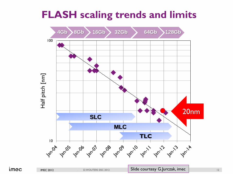
FLASH scaling trends and limits
10
100 H
alf pitch
[nm
]
128Gb 64Gb 32Gb 16Gb 8Gb 4Gb
20nm
D.WOUTERS SISC 2012 Slide courtesy G.Jurczak, imec
SLC
MLC
TLC
12 IMEC 2012

© IMEC 2010 / CONFIDENTIAL
NAND Flash scaling issues
D.WOUTERS SISC 2012 13
Scaling limitations
▸ Reduced FG coupling of scaled device
▸ Limit of tunnel ox scaling - No further voltage scaling
▸ Electrostatic interaction between
neighboring cells
▸ Dense patterning requirements
ahead of advanced litho - Dual patterning developments
IMEC 2012

© IMEC 2010 / CONFIDENTIAL
Charge = quantized !
D.WOUTERS SISC 2012 14
Flash scalability based on charge density <> total charge DRAM
Hower, ultimately charge is made up from electrons...
▸ At 20nm, less than 100 electrons are present on the FG for Vt=1
▸ If 20% charge loss is the spec, we talk about ~10 electrons…
▸ for 10 yrs retention, Ileak<<1e/yr…
K.Prall, NVSMW, 2007
IMEC 2012
Scaling advantage of new non-charge based memories concepts ?

© IMEC 2010 / CONFIDENTIAL
Flash explores other scaling routes
▸ Multi-level programming
- 2-3-4 bits/cell
- Currently implemented
▸ Planar 3D Flash
- Effective cell area : divided by number of layers!
- Cost-effective integration to stack bits vertically
- Different 3D concepts (BICS, TCAT,VSAT )
- Not (yet) in production
D.WOUTERS SISC 2012 15 Bit Cost Scaling FLASH, Toshiba IEDM 2007 IMEC 2012

© IMEC 2010 / CONFIDENTIAL
Flash BIT scaling
D.WOUTERS SISC 2012 16
Bit S
ize (
mm
2)
Year of Production
1
0.1
0.01
0.001
0.0001
NAND
6T-SRAM
DRAM
2b MLC-NAND
2002 2004 2006 2008 2010 2012 2014 2016
3D-NAND
Same bit size for
larger node
After H.E. Maes and J. Van Houdt,
keynote @IEEE NVSMW 2003
Any new technology competing with Flash should enable all scaling routes
right metric
= F2/bit
IMEC 2012

© IMEC 2010 / CONFIDENTIAL
Performance degradation of scaled Flash
NA
ND
Perf
orm
ance
& R
elia
bili
ty
time
Consumer
electronics
Mobile
Storage
Consumer
SSD
Enterprise
storage
Perf
orm
ance
gap
D.WOUTERS SISC 2012
Slide courtesy G.Jurczak, imec
With increasing density and MLC,
NAND performance degrades
17 IMEC 2012

© IMEC 2010 / CONFIDENTIAL
Latency GAP between DRAM and NAND
Opportunity for new class of (NV) memories :
Storage Class Memory (SCM)
~ “performant FLASH”
D.WOUTERS SISC 2012 18 IMEC 2012

© IMEC 2010 / CONFIDENTIAL
DIFFERENT CLASSES OF SCM
Storage type SCM : (close to HDD)
▸ a high-performance solid-state drive, accessed
by the system I/O controller much like an HDD
Memory type SCM: (close to DRAM)
▸ should offer a read/write latency of less than 1
ms. These specifications would allow it to remain
synchronous with a memory system, allowing direct
connection from a memory controller and bypassing
the inefficiencies of access through the I/O controller.
D.WOUTERS SISC 2012 19
ERD ITRS meeting Potsdam 2011
IMEC 2012

© IMEC 2010 / CONFIDENTIAL
Outline
D.WOUTERS SISC 2012 20
RRAM : Classification
Need for new Non Volatile Memory?
RRAM : Memory Structure
RRAM: Status
Materials
Device
IMEC 2012
Resistive Switching Behavior

© IMEC 2010 / CONFIDENTIAL
RRAM : classification & materials
▸ RRAM : general definitions & history...
▸ Classification
▸ Filamentary switching
- Properties of filamentary switching
- Thermo-chemical RRAM
- Bipolar “oxygen vacancy drift” RRAM
- Electro-chemical CBRAM
▸ Interfacial switching
D.WOUTERS SISC 2012 21 IMEC 2012
© IMEC 2010 / CONFIDENTIAL
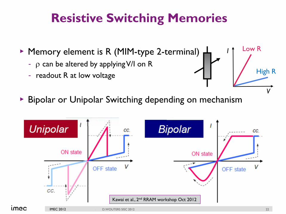
Resistive Switching Memories
▸ Memory element is R (MIM-type 2-terminal)
- r can be altered by applying V/I on R
- readout R at low voltage
▸ Bipolar or Unipolar Switching depending on mechanism
D.WOUTERS SISC 2012
Kawai et al., 2nd RRAM workshop Oct 2012
V
I Low R
High R
22 IMEC 2012

© IMEC 2010 / CONFIDENTIAL
Resistive Switching Memories
▸ A 2-terminal resistor element with electrically alterable
resistivity
- typically a low and high conductive state, although (controllable)
multi conductive states would be an asset (MLC)
- focus on programming with an electrical signal (e.g. not magnetic)
▸ Focus on non-volatile resistivity change
- Different from Ovonic switching
(electronic switching from low to high-conductive state,
but requiring a hold current to remain in high-conductive state),
and also of typical Mott transition element (as VO2)
▸ Focus on elements that can switch repeatedly from low to
high conductive state.
- Different from typical Fuse or anti-Fuse element (limited application
to OTP)
D.WOUTERS SISC 2012 23 IMEC 2012

© IMEC 2010 / CONFIDENTIAL
The Time-Voltage Dilemma
Fast programming
▸ At ~1V, need programming in ~10nsec
Good retention
▸ At ~0.1V, need stable read for ~ 10 years
D.WOUTERS SISC 2012 24
Need operation mechanism with extreme non-linear behavior:
>15 orders of magnitude in time over 1 decade in voltage
R.Waser (RWTH/Julich)
IMEC 2012
How can we make a 2-terminal NVM ?

© IMEC 2010 / CONFIDENTIAL 25
Discovery resistive switching in oxides : 1960’s !
Vol 11, May 1964, p. 243 Au/SiO/Au structure
SiO !
D.WOUTERS SISC 2012 25 IMEC 2012

© IMEC 2010 / CONFIDENTIAL
Resistive switching effect in Transition Metal
Oxides
▸ First switching of NiO was already reported in 1964!
D.WOUTERS SISC 2012 27 IMEC 2012

© IMEC 2010 / CONFIDENTIAL
Whatever happened to….
▸ Resisitive switching memories based on these
concepts eventually never developed :
- problems of stability
- scaling questioned
- emergence & rapid successful development of Si-
based memories !
D.WOUTERS SISC 2012 28 IMEC 2012

© IMEC 2010 / CONFIDENTIAL
Recent surge of interest
5 important events that put oxide RRAM again in the
picture :
1. A.Beck, B.J.Bednorz et al, IBM Zurich, APL 2000
2. W.Zhuang et al, Sharp/Univ Houston, IEDM 2002
3. I.G.Baek et al., Samsung, IEDM 2004
4. D.B.Strukov et al, HP labs, Nature 2008
5. H.Y.Lee et al, ITRI, IEDM, Tech. Dig., p. 297 2008
29 IMEC 2012

© IMEC 2010 / CONFIDENTIAL
1. A.Beck, B.J.Bednorz et al, IBM Zurich, APL
2000
• Thin oxide films for memory are back !
D.WOUTERS SISC 2012 30 IMEC 2012

© IMEC 2010 / CONFIDENTIAL
2. W.Zhuang et al, Sharp/Univ Houston, IEDM 2002
• coined the term RRAM
• realization 1D1R array
Principle on bulk crystals published by A.Asamitsu et al., Nature, 1997
D.WOUTERS SISC 2012 31 IMEC 2012

© IMEC 2010 / CONFIDENTIAL
3. I.G.Baek et al., Samsung, IEDM 2004
IEDM 2004
• 1st advanced work (integrated device) with simple binary oxide (NiO)
• Coined the term OxRRAM (switching in TMO)
D.WOUTERS SISC 2012 32 IMEC 2012

© IMEC 2010 / CONFIDENTIAL
4. D.B.Strukov et al.,HP labs,Nature2008
• Memristor concept applied to RRAM
• Triggered a lot of interest, especially in EE (design) world
D.WOUTERS SISC 2012 33 IMEC 2012
© IMEC 2010 / CONFIDENTIAL
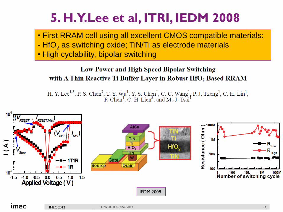
5. H.Y.Lee et al, ITRI, IEDM 2008
D.WOUTERS SISC 2012 34
• First RRAM cell using all excellent CMOS compatible materials:
- HfO2 as switching oxide; TiN/Ti as electrode materials
• High cyclability, bipolar switching
IEDM 2008
IMEC 2012

© IMEC 2010 / CONFIDENTIAL
RRAM : classification & materials
▸ RRAM : general definitions & history...
▸ Classification
▸ Filamentary switching
- Properties of filamentary switching
- Thermo-chemical RRAM
- Bipolar “oxygen vacancy drift” RRAM
- Electro-chemical CBRAM
▸ Interfacial switching
D.WOUTERS SISC 2012 35 IMEC 2012

© IMEC 2010 / CONFIDENTIAL
Taxonometry of Resistive Switching
Memories : based on Mechanism
Resistive Switching N
an
om
ech
an
ical
Mem
ory
N
an
om
ech
an
ical
Me
mo
ry
Na
no
me
ch
an
ical
Me
mo
ry
Ele
ctro
sta
tic
Effe
cts
E
lectro
sta
tic
Effe
cts
Ph
ase
Ch
an
ge
M
em
ory
Effe
ct
Ph
ase
Ch
an
ge
M
em
ory
Effe
ct
Effe
ct
Re
do
x - b
ase
d
Me
mo
ry E
ffect
Re
do
x - b
ase
d
Me
mo
ry E
ffect
Re
do
x - b
ase
d
Me
mo
ry E
ffect
Ele
ctro
chem
ical
Me
mo
ry E
ffect
Ele
ctro
chem
ical
Mem
ory
Effe
ct
Ele
ctro
chem
ical
Mem
ory
Effe
ct
Mo
lecu
lar
Sw
itch
ing E
ffects
M
ole
cu
lar
Sw
itch
ing E
ffects
M
ole
cu
lar
Sw
itch
ing E
ffects
Ma
gn
eto
resis
tive
Me
mo
ry E
ffects
M
ag
ne
tore
sis
tive
Mem
ory
Effe
cts
M
ag
ne
tore
sis
tive
Mem
ory
Effe
cts
Fe
rroe
lectric
T
unn
elin
g
Ferro
ele
ctric
T
unn
elin
g
Thermo - and electro - chemical switching
phenomena in oxides T
he
rmo
ch
em
ica
l M
em
ory
Effe
ct
Th
erm
och
em
ica
l M
em
ory
Effe
ct
Th
erm
och
em
ica
l M
em
ory
Effe
ct
Ele
ctro
sta
tic
Effe
cts
Ph
ase
Ch
an
ge
M
em
ory
Ferro
ele
ctric
T
unn
elin
g
Adapted from R.Waser, IEDM 2008
(Mott)
“ReRAM”
“MRAM” “PRAM” PCRAM MRAM
RRAM
D.WOUTERS SISC 2012 36 IMEC 2012

© IMEC 2010 / CONFIDENTIAL
Resistance Modulation Geometry
Electronic MIT
(Mott)
Electro- chemical
3D
Bulk Transition
Cation Source (Ag+, Cu+ or...)
Cu+
Ag+
BE
ME
TA
LIC
FIL
AM
EN
T
Schottky barrier
2D
Interfacial
TE
BE
MIT
TE
BE
exchange layer
O vacancy,...
perovskite
1D Filamentary
Phase change
Tunnel Magneto
resistance
Thermo- Chemical
Fuse/ antifuse
TE
BE
metaloxide
reduced
TE
BE
MIT
amorphous
Poly-
crystaline
TE
BE
MITTunnel barrier
Free layer
Pinned layer
UNIPOLAR BIPOLAR BIPOLAR BIPOLAR UNIPOLAR UNIPOLAR
RRAM D.WOUTERS SISC 2012
PCRAM MRAM ?
Oxygen vacancy migration
TE
BE
MIT
BIPOLAR
37 IMEC 2012

© IMEC 2010 / CONFIDENTIAL
RRAM : classification & materials
▸ RRAM : general definitions & history...
▸ Classification
▸ Filamentary switching - Properties of filamentary switching
- Thermo-chemical RRAM
- Bipolar “oxygen vacancy drift” RRAM
- Electro-chemical CBRAM
▸ Interfacial switching
D.WOUTERS SISC 2012 38 IMEC 2012

© IMEC 2010 / CONFIDENTIAL
1D Filamentary switching
D.WOUTERS SISC 2012 39
Electro- chemical
Cation Source (Ag+, Cu+ or...)
Cu+
Ag+
BE
ME
TA
LIC
FIL
AM
EN
T
1D Filamentary
Thermo- Chemical
Fuse/ antifuse
TE
BE
metaloxide
reduced
UNIPOLAR BIPOLAR
Oxygen vacancy migration
TE
BE
MIT
BIPOLAR
?
IMEC 2012

© IMEC 2010 / CONFIDENTIAL
Indications for filamentary switching
D.WOUTERS SISC 2012 40
R. Münstermann et al.,
PSS RRL4 (2010) 16-18
K. Szot, Phys. stat. sol. (RRL) 1, No. 2, R86–R88 (2007) / DOI 10.1002
IMEC 2012
From physico-chemical analysis

© IMEC 2010 / CONFIDENTIAL
Indications for filamentary switching
Electrical fingerprint from device characteristics
- Area (in)dependence of LRS/HRS and switching voltages
D.WOUTERS SISC 2012 41
F.Nardi et al, IEEE Trans. El.Dev. 59(9). 2661 (2012)
IMEC 2012

© IMEC 2010 / CONFIDENTIAL
Different steps in a filamentary
switching process
▸ Forming
▸ RESET
▸ SET
D.WOUTERS SISC 2012 42
Akihito Sawa, materialstoday, Vol11(6), 2008
1.E-09
1.E-07
1.E-05
1.E-03
0 0.5 1 1.5
forming
set
reset
Voltage
Cu
rren
t
real switching curves
L.Goux (imec), NiO/Ni RRAM cell
C.Cagli, IEDM 2008
IMEC 2012

© IMEC 2010 / CONFIDENTIAL
Forming: creating a conduction path by
“breakdown”
D.WOUTERS SISC 2012 43
NiO by MOCVD imec
0
1
2
3
4
5
6
7
8
0.0 5.0 10.0 15.0 20.0 25.0 30.0
Thickness (nm)
V f
orm
ing
(V
)
Similar to (soft) breakdown in dielectrics (defect &
percolation path generation)
Forming
voltage scales
with thickness
IMEC 2012

© IMEC 2010 / CONFIDENTIAL
Maximum current during Forming(/SET)
controls filament “Strength”
D.WOUTERS SISC 2012 44
Y.Satoet al, Trans.El.Dev. 2008 D.Ielmini et al, Trans.El.Dev. 58(12), p.4309, 2011
IMEC 2012
© IMEC 2010 / CONFIDENTIAL
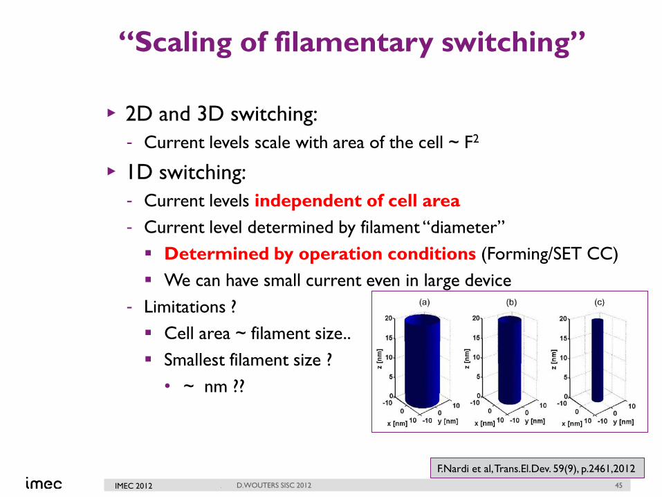
“Scaling of filamentary switching”
▸ 2D and 3D switching:
- Current levels scale with area of the cell ~ F2
▸ 1D switching:
- Current levels independent of cell area
- Current level determined by filament “diameter”
Determined by operation conditions (Forming/SET CC)
We can have small current even in large device
- Limitations ?
Cell area ~ filament size..
Smallest filament size ?
• ~ nm ??
D.WOUTERS SISC 2012 45
F.Nardi et al, Trans.El.Dev. 59(9), p.2461,2012
IMEC 2012

© IMEC 2010 / CONFIDENTIAL
Influence of spike currents
D.WOUTERS SISC 2012 46
Ireset=Icomp
Iset CC
Expected
Ireset
Cp
discharging
current
True Ireset
L.Goux et al, IEEE TED 2009 (sept 09)
IMEC 2012

© IMEC 2010 / CONFIDENTIAL
1T1R integrated teststructure for stable
current control
D.WOUTERS SISC 2012 47
Kinoshita et al, APL vol. 93
IMEC 2012

© IMEC 2010 / CONFIDENTIAL 48 2012 / imec
Intrinsic Forming voltage scaling
D.WOUTERS SISC 2012
B.Govoreanu, IEDM 2011
IMEC 2012

© IMEC 2010 / CONFIDENTIAL
Area dependence of Forming voltage
D.WOUTERS SISC 2012 49
1 2 3 4 5 6-10
-8
-6
-4
-2
0
2
Forming voltage, VF [V]
We
ibit,
ln(-
ln(1
-F))
Cell 1
Cell 2
Cell 3
Cell 4
1 2 3 4 5 6
Forming voltage, VF [V]
Cell 1
Cell 2
Cell 3
Cell 4
Cell 5
5 nm 10 nmNP P 5 nm
10 nm
1 2 3 4 5 6-10
-8
-6
-4
-2
0
2
Forming voltage, VF [V]
We
ibit,
ln(-
ln(1
-F))
Cell 1
Cell 2
Cell 3
Cell 4
1 2 3 4 5 6
Forming voltage, VF [V]
Cell 1
Cell 2
Cell 3
Cell 4
Cell 5
5 nm 10 nmNP P 5 nm
10 nm
B.Govoreanu, SSDM 2011
Due to defect distribution statistics
▸ Fitting single area-scaled Weibull plot
IMEC 2012

© IMEC 2010 / CONFIDENTIAL
Area dependence of Forming
Due to defect distribution statistics
▸ Difference between amorphous and crystalline
VFORMING : linked to different leakage current tails
D.WOUTERS SISC 2012
B.Govoreanu, IEDM 2011
50 IMEC 2012

© IMEC 2010 / CONFIDENTIAL
Switching during SET/RESET:
SET = Forming
D.WOUTERS SISC 2012 51
0
0.2
0.4
0.6
0.8
1
RE
Se
t vo
lta
ge
, V
S [
V]
1mm 100nm 10nm 10nmCell size
5nm HfOx10nm HfOx
10nm-size cells0
0.2
0.4
0.6
0.8
1
RE
Re
se
t vo
lta
ge
, V R
[V
]
1mm 100nm 10nm 10nmCell size
5nm HfOx10nm HfOx
10nm-size cells
B.Govoreanu, IEDM2011
Absence of oxide thickness effect on
VSET/RESET indicative of LOCAL
filament switching
IMEC 2012

© IMEC 2010 / CONFIDENTIAL
Forming free for thin films ?
▸ Linear scaling with
oxide thickness:
- Field driven
▸ Predicts “forming-
free” behavior if
tox<2.5 nm
- limitation ?
new filament creation
@ each Set ?
D.WOUTERS SISC 2012
B.Govoreanu et al, IEDM 2011
52 IMEC 2012

© IMEC 2010 / CONFIDENTIAL
Single or multiple filaments ?
D.WOUTERS SISC 2012 53
J.Y.Son, Y.-H.Shin, Appl.Phys.Lett. 2008,92,222106 R.Degraeve et al., IEDM 2010
Indications of multi-filaments? IMEC 2012

© IMEC 2010 / CONFIDENTIAL
“Forming” at lower voltage...
D.WOUTERS SISC 2012 54
R.Degraeve et al., IEDM 2010
BD theory predicts possible activation of new
filaments even at lower SET voltage..
IMEC 2012

© IMEC 2010 / CONFIDENTIAL
The winner takes it all ?
D.WOUTERS SISC 2012 55
Ch. Lenser et al., J. Appl. Phys. 111, 076101 (2012);
Most models assume
single filament
IMEC 2012

© IMEC 2010 / CONFIDENTIAL
RRAM : classification & materials
▸ RRAM : general definitions & some history...
▸ Classification
▸ Filamentary switching
- Properties of filamentary switching
- Thermo-chemical RRAM
- Bipolar “oxygen vacancy drift” RRAM
- Electro-chemical CBRAM
▸ Interfacial switching
D.WOUTERS SISC 2012 56 IMEC 2012

© IMEC 2010 / CONFIDENTIAL
Unipolar Switching OxRRAM :
“Thermo-Chemical Fuse/antifuse”
D.WOUTERS SISC 2012 57
Top Electrode
Bottom Electrode
NiO
Low R High R
Set state Reset state Conductive
filament (CF)
Material : Transition Metal-Oxides, e.g. NiO, HfO,..
1D Filamentary
Thermo- Chemical
Fuse/ antifuse
TE
BE
metaloxide
reduced
UNIPOLAR
IMEC 2012

© IMEC 2010 / CONFIDENTIAL
Role of oxygen / oxygen vacancy defects
in OxRRAM memories
▸ Filament switching involves oxygen transport
▸ Filament observations indicate local lower O concent
- Magnelli phase of Ti4O7 or Ti5O9 , essentially TiO2-x
Oxygen vacancy defects
D.WOUTERS SISC 2012 58
Szot et al., Nature materials (2006)
Bubbles < O2 released to the gas phase or adsorbed by the grainboundaries
of the Pt electrode
D. H. Kwon et al., Nature Nano technology(2010) IMEC 2012

© IMEC 2010 / CONFIDENTIAL
Oxygen vacancy filament conduction
▸ Oxygen vacancies influence conduction
- Electron hopping from one vacancy to another
- Act as local “doping” thermally activated conduction
- Create conductive defect band in Metal Oxide (e.g. at GB)
Metallic conduction
D.WOUTERS SISC 2012
S.Larentis et al,
Trans. El.Dev. 59(9), 2012, p. 2468 G.Bersuker et al.,
J. Appl. Phys. 110, 124518 (2011)
N.Xu et al,
VLSI Technology, 2008
59 IMEC 2012 IMEC 2012

© IMEC 2010 / CONFIDENTIAL
Why Transition Metal Oxides?
▸ Transition metals, have 2 or multiple oxidation states
▸ Transition metal oxides are good ionic conductors.
(Used in fuel cells for that reason)
D.WOUTERS SISC 2012 60
S.Muraoka et al., IEDM 2007
IMEC 2012

© IMEC 2010 / CONFIDENTIAL
Switching Process
▸ Forming creates filament consisting of oxygen vacancies
▸ RESET: local oxidation ; (Forming/)SET: local reduction
▸ How to explain process and unipolar character ?
D.WOUTERS SISC 2012 61
O2
O2
O2
O2
O2
O2
O2
O2
O2
O2
= oxygen vacancy
IMEC 2012

© IMEC 2010 / CONFIDENTIAL
Unipolar SET process
D.WOUTERS SISC 2012 62
Stage 1: high-field threshold switching high current path
Stage 2: high current also induces Joule heating
High Field + high T: damage MOx (bond breaking/reduction)
permanent conductive path
SET
C.Cagli et al, IEDM 2008
O2
O2
O2
O2
O2
IMEC 2012

© IMEC 2010 / CONFIDENTIAL
Unipolar RESET process
D.WOUTERS SISC 2012 63
RESE
T
High (ON) current induces high T by Joule heating
Thermal oxidation “dissolves” of the filament
M (conducting)+O MO (insulating)
U.Russo et al, IEDM 2007
O2
O2
O2
O2
O2
IMEC 2012

© IMEC 2010 / CONFIDENTIAL
Why unipolar ?
Non-directional mechanisms:
- temperature
- “BD” field
D.WOUTERS SISC 2012 64

© IMEC 2010 / CONFIDENTIAL
Anodic Oxidation @ “active” electrode
▸ Previous model does not take effect of electrodes
into account
▸ Actual switching requires “active” electrode
- Pt, Ni, ...
- Active electrode catalyses anodic oxidation reaction during
RESET
- Filament “rupture” at active electrode interface and not at
center as deduced from pure thermal simulations
D.WOUTERS SISC 2012 65
+ +
+
++
++ ++
+
+ +
++
+++
++
++ +
++
+
+
Ni or Pt
TiN
+ +
+
++
++ ++
+
+ +
++
+++
++
++ +
++
+
+
Ni or Pt
TiN
(a) (b) (c)
dx
Ni or Pt
NiO1-x
NiOdy dy
Ni or Pt
NiO1-x
NiO
(d)+VRESET+VRESET
+ +
+
++
++ ++
+
+ +
++
+++
++
++ +
++
+
+
Ni or Pt
TiN
+ +
+
++
++ ++
+
+ +
++
+++
++
++ +
++
+
+
Ni or Pt
TiN
(a) (b) (c)
dx
Ni or Pt
NiO1-x
NiOdy dy
Ni or Pt
NiO1-x
NiO
(d)+VRESET+VRESET
L.Goux et al,VLSI Technology 2011
IMEC 2012

© IMEC 2010 / CONFIDENTIAL
A-polar and Uni-polar switching
▸ Unipolar switching:
- SET and RESET at SAME polarity
- However, RESET needs specific
polarity due to anodic oxidation
▸ Apolar switching:
- Only in symmetric structure :
Active electrode as both bottom and top electrode
D.WOUTERS SISC 2012 66
A.Cagli et al, IEDM 2011
1.E-08
1.E-06
1.E-04
1.E-02
0 0.5 1
LRS
HRS
1 Voltage to Ni (V)
Cu
rre
nt (
A) 2
83
4 ...
0
5
10
0 20 40
~1.5MV/cm
tox (nm)
VF (V)
L.Goux et al,VLSI Technology 2011
IMEC 2012

© IMEC 2010 / CONFIDENTIAL
PRO/CON Unipolar switching
▸ Unipolar switching mechanism:
FORMING/SET : High Field activated reduction
RESET : High T induced local re-oxidation (Joule heating)
Oxygen diffuses “locally”
▸ High energy (thermal activated process, breakdown)
High V, I
Stronger filament “break” : higher R-window
▸ Loss of oxygen : diffusion is not very directional
Limited cyclability
▸ 1 voltage polarity :
use of simple DIODE as selector : 1D1R cell
D.WOUTERS SISC 2012 67 IMEC 2012

© IMEC 2010 / CONFIDENTIAL
State of the art.../1 typical results
D.WOUTERS SISC 2012 68
“High Performance Unipolar AlOy/HfOx/Ni based RRAM Compatible with Si Diodes for 3D Application”,
X.A. Tran, VLSI Technology 2011
IMEC 2012

© IMEC 2010 / CONFIDENTIAL
State of the art.../2. low current results
D.WOUTERS SISC 2012 69
Y.-H.Tseng et al, IEDM 2009
Low current but at expense
of window and extreme
poor cyclability
IMEC 2012

© IMEC 2010 / CONFIDENTIAL
NTHU/TSMC ISSCC 2012 1T1R
D.WOUTERS SISC 2012
Unipolar
NTHU/TSMC ISSCC 2012
70 IMEC 2012

© IMEC 2010 / CONFIDENTIAL
RRAM : classification & materials
▸ RRAM : general definitions & some history...
▸ Classification
▸ Filamentary switching
- Properties of filamentary switching
- Thermo-chemical RRAM
- Bipolar “oxygen vacancy drift” RRAM
- Electro-chemical CBRAM
▸ Interfacial switching
D.WOUTERS SISC 2012 71 IMEC 2012

© IMEC 2010 / CONFIDENTIAL
Bipolar Switching OxRRAM :
“Oxygen Vacancy Migration”
D.WOUTERS SISC 2012 72
1D Filamentary
Oxygen vacancy migration
TE
BE
MIT
BIPOLAR
Material : TMO’s , e.g. HfO,TiO,TaO..
H.Y.Lee et al, “Low Power
and High Speed Bipolar
Switching with A Thin
Reactive Ti Buffer Layer in
Robust HfO2 Based
RRAM”, IEDM, Tech. Dig.,
pp. 297, 2008
IMEC 2012

© IMEC 2010 / CONFIDENTIAL
Bipolar vs unipolar switching OxRRAM
▸ Same TMO-based RRAM cells ?
- Requirement for bipolar switching = asymmetric structure
▸ Type I : cells with one “active” electrode :
- Show both unipolar and bipolar switching
▸ Type II: cells with asymmetrically built-in oxygen
vacancies
- Cells show bipolar switching
Mechanism ?
▸ Focus here on HfO2 based RRAM
D.WOUTERS SISC 2012 73
TE
BE
HfO2
IMEC 2012
© IMEC 2010 / CONFIDENTIAL
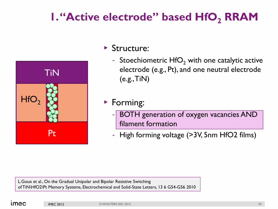
1. “Active electrode” based HfO2 RRAM
▸ Structure:
- Stoechiometric HfO2 with one catalytic active
electrode (e.g., Pt), and one neutral electrode
(e.g., TiN)
▸ Forming:
- BOTH generation of oxygen vacancies AND
filament formation
- High forming voltage (>3V, 5nm HfO2 films)
D.WOUTERS SISC 2012
TiN
Pt
L.Goux et al., On the Gradual Unipolar and Bipolar Resistive Switching
of TiN\HfO2\Pt Memory Systems, Electrochemical and Solid-State Letters, 13 6 G54-G56 2010
HfO2
74 IMEC 2012

© IMEC 2010 / CONFIDENTIAL
1. “Active electrode” based HfO2 RRAM
D.WOUTERS SISC 2012
[1] L.Goux et al., Electrochemical and Solid-State Letters, 13 6 G54-G56 2010
[2] L.Goux et alAPPLIED PHYSICS LETTERS 97, 243509 2010
▸ Reset : anodic oxidation
- Requires positive voltage at active electrode
re-oxidation of filament at Pt anode interface [1]
Oxygen supply from active electrode
▸ Set :
- Vacancy creation + thermal assisted outdiffusion
& drift of oxygen
▸ No closed system:
- Generation/recombination of oxygen vacancies
Main mechanism = transport of Oxygen
atmosphere effects [2]
▸ Main difference with unipolar operation
- Drift-assisted motion of charged oxygen species
results in improved cyclability
O2
75 IMEC 2012

© IMEC 2010 / CONFIDENTIAL
M-cap HfO2
2. “Oxygen vacancy drift” based RRAM
D.WOUTERS SISC 2012
After
processing
oxygen vacancy reservoir excess oxygen
▸ Controlled introduction of oxygen
vacancy by process
- Oxygen scavenging metal cap layer on top
of stoechiometric HfO2 (ALD)
Ti, Hf, Ta,....
Local formation of HfO2-d
- Deposition of substoichiometric HfOx
(PVD)
▸ Need for asymmetric profile of
oxygen vacancies
- Otherwise competing switching layers [1]
Stack M-
Cap HfO2
TE
BE
76 IMEC 2012
F.Nardi et al, “Complementary switching in metal oxides: toward diode-less Xbad RRAMs”, IEDM 2011

© IMEC 2010 / CONFIDENTIAL 77 2012 / imec
Evidence of O migration in Hf CAP
D.WOUTERS SISC 2012
5.5 4.8 5.0
10.7 11.0 10.1
26.7 27.8 28.3
(5nm) HfOx
(10nm) Hf
[Govoreanu et al, SSDM2011]
Amorphous Hafnia B.Govoreanu et al, IEDM 2011
IMEC 2012

© IMEC 2010 / CONFIDENTIAL
▸ Difference in TE/BE
barrier height depending
on local [VO]
▸ Difference in positive Forming voltage and negative
Breakdown voltage
D.WOUTERS SISC 2012
Internal Photoemission measurements –
L. Pantisano et al., Microel. Eng. 88(2011)
L.Goux et al, VLSI 2012
Evidence for asymmetric VO profile
78 IMEC 2012

© IMEC 2010 / CONFIDENTIAL
M-cap HfO2
2. “Oxygen vacancy drift” based RRAM
D.WOUTERS SISC 2012
After processing
oxygen vacancy reservoir excess oxygen reservoir
After forming
M-cap HfO2
oxygen vacancy reservoir excess oxygen reservoir
conducting filament
▸ Forming:
- Main effect = filament formation ONLY
(limited creation of additional VO)
- Reduced forming conditions (<2V for 5nm
HfO2 films)
- Polarity effect
79 IMEC 2012

© IMEC 2010 / CONFIDENTIAL 80 2012 / imec
2. “Oxygen vacancy drift” based RRAM
D.WOUTERS SISC 2012
▸ Reset/Set :
- Transport = drift of oxygen vacancies
- Filament constriction shrinks/expands with
drift of oxygen vacancies up/down
▸ Closed system:
- NO Generation/Recombination of VO
Above is “intuitive model”
more detailed discussion of
operation mechanisms follows later !
IMEC 2012

© IMEC 2010 / CONFIDENTIAL
Comparison
D.WOUTERS SISC 2012
Active Electrode VO Drift
Filament Oxygen Vacancies Oxygen Vacancies
Generation of VO Forming Process
Forming (5nm
HfO2)
High V (>3V) Low V (<3V), tunable
Reset Catalytic oxidation
of filament
Filament narrowing
Defect model Oxygen diffusion &
drift
Generation/
Recombination of VO
Drift of VO
System Open (loss of O) Closed (no VO G/R)
Cyclability Limited High
81 IMEC 2012
Only ”VO drift” RRAM further discussed

© IMEC 2010 / CONFIDENTIAL
>1010 Cyclability of HfO2 RRAM
D.WOUTERS SISC 2012 82
By balancing the SET pulse WL=1V, BL=1.8V, 5ns and RESET pulse WL =3V, SL=1.8V, 10ns,
1010 pulse endurance could be achieved on 40nm Hf/HfO2 1T1R devices.
Y.Y.Chen, (imec) accepted for TED 2012
IMEC 2012

© IMEC 2010 / CONFIDENTIAL
HfO2 RRAM demonstrator
D.WOUTERS SISC 2012
NTHU/ITRI ISSCC 2011 1T1R
83 IMEC 2012

© IMEC 2010 / CONFIDENTIAL
RRAM : classification & materials
▸ RRAM : general definitions & some history...
▸ Classification
▸ Filamentary switching
- Properties of filamentary switching
- Thermo-chemical RRAM
- Bipolar “oxygen vacancy drift” RRAM
- Electro-chemical CBRAM
▸ Interfacial switching
D.WOUTERS SISC 2012 84 IMEC 2012

© IMEC 2010 / CONFIDENTIAL
Conductive Bridge RRAM :
“Programmable Metallization Cell”
D.WOUTERS SISC 2012 85
1D Filamentary
Material :
Ag or Cu based
Electro- chemical
Cation Source (Ag+, Cu+ or...)
Cu+
Ag+
BE
ME
TA
LIC
FIL
AM
EN
T
BIPOLAR
Ag/Cu electrode
Inert electrode
IMEC 2012

© IMEC 2010 / CONFIDENTIAL
Electrochemical filament formation
▸ Oxidation at anode: forming of metal ions (Ag Ag+ + e-)
▸ Drift of metal ions through insulating switching layer
▸ Reduction at cathode: plating out of metal ions (Ag+ + e- Ag)
- Growing filament forms “virtual cathode”
D.WOUTERS SISC 2012 86
U. Russo et al., IEEE TRANSACTIONS ON ELECTRON DEVICES, 56(5), p. 1040, 2009
Rainer Waser et al., Adv. Mater.
2009, 21, 2632–2663
IMEC 2012

© IMEC 2010 / CONFIDENTIAL
Bipolar Switching
D.WOUTERS SISC 2012 87
1.E-12
1.E-08
1.E-04
-3 -1.5 0 1.5 3
after 103 cycles
Vbit-line (V)
Curr
ent
(A)
Asymmetric switching
VRESET < VSET
Deep RESET
~ complete filament annihilation?
L.Goux et al., VLSI Technology 2012
IMEC 2012

© IMEC 2010 / CONFIDENTIAL
Materials and Structures
D.WOUTERS SISC 2012 88
Ag electrode
Inert electrode
GexSe
matrix
Ag2Se
nanoparticles
1st generation : Ag-doped chalcogenide
All-in-one, non-homogeneous material
[1] M.Kozicki,
IEEE Trans. On
Nanotechnology
4(3), 331 (2005)
Cu(X) electrode
Inert electrode
Metal-oxide
matrix
2nd generation: Metal-Oxide
Cu source separated from switching layer
K.Aratani et al., IEDM 2007
IMEC 2012

© IMEC 2010 / CONFIDENTIAL
PRO/COM OF CBRAM
D.WOUTERS SISC 2012 89
K.Aratani et al., IEDM 2007
M.Kund et al., IEDM 2005
▸ Combines high resistance window with low current operation
▸ Good cyclability (>108 cycles)
▸ Limited thermal stability of material and control of Cu diffusion
▸ Process T and High-T retention issue
▸ Low RESET voltage (disturb)
IMEC 2012

© IMEC 2010 / CONFIDENTIAL
SONY ISSCC 2011 CBRAM 1T1R
D.WOUTERS SISC 2012 90 IMEC 2012

© IMEC 2010 / CONFIDENTIAL
RRAM : classification & materials
▸ RRAM : general definitions & some history...
▸ Classification
▸ Filamentary switching
- Properties of filamentary switching
- Thermo-chemical RRAM
- Bipolar “oxygen vacancy drift” RRAM
- Electro-chemical CBRAM
▸ Interfacial switching
D.WOUTERS SISC 2012 91 IMEC 2012

© IMEC 2010 / CONFIDENTIAL
2D switching RRAM
D.WOUTERS SISC 2012 92
Schottky barrier
2D
Interfacial
TE
BE
exchange layer
O vacancy,...
perovskite
BIPOLAR
Akihito Sawa, MaterialsToday 11(6) p.28 2008
Material :
complex oxides
(doped perovskites)
noble (Pt) electrode
IMEC 2012

© IMEC 2010 / CONFIDENTIAL
Mechanism: modulation of Schottky
barrier
D.WOUTERS SISC 2012 93
Akihito Sawa, MaterialsToday 11(6) p.28 2008 by moving oxygen vacancies
to or from the interface
IMEC 2012

© IMEC 2010 / CONFIDENTIAL
Area scaling as fingerprint of 2D switch
D.WOUTERS SISC 2012 94
H.Sim et al., IEDM 2005
IMEC 2012

© IMEC 2010 / CONFIDENTIAL
PRO/CON 2D Interfacial Switching
▸ Materials :
- Complex perovskite oxides : process (in) compatibility ?
- Pt electrode required for good Schottky barriers
▸ Thick films :
- may compromise scaling
▸ Asymmetry and Non-linearity of LRS I-V behavior:
- Suitable for Self Rectifying Cell
“
D.WOUTERS SISC 2012 95 IMEC 2012

© IMEC 2010 / CONFIDENTIAL
Interfacial switching key for Self
Rectifying Cell...
D.WOUTERS SISC 2012 96
J.Sanchez, NCCAVS Thin Film User Group Meeting, 10/14/09
Current limited by QM tunneling through
tunneling layer
Barrier height influenced by oxygen
vacancies driven in our out the TO
IMEC 2012

© IMEC 2010 / CONFIDENTIAL
UNITY SC ISSCC2010 SRC
D.WOUTERS SISC 2012 97 IMEC 2012
IMEC 2012

© IMEC 2010 / CONFIDENTIAL
Outline
D.WOUTERS SISC 2012 98
RRAM : Classification
Need for new Non Volatile Memory?
RRAM : Memory Structure
RRAM: Status
Materials
Device
IMEC 2012
Resistive Switching Behavior

© IMEC 2010 / CONFIDENTIAL
RRAM Memory Structure
▸ Memory Cell > RRAM element
▸ Different RRAM Cell configurations
▸ 3D RRAM architectures
D.WOUTERS SISC 2012 99 IMEC 2012

© IMEC 2010 / CONFIDENTIAL
RRAM Cell and Array configurations
▸ RRAM element = RRAM cell ?
- Raw Cross Point array = highest density configuration
- Cell size = 4F2
D.WOUTERS SISC 2012
Akihito Sawa,
MaterialsTodayJUNE 2008 |
VOLUME 11 | NUMBER 6 p. 28
100 IMEC 2012

© IMEC 2010 / CONFIDENTIAL
RAW XP LIMITATIONS
▸ Read errors due to sneak current paths
▸ Program disturbs on half-select cells (1/2 or 1/3 V
scheme)
▸ Power dissipation due to current through half-
selected cells
D.WOUTERS SISC 2012 101
E.Linn en al, NATURE MATERIALS VOL 9 p. 403 MAY 2010 J.Liang et al., IEEE TRANSACTIONS ON ELECTRON
DEVICES, VOL. 57, NO. 10, p.2532 OCTOBER 2010
IMEC 2012

© IMEC 2010 / CONFIDENTIAL
RAW XP ARRAY EXPLORATION
D.WOUTERS SISC 2012 102
J.Liang et al., IEEE TRANSACTIONS ON ELECTRON
DEVICES, VOL. 57, NO. 10, p.2532 OCTOBER 2010
Very limited array sizes, dependent on
Ron/Roff ratio, Ron value, non-linearity, etc.
Solution ? Need for selector element in RRAM cell
An Chen, Nanotechnology (IEEE-NANO), pp.1767-1771, 15-18 Aug. 2011
IMEC 2012

© IMEC 2010 / CONFIDENTIAL
1T1R cell
Transistor is ideal selector
▸ Both isolation switch and current limiter (during SET)
▸ 3-terminal device : large cell
▸ Best suited for embedded RRAM
D.WOUTERS SISC 2012 103
0 1 2 3 40
200
400Reset
Set
I(mA
)V_topelectrode_NiOcell (V)
Forming
F.Nardi et al, IMW 2010
F,Chen ITRI
IMEC 2012
© IMEC 2010 / CONFIDENTIAL
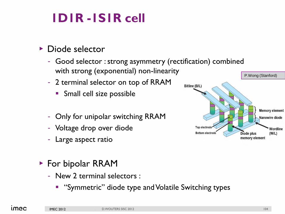
1D1R -1S1R cell
▸ Diode selector
- Good selector : strong asymmetry (rectification) combined
with strong (exponential) non-linearity
- 2 terminal selector on top of RRAM
Small cell size possible
- Only for unipolar switching RRAM
- Voltage drop over diode
- Large aspect ratio
▸ For bipolar RRAM
- New 2 terminal selectors :
“Symmetric” diode type and Volatile Switching types
D.WOUTERS SISC 2012 104
P.Wong (Stanford)
IMEC 2012

© IMEC 2010 / CONFIDENTIAL
2- Terminal SELECTOR concepts
D.WOUTERS SISC 2012
unipolar bipolar
Diode types
-p(i)n diode
-Schottky diode
Symmetric diode type
-Zener
-Punch Through Diode
Volatile switching
type
-MOTT
-OTS
-MIEC
VO2
Chalcogenide novel
materials
Diode types
MOx pn/Schottky diode
Using
semiconducting
material
Y.Sasago et al, VLSI Tech.Symp. 2009
M-J. Lee, Advanced Functional Materials,
2008, 18, p.1
M-J. Lee, Advanced Materials, 2007, 19, p.3919
D.Kau et al, IEDM 2009
Ion Conductor
K.Gopalankhrisnan et al. VLSI 2010
Symmetric diode
type
- Schottky Diode
-Tunnel
Diode
MOx
J-J. Huang, EDL 11(10) 2011
J-J. Huang, IEDM 2011
105 IMEC 2012

© IMEC 2012 / CONFIDENTIAL
3D Stackable RRAM 3D VRRAM
D.WOUTERS SISC 2012
3D RRAM ARRAY OPTIONS
106 IMEC 2012

© IMEC 2012 / CONFIDENTIAL
3D Stackable RRAM
D.WOUTERS SISC 2012
3D RRAM ARRAY OPTIONS
107 IMEC 2012
M. Lee, et al., IEDM Tech. Dig. 2007
“pseudo 3D” = 2D stacking
3D Matrix, Semiconductor International , 7 Jan. 2005 1S1R

© IMEC 2012 / CONFIDENTIAL
3D Stackable RRAM 3D VRRAM
D.WOUTERS SISC 2012
3D RRAM ARRAY OPTIONS
108 IMEC 2012
H.Yoon, et al., VLSI Tech. 2009
“true” 3D
No place for
selector !
SRC

© IMEC 2010 / CONFIDENTIAL
Self Rectifying Cell
▸ Cell with strong nonlinearity (in ON state)
▸ Some proposals, but still limited nonlinearity
D.WOUTERS SISC 2012 109
Hynix VLSI Tech. 2012 M.Jo et al, VLSI Tech. 2010
Pt/
Al/PC
MO
/Pt
IMEC 2012

© IMEC 2010 / CONFIDENTIAL 110 © IMEC 2012 / CONFIDENTIAL
BIT CELL SELECTION
D.WOUTERS SISC 2012
Embedded 2D stackable array 3D vertical RRAM
PROS Easy to optimize
high ON/OFF ratio
Easy to integrate in
CMOS BEOL (3 extra
masks vs 8 for Flash)
4F2 4F2
thin
CONS Big cell,
not stackable
Stackable? No real solution yet
IMEC 2012

© IMEC 2010 / CONFIDENTIAL
Outline
D.WOUTERS SISC 2012 111
RRAM : Classification
Need for new Non Volatile Memory?
RRAM : Memory Structure
RRAM: Status
Materials
Device
IMEC 2012
Resistive Switching Behavior

© IMEC 2010 / CONFIDENTIAL
RRAM switching behavior
Detailed understanding of RRAM device
behavior required for :
▸ Tuning memory operation conditions
▸ Predicting reliability
▸ Optimizing material stack
Not just process, but detailed kinetics of device
behavior
Focus on oxygen-drift HfO2 RRAM
▸ More generally applicable to bipolar filamentary
switching (Ox)RRAM D.WOUTERS SISC 2012 112 IMEC 2012 IMEC 2012

© IMEC 2010 / CONFIDENTIAL
Understanding RRAM switching
1. Modeling approaches
2. Intrinsic RRAM switching
3. QPC filament conduction model
4. Hourglass switching model
D.WOUTERS SISC 2012 113 IMEC 2012

© IMEC 2010 / CONFIDENTIAL
Modeling approaches
How to understand filamentary switching ?
(i) use your imagination
D.WOUTERS SISC 2012 114 IMEC 2012

© IMEC 2010 / CONFIDENTIAL
The Artist approach to RRAM
D.WOUTERS SISC 2012 115 IMEC 2012

© IMEC 2010 / CONFIDENTIAL IMEC 2012
(too) many RRAM artist styles ?
D.WOUTERS SISC 2012 116
N.Xu et al, VLSI Tech 2008
D. IELMINI TED 2011
G.Bersuker, 2nd RRAM workshop 2012
K.Kamiya et al, APL 100 2012
L.Goux et al, ESSL 14(6) 2011 S.Larentis et al, TED 59(9) 2012

© IMEC 2010 / CONFIDENTIAL
Relevance of Science Art ?
▸ Visualize possible processes
- Generation of new insights
- May hint to possible flaws in the assumed model
- Explaining RRAM to your management
▸ Not a proof on its own but a good add-on of
theoretical models
▸ Limitations :
- Limited to classical “particle” models : problem to visualize
Quantum-Mechanical processes...
D.WOUTERS SISC 2012 117 IMEC 2012

© IMEC 2010 / CONFIDENTIAL
Modeling approaches
How to understand filamentary switching ?
(i) use your imagination : the “artist” approach
(ii) bottom up: material scientist approach
D.WOUTERS SISC 2012 118 IMEC 2012

© IMEC 2010 / CONFIDENTIAL
BOTTOM-UP approach
▸ List up all possible physical processes potentially involved in
the resistive switching...
D.WOUTERS SISC 2012 119
R.Waser, IEDM short course 2011
IMEC 2012

© IMEC 2010 / CONFIDENTIAL
BOTTOM-UP approach critique
Too many possible equations to cope with.
▸ How to select relevant/dominating processes?
▸ A lot of different processes described by similar
“exponential” math....
You only get out what you put in
▸ unexpected processes may play a role
Classical “continuum” approach
▸ Finite element modeling of current & temperature
based on local conductivity and Joule heating
▸ Cannot account for Quantum-Mechanical effects!
D.WOUTERS SISC 2012 120 IMEC 2012

© IMEC 2010 / CONFIDENTIAL IMEC 2012
Example : V-t dilemma in CBRAM
▸ Which is the rate limiting process in CBRAM?
- (i) anodic dissolution of Cu according to Cu⇒Cuz++ze−
- (ii) drift of the Cuz+cations across the SiO2
- (iii) cathodic deposition at the Pt electrode by Cuz++ze−⇒ Cu.
▸ All 3 give exponential !
▸ Argued that (iii) dominates through the charge
transfer rate at the Cu/SiO2 interface described by the
Butler–Volmer equation
D.WOUTERS SISC 2012 121
C.Schindler et al., Appl.Phys. Lett, 94, 072109, 2009

© IMEC 2010 / CONFIDENTIAL IMEC 2012
How deep at the bottom to start?
▸ The “ultimate” bottom : Ab Initio
- Obtained A.I. results have been revealing on the behavior of
oxygen defects (charge states, formation energy, diffusion
constants) and their coalescence into filaments
- But limited to study specific effects
D.WOUTERS SISC 2012 122
Katsumasa Kamiya et al, Appl. Phys.
Lett. 100, 073502 (2012);
S. Park, et al.,IEEE Electron Device Letters, 32, 197, 2011.

© IMEC 2010 / CONFIDENTIAL
Modeling approaches
How to understand filamentary switching ?
(i) use your imagination : the “artist” approach
(ii) bottom up: the material scientist approach
(iii) top-down: the EE approach
D.WOUTERS SISC 2012 123 IMEC 2012

© IMEC 2010 / CONFIDENTIAL
The EE approach
▸ Start from device behavior: electrical characterization
- Conduction in different R states
- Intrinsic versus extrinsic switching curves
- Try to analyze the important effects (AC vs DC, temperature)
- Effect of sample geometry (e.g. device area)
- Others: RTN...
▸ Come up with a model
- Filament model for conduction in HRS and LRS
- Kinetic model for switching
▸ Check if we can simulate all electrical data with
consistent and physically “sound” set of parameters
D.WOUTERS SISC 2012 124 IMEC 2012

© IMEC 2010 / CONFIDENTIAL
TOP-DOWN approach critique
▸ Behavioral model...
... but preferentially physics based
link to actual material processes
= “MEET IN THE MIDDLE”
▸ Device behavior can be influenced by
- Material
- Device structure
- Process effects
May limit a more general value..
D.WOUTERS SISC 2012 125 IMEC 2012

© IMEC 2010 / CONFIDENTIAL
Understanding RRAM switching
1. Modeling approaches
2. Intrinsic RRAM switching
3. QPC filament conduction model
4. Hourglass switching model
D.WOUTERS SISC 2012 126 IMEC 2012

© IMEC 2010 / CONFIDENTIAL
DC switching measurements : 0T1R
Current compliance hides (SET) switching
D.WOUTERS SISC 2012 127
Measured I-V (= extrinsic)
(A)
VC
IC
VSET
(V)
Easy to measureand always known
Compliance limited(A)
VC
IC
(V)
VSET
?
Which is exact(V,I) trajectory ?
I-V of TMO ( = intrinsic)
(only 2 points known)
F.Nardi et al, Trans.El.Dev. 59(9), p.2461, 2012
HfO2 RRAM cell
IMEC 2012

© IMEC 2010 / CONFIDENTIAL
DC switching measurements : 1T1R
▸ Total cell voltage during SET switching known
▸ But high non-linearity of Transistor current
IDS=f(VG,VDS) prohibit calculation of voltage over
RRAM
D.WOUTERS SISC 2012 128
D.Ielmini , Trans.El.Dev. 58(12), p.4310 (2011)
IMEC 2012

© IMEC 2010 / CONFIDENTIAL
DC switching measurements : 2R
Using a linear integrated component (resistor):
▸ we can limit current
▸ We can recover the SET trajectory:
VRRAM = Vapplied-I.RA
D.WOUTERS SISC 2012 129
SL
BL
TE
BEVR
RA
MV
RA
+
-
VA
RA2R
WT
LTETE BE cell
RA
2R test structures:
0.05 0.10 0.15
50
100
150
200
250
300
350 TE Line 25C
TE Line 125C
Lin
e s
quare
resis
tance R
S [
]
TiN line CD [um]4 P
oin
t
5um
len
target
Calibration of sqr res:
NOTE: nominal CD and effective resistances
Imec crossbar RRAM
A. Fantini et al, IMW 2012
IMEC 2012

© IMEC 2010 / CONFIDENTIAL
Extrinsic Switching in 2R
D.WOUTERS SISC 2012 130
-1.5 -1.0 -0.5 0.0 0.5 1.00
25µ
50µ
75µ
100µ
125µ
Voltage (V)
|Curr
ent| (
A)
SETRES
VT,SET
2
1
3
4
-5.6k
Abrupt
RESETGradual
Increase
Measured I-V (Extrinsic)
Applied Voltage VA (V)
IRES <= ISET
• RESET is very abrupt. In clear contrast to “analog” reset.
• Gradual (linear) SET after first “jump”
• SET Linearly returns to origin with a different (lower) slope
• Onset of RESET symmetrically occurs at the same end point of SET sweep.
A. Fantini et al, IMW 2012
IMEC 2012

© IMEC 2010 / CONFIDENTIAL
Extrinsic Intrinsic switching in 2R
D.WOUTERS SISC 2012 131
-1.5 -1.0 -0.5 0.0 0.5 1.00
25µ
50µ
75µ
100µ
125µ
| Voltage | (V)
|Curr
ent| (
A)
SETRES
1
23
4Vtrig
Vtran
s
|Vtran
s|“EXT”
“EXT”
“INT”2
1
3
4
C
A
B
D
Voltage (V)
Current increases
at constant V
A. SET triggering followed by rapid “snapback”: with slope (-1/RA)
B. “Filament” then grows (i.e. current increases) at constant voltage
(“transition voltage”) Vtrans
C. RESET transition triggers at symmetrical (-Vtrans) voltage with fast voltage
increase (“snapforward”) with slope (-1/RA)
D. “Filament” then shrinks at approx constant saturation current IR,sat
A. Fantini et al, IMW 2012
IMEC 2012

© IMEC 2010 / CONFIDENTIAL 132 2012 / imec
Voltage controlled switching :
definition of Transition Voltage
D.WOUTERS SISC 2012
VT,SET V
|I|
VTRANS -VTRANS
-VRESET_MAX
Filament grows at constant
voltage = VTRANS
At symmetric voltage,
filament starts to RESET
VTRANS is the minimum voltage required for switching
IMEC 2012

© IMEC 2010 / CONFIDENTIAL
Fingerprint of filamentary switching?
▸ Analysis of different RRAM material systems show
similar intrinsic switching characteristics
D.WOUTERS SISC 2012 133
VTRANS ~0.2V
SET RESET
TABLE I
PARAMETERS FOR DIFFERENT ANALYZED CRS CELLS
RRAM element Imax RLRSa RSERIES VTRANS
b Ref
TiN\HfO2\Hf\TiN 3 mA ~140 180 ~0.36 V -
Pt\SiO2\GeSe\Cu 0.9 mA ~264 1050 ~0.18 V [1]
Pt\SiO2\Cu 15 mA ~27 220 ~0.26 V [2]
Pt\Ta2O5-x\TaO2-x\Pt 40 mA ~10 k 44 k ~0.40 V [4]
Au\CNT\a-C\Au 80 mA ~24 k 70 k ~1.85 V [5] aAverage for Top and Bottom RE; bAverage of + and - VTRANS
D.Wouters, EDL 33(8), p. 1186 (2012)
Pt\SiO2\GeSe\Cu
CBRAM cell
▸ Transition Voltage = material
dependent parameter?
IMEC 2012

© IMEC 2010 / CONFIDENTIAL
Current scaling in 2R
D.WOUTERS SISC 2012 134
0
50µ
100µ
150µ
200µ
250µ
Cu
rre
nt
(A)
0.0 0.5 1.0 1.50
50µ
100µ
150µ
200µ
250µ
Ab
s C
urr
en
t (A
)
|VRRAM
| (V)
0
10µ
20µ
30µ
40µ
50µ
60µ
0.0 0.5 1.0 1.50
10µ
20µ
30µ
40µ
50µ
60µ
|VRRAM
| (V)
0
4µ
8µ
12µ
0.0 0.5 1.0 1.50
4µ
8µ
12µ
|VRRAM
| (V)
RA (0.25∙G0)-1RA (0.93 ∙ G0)
-1RA (4.1∙G0)-1
Vtr
ans
Vtr
ans
Vtr
ans
SET
RES
-3.1k -55k-14k
(a) (b) (c)
Important observations (mean values):
• Transition voltage not depending on current level • Evidence of deviation from ohmic behavior for LRS in the lowest current
range
Non-linear I-V in the LRS
IR,SAT
IMEC 2012

© IMEC 2010 / CONFIDENTIAL
AC characterization
D.WOUTERS SISC 2012 135
▸ Typically done using voltage pulses
- Pulse effect measured by probing R after applying pulse
- No information of what happens during the pulse
D.Ielmini , IEDM 2011
IMEC 2012

© IMEC 2010 / CONFIDENTIAL
AC characterization in 2R
D.WOUTERS SISC 2012 136
▸ Transition voltage is log. depending in ramp rate
0
50µ
100µ
150µ
200µ
250µ
DC (0.5 V/s)
100 V/s
1 kV/s
10 kV/s
100 kV/s
1 MV/s
Cu
rre
nt I (A
)
0.0 0.2 0.4 0.6 0.8 1.0 1.2 1.4 1.60
50µ
100µ
150µ
200µ
250µ
| C
urr
en
t | (A
)
|VRRAM
| (V)
0
5µ
10µ
15µ
20µ
25µ
30µ
DC (0.5 V/s)
100 V/s
1 kV/s
10 kV/s
100 kV/s
1 MV/s
Cu
rre
nt I (A
)
0.0 0.2 0.4 0.6 0.8 1.0 1.2 1.4 1.60
5µ
10µ
15µ
20µ
25µ
30µ
| C
urr
en
t | (A
)
|VRRAM
| (V)
-3.1k
25 C, SETIncreasing
r = dVA/dt
25 C, RES
25 C, SET
-27.6k
(a) (b) (c)
0.45
0.50
0.55
0.60
0.65
0.70
0.75
Vtr
an
s (
V)
Vtrans
, 25C, RA 3.1 k
100m 1 10 100 1k 10k 100k 1M60µ
80µ
100µ
120µ
140µ
160µ
IR,sat
, 25C, RA 3.1 k
Re
se
t sa
t (A
)
Ramp rate r (V/s)
Measured @
90% Sweep V
Measured @
90% Sweep V
0
5µ
10µ
15µ
20µ
25µ
30µ
DC (0.5 V/s)
100 V/s
1 kV/s
10 kV/s
100 kV/s
1 MV/s
Cu
rre
nt I
(A)
0.0 0.2 0.4 0.6 0.8 1.0 1.2 1.4 1.6
0
5µ
10µ
15µ
20µ
25µ
30µ
| C
urr
en
t | (A
)
|VRRAM
| (V)
0
50µ
100µ
150µ
200µ
250µ
DC (0.5 V/s)
100 V/s
1 kV/s
10 kV/s
100 kV/s
1 MV/s
Cu
rre
nt I
(A)
0.0 0.2 0.4 0.6 0.8 1.0 1.2 1.4 1.6
0
50µ
100µ
150µ
200µ
250µ
| C
urr
en
t | (A
)
|VRRAM
| (V)
-3.1k
25 C, SETIncreasing
r = dVA/dt
25 C, RES
25 C, SET
25 C, RES
-27.6k
0.45
0.50
0.55
0.60
0.65
0.70
0.75
Vtr
an (
V)
Vtrans
, 25C
Vtrans
, 250C
100m 1 10 100 1k 10k 100k 1M
60µ
80µ
100µ
120µ
140µ
160µ
Reset sat (A
)
Ramp rate r (V/s)
(a) (b) (c)
~log(r)
~log(r)
A. Fantini , IMW 2012
~200 m
V
IMEC 2012

© IMEC 2010 / CONFIDENTIAL
Understanding RRAM switching
1. Modeling approaches
2. Intrinsic RRAM switching
3. QPC filament conduction model
4. Hourglass switching model
D.WOUTERS SISC 2012 137 IMEC 2012

© IMEC 2010 / CONFIDENTIAL
Non-linear & Quantized conduction
D.WOUTERS SISC 2012 138
160x10-6
120
80
40
co
nd
ucta
nce
(A
/V)
0.80.60.40.20.0Voltage Vox (V)300x10
-6
200
100
0
Co
nd
ucta
nce
ch
an
ge
(A
/V2)
0.80.60.40.20.0
Voltage Vox (V)
Co
nd
ucta
nce
Change (
A/V
2)
~0.23 V
Top electrode Voltage (V)
Half-integer values of
2e2/h = 77.5mA/V
(1/2).(2e2/h)
(2/2).(2e2/h)
(3/2).(2e2/h)
(4/2).(2e2/h)
wy
wx
10-7
10-6
10-5
10-4
Curr
en
t (A
)
0.60.40.20.0Voltage (V)
reset
2
4
1014
2
4
1015
om
eg
a p
ara
me
ter
(Hz)
10-6
2 4 6 8
10-5
2
Current @ 0.2V (A)
(d)
Room-T measurements
R.Degraeve et al, VLSI-TSA 2012
R.Degraeve et al, VLSI 2011 IMEC 2012

© IMEC 2010 / CONFIDENTIAL
Quantum Point Contact model
D.WOUTERS SISC 2012 139
R.Degraeve et al, IEDM 2010
• Inside filament : interacting
defects (oxygen vacancies)
create conductive band
• Geometric confinement
of current flow causes
bottleneck with discrete
levels
• Quantum point contact
(QPC) model for conduction
2222
02
1
2
1, ymxmeVyxE yx ww
IMEC 2012

© IMEC 2010 / CONFIDENTIAL
Fitting I-V with QPC
▸ Only wy parameter changes indicating RESET
occurs by local filament NARROWING
D.WOUTERS SISC 2012 140
wy
wx
10-7
10-6
10-5
10-4
Curr
en
t (A
)
0.60.40.20.0Voltage (V)
reset
2
4
1014
2
4
1015
om
eg
a p
ara
me
ter
(Hz)
10-6
2 4 6 8
10-5
2
Current @ 0.2V (A)
(d)
wy
wx
10-7
10-6
10-5
10-4
Curr
en
t (A
)
0.60.40.20.0Voltage (V)
reset
2
4
1014
2
4
1015
om
eg
a p
ara
me
ter
(Hz)
10-6
2 4 6 8
10-5
2
Current @ 0.2V (A)
(d)
R.Degraeve et al, VLSI 2011
IMEC 2012

© IMEC 2010 / CONFIDENTIAL
Constriction size ~ # defects
D.WOUTERS SISC 2012 141
Constriction
Ac
hc nC defects
rc
Geometric representation:
~ wx-1
~ wy-1
IMEC 2012

© IMEC 2010 / CONFIDENTIAL
Filament Model
D.WOUTERS SISC 2012 142
(II)
RESET
(III)
“deep” RESET
(I)
SET
Classical R Tunneling QPC
Not observed in our HfO2 RRAM
IMEC 2012

© IMEC 2010 / CONFIDENTIAL
Abstract filament model = Hourglass
D.WOUTERS SISC 2012 143
Hf top electrode
Top Reservoir TR
Bottom
Reservoir BR
Constriction C
TiN bottom
electrode
▸ Filament = 2 reservoirs of oxygen vacancies
connected by a constriction
▸ Size of defect reservoirs, number of defect particles,
and constriction length are fixed by Forming
R.Degraeve et al, VLSI 2012
IMEC 2012
© IMEC 2010 / CONFIDENTIAL
Understanding RRAM switching
1. Modeling approaches
2. Intrinsic RRAM switching
3. QPC filament conduction model
4. Hourglass switching model
D.WOUTERS SISC 2012 144 IMEC 2012

© IMEC 2010 / CONFIDENTIAL
Dynamic Hourglass switching model
▸ Filament = charged defects (oxygen vacancies)
- Moveable under influence of electric field
▸ Hourglass shape determined by Forming
- Hourglass ~ substoichiometric HfOx with higher oxygen
vacancy mobility :
- defects remain in hourglass
- No generation/recombination
▸ Defects can move down/up top to bottom reservoir
depending on voltage polarity
D.WOUTERS SISC 2012 145 IMEC 2012

© IMEC 2010 / CONFIDENTIAL
Dynamic Hourglass switching model
▸ 4 different defect particle fluxes at TE/BE reservoir –
constriction interfaces
- Temp. activated over voltage modified energy barrier Ea
- Depending on filling level of the reservoir
D.WOUTERS SISC 2012 146
R.Degraeve et al, VLSI 2012

© IMEC 2010 / CONFIDENTIAL
Explanation of transition voltage
▸ From this model, it is possible to calculate the
minimum voltage to move a defect in or out the
constriction in a certain amount of time
▸ This voltage ~ cte at larger currents
= “transition voltage”
▸ Independent of polarity : same voltage to start RESET
D.WOUTERS SISC 2012 147
40x10-6
30
20
10
0
Curr
ent
(A)
1.00.80.60.40.20.0
VRRAM (V)
nC=1
nC=2
nC=6
nC=15
nC=32
nC=62
nC=100
nC=150
Transition line
-26k Vtri
g
R.Degraeve et al, VLSI 2012 IMEC 2012

© IMEC 2010 / CONFIDENTIAL
Further work
Here focused on SET behavior and explanation of
“constant voltage” filament growth
Hourglass model can explain also other effects, as:
▸ “overcurrent” in 1st RESET after forming
▸ RESET behavior as function of V and time’
▸ Fluctuationns and Disturb of RESETstate
▸ ....
D.WOUTERS SISC 2012 148 IMEC 2012

© IMEC 2010 / CONFIDENTIAL
Outline
D.WOUTERS SISC 2012 149
RRAM : Classification
Need for new Non Volatile Memory?
RRAM : Memory Structure
RRAM: Status
Materials
Device
IMEC 2012
Resistive Switching Behavior

© IMEC 2010 / CONFIDENTIAL
RRAM Status
▸ Performance and Endurance
▸ Scalability
▸ Demonstrators
▸ Product announcements
D.WOUTERS SISC 2012 150 IMEC 2012

© IMEC 2010 / CONFIDENTIAL D.WOUTERS SISC 2012 151 IMEC 2012
Steady improvement of RRAM
operation speed & current
Slide courtesy G.Jurczak, imec

© IMEC 2010 / CONFIDENTIAL
> 1012 “unlimited” cyclability in TaOx
D.WOUTERS SISC 2012 152
Y-B.Kim et al, VLSI Technology 2011
IMEC 2012

© IMEC 2010 / CONFIDENTIAL
<10nm scalability of HfO2 RRAM cells
D.WOUTERS SISC 2012 153
B.Govoreanu et al IEDM 2011
G.Kar et al VLSI 2012
IMEC 2012

© IMEC 2010 / CONFIDENTIAL
ARRAY DEMONSTRATIONS OF 1T-1R RRAM
154
Pt/TaOx/Pt
8kb bipolar array
Panasonic, IEDM 2008
Ru/TiOx/TaOx/Ru
1kb unipolar array
NEC, VLSI 2010
TaN/CuSixOy/Cu
1Mb bipolar array
SMIC, VLSI 2010
D.WOUTERS SISC 2012 IMEC 2012

© IMEC 2010 / CONFIDENTIAL
ARRAY DEMONSTRATIONS OF 1S-1R RRAM
D.WOUTERS SISC 2012
Panasonic, ISSCC 2012 8Mb,
Unity, ISSCC 2010 64Mb, 130nm
HYNIX, VLSI 2012 54nm CMOS platform
155 IMEC 2012
© IMEC 2010 / CONFIDENTIAL
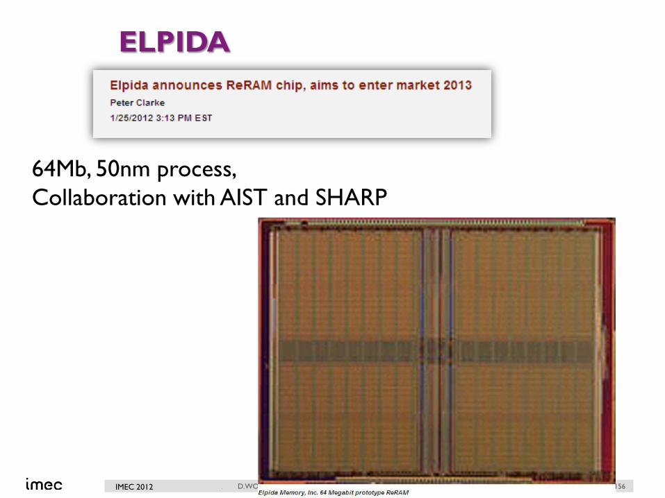
ELPIDA
D.WOUTERS SISC 2012
64Mb, 50nm process,
Collaboration with AIST and SHARP
156 IMEC 2012

© IMEC 2010 / CONFIDENTIAL
Toshiba_Sandisk will announce a 32Gb
1D1R RRAM in 24nm @ ISSCC2013
D.WOUTERS SISC 2012 157
EETimes Asia 21 Nov. 2012
RRAM is fastly emerging !
IMEC 2012

© IMEC 2010 / CONFIDENTIAL
Conclusions
▸ Short introduction in why and how of RRAM
▸ Exciting material and device research field
- a lot of understanding during last years
▸ RRAM emerging to reality ?
D.WOUTERS SISC 2012 158
© IMEC 2010 / CONFIDENTIAL
Acknowledgements:
• Many contributions from the imec RRAM team, especially:
Y.Y,Chen, S.Clima, R.Degraeve, L.Goux, B.Govereanu, G.S.Kar, A.Fantini,
L.Zhang
• Program director : M.Jurczak
• Industrial partners in imec’s Core CMOS program
Thank You !
43rd IEEE Semiconductor
Interface Specialists
Conference

© IMEC 2010 / CONFIDENTIAL

© IMEC 2010 / CONFIDENTIAL 161 2012 / imec
type PCRAM OxRRAM STT-RAM
Operation Write Speed >10nsec ~5nsec ~1nsec
Write current ~10’s of uA ~uA’s 1-10MA/cm2
MLC? Yes ? No
Endurance 109 1012 1015 (infinite?)
Ron/Roff >103 10-100 ~2
CMOS
compatibility
Switching
Voltage
2 -4 V 2-4 V (+ needs Forming)
1-2 V
Materials GeSbTe Standard (HfO2) NS Metal stacks
Process
limitations
None? (non-
standard material)
None
Limited thermal
stability
Scalability Limitations Current (need sub-litho
scaling)
Variability (localized thin
filament)
Retention (~Volume)
Configuration Selector 1D1R 1T1R-1S1R 1T1R
2D stackable ? Yes No
Target
applications ?
(NOR-Flash)
SCM?
Embedded ?
SCM
(NAND) Flash
Embedded ?
DRAM
Embedded ?
D.WOUTERS SISC 2012