Embed Size (px)
Citation preview

Forschungszentrum Jülich
Resistive Switching inResistive Switching in Metal-Insulator-Metal Junctions
H. Kohlstedt*
Forschungszentrum Jülich GmbH,Institut für Festkörperforschung and CNI, the Center of Nanoelectronic
Systems and Information Technology GermanySystems and Information Technology, Germany
*Present address:
Center of
University of California, BerkeleyDepartment of Material Science and Engineeringand Berkeley Lab - Advanced Light Source
Center ofNanoelectronic Systems forInformation Technology
Seagate May 2006: email: [email protected]

Contents
I. IntroductionRandom Access Memories
II. Resistive Switching
III. Ferro-Resistive Switching
IV SummaryIV. Summary
V. Multiferroic Tunnel Junction

Charge and Resistance for RAMs
MRAMFlash
FeFETDRAM/SRAM
+-
Computational “1”
Binary FeRAM
MIM Junction(Resistive Switch)
“Write” “Read”BinaryLogic
FeRAM
Computational “0”Carbon nanotubes
Ovonic Molecular Memory(single molecule)
Conductive bridge(Solid State Electrolyte)
+
-

What is a resistive memory?y
Read a Resistance = Resistive Memory
Examples
Charged Based: Resistance Based:
DRAMFeRAMSRAM
MRAMFlashFeFETSRAM
.....FeFETOvonic....

Why resistive storage Elements?
DRAM Cell
Word line
Bit line1T1C cell
Word line
TransistorTransistor
DRAM it
Sense Amplifier
DRAM capacitor“1” charged Cap.“0” non charged Cap.CBL
Cmin ≅ 30 fF

Planar DRAM CapacitorPlanar DRAM Capacitor
ACmin ≅ 30 fF SiO2 thickness dA
Q = C U; C = ε0εA / dQ C U; C ε0εA / d
Decrease capacitor footprint (area A) ⇒ reduces C (Cmin limit)
Reduce dielectric thickness d tunneling limit (approx 2nm)• Reduce dielectric thickness d, tunneling limit (approx. 2nm)• Increase area by using 3-D structures (keep footprint)• Use high-k dielectrics (process compability with CMOS)

Developments: 3 D capacitors
Siemens / IBM : 1 Gbit, deep trench
metal 11 µm
bitline
Si surface
1 µm
trenchcapacitor
> 5 µmdeep
Tremendous efforts to stay on the road-mapChallenging technology – more and more expensive and complicated

FeRAM Capacitor: Pulse Polarization Switchingg
P1.0 switching
y [k
A/c
m2
P
0 0
0.5non-switching
rent
den
sity
V0 10 20 30
0.0
Cur
r
Time [ns]
Vc
Different remanent polarization states
Vbias
p
⇒ different transient current behavior to an applied voltage pulse
Integrating the current ⇒ switched charge Q and non switchedIntegrating the current ⇒ switched charge QS and non-switched charge QNS (distinction between the two logic states)
Destructive Readout

Scaling and 3D conformal Coverage
Transition from 2D to 3D technology
Minimum capacitance for sensing: 30 fFPt
2D planar
Minimum capacitance for sensing: 30 fFOperation voltage 1 VQ=CU n=Q/e3 x 10-14C needed for sensing: approx 20 000 e-3 x 10 14C needed for sensing: approx. 20.000 e
Planar capacitor:A = 100 nm x 100 nm
Ferroelectric
A 100 nm x 100 nm Pr = 10µC/cm2
10-15 CQ = P AQ P Acorresponds to 6000 e- not sufficient for data sensing!
3D h !3D approach necessary!
Conformal coverage/MOCVD mandatory
Supposed to be implemented in 2007-09for 100 nm FeRAM node technology
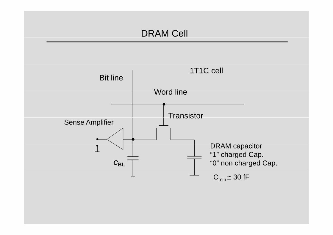
Matrix Architecture: Random Access Memory
Bit line decoder
Sense amplifierl
Data1T- 1C cell
de
co
de
r
co
ntr
olo
gic
AddressW
ord
lin
e
1T-1R cell
Renewed approach: Crossbar arrays 1-R cellRenewed approach: Crossbar arraysExtremely high scaleable

Go 3-DFirst step:
Crossbar resistor array1R ll1R cells< 10 nm feature size
3-dimensional arrayby stacking:by stacking:
Although technologicaldifficult – nothing newdifficult nothing new
Interconnects

New Nanoelectronic ArchitecturesSecond step:
G. Snider et al., Appl. Phys. A 80, 1183 (2005) – Hewlett Packard
Approach:
Activate independently at the cross pointsdifferent devices as: (switchable) resistors diodes or transistors(switchable) resistors, diodes or transistors
Create your own Computer after the fabricationprocessprocess.
Beyond conventional memory architecture!Field programmable arrays (FPGA)
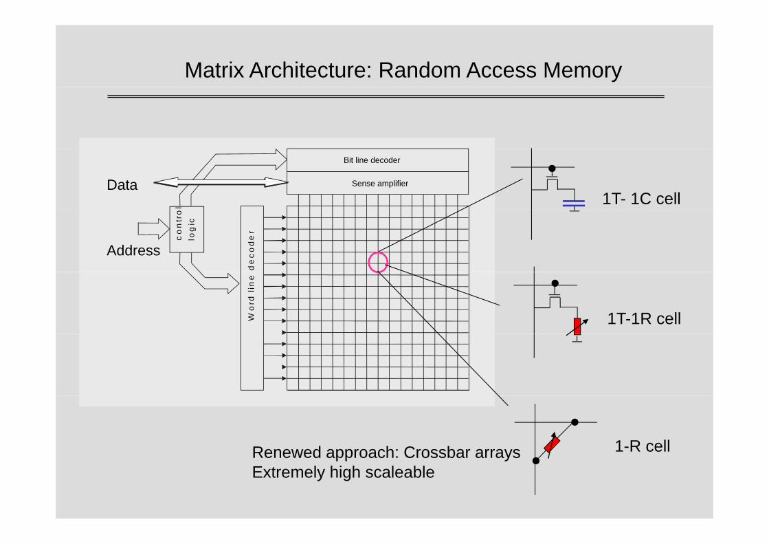
The Resistive Memory Approachy pp
Bi-stable (or multi-stable) resistors
Current“1”
Vthreshold = Vth“0”
Voltage
Vread < Vth

…more specific
Read a Resistance = Resistive Memory
S DG
M M Magnetic Tunnel Junctions
Flash
Indirect type: S D
No structural changes in theNo structural changes in thetransport region between on and off state
Direct type:
Structural changes(e.g. Phase Change)

Two Parties:
Homogenous folks:Homogenous folks:Those who believe the effectis a volume or an interface effect across the entire dielectric and/or interface
Filament (network) folks:Those who believe the effect is caused by filamanents whicheffect is caused by filamanents whichare strongly localized in an inactivesurroundingg

Overview Resistive Switches (Effects)
Homogeneous
? How homogeneous is the current transport - Filaments?
Local?Is a formation process important?
?Which role play the interfaces?
?Is the switching effect a pure electronic i i iti ?
Redox
I Red Ox + e- -
or ionic or a superposition?V Voltammogram
?Which kind of current transport is essential for R and R ??Which kind of current transport is essential for RH and RL?

Not a surprise:
Number of models > Number of groups in the field
Device Examples…

Examples: Organics
AlAlRose Bengal (70nm) or AlOx (5nm)
Rose BengalITO ZnO
B. Lüssem et al., submitted to J. Appl. Phys.
A. Bandyopadhyay and A. J. Pal, APL 82, 1215 (2003)
Even without the Polymer, the I-V curves look very similar!

Organics
D. R. Stewart et al, Nano Letters 4, 133 (2004). HP
Very different organics show very similar I_V curves!

Organics
C. N. Lau et al., Nano Lett. 4, 569 (2004).( )Hewlett-Packard
Conductive bridges (filaments) !

An Electrochemical Interface Model
C. A. Richter et al., Appl. Phys. A 80, 1355 (2005)., pp y , ( )
Oxidation and reduction of the Ti interface layer resultsin a bi-stable resistance.

Electron Trap Model: An Example
Al l t
Ma et al., Appl. Phys. Lett. 82, 1419 (2003).
Al cluster
Al-oxide barriers
Effect: Charging (decharging) by electrons in the (top) and (bottom) barriers→ Change of the conductance of the adjacent organics.
See also: Nonvolatile Memory with Multilevel Switching: A Basic Model, M. J. Rozenberg, I. H. Inoue, and M. J. SánchezPhys. Rev. Lett. 2004

Examples: Inorganics
Material: Transition metal oxide Nb2O5 (or sub-oxides)
Based on: Nb-Nb2O5-Bi
Year: 1977
D. P. Oxley, Electrocomp. Sci. and Techn. 3, 217 (1977) and references therein

Inorganics
SrRuO3/SrZrO3:Cr0.2%/AuA. Beck et al., APL 77, 139 (2000)IBM IBM ZürichIBM, IBM Zürich
SrRuO3 /SrZrO3:Cr0.2%/Pt
C. Rossel et al., J. Appl. Phys. 90, 2892 (2001). EBIC plus transport measurementIBM Zürich

Resistive switching in SrTiO3
Switching the electrical resistance ofi di id l di l ti i i l t lliindividual dislocations in single-crystallineSrTiO3K. Szot, W. Speier, G. Bihlmayer and R. WaserNature Materials 2006

Optical Inspection
K. Szot et al., Nature 2006K. Szot et al., Nature 2006
Filament formation

K. Szot et al., Nature 2006
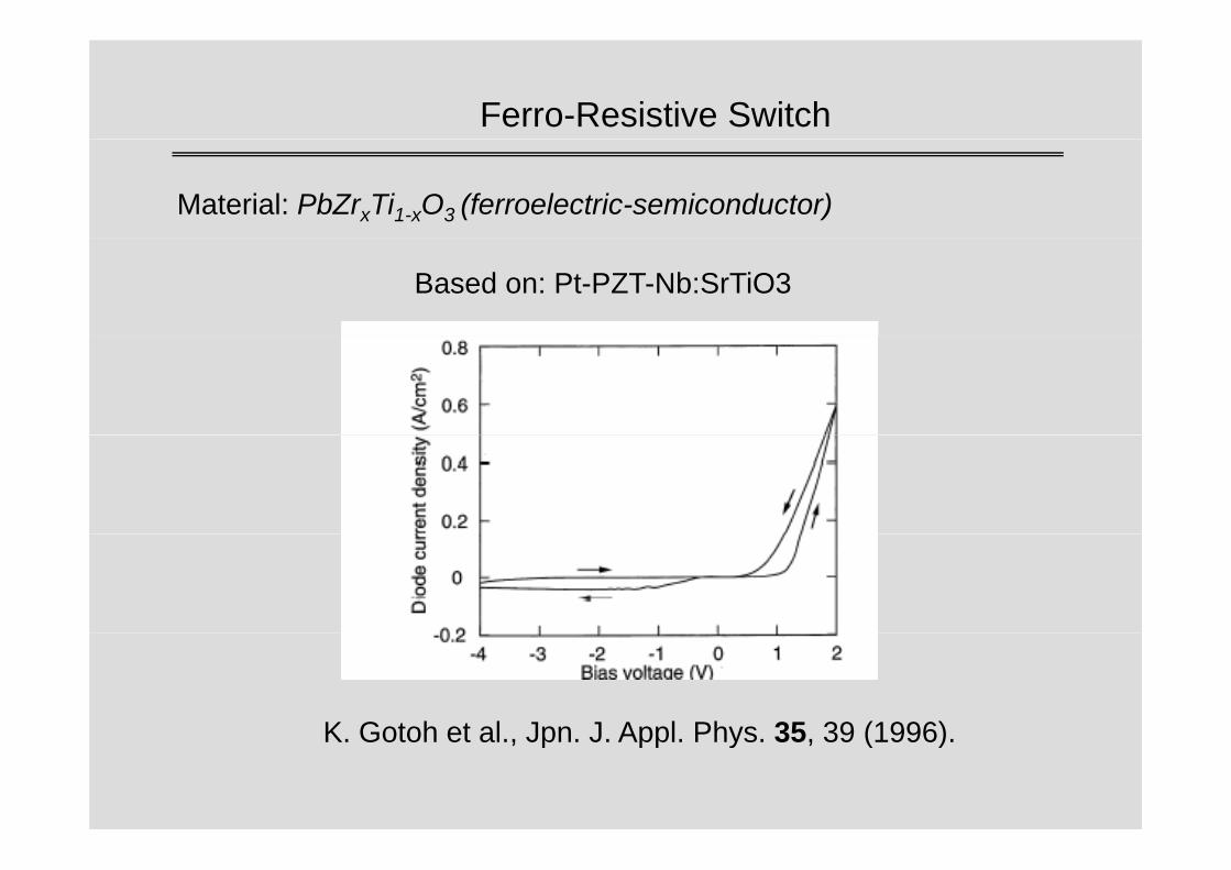
Ferro-Resistive Switch
Material: PbZrxTi1-xO3 (ferroelectric-semiconductor)
Based on: Pt-PZT-Nb:SrTiO3
K Gotoh et al Jpn J Appl Phys 35 39 (1996)K. Gotoh et al., Jpn. J. Appl. Phys. 35, 39 (1996).

Ferroresistive Switching
Self-consistent steady state solution: D ift Diff i t tDrift-Diffusion transportand the Poisson equation.
1-D Simulation of a Novel Nonvolatile Resistive Random Access Memory DeviceR. Meyer and H. Kohlstedtto be published in IEEE Transactions on Ultrasonics, Ferroelectrics and Frequency Control
K. Gotoh et al.,Jpn. J. Appl. Phys. 35, 39 (1996).

FerroResistive-RAMFerroResistive RAM
( )xρ
PSP
( )E x( )E x
( )xρ ( )e xϕ
potential barrier

FRRAMFRRAM
( )xρ
PSP
( )E x( )E x
( )xρ ( )e xϕ potential well


How to distinguish a ferroelectric origin from a non-ferroelectric one?origin from a non ferroelectric one?
4
Numerical modelExperimental result
2
3
[mA
]
-1
0
1
C
urre
nt
-2,0 -1,0 0,0 1,0 2,0
-2
-1
January, 2003
V lt [V] Voltage [V]
Although the curves look similar
R. Meyer
PZT (20/80)Pt
Thickness: 6.4 nm Although the curves look similar –its not a proof!SrRuO3
SrTiO3
Area: 3 µm2

Resistive Switching and Ferroelectric Origin (across T )(across Tc)
Switching (T < Tc) no switching (T > Tc)
BaTiO3Bulk
I IBulk
V V
but in (ultra) thin films: Tc not knownbroad phase transitionTc modified by external field Interpretation
difficult

Resistive Switching and Ferroelectric Origin
2
596597
4
TotalParasitic
Area: 0.04 μm2
595595596596
3
Parasitic
0-15 F
) CFE
0-15 F
)
593594594595
1
2
C (x
10
C FE (x
10
592592593
0
-4 -2 0 2 4U (V)

Simultaneous Measurement of different FE-Properties
A. Petraru et al., to be published in Appl. Phys. A
Laser U0 + umax sin (ωt)Detector
~ Lock-in 2
I / V Lock-in 1
PZTPt
SubstrateBase electrode
I-V converter
PZT
T d C d I ( i ti ) bi lt i lt lTo measure d33, C and I (resistive) vs. bias voltage simultaneously

Resistive Switching and Ferroelectricityd vs Bias
8x10⁻⁴
1x10⁻³
d33 vs. Bias
4x10⁻⁴
6x10⁻⁴
u.)
2x10⁻⁴
0
2x10⁻⁴
d 33 (a
.u
-6x10⁻⁴
-4x10⁻⁴
-2x10
-1.0 -0.8 -0.6 -0.4 -0.2 0.0 0.2 0.4 0.6 0.8 1.0
-8x10⁻⁴
U (V)
SrRuO3
PZT (20/80)Pt
Thickness: 30 nmArea: 3 µm23
SrTiO3
Area: 3 µm2

Resistive Switching and Ferroelectricityd C vs Bias
8x10⁻⁴
1x10⁻³
4.5
d33, C vs. Bias
4x10⁻⁴
6x10⁻⁴
3.5
4.0
u.)
)
2x10⁻⁴
0
2x10⁻⁴
2 5
3.0
d 33 (a
.u
C (p
F)
-6x10⁻⁴
-4x10⁻⁴
-2x10
2.0
2.5
-1.0 -0.8 -0.6 -0.4 -0.2 0.0 0.2 0.4 0.6 0.8 1.0
-8x10⁻⁴ 1.5
U (V)
SrRuO3
PZT (20/80)Pt
SrRuO3
SrTiO3

Resistive Switching and Ferroelectricityd C I vs Bias
8x10⁻⁴
1x10⁻³
1.0
1.24.5
d33, C, I res. vs. Bias
4x10⁻⁴
6x10⁻⁴
0.6
0.8
3.5
4.0
u.)
))
2x10⁻⁴
0
2x10⁻⁴
0.2
0.4
2 5
3.0
d 33 (a
.u
C (p
F)
I (μ
A)
-6x10⁻⁴
-4x10⁻⁴
-2x10
0 4
-0.2
0.0
2.0
2.5
-1.0 -0.8 -0.6 -0.4 -0.2 0.0 0.2 0.4 0.6 0.8 1.0
-8x10⁻⁴
-0.6
-0.4 1.5
U (V)
SrRuO3
PZT (20/80)Pt
Vc = -0.5V Vc = 0.6V
SrRuO3
SrTiO3

Increase Bias Voltage…
4
5
2
3
A)
1
0
1
I (m
A
-3
-2
-1
-1,5 -1,2 -0,9 -0,6 -0,3 0,0 0,3 0,6 0,9 1,2 1,5-4
U (V)
AFM
U (V)
Pt
PZT (20/80)
Pt
SrRuO3
SrTiO3
( )

Resistive Switching and Ferroelectricity
3x10⁻⁴
4x10⁻⁴
4
5
1x10⁻⁴
2x10⁻⁴
2
3a.
u.)
A)
-Vr
4
0
1x10
-1
0
1
d 33 (a
I (m
A
-2x10⁻⁴
-1x10⁻⁴
-3
-2
-1
-1,5 -1,2 -0,9 -0,6 -0,3 0,0 0,3 0,6 0,9 1,2 1,5-3x10⁻⁴ -4
U (V)Heat! U (V)
SrRuO3
Pt
PZT (20/80)
Pt ResistiveSwitching Vr
Heat!
Vc = -0.5V Vc = 0.6VSrRuO3
SrTiO3
Vr
Ferroelectric Switching

Resistive Switching and Ferroelectricity
Current density high enough
Pt
Current density high enough for heat generation?
SrRuO3
SrTiO3
PZT (20/80)
Estimation: I = 10 µA, rtip = 5 nmJ = I/A
J = 1.5 x 10⁷ A/cm2
If current > 10 µA,heating affects cantilever deflectionheating affects cantilever deflection

V
A
Au
5x10-46x10-4
120140
Piezorespon I
2 10-43x10-44x10-4
80100120
(a.u
.)
A)
When the current through the tip exceeds 15 µA, the piezoresponse is affected via thermal effects!
01x10-42x10 4
204060
d33
I (μ
A
I = 15 μA
-1 0 -0 5 0 0 0 5 1 0-2x10⁻⁴-1x10⁻⁴
-20020
-1,0 -0,5 0,0 0,5 1,0U (V)

Resistive Switching caused by Ferroelectricity?
Rhighnt
106
Rhigh RlowC
urre
Voltage
105
(Ωcm
)
104
ρ high
, low
(
10ρ
Pt
PZT
Pt 30 nm
10-6 1x10⁻⁵ 1x10⁻⁴
103SrRuO3
SrTiO3
PZT
Area (cm2)

Resistive Switching: Filament Model
K. Szot, FZ JülichBreakdown points
Pt Ferroelectric PbZr0.20Ti0.80O3
p(if resistive switchingappears)
30nm
SrRuO3 PtSrRuO3
SrTiO3
Schematic cross-section Top view
D. M. Schaadt et al., J. of Vacuum Science & Technology B 22, 2030 (2004)
K. Szot et al. Switching the electrical resistance of individual dislocations in single-crystalline SrTiO3, to be published in Nature Materials

Resistive Switching: Filament Model
G. DearnaleyA. M. Stoneham andD. V. MorganRep. Prog. Phys.33, 1129 (1970).
G. Dearnaley,Thin Solid Films 3, 1161 (1969).

Trends
Corssbar Arrays:Resistive switches for crossbar arraysResistive switches for crossbar arrays,Many materials show resistive switching, no theoreticalunderstanding, devices performance not yet sufficient for applications,pp ,Aim: feature size < 10 nm, if possible single moleculesFabrication: Nano-imprint/Self Assembly
3 Dimensional circuits
Field Programmable Arrays
Cognitive MemoriesCognitive Memories
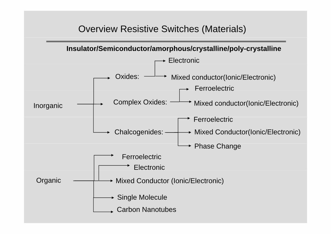
Overview Resistive Switches (Materials)
Insulator/Semiconductor/amorphous/crystalline/poly-crystallineElectronic
Oxides:
FerroelectricMixed conductor(Ionic/Electronic)
Inorganic Complex Oxides:
Ferroelectric
F l t i
Mixed conductor(Ionic/Electronic)
Chalcogenides:
Ferroelectric
Mixed Conductor(Ionic/Electronic)
Ph ChFerroelectric
Phase Change
Electronic
Organic Mixed Conductor (Ionic/Electronic)
Single MoleculeSingle Molecule
Carbon Nanotubes

Summary
C b tt ti f hi h d it i•Crossbar arrays are attractive for high-density memories•Resistive switching is observed in many different materials•Up to now no clear theoretical background•The resistive switching is often a result of conductive bridges
•Ferroresistive material show resistive switchinggThe origin of the effect can be analyzed by simultanous measurementOf different ferroelectric properties

Research Center Juelich: External Collaborations:
A Petraru (Post Doc) N A Pertsev Landau TheoryA. Petraru (Post Doc)A. Kaiser (Student)
U. Poppe, J. Schubert, C. Buchal
N. A. Pertsev – Landau Theory A. F. Ioffe Physico-Technical Institute, Russian Academy of Sciences, St. Petersburg, Russia.
D Schlom Complex Oxides MBEM. Indlekofer
R Meyer
D. Schlom – Complex Oxides MBEPenn State University, Depart. of Material Science, USA
R. Meyer
H. SchroederPh. Ghosez – Ab-initio theory on ferroelectricsUniversity of Liège, Belgium
V Nagarajan Ultra thin ferroelectric filmsC. Jia
R. Waser
V. Nagarajan- Ultra thin ferroelectric films University of South Wales, Sydney
R. RameshUniversity of Berkeley, Depart. of Material Sci., USA

AcknowledgementCenter ofNanoelectronic Systems forInformation Technologyg
Sponsors:Sponsors:
Volkswagen-Foundation:“Nano-sized ferroelectric hybrids” under contract number I/77 737.
J i t NSF DFG P j tJoint NSF-DFG Project:University of Berkeley (Material Science Department)
University of Aachen (RWTH)Research Center JülichResearch Center Jülich
„Displacive and Conductive Phenomena in Ferroelectric Thin Films:Scaling effects and switching properties“.

References:References:
Non-Volatile Memories: Overviews/Books Comment
B. Prince, Emerging Memories – TechnologyTrends, (Kluwer Academic Pub. 2002).
Explains only the rough principles:Many figures are of bad quality
Nonvolatile Semiconductor Memory Technology,IEEE Press series on microelectronic systems, ed. byW. D. Brown and J. E. Brewer 1998.
Good overview for semiconductor Flash memories
Ferroelectric Random Access Memories: H. Ishiwara,M. Okuyama, eds., Topics in Applied Physics, Vol. 93(Springer-Verlag, Berlin Heidelberg 2004).
Concentrates on ferroelectric memories
Good historical overviewJ. F. Scott, Ferroelectric Memories, Springer Series in Adv. Microelectronics, (Springer-Verlag, BerlinHeidelberg, New York 2000).
Good historical overview,Explains also principles of Ferroelectrics
Nanoelectronicsand Information Technology, R. Waser ed., Adv Electr Mat And Novel Dev
Broad Textbook with various topics in nanoelectronics,Some Chapters on Non-Volatile Memories:FRAM, FeFET, MRAM, Adv. Electr. Mat. And Novel Dev.
Wiley-VCH Verlag Weinheim 2002., e , ,
Phase Change Materials


![Resistive switching in Pt/TiO 2/Pt - COnnecting REpositories · 2016. 5. 26. · Resistive switching of transition metal oxide (TMO) materials including TiO2[1 3], NiO[4, 5], and](https://img.pdfslide.us/doc/110x75/60c06d4ba8da2d61d21f28d3/resistive-switching-in-pttio-2pt-connecting-repositories-2016-5-26-resistive.jpg)