Embed Size (px)
Citation preview
Broadcast Technology No.62, Autumn 2015 ● C NHK STRL10
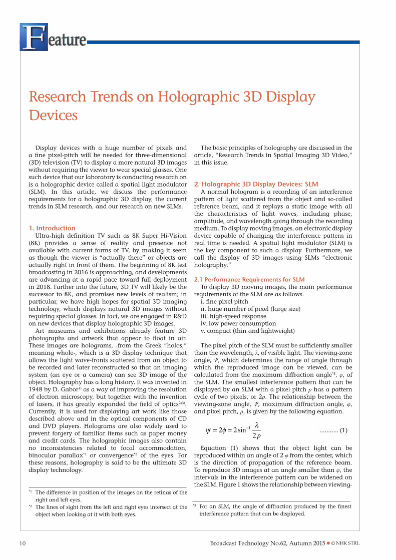
Display devices with a huge number of pixels and a fine pixel-pitch will be needed for three-dimensional (3D) television (TV) to display a more natural 3D images without requiring the viewer to wear special glasses. One such device that our laboratory is conducting research on is a holographic device called a spatial light modulator (SLM). In this article, we discuss the performance requirements for a holographic 3D display, the current trends in SLM research, and our research on new SLMs.
1. IntroductionUltra-high definition TV such as 8K Super Hi-Vision
(8K) provides a sense of reality and presence not available with current forms of TV, by making it seem as though the viewer is “actually there” or objects are actually right in front of them. The beginning of 8K test broadcasting in 2016 is approaching, and developments are advancing at a rapid pace toward full deployment in 2018. Farther into the future, 3D TV will likely be the successor to 8K, and promises new levels of realism; in particular, we have high hopes for spatial 3D imaging technology, which displays natural 3D images without requiring special glasses. In fact, we are engaged in R&D on new devices that display holographic 3D images.
Art museums and exhibitions already feature 3D photographs and artwork that appear to float in air. These images are holograms, -from the Greek “holos,” meaning whole-, which is a 3D display technique that allows the light wave-fronts scattered from an object to be recorded and later reconstructed so that an imaging system (an eye or a camera) can see 3D image of the object. Holography has a long history. It was invented in 1948 by D. Gabor1) as a way of improving the resolution of electron microscopy, but together with the invention of lasers, it has greatly expanded the field of optics2)3). Currently, it is used for displaying art work like those described above and in the optical components of CD and DVD players. Holograms are also widely used to prevent forgery of familiar items such as paper money and credit cards. The holographic images also contain no inconsistencies related to focal accommodation, binocular parallax*1 or convergence*2 of the eyes. For these reasons, holography is said to be the ultimate 3D display technology.
The basic principles of holography are discussed in the article, “Research Trends in Spatial Imaging 3D Video,” in this issue.
2. Holographic 3D Display Devices: SLMA normal hologram is a recording of an interference
pattern of light scattered from the object and so-called reference beam, and it replays a static image with all the characteristics of light waves, including phase, amplitude, and wavelength going through the recording medium. To display moving images, an electronic display device capable of changing the interference pattern in real time is needed. A spatial light modulator (SLM) is the key component to such a display. Furthermore, we call the display of 3D images using SLMs “electronic holography.”
2.1 Performance Requirements for SLMTo display 3D moving images, the main performance
requirements of the SLM are as follows.i. fine pixel pitchii. huge number of pixel (large size)iii. high-speed responseiv. low power consumptionv. compact (thin and lightweight)
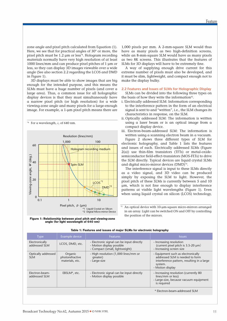
The pixel pitch of the SLM must be sufficiently smaller than the wavelength, λ, of visible light. The viewing-zone angle, Ψ, which determines the range of angle through which the reproduced image can be viewed, can be calculated from the maximum diffraction angle*3, φ, of the SLM. The smallest interference pattern that can be displayed by an SLM with a pixel pitch p has a pattern cycle of two pixels, or 2p. The relationship between the viewing-zone angle, Ψ, maximum diffraction angle, φ, and pixel pitch, p, is given by the following equation.
Equation (1) shows that the object light can be reproduced within an angle of 2 φ from the center, which is the direction of propagation of the reference beam. To reproduce 3D images at an angle smaller than φ, the intervals in the interference pattern can be widened on the SLM. Figure 1 shows the relationship between viewing-
Research Trends on Holographic 3D Display Devices
*1 The difference in position of the images on the retinas of the right and left eyes.
*2 The lines of sight from the left and right eyes intersect at the object when looking at it with both eyes.
ψ φ λ= = −
p2 2sin
21 ........... (1)
*3 For an SLM, the angle of diffraction produced by the finest interference pattern that can be displayed.
Broadcast Technology No.62, Autumn 2015 ● C NHK STRL
Feature
11
zone angle and pixel pitch calculated from Equation (1). Here, we see that for practical angles of 30° or more, the pixel pitch must be 1.2 μm or less*4. Hologram recording materials normally have very high resolution of at least 1000 lines/mm and can produce pixel pitches of 1 μm or less, so they can display 3D images viewable over a wide angle (See also section 2.2 regarding the LCOS and DMD in Figure 1).
3D displays must be able to show images that are big enough for the intended purpose, and this means the SLMs must have a huge number of pixels (and cover a large area). Thus, a common issue for all holographic display devices is that they must simultaneously have a narrow pixel pitch (or high resolution) for a wide viewing-zone angle and many pixels for a large-enough image. For example, a 1-μm pixel pitch means there are
1,000 pixels per mm. A 2-mm-square SLM would thus have as many pixels as two high-definition screens, while an 8-mm-square SLM would have as many pixels as two 8K screens. This illustrates that the features of SLMs for 3D displays will have to be extremely fine.
A way of supplying enough drive current for this extreme number of pixels must also be developed, and it must be slim, lightweight, and compact enough not to make the display bulky.
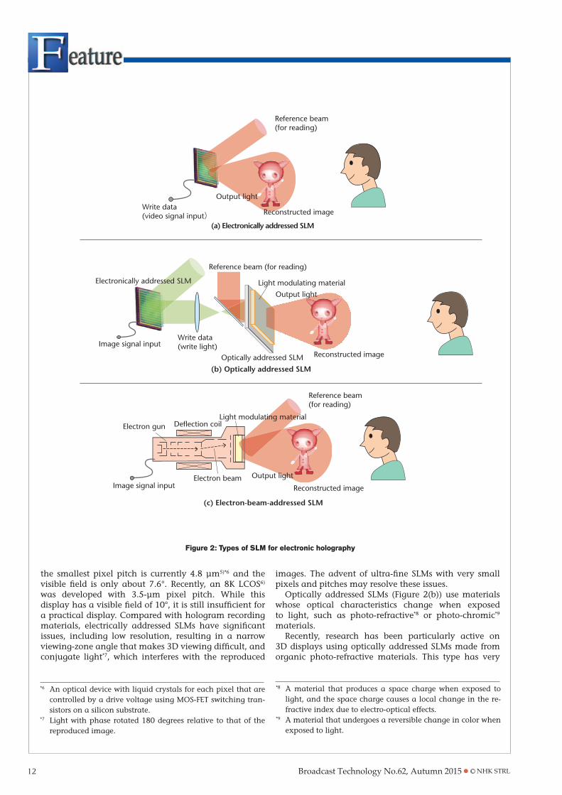
2.2 Features and Issues of SLMs for Holographic DisplaySLMs can be divided into the following three types on
the basis of how they write the information4). i. Electrically addressed SLM: Information corresponding
to the interference pattern in the form of an electrical signal is sent to and “written”, i.e., the SLM changes its characteristics in response, on the SLM.
ii. Optically addressed SLM: The information is written using a laser beam or is an optical image from a compact display device.
iii. Electron-beam-addressed SLM: The information is written using a scanning electron beam in a vacuum.Figure 2 shows three different types of SLM for
electronic holography, and Table 1 lists the features and issues of each. Electrically addressed SLMs (Figure 2(a)) use thin-film transistors (TFTs) or metal-oxide-semiconductor field-effect-transistors (MOS-FETs) to drive the SLM directly. Typical devices are liquid crystal SLMs and digital micro-mirror devices (DMD)*5.
The interference signal is input to these SLMs directly as a video signal, and 3D video can be produced simply by exposing the SLM to light. However, the pixel pitch of these SLMs is currently between 5 and 10 μm, which is not fine enough to display interference patterns at visible light wavelengths (Figure 1). Even when using liquid crystal on silicon (LCOS) technology,
*4 For a wavelength, λ, of 640 nm.
Figure 1: Relationship between pixel pitch and viewing-zone angle (for light wavelength of 640 nm)
Pixel pitch, (µm)
Resolution (lines/mm)
1,000 100
1010.1
60
40
20
0
View
ing-
zone
ang
le,
(d
eg.)
Ψ
*1 Liquid Crystal on Silicon*2 Digital Micro-mirror Device
Hologram recording medium
Spin-SLM
LCOS *1
DMD*2
Table 1: Features and issues of major SLMs for electronic holography
Example device
LCOS, DMD, etc.
Organic photorefractive materials, etc.
EBSLM*, etc.
Type Features Issues
- Electronic signal can be input directly- Motion display possible- Compact (small, lightweight)
- High resolution (1,000 lines/mm or greater)
- Large-size
- Electronic signal can be input directly- Motion display possible
- Increasing resolution (current pixel pitch is 3.5-20 µm)- Increasing screen size
- Equipment such as electronically addressed SLM is needed to form interference pattern, resulting in a large system.
- Motion display
- Increasing resolution (currently 80 lines/mm or less)
- Large-size, because vacuum equipment is required
Electronically addressed SLM
Optically addressedSLM
Electron-beam- addressed SLM
* Electron-beam-addressed SLM
*5 An optical device with 10-μm-square micro-mirrors arranged in an array. Light can be switched ON and OFF by controlling the position of the mirrors.
Broadcast Technology No.62, Autumn 2015 ● C NHK STRL12
the smallest pixel pitch is currently 4.8 μm5)*6 and the visible fi eld is only about 7.6°. Recently, an 8K LCOS6) was developed with 3.5-μm pixel pitch. While this display has a visible fi eld of 10°, it is still insuffi cient for a practical display. Compared with hologram recording materials, electrically addressed SLMs have signifi cant issues, including low resolution, resulting in a narrow viewing-zone angle that makes 3D viewing diffi cult, and conjugate light*7, which interferes with the reproduced
images. The advent of ultra-fi ne SLMs with very small pixels and pitches may resolve these issues.
Optically addressed SLMs (Figure 2(b)) use materials whose optical characteristics change when exposed to light, such as photo-refractive*8 or photo-chromic*9
materials. Recently, research has been particularly active on
3D displays using optically addressed SLMs made from organic photo-refractive materials. This type has very
Figure 2: Types of SLM for electronic holography
Reference beam(for reading)
(c) Electron-beam-addressed SLM
Image signal inputElectron beam
Reconstructed image
Output light
Electron gunLight modulating material
Deflection coil
Reference beam (for reading)
(b) Optically addressed SLM
Image signal inputWrite data(write light)
Reconstructed image
Output lightLight modulating material
Optically addressed SLM
Electronically addressed SLM
Reference beam(for reading)
(a) Electronically addressed SLM
Write data(video signal input) Reconstructed image
Output light
*8 A material that produces a space charge when exposed to light, and the space charge causes a local change in the re-fractive index due to electro-optical effects.
*9 A material that undergoes a reversible change in color when exposed to light.
*6 An optical device with liquid crystals for each pixel that are controlled by a drive voltage using MOS-FET switching tran-sistors on a silicon substrate.
*7 Light with phase rotated 180 degrees relative to that of the reproduced image.
Broadcast Technology No.62, Autumn 2015 ● C NHK STRL 13
promising characteristics compared with electrically addressed SLMs. One is that it is easier to reach a resolution equivalent to that of hologram recording materials because the pixels are not separated. Another is that it is easier to scale the display area because the materials are simply coated on a substrate. The experiments have already been reported on using an optically addressed SLM and the holographic stereogram method*10 to display static images on large-area displays7)8). A major issue with this approach is the method used to input and rewrite the interference pattern. Many experiments using electrically addressed SLMs to produce the interference pattern have been reported, but future developments will depend on whether the requisite number of pixels can be attained. Other issues include the need to supply a separate optical system for high-resolution writing and the resulting increase in system size. Finding a way of displaying video rather than just still images is also a major issue.
In electron-beam-addressed SLMs (Figure 2 (c)), a beam from an electron gun is modulated by an electrical write signal and conventional electro-optic crystals or oil fi lm are used as the optical modulation material9)-11). Experiments in which these devices displayed 2D images holographically have been reported9), but the resolution was inadequate, and the devices were bulky because the method only works in a vacuum.
3. Spin-SLMWe are conducting R&D on an SLM with a huge
number of pixel and a fi ne pixel pitch of 1 μm or less, with the goal of achieving an ideal 3D video display with a wide viewing-zone angle. This new electrically addressed SLM is called a Spin-SLM12), and it is controlled with the
magneto-optic effect*11 and spin transfer switching*12. It has greatly improved viewing characteristics relative to earlier devices.
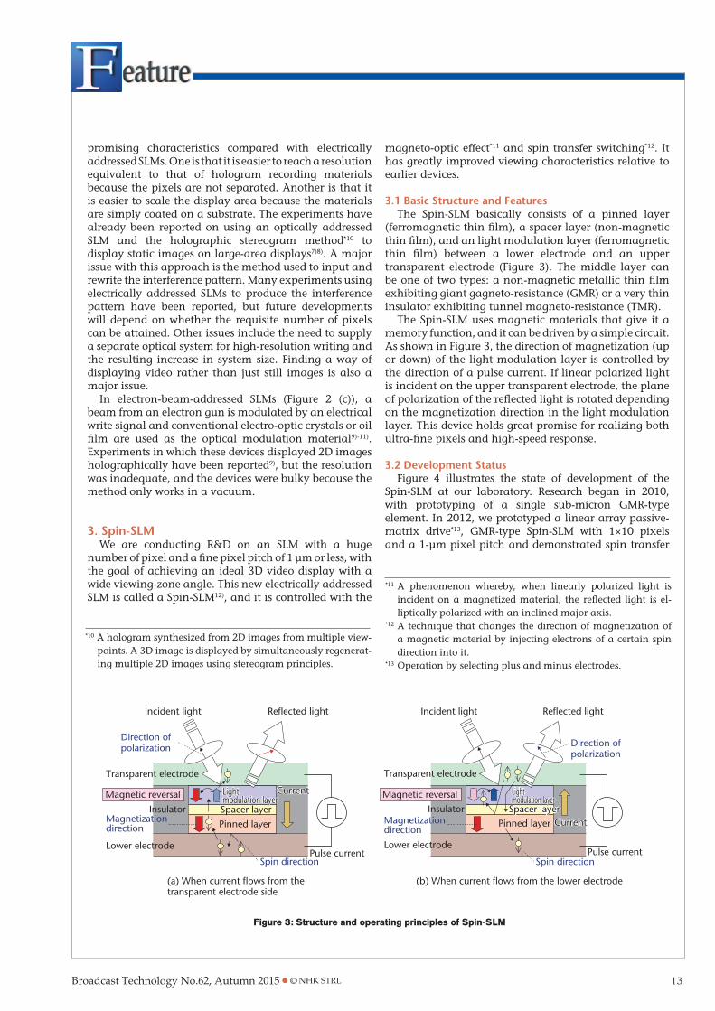
3.1 Basic Structure and Features The Spin-SLM basically consists of a pinned layer
(ferromagnetic thin fi lm), a spacer layer (non-magnetic thin fi lm), and an light modulation layer (ferromagnetic thin fi lm) between a lower electrode and an upper transparent electrode (Figure 3). The middle layer can be one of two types: a non-magnetic metallic thin fi lm exhibiting giant gagneto-resistance (GMR) or a very thin insulator exhibiting tunnel magneto-resistance (TMR).
The Spin-SLM uses magnetic materials that give it a memory function, and it can be driven by a simple circuit. As shown in Figure 3, the direction of magnetization (up or down) of the light modulation layer is controlled by the direction of a pulse current. If linear polarized light is incident on the upper transparent electrode, the plane of polarization of the refl ected light is rotated depending on the magnetization direction in the light modulation layer. This device holds great promise for realizing both ultra-fi ne pixels and high-speed response.
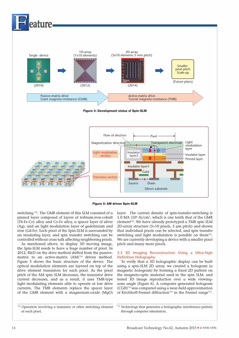
3.2 Development StatusFigure 4 illustrates the state of development of the
Spin-SLM at our laboratory. Research began in 2010, with prototyping of a single sub-micron GMR-type element. In 2012, we prototyped a linear array passive-matrix drive*13, GMR-type Spin-SLM with 1×10 pixels and a 1-μm pixel pitch and demonstrated spin transfer
Figure 3: Structure and operating principles of Spin-SLM
Incident light
Direction of polarization Direction of
polarization
Magnetization direction
Magnetization direction
Spin direction Spin direction
Insulator Insulator
Transparent electrode
Light modulation layer
Light modulation layer
Spacer layer Spacer layer
Pinned layer Pinned layer
Transparent electrode
Magnetic reversal Magnetic reversal
Lower electrode Lower electrode
(a) When current flows from the transparent electrode side
(b) When current flows from the lower electrode
Reflected light
Current
Current
Pulse current Pulse current
Incident light Reflected light
Spacer layer
Light modulation layer
Light modulation layer
Current
Current
*11 A phenomenon whereby, when linearly polarized light is incident on a magnetized material, the refl ected light is el-liptically polarized with an inclined major axis.
*12 A technique that changes the direction of magnetization of a magnetic material by injecting electrons of a certain spin direction into it.
*13 Operation by selecting plus and minus electrodes.
*10 A hologram synthesized from 2D images from multiple view-points. A 3D image is displayed by simultaneously regenerat-ing multiple 2D images using stereogram principles.
Broadcast Technology No.62, Autumn 2015 ● C NHK STRL14
switching 13). The GMR element of this SLM consisted of a pinned layer composed of layers of terbium-iron-cobalt (Tb-Fe-Co) alloy and Co-Fe alloy, a spacer layer of silver (Ag), and an light modulation layer of gadolinium and iron (Gd-Fe). Each pixel of the Spin-SLM is surrounded by an insulating layer, and spin transfer switching can be controlled without cross-talk affecting neighboring pixels.
As mentioned above, to display 3D moving image, the Spin-SLM needs to have a huge number of pixel. In 2012, R&D on the drive method shifted from the passive-matrix to an active-matrix (AM)*14 driven method. Figure 5 shows the basic structure of the device. The optical modulation elements are layered on top of the drive element transistors for each pixel. As the pixel pitch of the AM spin SLM decreases, the transistor drive current decreases, and as a result, it uses TMR-type light modulating elements able to operate at low drive currents. The TMR elements replace the spacer layer of the GMR element with a magnesium-oxide (MgO)
layer. The current density of spin-transfer-switching is 1.0 MA (106 A)/cm2, which is one tenth that of the GMR element14). We have already prototyped a TMR spin SLM 2D-array structure (5×10 pixels, 5 μm pitch) and shown that individual pixels can be selected, and spin transfer switching and light modulation is possible on them15). We are currently developing a device with a smaller pixel pitch and many more pixels.
3.3 3D Imaging Reconstruction Using a Ultra-high Defi nition Holography
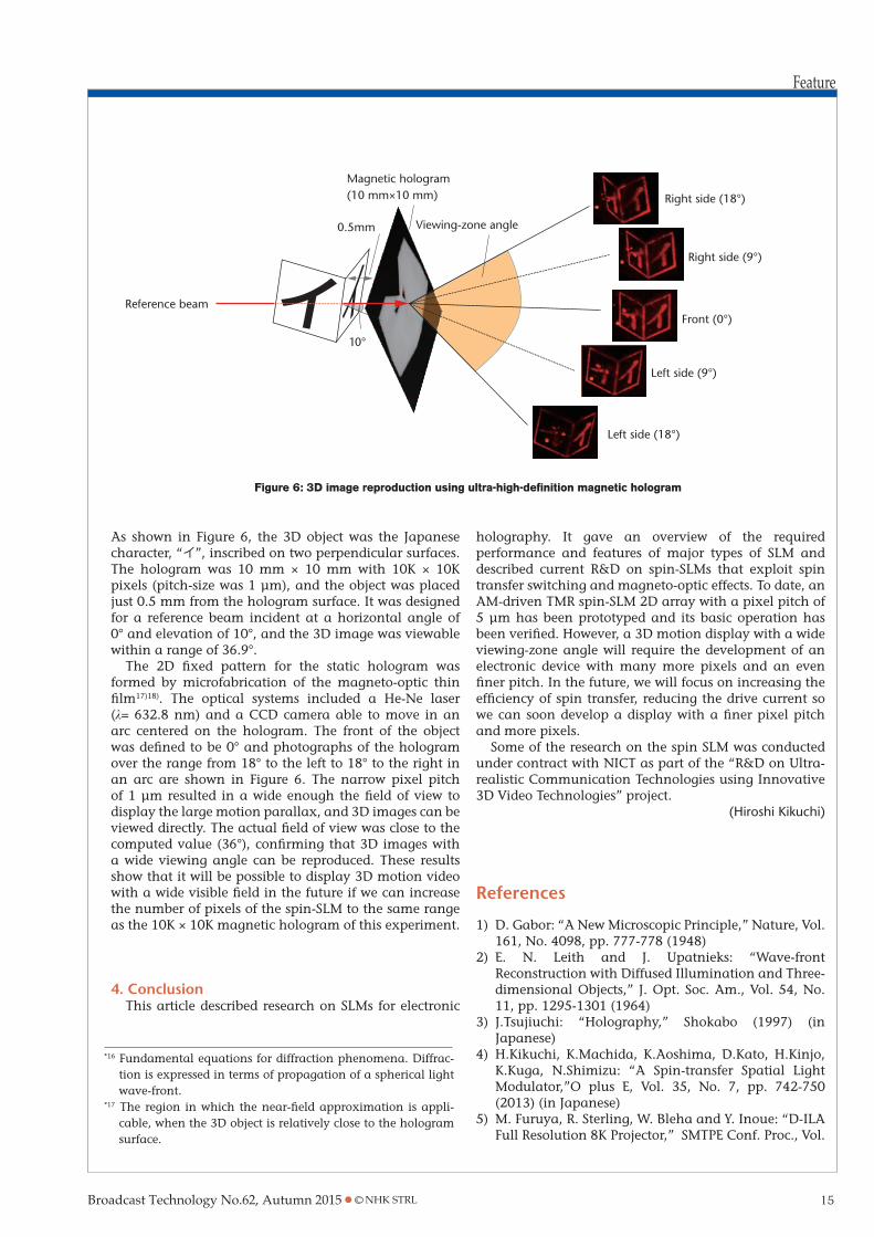
To verify that a 3D holographic display can be built using a spin-SLM 2D array, we created a hologram (a magnetic hologram) by forming a fi xed 2D pattern on the magneto-optic material used in the spin SLM, and tested 3D image reproduction over a wide viewing-zone angle (Figure 6). A computer generated hologram (CGH)*15 was computed using a near-fi eld approximation of Kirchhoff-Fresnel diffraction*16 in the Fresnel range*17.
Figure 5: AM driven Spin-SLM
Transparent electrode Light modulation layer
Insulator layerInsulator
layer2
Insulator layer1
Pinned layer
PixelFlow of electron
Magnetization direction
Gate
Source Drain
Silicon substrate
Light modulation section
Transistor section
Figure 4: Development status of Spin-SLM
Single device
(2010) (2012)
1D-array(1x10 elements)
(Future plans)
Smaller pixel pitchScale-up
Passive-matrix driveGiant magneto-resistance (GMR)
Active-matrix driveTunnel magneto-resistance (TMR)
(2014)
2D-array(5x10 elements�5 mm pitch)
5µm
*15 Technology that generates a holographic interference pattern through computer simulation.
*14 Operation involving a transistor or other switching element at each pixel.
Broadcast Technology No.62, Autumn 2015 ● C NHK STRL
Feature
15
As shown in Figure 6, the 3D object was the Japanese character, “イ”, inscribed on two perpendicular surfaces. The hologram was 10 mm × 10 mm with 10K × 10K pixels (pitch-size was 1 μm), and the object was placed just 0.5 mm from the hologram surface. It was designed for a reference beam incident at a horizontal angle of 0° and elevation of 10°, and the 3D image was viewable within a range of 36.9°.
The 2D fi xed pattern for the static hologram was formed by microfabrication of the magneto-optic thin fi lm17)18). The optical systems included a He-Ne laser (λ= 632.8 nm) and a CCD camera able to move in an arc centered on the hologram. The front of the object was defi ned to be 0° and photographs of the hologram over the range from 18° to the left to 18° to the right in an arc are shown in Figure 6. The narrow pixel pitch of 1 μm resulted in a wide enough the fi eld of view to display the large motion parallax, and 3D images can be viewed directly. The actual fi eld of view was close to the computed value (36°), confi rming that 3D images with a wide viewing angle can be reproduced. These results show that it will be possible to display 3D motion video with a wide visible fi eld in the future if we can increase the number of pixels of the spin-SLM to the same range as the 10K × 10K magnetic hologram of this experiment.
4. ConclusionThis article described research on SLMs for electronic
holography. It gave an overview of the required performance and features of major types of SLM and described current R&D on spin-SLMs that exploit spin transfer switching and magneto-optic effects. To date, an AM-driven TMR spin-SLM 2D array with a pixel pitch of 5 μm has been prototyped and its basic operation has been verifi ed. However, a 3D motion display with a wide viewing-zone angle will require the development of an electronic device with many more pixels and an even fi ner pitch. In the future, we will focus on increasing the effi ciency of spin transfer, reducing the drive current so we can soon develop a display with a fi ner pixel pitch and more pixels.
Some of the research on the spin SLM was conducted under contract with NICT as part of the “R&D on Ultra-realistic Communication Technologies using Innovative 3D Video Technologies” project.
(Hiroshi Kikuchi)
References
1) D. Gabor: “A New Microscopic Principle,” Nature, Vol. 161, No. 4098, pp. 777-778 (1948)
2) E. N. Leith and J. Upatnieks: “Wave-front Reconstruction with Diffused Illumination and Three-dimensional Objects,” J. Opt. Soc. Am., Vol. 54, No. 11, pp. 1295-1301 (1964)
3) J.Tsujiuchi: “Holography,” Shokabo (1997) (in Japanese)
4) H.Kikuchi, K.Machida, K.Aoshima, D.Kato, H.Kinjo, K.Kuga, N.Shimizu: “A Spin-transfer Spatial Light Modulator,”O plus E, Vol. 35, No. 7, pp. 742-750 (2013) (in Japanese)
5) M. Furuya, R. Sterling, W. Bleha and Y. Inoue: “D-ILA Full Resolution 8K Projector,” SMTPE Conf. Proc., Vol.
Figure 6: 3D image reproduction using ultra-high-defi nition magnetic hologram
Reference beam
Magnetic hologram(10 mm×10 mm)
Viewing-zone angle
10°
0.5mm
Right side (18°)
Right side (9°)
Front (0°)
Left side (18°)
Left side (9°)
*16 Fundamental equations for diffraction phenomena. Diffrac-tion is expressed in terms of propagation of a spherical light wave-front.
*17 The region in which the near-fi eld approximation is appli-cable, when the 3D object is relatively close to the hologram surface.

Broadcast Technology No.62, Autumn 2015 ● C NHK STRL16
2009, No. 10, pp. 1-9 (2009)6) NICT Contract research: “2013 Overview of R&D Results
from ‘R&D on an Ultra-high Density High Pixel Count Device for the Ultimate 3D Video Display’,” http://www.nict.go.jp/collabo/commission/k_155.html (in Japanese)
7) P.-A. Blanche, A. Bablumian, R. Voorakaranam, C. Christenson, W. Lin, T. Gu, D. Flores, P. Wang, W.-Y. Hsieh, M. Kathaperumal, B. Rachwal, O. Siddiqui, J. Thomas, R. A. Norwood, M. Yamamoto and N. Peyghambarian: “Holographic Three-dimensional Telepresence Using Large-area Photorefractive Polymer,” Nature, Vol. 468, No. 7320, pp. 80-83 (2010)
8) N. Tsutsumi, K. Kinashi, K. Tada, K. Fukuzawa and Y. Kawabe: “Fully Updatable Three dimensional Holographic Stereogram Display Device Based on Organic Monolithic Compound,” Opt. Express, Vol. 21, No. 17, 19880-19884 (2013)
9) T.-C. Poon, B. W. Schilling, M. H. Wu, K. Shinoda and Y. Suzuki: “Real-time Two dimensional Holographic Imaging by Using an Electron-beam-addressed Spatial Light Modulator,” Opt. Lett., Vol. 18, No. 1, pp. 63-65 (1993)
10) E. Baumann: “The Fischer Large-Screen Projection System,” SMPTE J., Vol. 60, No. 4, pp. 344-356 (1953)
11) W. E. Glenn: “Principles of Simultaneous-Color Projection Television Using Fluid Deformation,” SMPTE J., Vol. 79, No. 11, pp. 788-794 (1970)
12) NHK STRL R&D: “Special Feature on Basic Holography Technologies,” No. 138 (2013) (in Japanese)
13) K. Aoshima, K. Machida, D. Kato, T. Mishina, K. Wada, Y.-Fu Cai, H. Kinjo, K. Kuga, H. Kikuchi, T. Ishibashi and N. Shimizu: “A Magneto-Optical Spatial Light Modulator Driven by Spin Transfer Switching for 3D Holography Applications,” J. Display Technol., Vol. 11, No. 2, pp. 129-135 (2015)
14) H. Kinjo, K. Machida, S. Matsui, K. Aoshima, D. Kato, K. Kuga, H. Kikuchi and N. Shimizu: “Low-current-density Spin-transfer Switching in Gd22Fe78-MgO Magnetic Tunnel Junction,” J. Appl. Phys., Vol. 115, No. 20, pp. 203903.1-3 (2014)
15) K. Aoshima, H. Kinjo, K. Machida, D. Kato, K. Kuga, H. Kikuchi and N. Shimizu: “Magneto-Optical Spatial Light Modulator Driven by Si Based MOS-FET Backplane for Holography Display,” Proc. IDW 2014, MEET3-5L (2014)
16) T. Mishina, F. Okano and I. Yuyama: “Time-alternating Method Based on Single-sideband Holography with Half-zone-plate Processing for the Enlargement of Viewing Zones,” Appl. Opt., Vol. 38, No. 17, pp. 3703-3713 (1999)
17) D. Kato, K. Aoshima, K. Machida, A. Emoto, H. Kinjo, K. Kuga, H. Ono, T. Ishibashi, H. Kikuchi and N. Shimizu: “Holographic Images Reconstructed from GMR-based Fringe Pattern,” EPJ Web of Conf., Vol. 40, pp. 16006.1-4 (2013)
18) K. Machida, D. Kato, T. Mishina, H. Kinjo, K. Aoshima, K. Kuga, H. Kikuchi and N. Shimizu: “Three-Dimensional Image Reconstruction with a Wide Viewing-Zone-Angle Using a GMR Based Hologram,” OSA Topical Meeting Digital Holography and 3-D Imaging (DH), DTh2A.5(2013)