Embed Size (px)
Citation preview
Prof. Phil Allen (2/16/00) Page 1
Georgia Tech, School of ECE
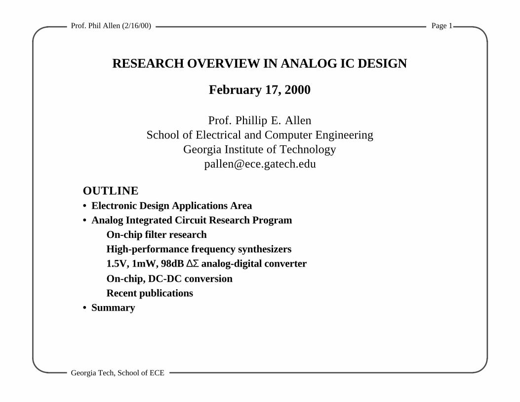
RESEARCH OVERVIEW IN ANALOG IC DESIGN
February 17, 2000
Prof. Phillip E. AllenSchool of Electrical and Computer Engineering
Georgia Institute of [email protected]
OUTLINE• Electronic Design Applications Area• Analog Integrated Circuit Research Program
On-chip filter researchHigh-performance frequency synthesizers1.5V, 1mW, 98dB ∆Σ analog-digital converterOn-chip, DC-DC conversionRecent publications
• Summary
Prof. Phil Allen (2/16/00) Page 2
Georgia Tech, School of ECE
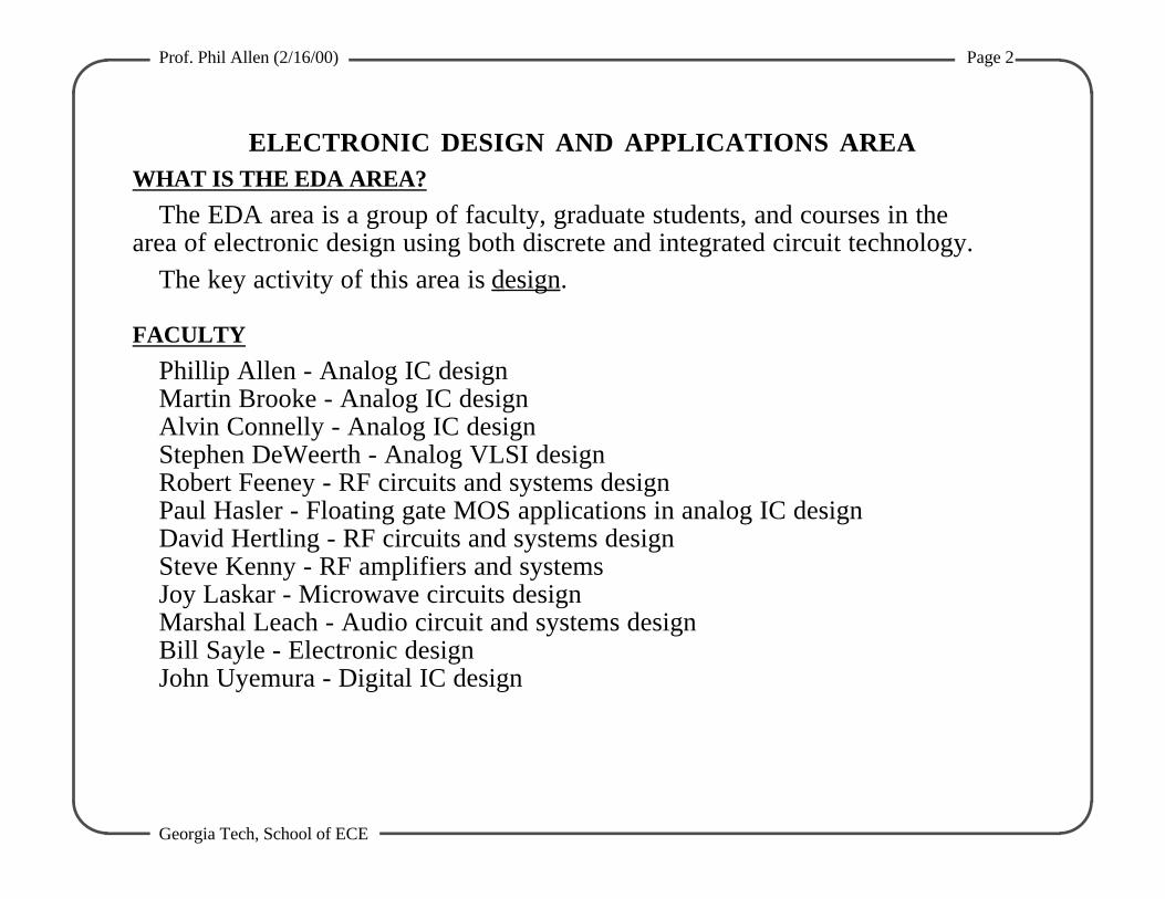
ELECTRONIC DESIGN AND APPLICATIONS AREAWHAT IS THE EDA AREA?
The EDA area is a group of faculty, graduate students, and courses in thearea of electronic design using both discrete and integrated circuit technology.
The key activity of this area is design .
FACULTY
Phillip Allen - Analog IC designMartin Brooke - Analog IC designAlvin Connelly - Analog IC designStephen DeWeerth - Analog VLSI designRobert Feeney - RF circuits and systems designPaul Hasler - Floating gate MOS applications in analog IC designDavid Hertling - RF circuits and systems designSteve Kenny - RF amplifiers and systemsJoy Laskar - Microwave circuits designMarshal Leach - Audio circuit and systems designBill Sayle - Electronic designJohn Uyemura - Digital IC design
Prof. Phil Allen (2/16/00) Page 3
Georgia Tech, School of ECE
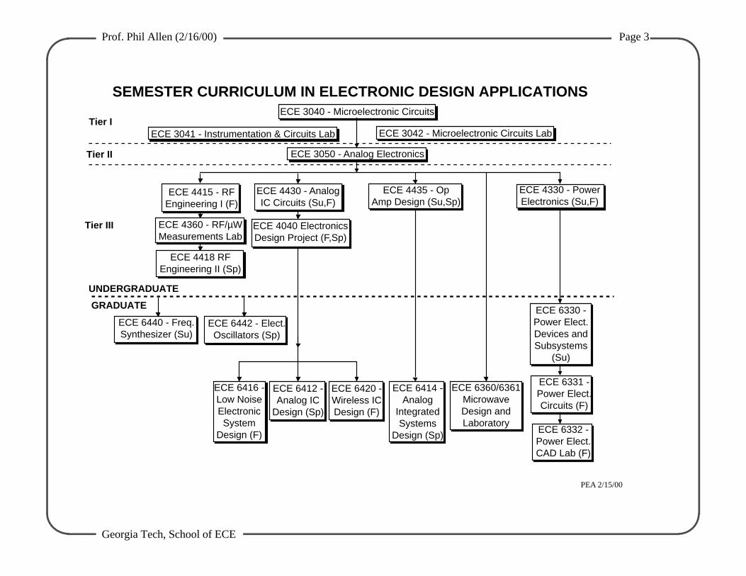
SEMESTER CURRICULUM IN ELECTRONIC DESIGN APPLICATIONSECE 3040 - Microelectronic Circuits
ECE 3041 - Instrumentation & Circuits Lab ECE 3042 - Microelectronic Circuits Lab
ECE 3050 - Analog Electronics
ECE 4415 - RFEngineering I (F)
ECE 4360 - RF/µWMeasurements Lab
ECE 4418 RFEngineering II (Sp)
ECE 4430 - AnalogIC Circuits (Su,F)
ECE 4040 ElectronicsDesign Project (F,Sp)
ECE 4435 - OpAmp Design (Su,Sp)
ECE 4330 - PowerElectronics (Su,F)
UNDERGRADUATE
GRADUATE
ECE 6440 - Freq.Synthesizer (Su)
ECE 6442 - Elect.Oscillators (Sp)
ECE 6416 - Low Noise Electronic System
Design (F)
ECE 6412 - Analog IC
Design (Sp)
ECE 6420 -Wireless ICDesign (F)
ECE 6414 -Analog
IntegratedSystems
Design (Sp)
ECE 6360/6361MicrowaveDesign and Laboratory
ECE 6330 -Power Elect.Devices andSubsystems
(Su)
ECE 6331 -Power Elect.Circuits (F)
ECE 6332 -Power Elect.CAD Lab (F)
Tier I
Tier II
Tier III
PEA 2/15/00
Prof. Phil Allen (2/16/00) Page 4
Georgia Tech, School of ECE
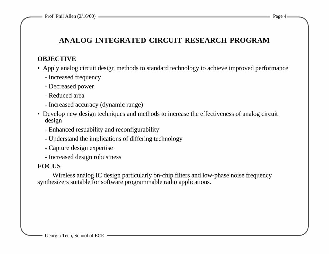
ANALOG INTEGRATED CIRCUIT RESEARCH PROGRAM
OBJECTIVE• Apply analog circuit design methods to standard technology to achieve improved performance
- Increased frequency- Decreased power- Reduced area- Increased accuracy (dynamic range)
• Develop new design techniques and methods to increase the effectiveness of analog circuitdesign- Enhanced resuability and reconfigurability- Understand the implications of differing technology- Capture design expertise- Increased design robustness
FOCUSWireless analog IC design particularly on-chip filters and low-phase noise frequency
synthesizers suitable for software programmable radio applications.
Prof. Phil Allen (2/16/00) Page 5
Georgia Tech, School of ECE
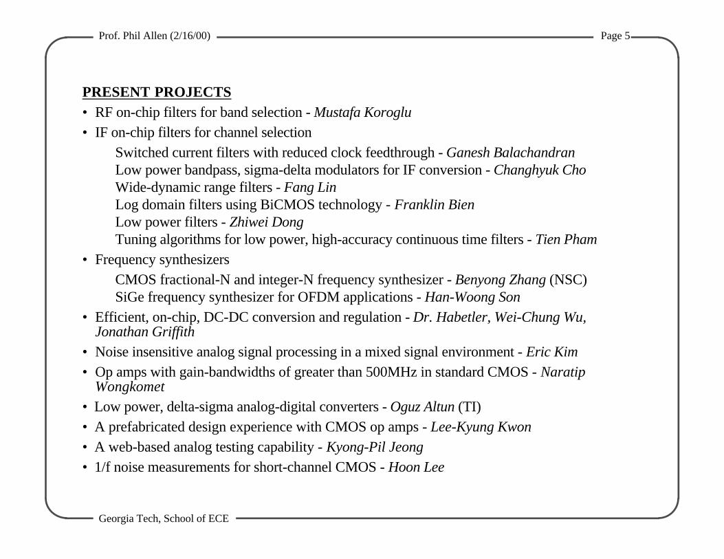
PRESENT PROJECTS• RF on-chip filters for band selection - Mustafa Koroglu• IF on-chip filters for channel selection
Switched current filters with reduced clock feedthrough - Ganesh BalachandranLow power bandpass, sigma-delta modulators for IF conversion - Changhyuk ChoWide-dynamic range filters - Fang LinLog domain filters using BiCMOS technology - Franklin BienLow power filters - Zhiwei DongTuning algorithms for low power, high-accuracy continuous time filters - Tien Pham
• Frequency synthesizersCMOS fractional-N and integer-N frequency synthesizer - Benyong Zhang (NSC)SiGe frequency synthesizer for OFDM applications - Han-Woong Son
• Efficient, on-chip, DC-DC conversion and regulation - Dr. Habetler, Wei-Chung Wu,Jonathan Griffith
• Noise insensitive analog signal processing in a mixed signal environment - Eric Kim• Op amps with gain-bandwidths of greater than 500MHz in standard CMOS - Naratip
Wongkomet• Low power, delta-sigma analog-digital converters - Oguz Altun (TI)• A prefabricated design experience with CMOS op amps - Lee-Kyung Kwon• A web-based analog testing capability - Kyong-Pil Jeong• 1/f noise measurements for short-channel CMOS - Hoon Lee
Prof. Phil Allen (2/16/00) Page 6
Georgia Tech, School of ECE
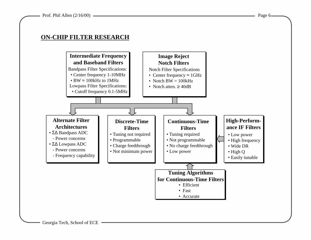
ON-CHIP FILTER RESEARCH
Discrete-TimeFilters
• Tuning not required• Programmable• Charge feedthrough• Not minimum power
Continuous-TimeFilters
• Tuning required• Not programmable• No charge feedthrough• Low power
Alternate FilterArchitectures
• Σ∆ Bandpass ADC - Power concerns• Σ∆ Lowpass ADC - Power concerns - Frequency capability
Tuning Algorithmsfor Continuous-Time Filters
Intermediate Frequencyand Baseband Filters
Bandpass Filter Specifications: • Center frequency 1-10MHz • BW ≈ 100kHz to 1MHzLowpass Filter Specifications: • Cutoff frequency 0.1-5MHz
Image RejectNotch Filters
Notch Filter Specifications• Center frequency ≈ 1GHz• Notch BW = 100kHz• Notch atten. ≥ 40dB
• Efficient• Fast• Accurate
High-Perform-ance IF Filters• Low power• High frequency• Wide DR• High Q• Easily tunable
Prof. Phil Allen (2/16/00) Page 7
Georgia Tech, School of ECE
REVIEW OF SOME ON-CHIP FILTER RESEARCH PROGRESS
• On-Chip Image-Reject Filters - Mustafa Koroglu• Improved Memory Cells for Switched-Current Filters - Ganesh Balachandran• Low Power Baseband Filters - Zhiwei Dong• Tuning Algorithms for Continuous Time Filters - Tien Pham
On-chip Image-reject Filter 01/20/00
2
re
l NF
ques are employed
OutDemodulator
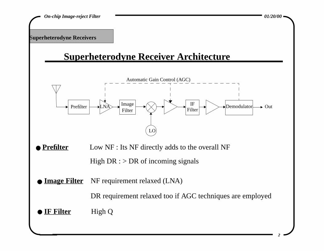
Superheterodyne Receivers
Superheterodyne Receiver Architectu
Prefilter Low NF : Its NF directly adds to the overal
High DR : > DR of incoming signals
Image Filter NF requirement relaxed (LNA)
DR requirement relaxed too if AGC techni
IF Filter High Q
Prefilter LNA ImageFilter
LO
FilterIF
Automatic Gain Control (AGC)
On-chip Image-reject Filter 01/20/00
3
ions)
pression
filter are noisy)
ion!
LO feedthrough dc offset.
Superheterodyne Receivers
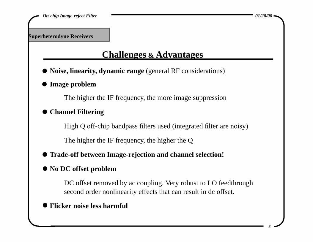
Challenges & Advantages
Noise, linearity, dynamic range (general RF considerat
Image problem
The higher the IF frequency, the more image sup
Channel Filtering
High Q off-chip bandpass filters used (integrated
The higher the IF frequency, the higher the Q
Trade-off between Image-rejection and channel select
No DC offset problem
DC offset removed by ac coupling. Very robust tosecond order nonlinearity effects that can result in
Flicker noise less harmful
On-chip Image-reject Filter 01/20/00
4
nductors
ixer)
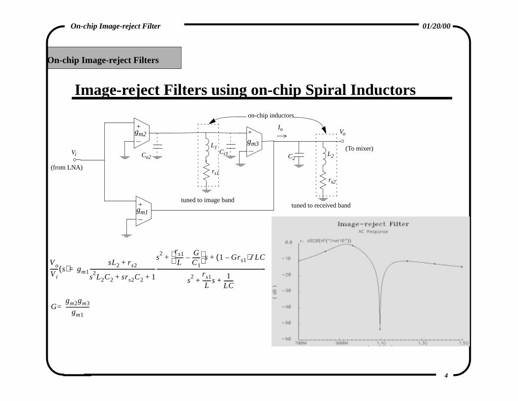
On-chip Image-reject Filters
Image-reject Filters using on-chip Spiral I
+gm2_
L1
rs1
+gm1_
Vi
VoIo
Co2Ci3
gm3_
+
L2
rs2
C2
(from LNA)
(To m
on-chip inductors
tuned to received bandtuned to image band
Vo
Vi------ s( ) gm1
sL2 r s2+
s2L2C2 srs2C2 1+ +
--------------------------------------------------
s2 r s1
L------ G
C1------–
s 1 Grs1–( ) LC⁄+ +
s2 r s1
L------s 1
LC-------+ +
-----------------------------------------------------------------------------------=
Ggm2gm3
gm1------------------=
On-chip Image-reject Filter 01/20/00
5
a PLL, VCO frequency is
llation amplitude by
rs with Q of 6 and 6
r 40dB, 1% required)
On-chip Image-reject Filters
Challenges & Benefits
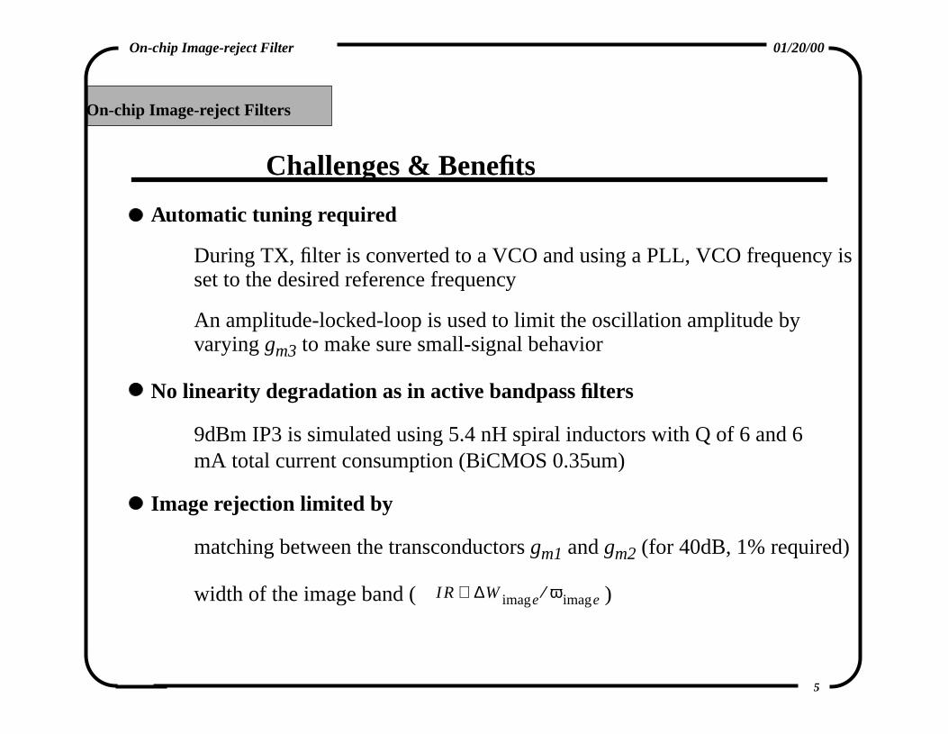
Automatic tuning required
During TX, filter is converted to a VCO and usingset to the desired reference frequency
An amplitude-locked-loop is used to limit the oscivaryinggm3 to make sure small-signal behavior
No linearity degradation as in active bandpass filters
9dBm IP3 is simulated using 5.4 nH spiral inductomA total current consumption (BiCMOS 0.35um)
Image rejection limited by
matching between the transconductorsgm1 andgm2 (fo
width of the image band ( )IR ∆W eimag ω eimag⁄∝
On-chip Image-reject Filter 01/20/00
6
uitry
o mixer)
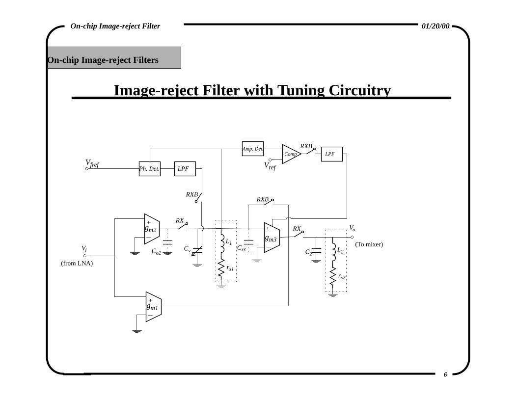
On-chip Image-reject Filters
Image-reject Filter with Tuning Circ
+gm2_
L1
rs1
Cv
+gm1_
Vi
Vo
Co2Ci3
gm3_
+
L2
rs2
C2
(from LNA)
(T
RXRX
RXB
Amp. Det.Comp LPF
RXB
Ph. Det. LPF
RXB
Vfref Vref
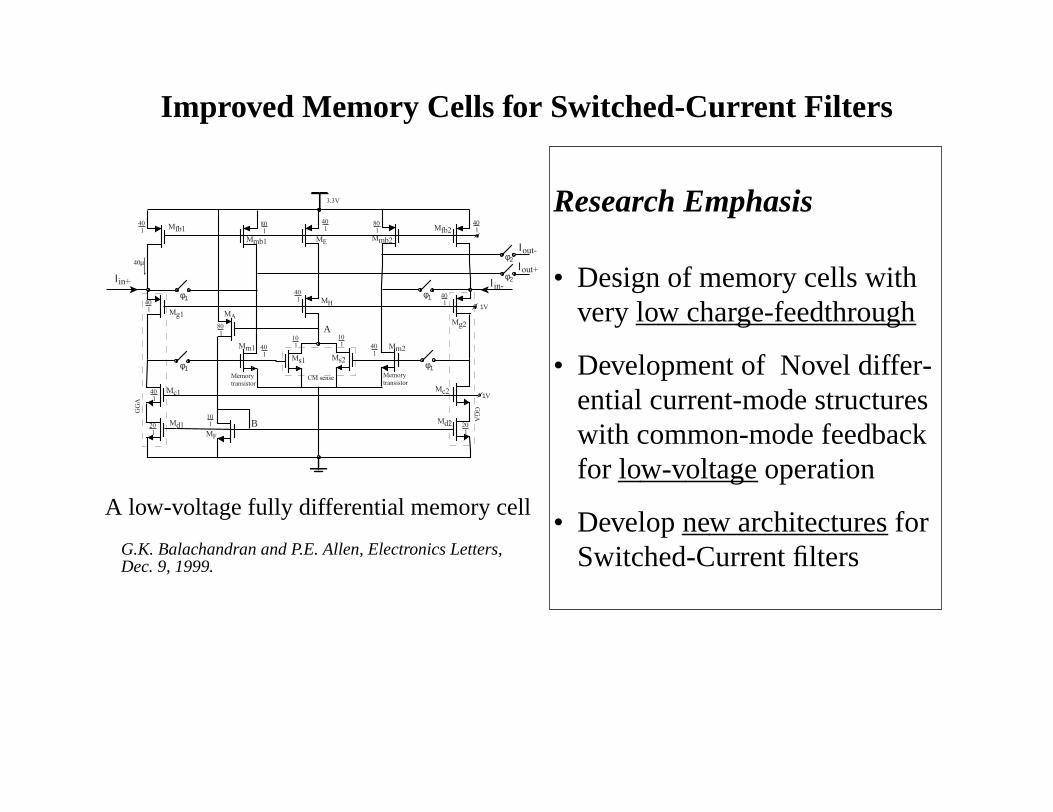
Improved Memory Cells for Switched-Current Filters
Research Emphasis
• Design of memory cells withvery low charge-feedthrough
• Development of Novel differ-ential current-mode structureswith common-mode feedbackfor low-voltage operation
• Developnew architectures forSwitched-Current filters
φ1
φ2Ιin-
φ2
Ιout-Ιout+
Mfb2Mmb2
Mg2
Mm2Mm1
φ1
Ιin+
Mfb1
Mmb1
Mg1 MA
Memory
transistor
GGA
φ1
Mc2
Md2
φ1
Mc1
Md1
Memory
transistor
Ms1 Ms2
CM sense
ME
MH
MF
401
401
401
801
801
401
401
401
101
101 40
1401
401
201
201
801
101
3.3V
40µ
1V
1V
A
B
GGA
A low-voltage fully differential memory cell
G.K. Balachandran and P.E. Allen, Electronics Letters,Dec. 9, 1999.
The Analysis of low power filters
2
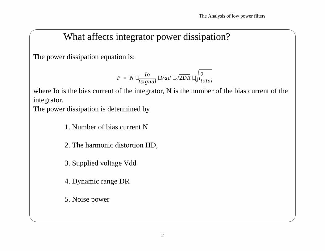
What affects integrator power dissipation?
The power dissipation equation is:
where Io is the bias current of the integrator, N is the number of the bias current of theintegrator.The power dissipation is determined by
1. Number of bias current N
2. The harmonic distortion HD,
3. Supplied voltage Vdd
4. Dynamic range DR
5. Noise power
P NIo
Isignal------------------ Vdd 2DR itotal
2⋅ ⋅⋅⋅=
The Analysis of low power filters
3
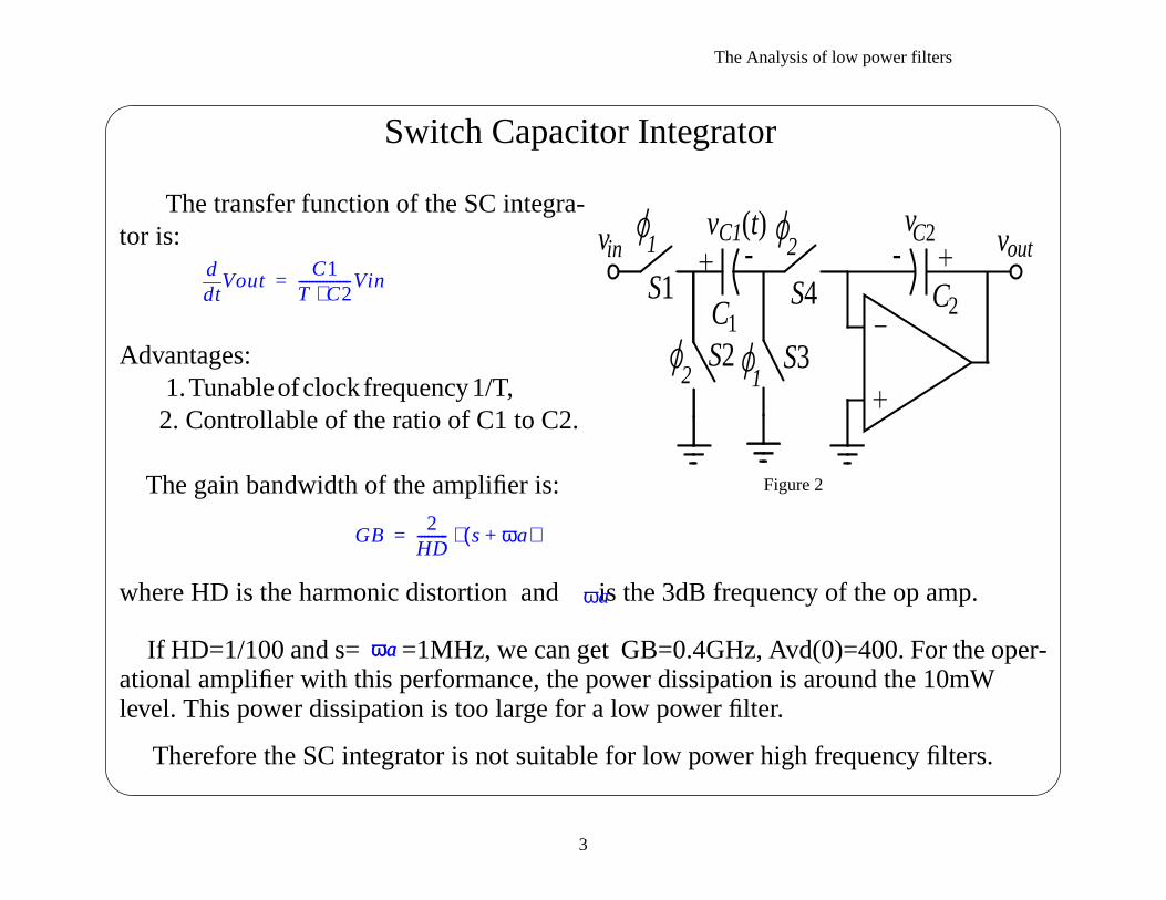
Switch Capacitor Integrator
The transfer function of the SC integra-tor is:
Advantages:1.Tunableofclock frequency1/T,
2. Controllable of the ratio of C1 to C2.
The gain bandwidth of the amplifier is:
where HD is the harmonic distortion and is the 3dB frequency of the op amp.
If HD=1/100 and s= =1MHz, we can get GB=0.4GHz, Avd(0)=400. For the oper-ational amplifier with this performance, the power dissipation is around the 10mWlevel. This power dissipation is too large for a low power filter.
Therefore the SC integrator is not suitable for low power high frequency filters.
tdd
VoutC1
T C2⋅---------------Vin=
GB2
HD--------- s ωa+( )⋅=
ωa
ωaωa
1 2
2C
voutinv vC2+-
12
1C
vC1(t)
+-
+ -S1
S2 S3
S4
Figure 2
The Analysis of low power filters
4
Gm-C Integrator
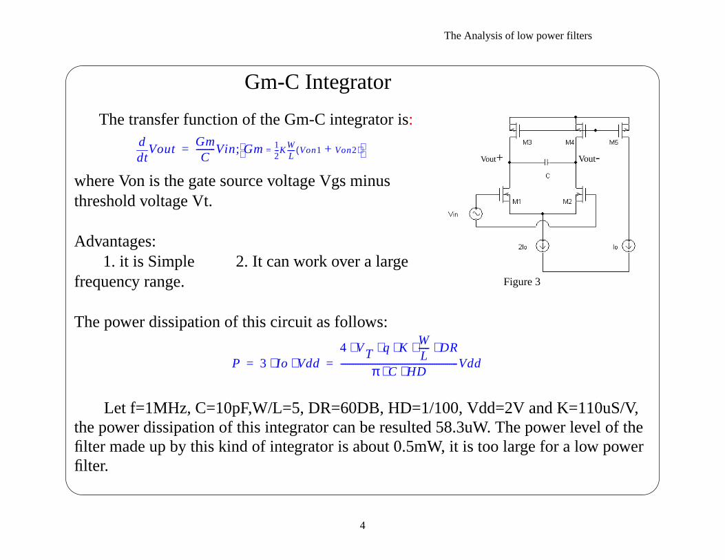
The transfer function of the Gm-C integrator is:
where Von is the gate source voltage Vgs minusthreshold voltage Vt.
Advantages: 1. it is Simple 2. It can work over a largefrequency range.
The power dissipation of this circuit as follows:
Let f=1MHz, C=10pF,W/L=5, DR=60DB, HD=1/100, Vdd=2V and K=110uS/V,the power dissipation of this integrator can be resulted 58.3uW. The power level of thefilter made up by this kind of integrator is about 0.5mW, it is too large for a low powerfilter.
tdd
VoutGmC
---------Vin Gm 12---K
WL----- Von1 Von2+( )=
;=
P 3 Io Vdd⋅ ⋅4 V⋅ T q K
WL----- DR⋅ ⋅ ⋅ ⋅
π C HD⋅⋅-------------------------------------------------------Vdd= =
Vout+ Vout-
Figure 3
The Analysis of low power filters
5
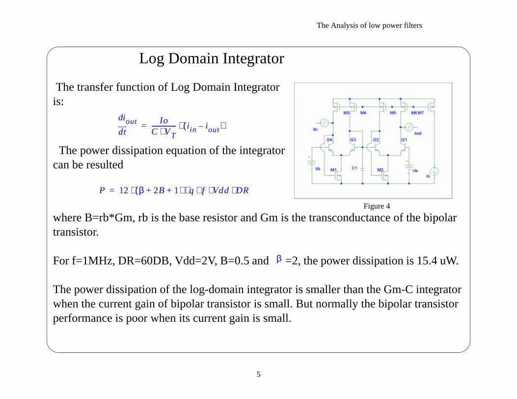
Log Domain Integrator
The transfer function of Log Domain Integratoris:
The power dissipation equation of the integratorcan be resulted
where B=rb*Gm, rb is the base resistor and Gm is the transconductance of the bipolartransistor.
For f=1MHz, DR=60DB, Vdd=2V, B=0.5 and =2, the power dissipation is 15.4 uW.
The power dissipation of the log-domain integrator is smaller than the Gm-C integratorwhen the current gain of bipolar transistor is small. But normally the bipolar transistorperformance is poor when its current gain is small.
td
diout IoC VT⋅---------------- i in iout–( )⋅=
P 12 β 2B 1+ +( ) q f Vdd DR⋅⋅ ⋅ ⋅ ⋅=
Figure 4
β
Prof. Phil Allen (2/16/00) Page 10
Georgia Tech, School of ECE
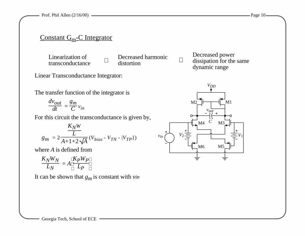
Constant G m -C Integrator
Linearization oftransconductance ⇒ Decreased harmonic
distortion ⇒Decreased powerdissipation for the samedynamic range
Linear Transconductance Integrator:
The transfer function of the integrator isdvout
dt = gmC vin
For this circuit the transconductance is given by,
gm = 2·
KNW
LA+1+2· A
(Vbias - VTN - |VTP})
where A is defined from
KNWNLN
= A
KPWP
LP
It can be shown that gm is constant with vin
vout
VDD
M2 M1
CM4 M3
V2 V1
M6 M5
vin
The Analysis of low power filters
7
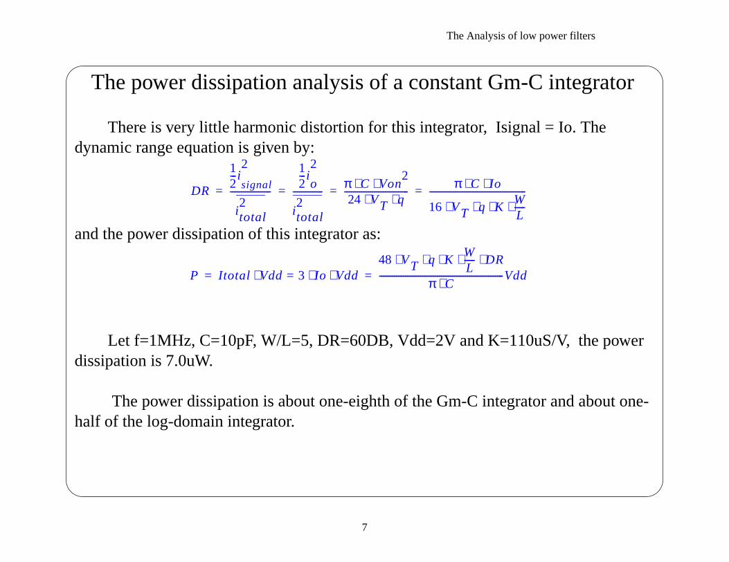
The power dissipation analysis of a constant Gm-C integrator
There is very little harmonic distortion for this integrator, Isignal = Io. Thedynamic range equation is given by:
and the power dissipation of this integrator as:
Let f=1MHz, C=10pF, W/L=5, DR=60DB, Vdd=2V and K=110uS/V, the powerdissipation is 7.0uW.
The power dissipation is about one-eighth of the Gm-C integrator and about one-half of the log-domain integrator.
DR
12--- i
signal
2
i total2
-------------------
12--- i
o
2
i total2
-------------- π C Von2⋅ ⋅
24 VT q⋅ ⋅------------------------------ π C Io⋅ ⋅
16 VT q KWL-----⋅ ⋅ ⋅ ⋅
---------------------------------------------= = = =
P Itotal Vdd⋅ 3= Io Vdd⋅ ⋅48 V⋅ T q K
WL----- DR⋅ ⋅ ⋅ ⋅
π C⋅----------------------------------------------------------Vdd= =
The Analysis of low power filters
8
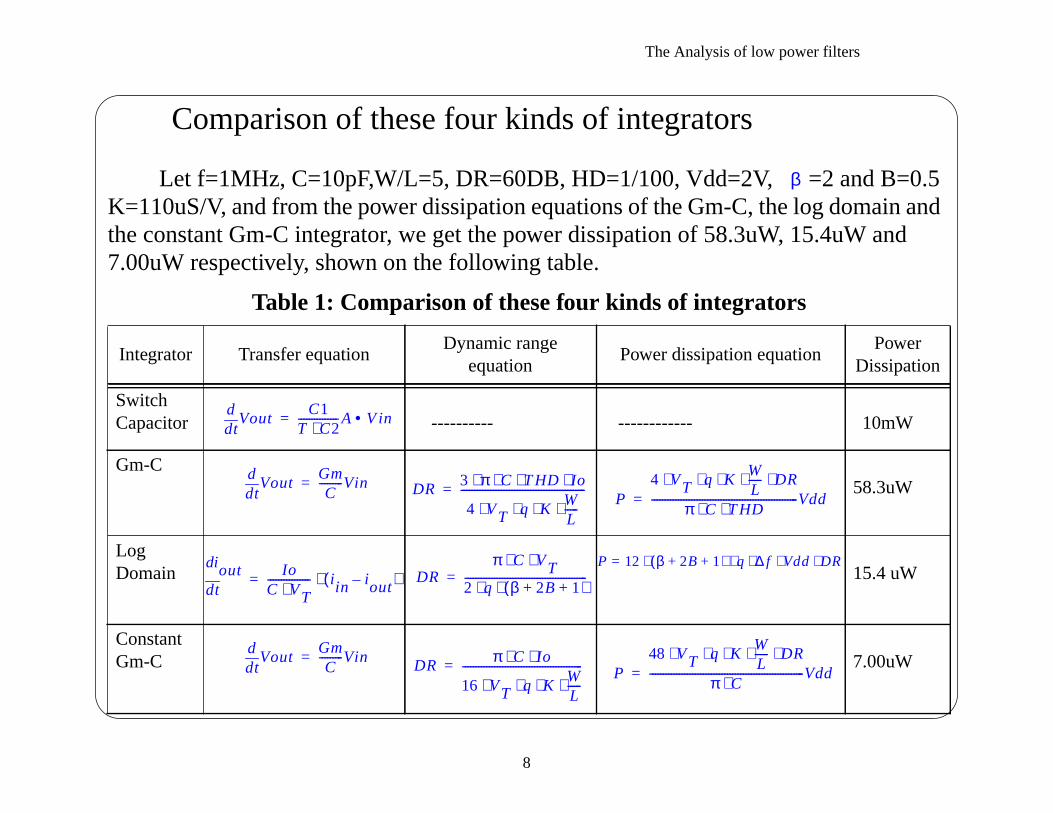
Comparison of these four kinds of integrators
Let f=1MHz, C=10pF,W/L=5, DR=60DB, HD=1/100, Vdd=2V, =2 and B=0.5K=110uS/V, and from the power dissipation equations of the Gm-C, the log domain andthe constant Gm-C integrator, we get the power dissipation of 58.3uW, 15.4uW and7.00uW respectively, shown on the following table.
Table 1: Comparison of these four kinds of integrators
Integrator Transfer equationDynamic range
equationPower dissipation equation
PowerDissipation
SwitchCapacitor ---------- ------------ 10mW
Gm-C58.3uW
LogDomain 15.4 uW
ConstantGm-C 7.00uW
tdd
VoutC1
T C2⋅---------------A V• in=
tdd
VoutGmC
---------Vin= DR3 π C T⋅ HD Io⋅ ⋅ ⋅
4 VT q KWL-----⋅ ⋅ ⋅ ⋅
-----------------------------------------------=P
4 V⋅ T q KWL----- DR⋅ ⋅ ⋅ ⋅
π C T⋅ HD⋅-------------------------------------------------------Vdd=
td
diout IoC VT⋅---------------- i in iout–( )⋅= DR
π C VT⋅ ⋅
2 q β 2B 1+ +( )⋅ ⋅----------------------------------------------=
P 12= β 2B 1+ +( ) q f∆ Vdd DR⋅⋅ ⋅ ⋅ ⋅
tdd
VoutGmC
---------Vin= DRπ C Io⋅ ⋅
16 VT q KWL-----⋅ ⋅ ⋅ ⋅
---------------------------------------------= P48 V⋅ T q K
WL----- DR⋅ ⋅ ⋅ ⋅
π C⋅----------------------------------------------------------Vdd=
β
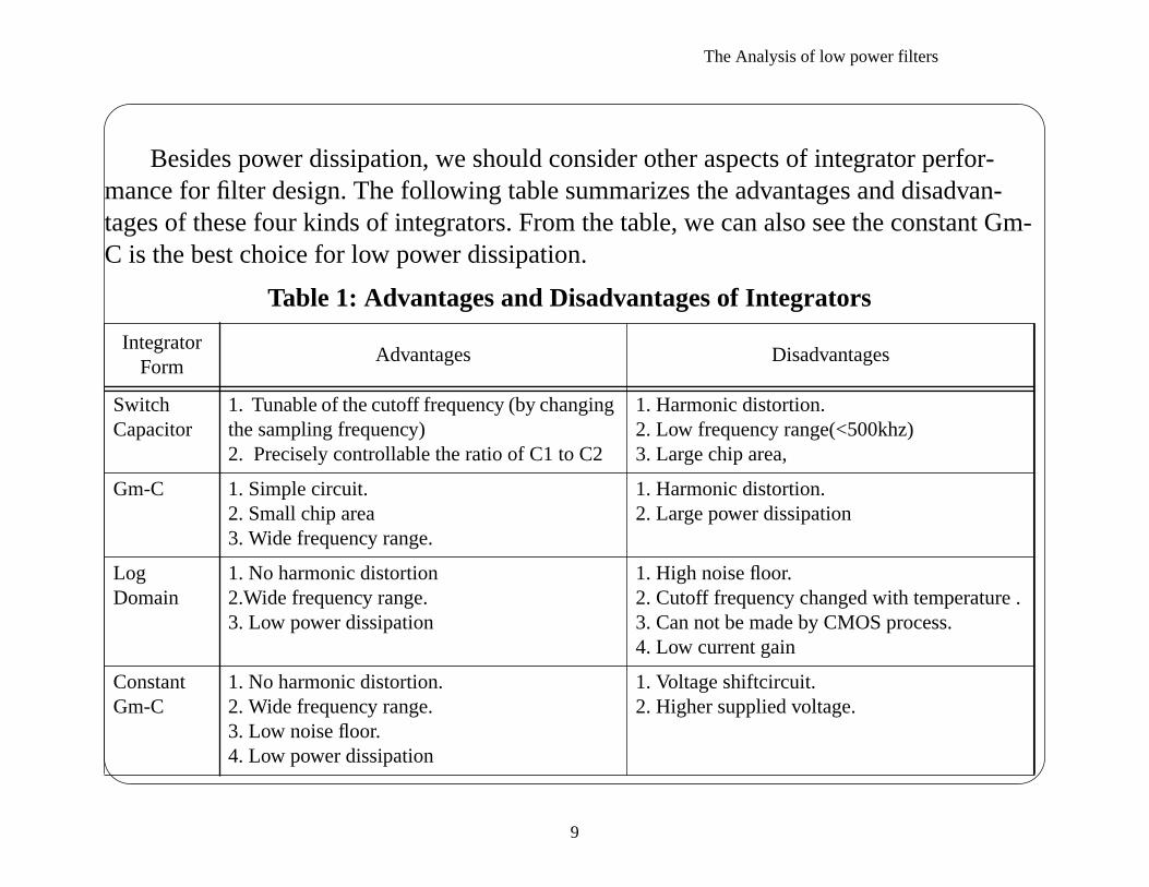
The Analysis of low power filters
9
Besides power dissipation, we should consider other aspects of integrator perfor-mance for filter design. The following table summarizes the advantages and disadvan-tages of these four kinds of integrators. From the table, we can also see the constant Gm-C is the best choice for low power dissipation.
Table 1: Advantages and Disadvantages of Integrators
IntegratorForm
Advantages Disadvantages
SwitchCapacitor
1. Tunable of the cutoff frequency (by changingthe sampling frequency)2. Precisely controllable the ratio of C1 to C2
1. Harmonic distortion.2. Low frequency range(<500khz)3. Large chip area,
Gm-C 1. Simple circuit.2. Small chip area3. Wide frequency range.
1. Harmonic distortion.2. Large power dissipation
LogDomain
1. No harmonic distortion2.Wide frequency range.3. Low power dissipation
1. High noise floor.2. Cutoff frequency changed with temperature .3. Can not be made by CMOS process.4. Low current gain
ConstantGm-C
1. No harmonic distortion.2. Wide frequency range.3. Low noise floor.4. Low power dissipation
1. Voltage shiftcircuit.2. Higher supplied voltage.
The Analysis of low power filters
10
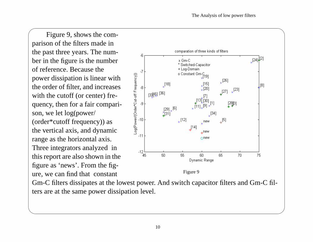
Figure 9, shows the com-parison of the filters made inthe past three years. The num-ber in the figure is the numberof reference. Because thepower dissipation is linear withthe order of filter, and increaseswith the cutoff (or center) fre-quency, then for a fair compari-son, we let log(power/(order*cutoff frequency)) asthe vertical axis, and dynamicrange as the horizontal axis.Three integrators analyzed inthis report are also shown in thefigure as ‘news’. From the fig-ure, we can find that constantGm-C filters dissipates at the lowest power. And switch capacitor filters and Gm-C fil-ters are at the same power dissipation level.
Figure 9
Prof. Phil Allen (2/16/00) Page 11
Georgia Tech, School of ECE
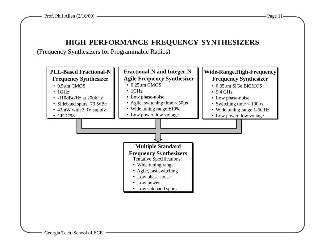
HIGH PERFORMANCE FREQUENCY SYNTHESIZERS(Frequency Synthesizers for Programmable Radios)
Multiple Standard Frequency Synthesizers
Tentative Specifications:• Wide tuning range• Agile, fast switching• Low phase-noise• Low power• Low sideband spurs
PLL-Based Fractional-N Frequency Synthesizer • 0.5µm CMOS• 1GHz• -110dBc/Hz at 200kHz• Sideband spurs -73.5dBc• 43mW with 3.3V supply• CICC'98
Fractional-N and Integer-NAgile Frequency Synthesizer
• 0.25µm CMOS• 1GHz• Low phase-noise• Agile, switching time < 50µs• Wide tuning range ±10%• Low power, low voltage
Wide-Range,High-Frequency Frequency Synthesizer• 0.35µm SiGe BiCMOS• 5.4 GHz• Low phase-noise• Switching time < 100µs• Wide tuning range 1-6GHz• Low power, low voltage
Prof. Phil Allen (2/16/00) Page 12
Georgia Tech, School of ECE
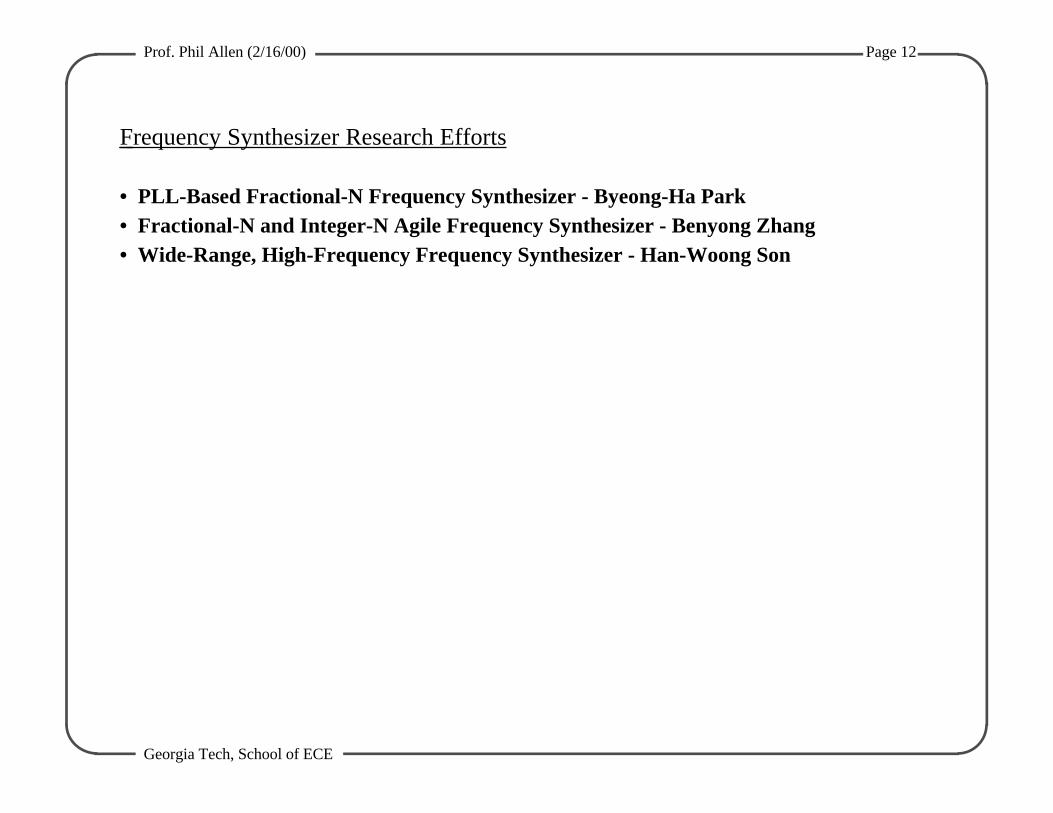
Frequency Synthesizer Research Efforts
• PLL-Based Fractional-N Frequency Synthesizer - Byeong-Ha Park• Fractional-N and Integer-N Agile Frequency Synthesizer - Benyong Zhang• Wide-Range, High-Frequency Frequency Synthesizer - Han-Woong Son
Prof. Phil Allen (2/16/00) Page 13
Georgia Tech, School of ECE
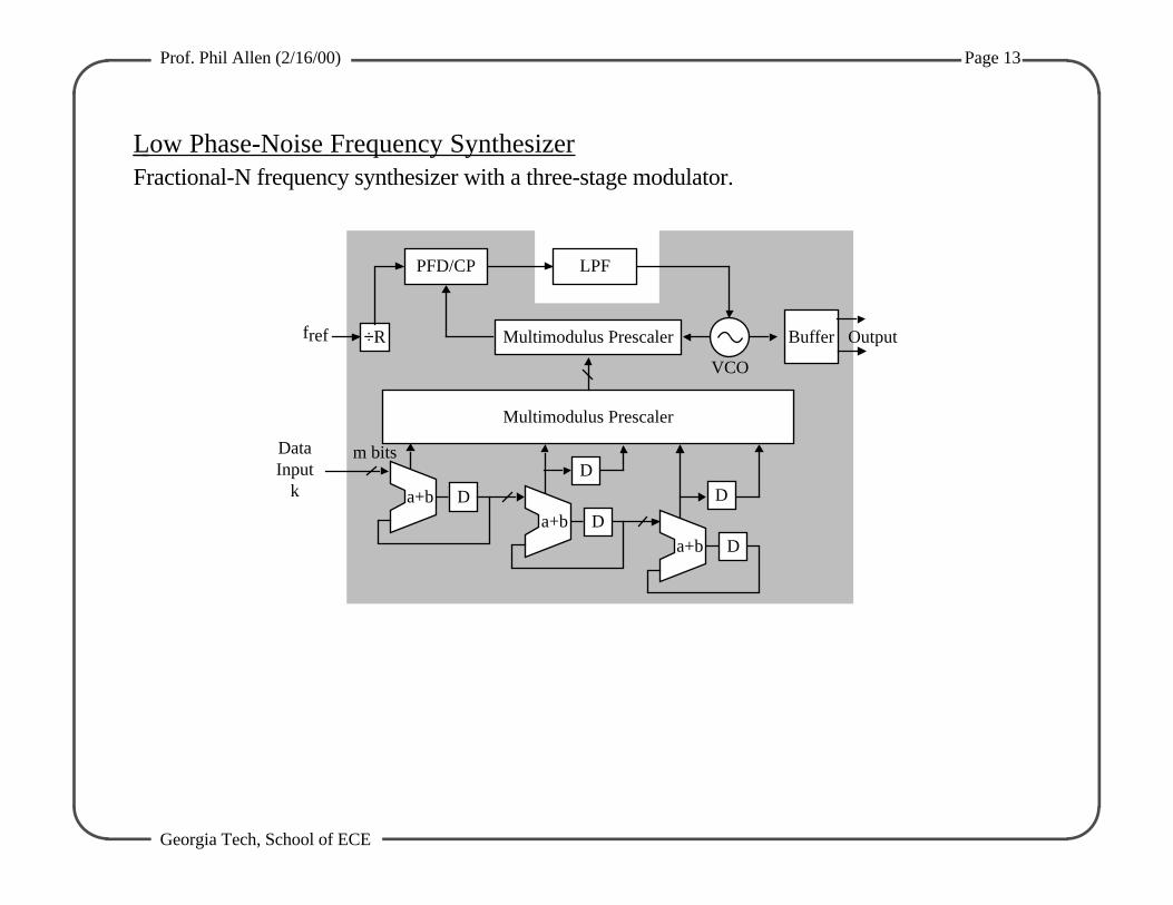
Low Phase-Noise Frequency SynthesizerFractional-N frequency synthesizer with a three-stage modulator.
Multimodulus Prescaler
Multimodulus Prescaler
Da+bDa+b
D
Da+b
D
VCO
Buffer
PFD/CP LPF
÷R Outputfref
DataInput
k
m bits
Prof. Phil Allen (2/16/00) Page 14
Georgia Tech, School of ECE
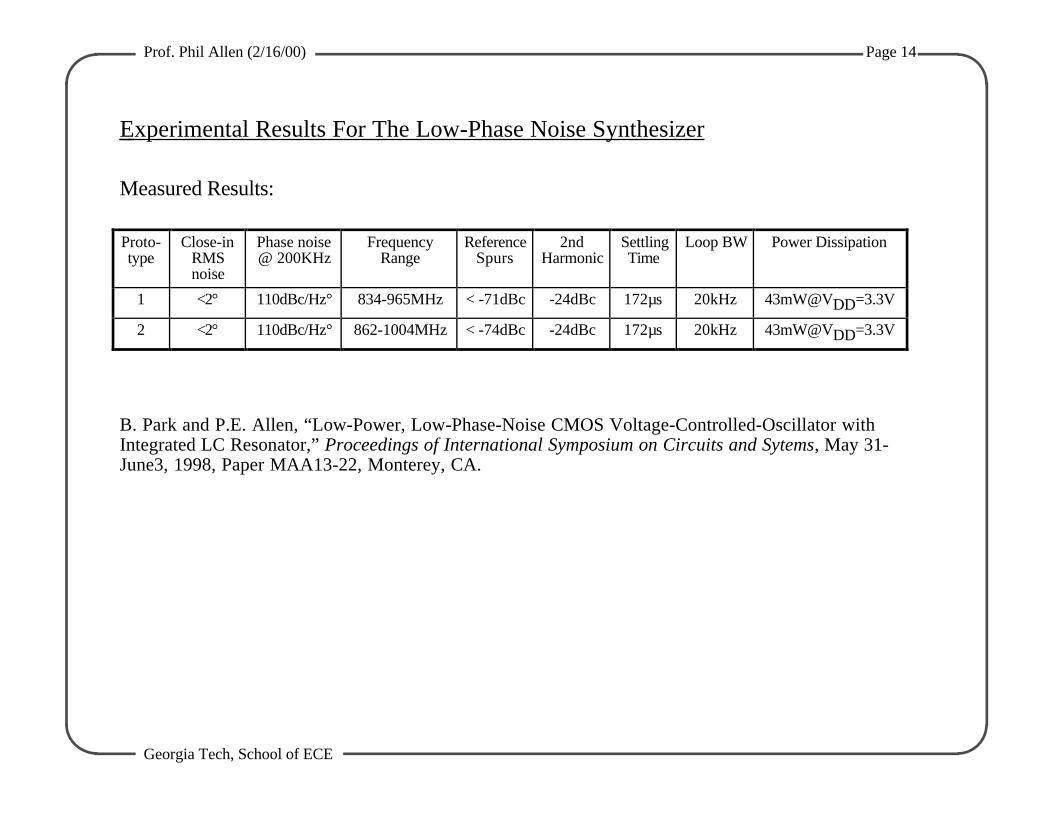
Experimental Results For The Low-Phase Noise Synthesizer
Measured Results:
Proto-type
Close-inRMSnoise
Phase noise@ 200KHz
FrequencyRange
ReferenceSpurs
2ndHarmonic
SettlingTime
Loop BW Power Dissipation
1 <2° 110dBc/Hz° 834-965MHz < -71dBc -24dBc 172µs 20kHz 43mW@VDD=3.3V
2 <2° 110dBc/Hz° 862-1004MHz < -74dBc -24dBc 172µs 20kHz 43mW@VDD=3.3V
B. Park and P.E. Allen, “Low-Power, Low-Phase-Noise CMOS Voltage-Controlled-Oscillator withIntegrated LC Resonator,” Proceedings of International Symposium on Circuits and Sytems, May 31-June3, 1998, Paper MAA13-22, Monterey, CA.
Prof. Phil Allen (2/16/00) Page 15
Georgia Tech, School of ECE
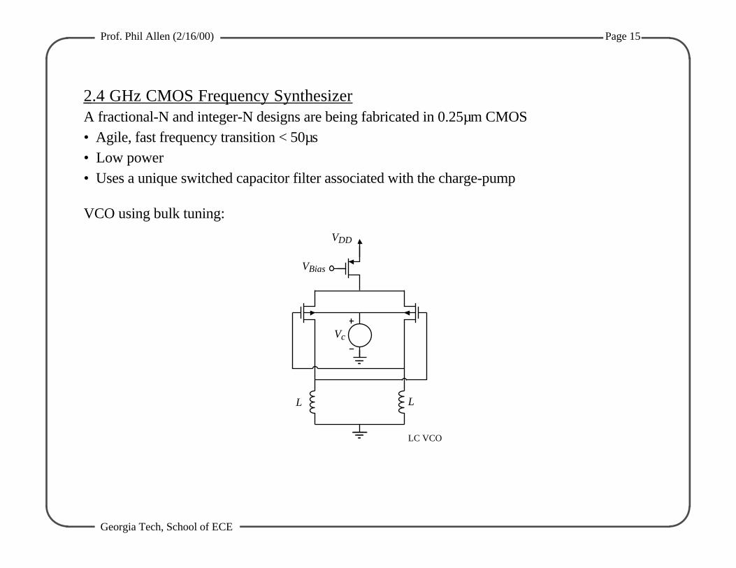
2.4 GHz CMOS Frequency SynthesizerA fractional-N and integer-N designs are being fabricated in 0.25µm CMOS• Agile, fast frequency transition < 50µs• Low power• Uses a unique switched capacitor filter associated with the charge-pump
VCO using bulk tuning:
VDD
VBias
Vc
L L
LC VCO
Prof. Phil Allen (2/16/00) Page 17
Georgia Tech, School of ECE
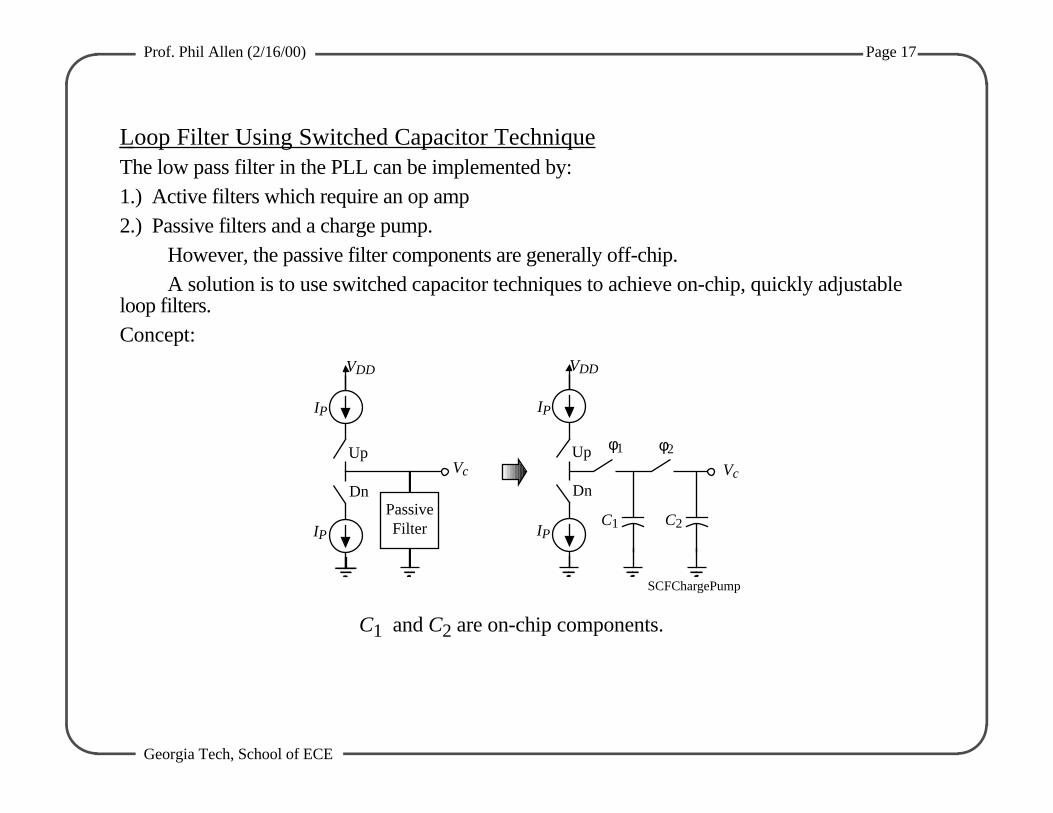
Loop Filter Using Switched Capacitor TechniqueThe low pass filter in the PLL can be implemented by:1.) Active filters which require an op amp2.) Passive filters and a charge pump.
However, the passive filter components are generally off-chip.A solution is to use switched capacitor techniques to achieve on-chip, quickly adjustable
loop filters.Concept:
PassiveFilter
Vc
VDD
IP
IP
Up
DnVc
VDD
IP
IP
Up
Dn
C1 C2
φ1 φ2
SCFChargePump
C1 and C2 are on-chip components.
Prof. Phil Allen (2/16/00) Page 24
Georgia Tech, School of ECE
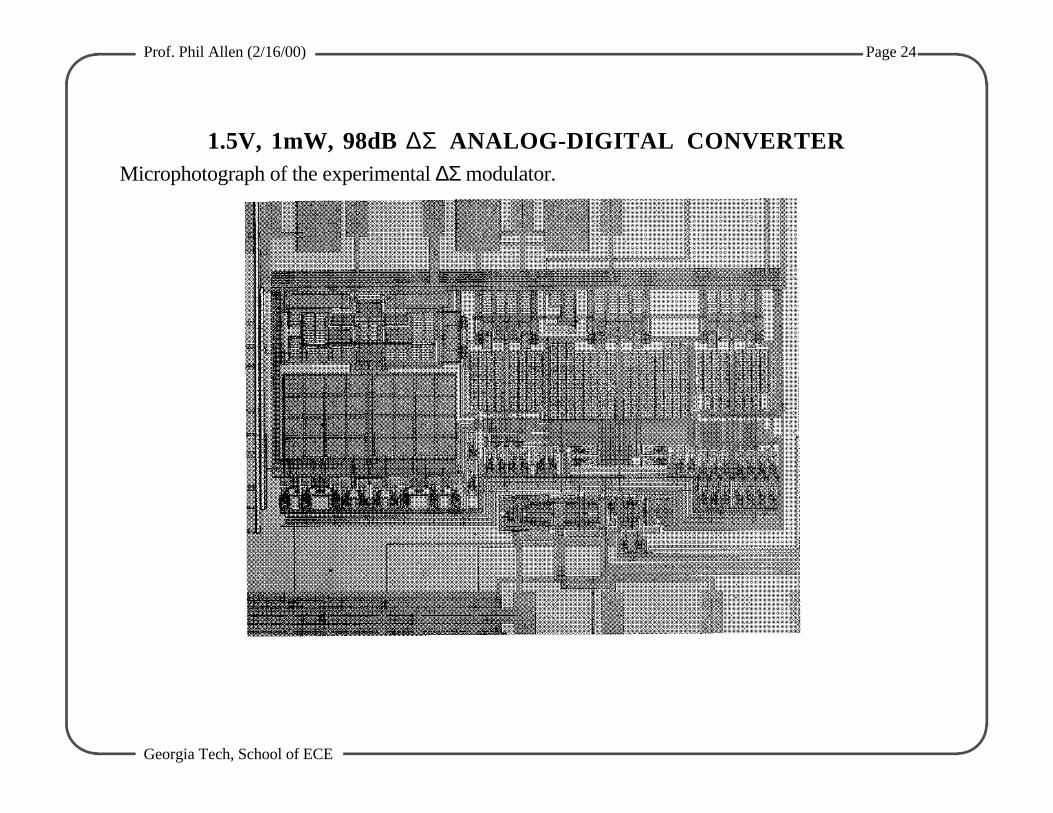
1.5V, 1mW, 98dB ∆Σ ANALOG-DIGITAL CONVERTERMicrophotograph of the experimental ∆Σ modulator.
Prof. Phil Allen (2/16/00) Page 25
Georgia Tech, School of ECE
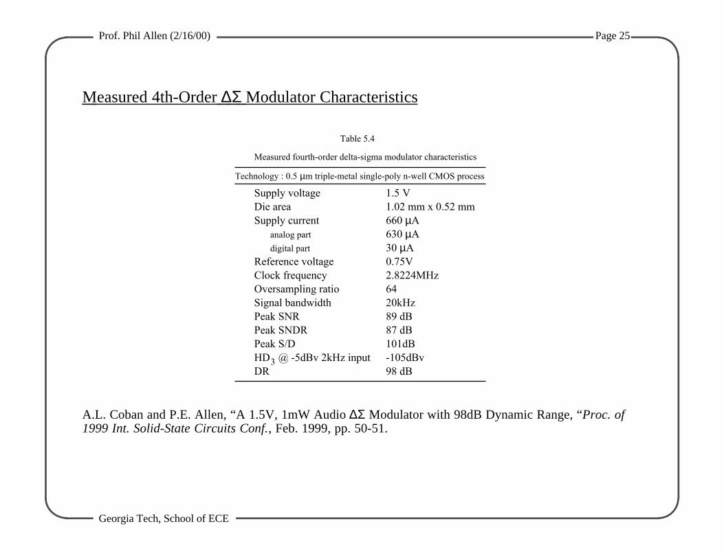
Measured 4th-Order ∆Σ Modulator Characteristics
Table 5.4
Measured fourth-order delta-sigma modulator characteristics
Technology : 0.5 µm triple-metal single-poly n-well CMOS process
Supply voltage� � 1.5 VDie area� � � 1.02 mm x 0.52 mmSupply current�� � 660 µA analog part� � � 630 µA
digital part� � 30 µAReference voltage� � 0.75VClock frequency� � 2.8224MHzOversampling ratio� � 64Signal bandwidth� � 20kHzPeak SNR� � � 89 dBPeak SNDR� � � 87 dBPeak S/D� � � 101dBHD @ -5dBv 2kHz input� -105dBvDR� � � � 98 dB
3
A.L. Coban and P.E. Allen, “A 1.5V, 1mW Audio ∆Σ Modulator with 98dB Dynamic Range, “Proc. of1999 Int. Solid-State Circuits Conf., Feb. 1999, pp. 50-51.
Prof. Phil Allen (2/16/00) Page 26
Georgia Tech, School of ECE
ON-CHIP POWER MANAGEMENTGoal: Develop an on-chip power management scheme that provides optimum power for eachblock from a single, poorly regulated (battery) with all components on chip.Requirements:• Efficient• Minimal area• Compatible with standard digital CMOS technology
Capacitors < 100pFInductors < 10nH
Approach:Power ∝ Component size x Frequency
1.) Reduce power to milliwatt level (many distributed converters)2.) Increase the switching frequency (up to 100MHz)
Prof. Phil Allen (2/16/00) Page 27
Georgia Tech, School of ECE
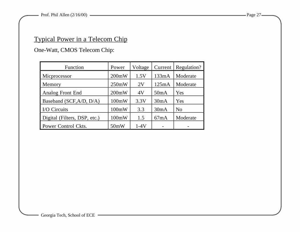
Typical Power in a Telecom Chip
One-Watt, CMOS Telecom Chip:
Function Power Voltage Current Regulation?
Micprocessor 200mW 1.5V 133mA Moderate
Memory 250mW 2V 125mA Moderate
Analog Front End 200mW 4V 50mA Yes
Baseband (SCF,A/D, D/A) 100mW 3.3V 30mA Yes
I/O Circuits 100mW 3.3 30mA No
Digital (Filters, DSP, etc.) 100mW 1.5 67mA Moderate
Power Control Ckts. 50mW 1-4V - -
Prof. Phil Allen (2/16/00) Page 28
Georgia Tech, School of ECE
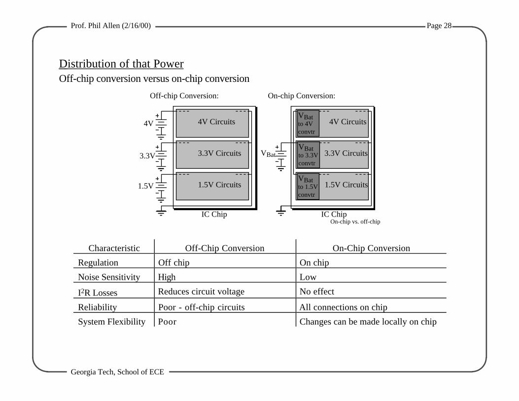
Distribution of that PowerOff-chip conversion versus on-chip conversion
4V
3.3V
1.5V
4V Circuits
3.3V Circuits
1.5V Circuits
IC Chip
Off-chip Conversion:
4V Circuits
3.3V Circuits
1.5V Circuits
IC Chip
On-chip Conversion:
VBatto 3.3Vconvtr
VBatto 4Vconvtr
VBatto 1.5Vconvtr
VBat
On-chip vs. off-chip
Characteristic Off-Chip Conversion On-Chip Conversion
Regulation Off chip On chip
Noise Sensitivity High Low
I2R Losses Reduces circuit voltage No effect
Reliability Poor - off-chip circuits All connections on chip
System Flexibility Poor Changes can be made locally on chip
Prof. Phil Allen (2/16/00) Page 29
Georgia Tech, School of ECE
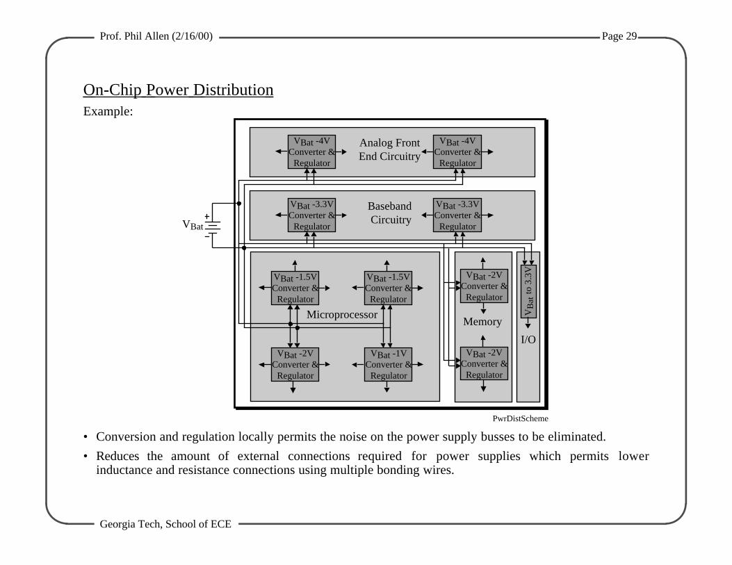
On-Chip Power Distribution Example:
VBat -4VConverter &
Regulator
VBat -4VConverter &
Regulator
Analog FrontEnd Circuitry
VBat
VBat -1.5VConverter &
Regulator
VBat -3.3VConverter &
Regulator
VBat -3.3VConverter &
Regulator
Baseband Circuitry
VBat -1.5VConverter &
Regulator
Microprocessor
VBat -2VConverter &
Regulator
VBat -1VConverter &
Regulator
VBat -2VConverter &
Regulator
VBat -2VConverter &
Regulator
Memory
I/O
VB
at to
3.3
V
PwrDistScheme
• Conversion and regulation locally permits the noise on the power supply busses to be eliminated.
• Reduces the amount of external connections required for power supplies which permits lowerinductance and resistance connections using multiple bonding wires.
Prof. Phil Allen (2/16/00) Page 30
Georgia Tech, School of ECE
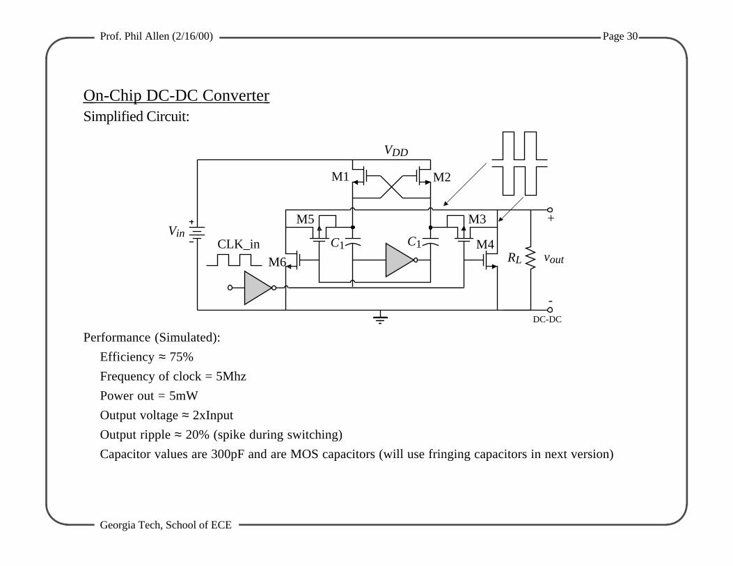
On-Chip DC-DC Converter Simplified Circuit:
VDD
C1
M1
CLK_in
M2
M3
M4
DC-DC
M5
M6
C1voutRL
Vin+
-
Performance (Simulated):
Efficiency ≈ 75%
Frequency of clock = 5Mhz
Power out = 5mW
Output voltage ≈ 2xInput
Output ripple ≈ 20% (spike during switching)
Capacitor values are 300pF and are MOS capacitors (will use fringing capacitors in next version)
Prof. Phil Allen (2/16/00) Page 31
Georgia Tech, School of ECE
RECENT PUBLICATIONS
1. G.A. Rincon-Mora and P.E. Allen, "A Low-Voltage, Low Quiescent Current, Low Drop-OutRegulator," J. of Solid-State Circuits, Vol. 33, No. 1, January 1998, pp. 36-44.2. G.A. Rincon-Mora and P.E. Allen, “Optimized Frequency-Shaping Circuit Topologies forLDO’s,” Trans. on Circuits and Systems-II, Vol. 45, No. 6, June 1998, pp. 703-708.3. B.J. Blalock, P.E. Allen, and G.A Rincon-Mora, “Designing 1-V Op Amps Using StandardDigital CMOS Technology,” Trans. on Circuits and Systems-II, vol. 45, no. 7, July 1998, pp.769-780.4. G.A. Rincon-Mora and P.E. Allen, “A 1.1-V Current-Mode and Piecewise-Linear Curvature-Corrected Bandgap Reference,” J. of Solid-State Circuits, vol. 33, no. 10, October 1998, pp.1551-1554.5. B. Park and P.E. Allen, "1 GHz, low-phase noise CMOS frequency synthesizer withintegrated LC VCO for wireless communications," Proceedings of CICC, May 1998, pp. 567-570.6. A.L. Coban and P.E. Allen, “A 1.5V, 1mW Audio ∆Σ Modulator with 98dB Dynamic Range,Proc. of 1999 Int. Solid-State Circuit Conf., Feb. 1999, pp. 50-51.7. G.K. Balachandran and P.E. Allen, “A Low-Voltage, Fully-Differential, Switched-CurrentMemory Cell”, Electronic Letters, Vol. 35, No. 25, Dec. 1999, pp. 2200-2201.
Prof. Phil Allen (2/16/00) Page 32
Georgia Tech, School of ECE
SUMMARY
• EDAConverting from quarter to semester systemNew faculty member - Prof. Steve Kenney, ON Semiconductor Jr. ProfessorLooking for two more faculty members in analog area
• 13 Ph.D students and 2 MS students• Program focus is on wireless applications suitable for wide range applications• Emphasis of the research is:
On-chip RF, IF, and baseband filtersHigh performance frequency synthesizers
• Working closely with Prof. Joy Laskar to develop system solutions to:Bluetooth 28 dBm specification in CMOS technologyIEEE 802 WLAN specifications in SiGe technology


![Ece-III-Analog Electronic Ckts [10es32]-Notes](https://img.pdfslide.us/doc/110x75/55cf9da2550346d033ae7b1a/ece-iii-analog-electronic-ckts-10es32-notes.jpg)