Embed Size (px)
Citation preview

Aryanto et al. Journal of Theoretical and Applied Physics 2013, 7:27http://www.jtaphys.com/content/7/1/27
RESEARCH Open Access
The impact of AsH3 overflow time and indiumcomposition on the formation of self-assembledInxGa1 − xAs quantum dots studied by atomicforce microscopyDidik Aryanto1,2*, Zulkafli Othaman2 and Abd Khamim Ismail2
Abstract
We have performed atomic force microscopy to investigate the effect of various indium compositions andvarious AsH3 flow times during cooling on the formation of self-assembled InxGa1 − xAs quantum dots (QDs).The InxGa1 − xAs QDs were grown by metal-organic chemical vapour deposition using the Stranski-Krastanow (S-K)growth mode. The migration of group III species in the growth of InxGa1 − xAs QDs is influenced by the AsH3 flowduring the cooling period due to the increasing surface population of the active arsenic species. It influences thesize and density of the dots on the surface. For various indium compositions, an increase in InxGa1 − xAs QD densitywith increasing indium composition is observed. It indicates that the dot density depends on lattice parameters.The dot density is inversely proportional to surface diffusion (ρ ∝ R/D), with D = (2kT/h)/a2 exp(−ED/kT). In thegrowth of InxGa1 − xAs QDs using the S-K growth mode, the dots were formed on the surface as the effect ofelastic strain relaxation due to the lattice mismatch. Increasing indium composition affects the lattice mismatch ofthe InxGa1 − xAs/GaAs QD system, which influences the dot formation on the surface. However, due to thestochastic nature of the nucleation of self-assembled growth, control of the spatial ordering of the QDs has provedto be extremely challenging.
Keywords: Quantum dots, Atomic force microscopy, Lattice mismatch, Surface diffusion
IntroductionThe fabrication of quantum dots (QDs) by self-assembledprocesses has attracted increasing attention in the last fewyears. This is of great importance for fundamental studiesas well as applications in novel semiconductor devices.The QDs show unique physical properties due to theirzero-dimensional density of states [1,2] which can be usedfor the realization of quantum dot lasers with very lowthreshold current density and very high characteristictemperature [3-6]. Self-assembled InxGa1 − xAs QD struc-tures have been considered as one of the promising candi-dates for 1.3-μm-long-wavelength devices [7]. It is a
* Correspondence: [email protected] Department, Faculty of Mathematics and Science Education, InstitutKeguruan dan Ilmu Pendidikan PGRI Semarang, Semarang 50125, Indonesia2Quantum Structure Research Group, Ibnu Sina Institute for FundamentalScience Studies, Universiti Teknologi Malaysia, Skudai, Johor Bahru 81310,Malaysia
© 2013 Aryanto et al.; licensee Springer. This isAttribution License (http://creativecommons.orin any medium, provided the original work is p
promising material for attractive optical device applica-tions, such as QD lasers [8,9] and QD infrared photode-tectors [10,11]. The performance of quantum dot devicesis affected by the size, shape, uniformity, composition,density and structure of the dots [12].High-quality InxGa1 − xAs QDs can be easily fabricated
by MBE or metal-organic chemical vapour deposition(MOCVD) via a self-assembled process known as theStranski-Krastanow (S-K) growth mode [13]. The growthof InxGa1 − xAs QDs on a GaAs substrate using the S-Kmode is based on the lattice mismatch at the interface be-tween 0% and7.2%, which causes lattice strain in the layerand creates defects, especially misfit dislocations at theinterface. The quality of InxGa1 − xAs QDs grown onlattice-mismatched GaAs depends largely on the indiumcomposition (x) and the thickness of the epilayer [14]. Ifthe lattice mismatch between the QDs and substrate issmall and the layer is thin, the mismatch is accommodated
an Open Access article distributed under the terms of the Creative Commonsg/licenses/by/2.0), which permits unrestricted use, distribution, and reproductionroperly cited.

Aryanto et al. Journal of Theoretical and Applied Physics 2013, 7:27 Page 2 of 6http://www.jtaphys.com/content/7/1/27
by strain in the layer [15]. In the S-K growth mode, themismatched epitaxy is initially accommodated by biaxialcompression in a layer-by-layer (two-dimensional (2D))growth region, traditionally called the wetting layer. Afterthe deposition of a few monolayers, the strain energy in-creases and the development of islands (three-dimensional(3D)) becomes more favourable than the planar growth[16]. There are some problems, however, such as the inev-itable two-dimensional wetting layer residue, poor sizecontrollability, no ordering and very narrow range ofgrowth conditions. A number of studies have shown thatthe growth of QDs by the S-K growth mode is complexand very sensitive to growth conditions such as growthtemperature [1], growth rate [17] and V/III ratio [5,18].There are not many publications on the effects of indiumcomposition and AsH3 flow time during the coolingperiod on the QD formations. In this work, we report thesurface morphology studies of InxGa1 − xAs QDs byatomic force microscopy (AFM) measurement as the im-pacts of various AsH3 flow periods during cooling and in-dium composition in the QD formation.
ExperimentSelf-assembled InxGa1 − xAs QDs were grown on GaAs(100) substrates via the S-K growth mode by MOCVD.Precursors used for the growth of the GaAs layer andInxGa1 − xAs QDs were trimethylgallium (TMGa),trimethylindium (TMIn) and arsine (AsH3). The groupIII source materials were TMGa and TMIn, held intemperature-controlled baths at −3.5°C and 17°C, re-spectively, while arsine diluted to 10% in hydrogen wasthe group V source. Palladium-diffused hydrogen wasused as the carrier gas. Prior to the growth, the substratetemperature was increased up to 700°C for 10 min underarsine flow to remove oxides on the substrate surface. Thegrowth was initiated from the GaAs buffer layer with athickness of 200 nm at 650°C, and then temperaturewas reduced to 550°C for the growth of self-assembledInxGa1 − xAs QDs. Three samples with deposition timesof 4.5, 5 and 6 s were prepared. Other samples with 3and 1 min of AsH3 overflow during cooling down afterInxGa1 − xAs deposition were also prepared. Thenominal indium composition of the self-assembledInxGa1 − xAs QDs was varied between 40% and 70%with a V/III ratio fixed at 10.1 during deposition. Thegrowth rate for InxGa1 − xAs QDs was set at 1.1 μm/h,and the total pressure of the reactor was kept at 76 Torrduring the growth. The surface morphologies of all thesamples were studied in air at room temperature usinga SII AFM system. AFM is ideally suited for both thevisualization of nanostructure materials and the meas-urement of the spatial dimensions of features on thenanomaterial surfaces.
Results and discussionFigure 1 shows AFM micrographs of InxGa1 − xAs QDson GaAs (100) substrates with growth times of 4.5, 5and 6 s. These AFM images show the change of the sur-face morphology of InxGa1 − xAs QDs with increasinggrowth time. The area density of InxGa1 − xAs QDs forsamples (a), (b) and (c) is 1.04 × 10¹⁰, 1.59 × 10¹⁰ and1.14 × 1010 cm−2, respectively. A high dot density in theorder of 1010 cm−2 for all samples is in agreement withother studies [6,7,12] on InxGa1 − xAs QDs. AFManalysis also shows that the average height and diameterof InxGa1 − xAs QDs for samples (a), (b), and (c) are7 nm × 18 nm, 9 nm × 24 nm and 13 nm × 35 nm,respectively. An increase in the QD size and someexcessive large dots (coalesced dots) were observed inthe case of 5 and 6 s of growth time. The size of theInxGa1 − xAs QDs gradually increases and the dot dens-ity decreases with increasing growth time of QDs. Thelarge dots formed mainly due to the coalescence of smalldots. Evidence for the occurrence of this coalescence canbe detected from the increase in the number of relativelylarger dots with decreasing density. Although the mech-anism of large dot formation is not yet well understood,they probably form due to the large migration distanceof indium atoms along the GaAs step edges [12]. An in-crease in both diameter and height was observed withincreasing growth time. This is due to the increase inthe dot nuclei on the surface because the longer growthtime of QDs causes the migration of indium and galliumatoms.Another reason for the larger dots to form on the sur-
face was because the deposition layer during the S-Kgrowth mode was thicker than the critical thickness.The coherent dots appear beyond a critical thickness ofthe deposited layer during the S-K growth mode. In-creasing growth time contributed to the exceedance ofthe self-assembled QD thickness beyond the criticalthickness, which then contributed to the formation ofseveral large dots as shown in AFM images. The S-Kgrowth mode is a damage-free formation of dot struc-tures directly on the epilayer surface by self-assembledmechanisms. However, the QDs are not sufficiently uni-form in size and distribution [12].Figure 2 shows typical AFM images of InxGa1 − xAs
QDs grown on GaAs substrates with (a) 3 and (b) 1 minof AsH3 overflow period during cooling down. TheseAFM images show that the dots are elongated in the 1�10½ �direction with different AsH3 overflow periods. It was be-cause the dots were easily grown near the step edges ofGaAs multi-atomic steps compared to the terrace centres.In the deposition process during epitaxial growth byMOCVD, the GaAs multi-atomic steps naturally formedalong the 1�10½ � direction as an effect of substratemisorientation. The morphology of the GaAs buffer layer

Figure 1 AFM images of InxGa1 − xAs QDs with (a) 4.5, (b) 5 and (c) 6 s of growth time.
Aryanto et al. Journal of Theoretical and Applied Physics 2013, 7:27 Page 3 of 6http://www.jtaphys.com/content/7/1/27
strongly influences the dot formation on the surface asshown by Xie et al. [19]. The AFM measurements showthat the average dot height was 7 nm, the average diam-eter was 18 nm and the density was 1.04 × 1010 cm−2 with3 min of AsH3 overflow period, while the InxGa1 − xAsQDs on the GaAs substrate with 1 min of AsH3 overflowduring cooling have an average diameter of 23 nm, heightof 8 nm and density of 4.54 × 1010 cm−2.The AsH3 overflow time during cooling strongly af-
fects dot nucleation. The dot density and morphologydrastically change with different periods of AsH3 over-flow during this cooling down. The longer AsH3 over-flow period causes quicker nucleation of InxGa1 − xAsQDs, which then results in larger size and low QD dens-ity. The different AsH3 overflow periods during coolingaffect the migration of gallium and indium atoms due tothe increase of the surface population of active AsH3
species. Riel et al. [20] stated that the migration of groupIII species is due to the AsH3 pressure. However, theexact mechanism by which AsH3 encourages indiumand gallium redistribution is still unclear. The AsH3
overflow during cooling may affect the kinetics of thedot formation by changing its binding energy. Thesethen change the surface energy and thermodynamicequilibrium of the QD ensembles. In principle, both
Figure 2 AFM images of InxGa1 − xAs QDs grown on GaAs substrates
kinetic and thermodynamic limitations can influence thesize, shape, uniformity, density and composition of thedots.Figure 3a,b,c,d compares the surface morphology of
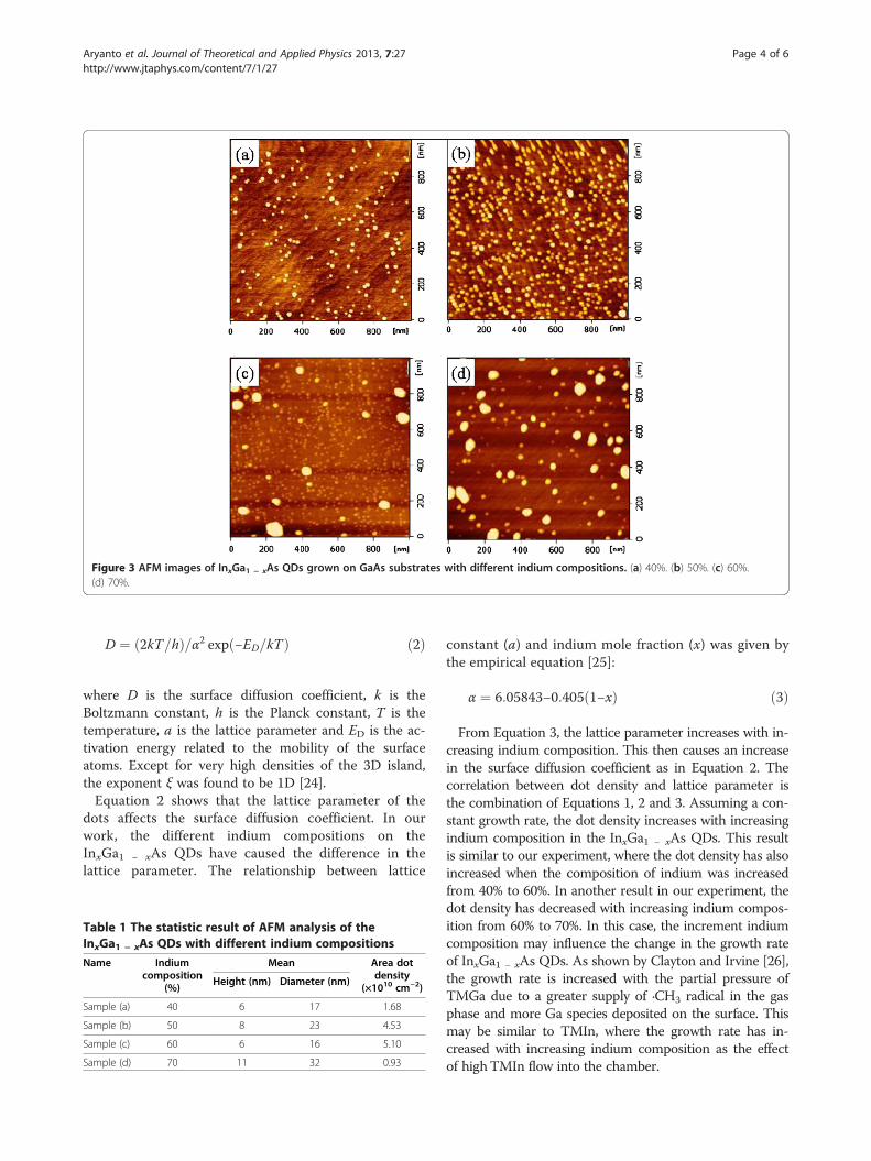
the InxGa1 − xAs QDs deposited with different indiumcompositions. The statistical result of the former sam-ples by AFM analysis is shown in Table 1. When the in-dium composition is increased from 40% to 70%, theaverage dot size and density fluctuate. The main reasonfor the evolution of the dots on the growth of self-assembled InxGa1 − xAs QDs is the different criticalthicknesses of the dots due to the increment of indiumcomposition. In the S-K growth mode, when the thick-ness of the dots is more than the critical layer thickness,several small dots are merged into larger dots which de-creases the area dot density [21,22].In general, sizes and densities show an inverse behav-
iour: with increasing deposition temperature and de-creasing deposition rate, R, the typical sizes of thecoherent dots increase, whereas the typical surface dens-ities decrease [23]. The mathematical calculation of thedensity (ρ) follows power nucleation:
ρ∝ R=Dð Þξ ð1Þ
with different AsH3 overflow periods. (a) 3 min. (b) 1 min.
2
Figure 3 AFM images of InxGa1 − xAs QDs grown on GaAs substrates with different indium compositions. (a) 40%. (b) 50%. (c) 60%.(d) 70%.
Aryanto et al. Journal of Theoretical and Applied Physics 2013, 7:27 Page 4 of 6http://www.jtaphys.com/content/7/1/27
D ¼ 2kT=hð Þ=α exp −ED=kTð Þ ð2Þ
where D is the surface diffusion coefficient, k is theBoltzmann constant, h is the Planck constant, T is thetemperature, a is the lattice parameter and ED is the ac-tivation energy related to the mobility of the surfaceatoms. Except for very high densities of the 3D island,the exponent ξ was found to be 1D [24].Equation 2 shows that the lattice parameter of the
dots affects the surface diffusion coefficient. In ourwork, the different indium compositions on theInxGa1 − xAs QDs have caused the difference in thelattice parameter. The relationship between lattice
Table 1 The statistic result of AFM analysis of theInxGa1 − xAs QDs with different indium compositionsName Indium
composition(%)
Mean Area dotdensity
(×1010 cm−2)Height (nm) Diameter (nm)
Sample (a) 40 6 17 1.68
Sample (b) 50 8 23 4.53
Sample (c) 60 6 16 5.10
Sample (d) 70 11 32 0.93
constant (a) and indium mole fraction (x) was given bythe empirical equation [25]:
α ¼ 6:05843−0:405 1−xð Þ ð3Þ
From Equation 3, the lattice parameter increases with in-creasing indium composition. This then causes an increasein the surface diffusion coefficient as in Equation 2. Thecorrelation between dot density and lattice parameter isthe combination of Equations 1, 2 and 3. Assuming a con-stant growth rate, the dot density increases with increasingindium composition in the InxGa1 − xAs QDs. This resultis similar to our experiment, where the dot density has alsoincreased when the composition of indium was increasedfrom 40% to 60%. In another result in our experiment, thedot density has decreased with increasing indium compos-ition from 60% to 70%. In this case, the increment indiumcomposition may influence the change in the growth rateof InxGa1 − xAs QDs. As shown by Clayton and Irvine [26],the growth rate is increased with the partial pressure ofTMGa due to a greater supply of ·CH3 radical in the gasphase and more Ga species deposited on the surface. Thismay be similar to TMIn, where the growth rate has in-creased with increasing indium composition as the effectof highTMIn flow into the chamber.

Aryanto et al. Journal of Theoretical and Applied Physics 2013, 7:27 Page 5 of 6http://www.jtaphys.com/content/7/1/27
Yu et al. [6] showed that a higher indium component re-duces the critical thickness as observed in this work at70% indium composition. The increasing indium atomstend to adhere to the existing QDs when growth interrup-tion was introduced in the QD-forming period andresulting larger dots. On the other hand, the dot densityincreases as the indium composition increases. The pre-existing indium atoms play the role of nucleation sites andthe origin of the shortened diffusion length [27]. In thiswork, the increment of indium composition contributedto the increase of dot density, but at a higher indium com-position (0.7), the dots became larger in size and have de-creased in area density as shown in the AFM images.In the formation of self-assembled InxGa1 − xAs QDs
via the S-K growth mode, the dot formation (3D) occursfollowing the layer-by-layer/wetting layer (2D). The tran-sition from layer-by-layer to dot growth occurs at thecritical layer thickness which is slightly dependent onthe surface energy, strain energy and lattice mismatch ofthe system [6,28]. When InxGa1 − xAs is deposited onthe GaAs substrate, the possibility of the island forma-tion process on the surface can be understood with theequilibrium growth mode or interfacial misfit disloca-tion. Since the formation of the wetting layer (2D) oc-curs on the surface, as the wetting layer gets thicker, theassociated strain energy increases rapidly. In order to re-lieve the strain, the island occurs in either a dislocatedor an elastic deformation [29].In dislocated islands, strain relief arises by forming inter-
facial misfit dislocation. The reduction of strain energy isaccommodated by the introduction of generally greaterthan the concomitant cost of increased surface energy as-sociated with creating the cluster. The dot formation de-pends on the critical thickness of the wetting layer, whichis strongly dependent on the lattice mismatch betweenInxGa1 − xAs QDs and GaAs substrate. In another case,the dislocation-free dots can be formed during the S-Kgrowth mode by the introduction of undulation into thenear-surface layer of the substrate. These regions of localcurvature serve to elastically deform both the substrateand dots. Because of this, the S-K growth mode is typicallysynonymous with the growth of a wetting layer followedby the nucleation of elastically strained islands, rather thanislands containing dislocations [29]. The dots were formedon the surface as the effect of the elastic strain relaxationof the lattice mismatch.The mismatch between the lattices causes a strain
known as the lattice mismatch strain, which can be de-fined as:
f ≡αs−αeαe
ð4Þ
where as is the relaxed lattice constant of the substrateand ae is the relaxed lattice constant of the epitaxial layer.
The variation of indium composition affects the latticemismatch of the InxGa1 − xAs/GaAs QD system. The lat-tice mismatch increases with increasing indium compos-ition in the dots (Equation 4). The QD formation,evolution and defect introduction depend strongly on thebalance between the surface energy and the strain energyof the system and the growth kinetics. In the growth ofself-assembled hetero-epitaxial QDs, the effect of straindue to the lattice mismatch between the substrate andepilayer is an important factor on the surface morphology.
ConclusionThe surface properties of self-assembled InxGa1 − xAsQDs grown on GaAs substrates using the S-K growthmode have been analyzed by AFM. Different AsH3 over-flow times during cooling down period and indium com-positions on the self-assembled InxGa1 − xAs QDs haveaffected the dot formation on the surface. The AsH3
overflow during cooling affects the change in the surfaceenergy and thermodynamic equilibrium of the QD en-sembles. For the various indium compositions investi-gated, the density of the dots was strongly influenced bythe lattice parameter. The surface diffusion of the dotschanges with the change in the lattice parameter as theeffect of different indium compositions in the self-assembled InxGa1 − xAs QDs. The formation of the dotsvia the S-K growth mode is slightly dependent on thelattice mismatch system. The variation of indium com-position affects the lattice mismatch of InxGa1 − xAsQDs, which then causes the change in the area dot dens-ity. Various indium compositions on the growth of QDshave also shown the effect of surface diffusion and latticemismatch on dot formation.
Competing interestsThe authors declare that they have no competing interests.
Authors’ contributionsDA, ZO and AKI conceived of the study and participated in its design andcoordination. All authors read and approved the final manuscript.
AcknowledgementsThis work was supported by the Ministry of Science, Technology andInnovation, Malaysia. The authors are also grateful to Ibnu Sina Institute forFundamental Science Studies, Universiti Teknologi Malaysia for providing thelaboratory facilities.
Received: 27 September 2012 Accepted: 24 May 2013Published: 4 June 2013
References1. Heinrichsdorff, F, Korst, A, Grundmann, M, Bimberg, D, Bertram, F, Christen, J,
Kogosov, A, Werner, P: Self organization phenomena of InGaAs/GaAsquantum dots grown by metalorganic chemical vapor deposition. J. CrystalGrowth 170, 568–573 (1997)
2. Bimberg, D, Grundmann, M, Ledentsov, NN: Quantum Dot Heterostructures.Wiley, Chichester (1999)
3. Bimberg, D, Grundmann, M, Heinrichsdorff, F, Ledentsov, NN, Ustinov, VM,Zhukov, AE, Kovsh, AR, Maximov, MV, Shernyakov, YM, Volovik, BV,Tsatsulnikov, AF, Kopev, PS, Alferov, ZI: Quantum dot lasers: breakthrough inoptoelectronics. Thin Solid Films 367, 235–249 (2000)

Aryanto et al. Journal of Theoretical and Applied Physics 2013, 7:27 Page 6 of 6http://www.jtaphys.com/content/7/1/27
4. Maximov, MV, Ledentsov, NN, Ustinov, VM, Alferov, ZI, Bimberg, D: GaAs-based 1.3 μm InGaAs quantum dot lasers: a status report. J. ElectronicMaterials 29(5), 476–486 (2000)
5. Kim, JS, Oh, DK, Yu, PW, Leem, JY, Lee, JI, Lee, CR: Optical characteristics ofself-assembled InAs quantum dots with InGaAs grown by a molecular beamepitaxy. J. Crystal Growth 261, 38–43 (2004)
6. Yu, LK, Xu, B, Wang, ZG, Jin, P, Zhao, C, Lei, W, Sun, J, Li, K, Hu, LJ, Liang, LY:The effect of In content on high-density InxGa1-xAs quantum dots. J. CrystalGrowth 282, 173–178 (2005)
7. Lan, Q, Niu, ZC, Zhou, DY, Kong, YC, Wang, XD, Miao, ZH, Feng, SL: Surfacemorphology and optical property of 1.3 μm In0.5Ga1-xAs/GaAs self-organizedquantum dots grown by MBE. Physica E 17, 114–116 (2003)
8. Germann, TD, Strittmatter, A, Kettler, T, Posilovic, K, Pohl, UW, Bimberg, D:MOCVD of InGaAs/GaAs quantum dots for laser emitting close to 1.3 μm.J Crystal Growth 298, 591–594 (2007)
9. Grundmann, M, Ledentsov, NN, Hopfer, F, Heinrichsdorff, F, Guffarth, F,Bimberg, D, Ustinov, VM, Zhukov, AE, Kovsh, AR, Maximov, MV, Musikhin, YG,Alferov, ZHI, Lott, JA, Zhakharov, ND, Werner, P: Long-wavelength quantum-dots lasers. J. Material Science in Electronics 13, 643–647 (2002)
10. Lim, JY, Nam, HD, Song, JD, Choi, WJ, Lee, JI, Yang, HS: Characterization ofIn0.5Ga0.5As quantum dot infrared photodetector (QDIP) structures treatedwith post-growth processes. Curr. Appl. Phys. 6S1, e33–e37 (2006)
11. Jiang, L, Li, SS, Liu, W-S, Yeh, N-T, Chyi, J-I: A two-stack, multi-colorIn0.5Ga0.5As/GaAs and InAs/GaAs quantum dot infrared photodetector forlong wavelength infrared detection. Infrared Physics & Technology46, 249–256 (2005)
12. Ishihara, T, Lee, S, Akabori, M, Motohisa, J, Fukui, T: Dependence on Incontent of InGaAs quantum dots grown along GaAs multiatomic steps byMOVPE. J. Crystal Growth 237–239, 1476–1480 (2002)
13. Ng, J, Missous, M: Improvement of stacked self-assembled InAs/GaAsquantum dots structures for 1.3 μm applications. Microelectron.J 37, 1446–1450 (2006)
14. Dyk, EEV, Leitch, AWR, Neethling, JH: High quality InxGa1-xAs epitaxial layersgrown on GaAs by MOVPE. J. Phys. Stat. Sol. (a) 189, 223–231 (2002)
15. Jasik, A, Kosiel, K, Strupiński, W, Wesołowski, M: Influence of covering oncritical thickness of strained InxGa1-xAs layer. Thin Solid Films 412, 50–54(2002)
16. Henini, M: Properties and applications of quantum dots heterostructuresgrown by molecular beam epitaxy. Nanoscale Res. Lett. 1, 32–45 (2006)
17. Joyce, PB, Krzyzewski, TJ, Bell, GR, Jones, TS, Malik, S, Childs, D, Murray,R: Growth rate effects on the size, composition and optical properties ofInAs/GaAs quantum dots grown by molecular beam epitaxy. J. CrystalGrowth 227–228, 1000–1004 (2001)
18. Jiang, L, Lin, T, Wei, X, Wang, GH, Zhang, GZ, Zhang, HB, Ma, XY: Effect of V/III ratio on InGaAs and InP grown at low temperature by LP-MOCVD. J.Crystal Growth 260, 23–27 (2004)
19. Xie, Q, Brown, JL, Jones, RL, Nostrand, JEN: Shape stabilization and sizeequalization of InGaAs self organized quantum dots. J. Electronic Materials28(12), L24–L45 (1999)
20. Riel, BJ, Hinzer, K, Moisa, S, Fraser, J, Finnie, P, Piercy, P, Fafard, S, Wasilewski,Z: InAs/GaAs(100) self-assembled quantum dots, arsenic pressure andcapping effects. J. Crystal Growth 236, 145–154 (2002)
21. Song, JD, Choi, WJ, Lee, JI, Lee, JY: Structural and optical properties ofIn0.5Ga0.5As/GaAs quantum dots in an In0.1Ga0.9As well using repeatdepositions of InAs/GaAs short-period superlattices for the application ofoptical communication. Physica E 32, 115–118 (2006)
22. Kim, JS, Kim, JS: Formation of InAs/GaAs quantum dots by alternatinggrowth of InAs and GaAs with a quasi monolayer thickness. J. KoreanPhysical Society 49(1), 195–198 (2006)
23. Johanson, J, Carlson, N, Seifert, W: Manipulations of size and density of self-assembled quantum dots grown by MOVPE. Physica E 2, 667–671 (1998)
24. Seifert, W, Johansson, J, Carlsson, N, Gustafsson, A, Malm, J-O: Continuousand discontinuous metal-organic vapour phase epitaxy of coherent self-assembled islands: effects on size homogeneity. J. Crystal Growth197, 19–24 (1999)
25. Pal, R, Singh, M, Murlidharan, R, Agarwal, SK, Pal, D, Bose, DN: Latticemismatch and surface morphology studies of InxGa1-xAs epilayers grown onGaAs substrates. J. Bulk. Mater. Sci. 21, 313–316 (1998)
26. Clayton, AJ, Irvine, SJC: The kinetics of parasitic growth in GaAs MOVPE. J.Crystal Growth 300, 277–283 (2007)
27. Park, SK, Tatebayashi, J, Yang, T, Kim, JS, Kim, EK, Arakawa, Y: InAs/AlAsquantum dots with InGaAs insertion layer, dependence of the indiumcomposition and the thickness. Physica E 26, 138–142 (2005)
28. Henini, M, Patanè, A, Polimeni, A, Levin, A, Eaves, L, Main, PC, Hill, G:Electrical and optical properties of self-assembled quantum dots.Microelectron J. 33, 313–318 (2002)
29. Woll, AR, Rugheimer, P, Lagally, MG: Self-organized quantum dots. In:Borosvitskaya, E, Shur, MS (eds.) Quantum Dots, pp. 45–78. World Scientific,Singapore (2002)
doi:10.1186/2251-7235-7-27Cite this article as: Aryanto et al.: The impact of AsH3 overflow time andindium composition on the formation of self-assembled InxGa1 − xAsquantum dots studied by atomic force microscopy. Journal of Theoreticaland Applied Physics 2013 7:27.
Submit your manuscript to a journal and benefi t from:
7 Convenient online submission
7 Rigorous peer review
7 Immediate publication on acceptance
7 Open access: articles freely available online
7 High visibility within the fi eld
7 Retaining the copyright to your article
Submit your next manuscript at 7 springeropen.com