Embed Size (px)
Citation preview
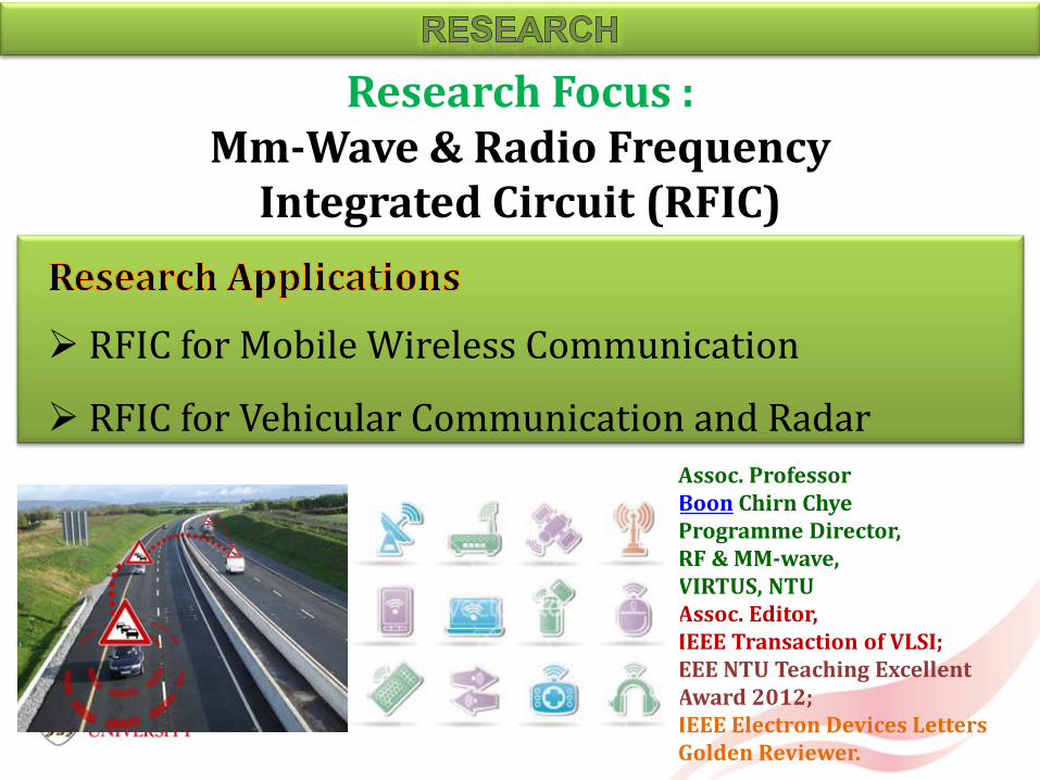
RFIC for Mobile Wireless Communication
RFIC for Vehicular Communication and Radar
Research Focus : Mm-Wave & Radio Frequency
Integrated Circuit (RFIC)
Assoc. Professor Boon Chirn Chye Programme Director, RF & MM-wave, VIRTUS, NTU Assoc. Editor, IEEE Transaction of VLSI; EEE NTU Teaching Excellent Award 2012; IEEE Electron Devices Letters Golden Reviewer.
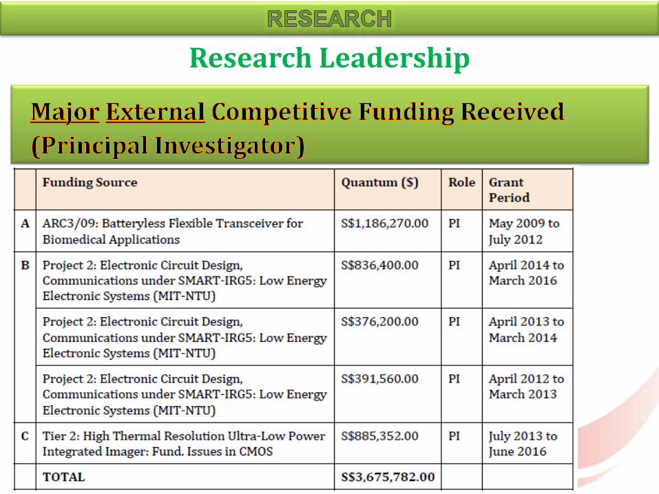
Research Leadership
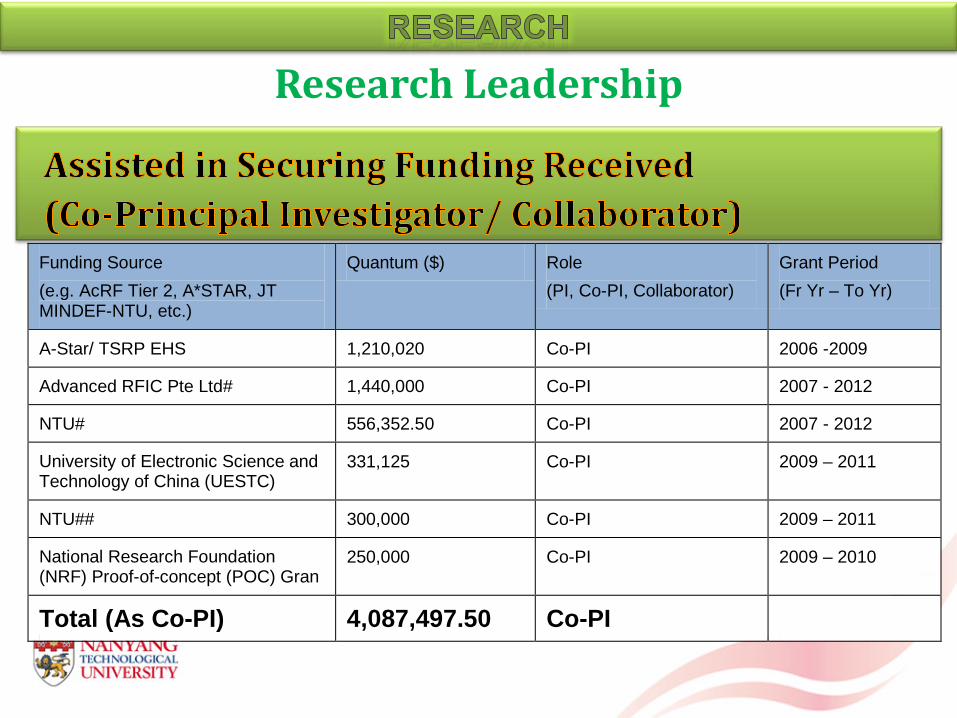
Research Leadership
Funding Source (e.g. AcRF Tier 2, A*STAR, JT MINDEF-NTU, etc.)
Quantum ($) Role (PI, Co-PI, Collaborator)
Grant Period (Fr Yr – To Yr)
A-Star/ TSRP EHS 1,210,020 Co-PI 2006 -2009
Advanced RFIC Pte Ltd# 1,440,000 Co-PI 2007 - 2012
NTU# 556,352.50 Co-PI 2007 - 2012
University of Electronic Science and Technology of China (UESTC)
331,125 Co-PI 2009 – 2011
NTU## 300,000 Co-PI 2009 – 2011
National Research Foundation (NRF) Proof-of-concept (POC) Gran
250,000 Co-PI 2009 – 2010
Total (As Co-PI) 4,087,497.50 Co-PI
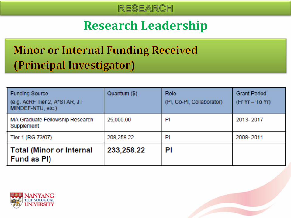
Research Leadership
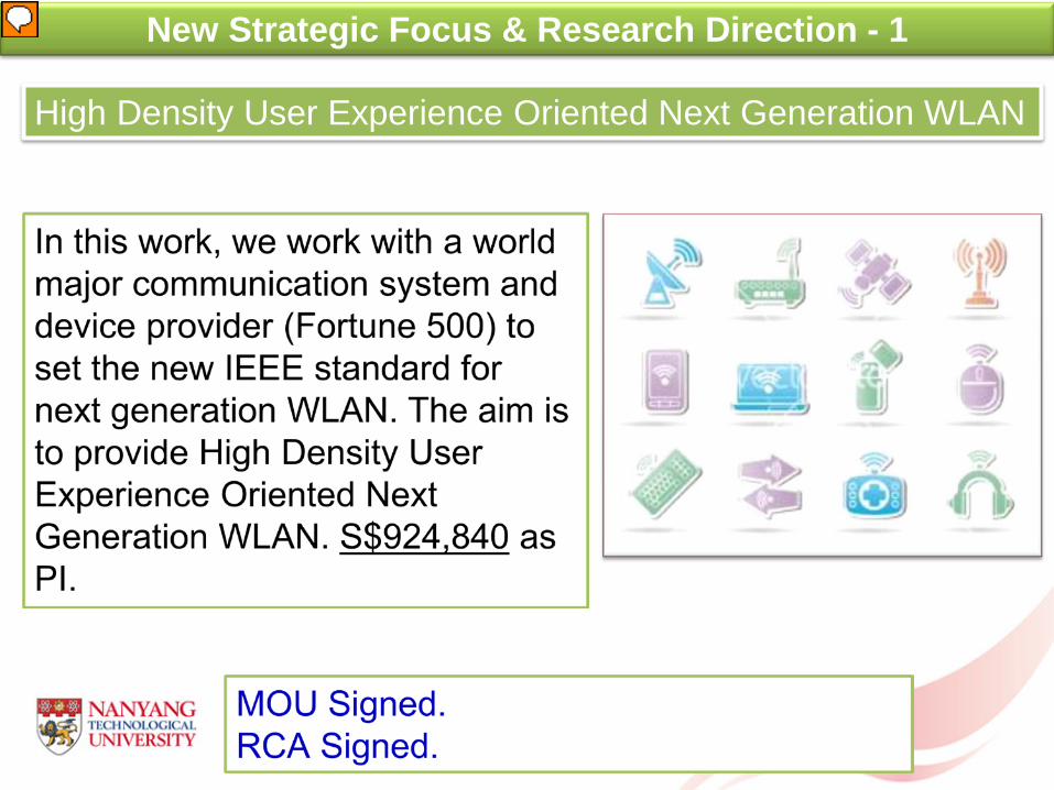
New Strategic Focus & Research Direction - 1
High Density User Experience Oriented Next Generation WLAN
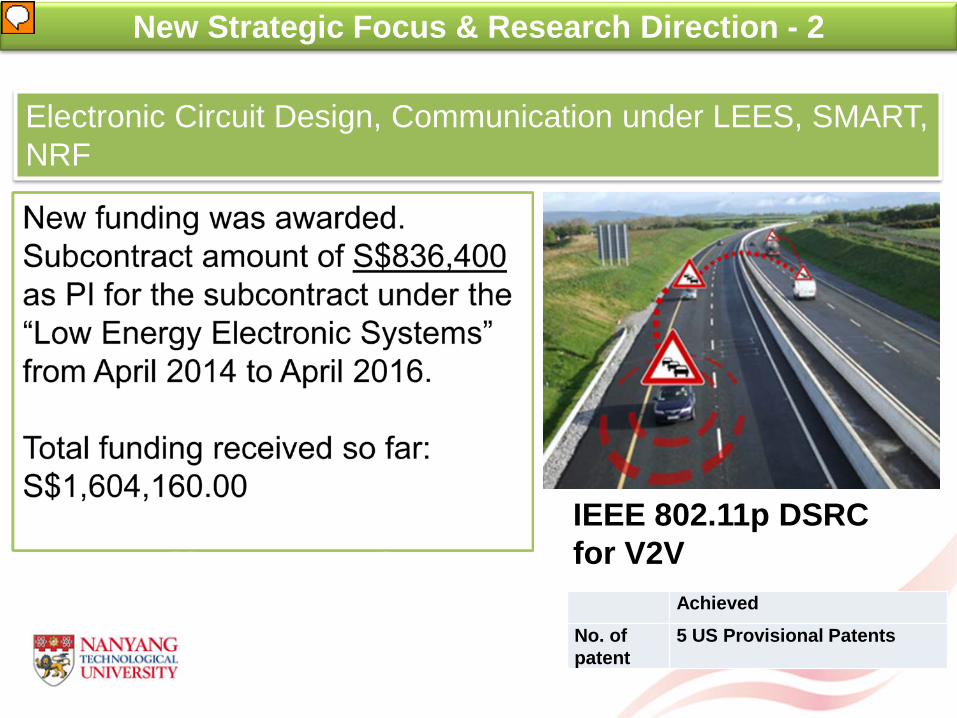
New Strategic Focus & Research Direction - 2
Electronic Circuit Design, Communication under LEES, SMART, NRF
IEEE 802.11p DSRC for V2V Achieved No. of patent
5 US Provisional Patents
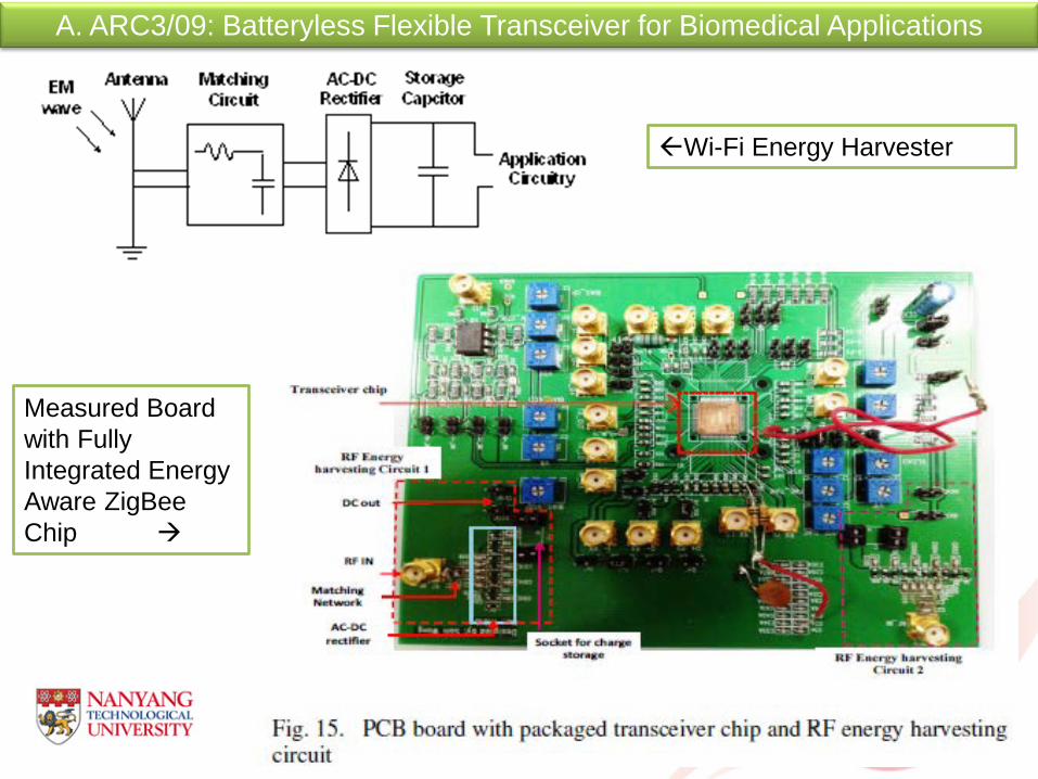
A. ARC3/09: Batteryless Flexible Transceiver for Biomedical Applications
Wi-Fi Energy Harvester
Measured Board with Fully Integrated Energy Aware ZigBee Chip
A. ARC3/09: Batteryless Flexible Transceiver for Biomedical Applications
Under my leadership, my team has conceptualized, designed and silicon-verified more than 30 RFIC circuits/chips for this topic.
This work has garnered a series of related publications including 29 top-tier journals/conferences, one book, 2 book chapters and a U.S. patent (granted).
2 invited presentation in top tier conferences (IEEE MWSCAS, IEEE RFIT).
In addition, through this project, 3 Ph.D. students and 22 Final Year Project (FYP) students were trained.
Discussion to productize this novel batteryless transceiver with Samsung is currently underway.
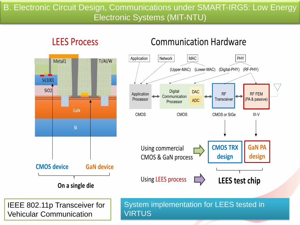
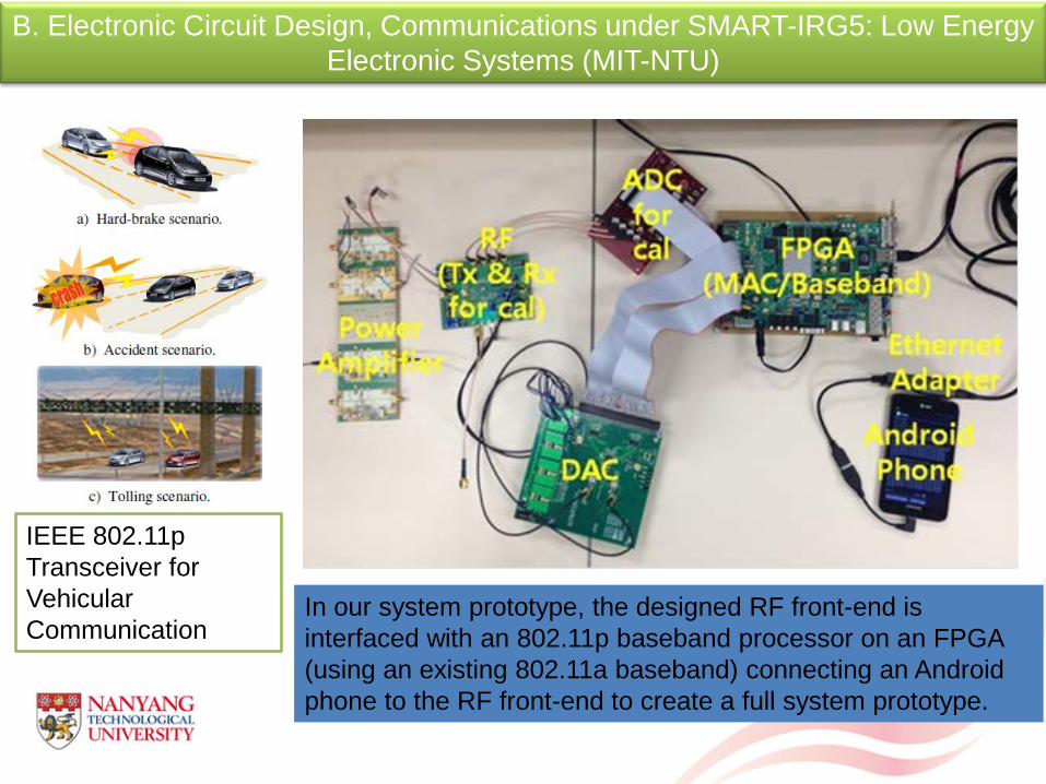
B. Electronic Circuit Design, Communications under SMART-IRG5: Low Energy Electronic Systems (MIT-NTU)
IEEE 802.11p Transceiver for Vehicular Communication
System implementation for LEES tested in VIRTUS
CMOS device GaN device
On a single die
LEES Process Communication Hardware
GaN PA design
CMOS TRX design
LEES test chip
Using commercial CMOS & GaN process
Using LEES process
B. Electronic Circuit Design, Communications under SMART-IRG5: Low Energy Electronic Systems (MIT-NTU)
IEEE 802.11p Transceiver for Vehicular Communication
In our system prototype, the designed RF front-end is interfaced with an 802.11p baseband processor on an FPGA (using an existing 802.11a baseband) connecting an Android phone to the RF front-end to create a full system prototype.
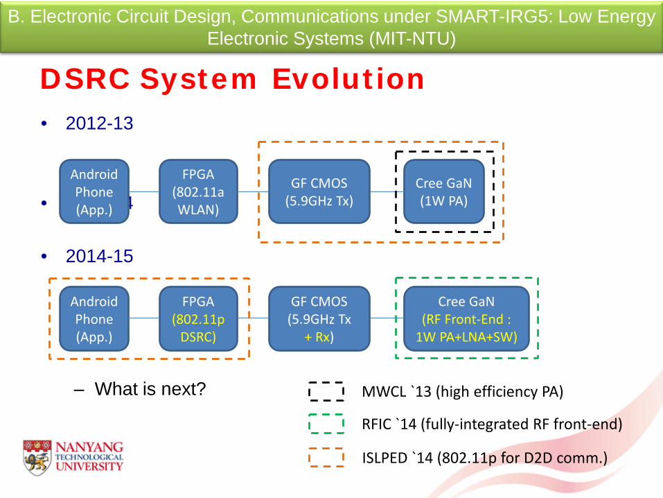
B. Electronic Circuit Design, Communications under SMART-IRG5: Low Energy Electronic Systems (MIT-NTU)
DSRC System Evolution • 2012-13
• 2013-14
• 2014-15 – What is next?
Android Phone (App.)
FPGA (802.11a WLAN)
GF CMOS (5.9GHz Tx)
Cree GaN (1W PA)
Android Phone (App.)
FPGA (802.11p
DSRC)
GF CMOS (5.9GHz Tx
+ Rx)
Cree GaN (RF Front-End :
1W PA+LNA+SW)
MWCL `13 (high efficiency PA)
RFIC `14 (fully-integrated RF front-end)
ISLPED `14 (802.11p for D2D comm.)
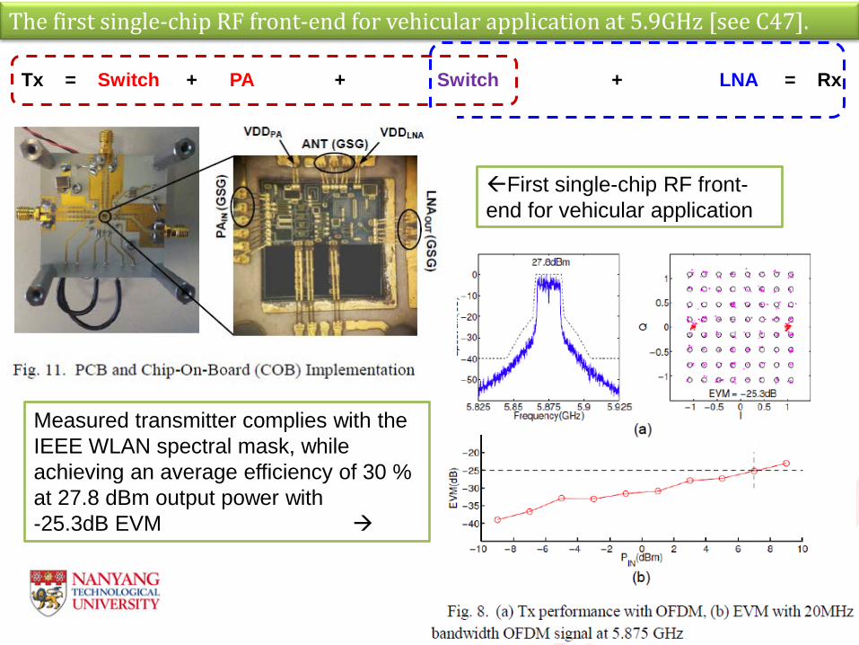
The first single-chip RF front-end for vehicular application at 5.9GHz [see C47].
First single-chip RF front-end for vehicular application
Measured transmitter complies with the IEEE WLAN spectral mask, while achieving an average efficiency of 30 % at 27.8 dBm output power with -25.3dB EVM
Tx = Switch + PA + Switch + LNA = Rx
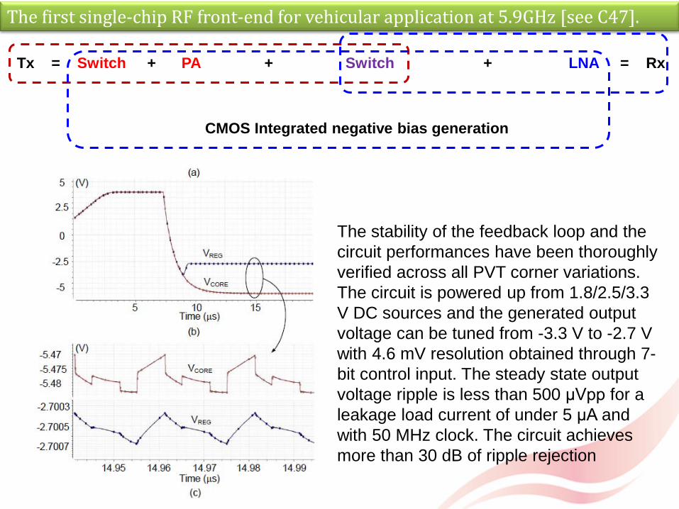
The first single-chip RF front-end for vehicular application at 5.9GHz [see C47].
Tx = Switch + PA + Switch + LNA = Rx
CMOS Integrated negative bias generation
The stability of the feedback loop and the circuit performances have been thoroughly verified across all PVT corner variations. The circuit is powered up from 1.8/2.5/3.3 V DC sources and the generated output voltage can be tuned from -3.3 V to -2.7 V with 4.6 mV resolution obtained through 7-bit control input. The steady state output voltage ripple is less than 500 μVpp for a leakage load current of under 5 μA and with 50 MHz clock. The circuit achieves more than 30 dB of ripple rejection
B. Electronic Circuit Design, Communications under SMART-IRG5: Low Energy Electronic Systems (MIT-NTU)
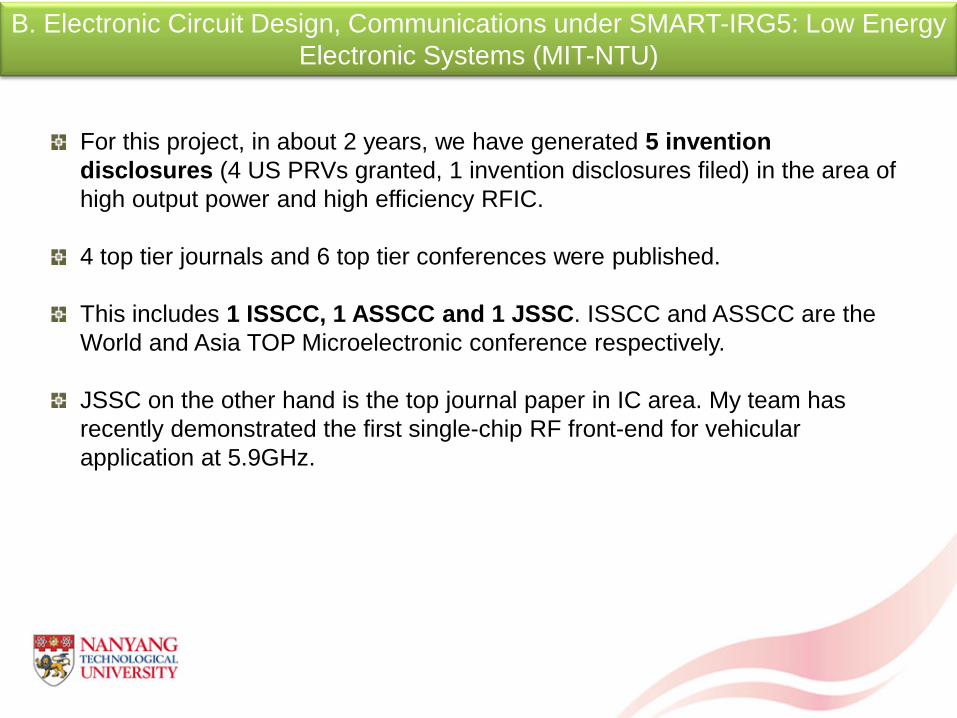
For this project, in about 2 years, we have generated 5 invention disclosures (4 US PRVs granted, 1 invention disclosures filed) in the area of high output power and high efficiency RFIC.
4 top tier journals and 6 top tier conferences were published.
This includes 1 ISSCC, 1 ASSCC and 1 JSSC. ISSCC and ASSCC are the World and Asia TOP Microelectronic conference respectively.
JSSC on the other hand is the top journal paper in IC area. My team has recently demonstrated the first single-chip RF front-end for vehicular application at 5.9GHz.
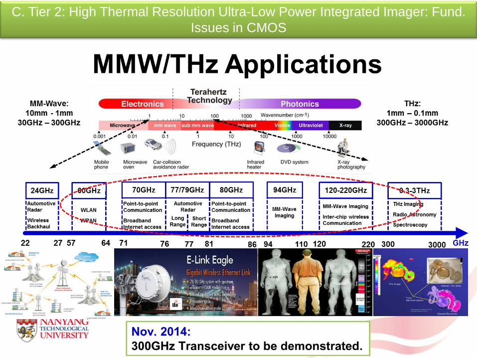
C. Tier 2: High Thermal Resolution Ultra-Low Power Integrated Imager: Fund. Issues in CMOS
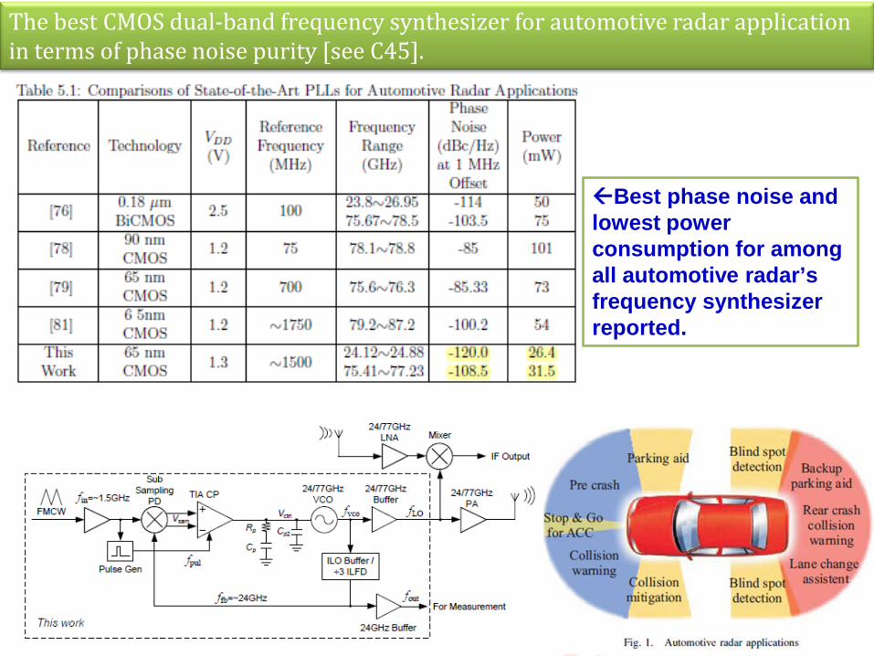
The best CMOS dual-band frequency synthesizer for automotive radar application in terms of phase noise purity [see C45].
Best phase noise and lowest power consumption for among all automotive radar’s frequency synthesizer reported.
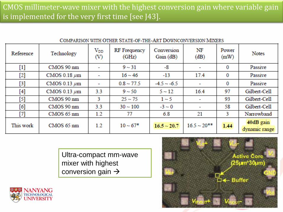
CMOS millimeter-wave mixer with the highest conversion gain where variable gain is implemented for the very first time [see J43].
Ultra-compact mm-wave mixer with highest conversion gain

Thank you for your time and effort to understand my work.