Embed Size (px)
Citation preview

THESIS ON POWER ENGINEERING, ELECTRICAL ENGINEERING, MINING ENGINEERING D24
Research, Design and Implementation of Auxiliary Power Supplies for
the Light Rail Vehicles
DMITRI VINNIKOV
TALLINN 2005

2
Faculty of Power Engineering Department of Electrical Drives and Power Electronics
TALLINN UNIVERSITY OF TECHNOLOGY Dissertation was accepted for the commencement of the degree of Doctor of Technical Science on October 17, 2005 Supervisor: Professor Tõnu LEHTLA, Ph.D. Department of Electrical Drives and Power Electronics, Faculty of Power Engineering, Tallinn University of Technology Opponents:
Professor Leonids RIBICKIS, Dr.Hab.Sc.Eng. Science Pro-Rector of Riga Technical University, Latvia Professor Marius-Paul KLYTTA, Dr.Sc. Faculty of Electrical Engineering, Giessen-Friedberg University of Applied Sciences, Germany Professor Toomas RANG, Ph.D. Head of the Department of Electronics, Faculty of Information Technology, Tallinn University of Technology Commencement: December 20, 2005 Declaration: “Hereby I declare that this doctoral thesis, my original investigation and achievement, submitted for the doctoral degree at Tallinn University of Technology, has not been submitted for any degree or examination”. Dmitri Vinnikov, ................................ Copyright Dmitri Vinnikov 2005 ISSN 1406-474X ISBN 9985-59-582-3
3
Table of Contents
LIST OF ABBREVIATIONS..................................................................................... 5 LIST OF SYMBOLS................................................................................................ 6 INTRODUCTION.................................................................................................... 7 1. ANALYSIS OF PERFORMANCE REQUIREMENTS ............................................. 15 2. STATE OF THE ART AND DEVELOPMENT TRENDS ......................................... 19
2.1 Topologies .................................................................................................... 19 2.2 Components .................................................................................................. 20 2.3 Methods of optimization............................................................................... 22 2.4 Cooling and packaging ................................................................................. 25 2.5 Generalizations of recent APS technology trends......................................... 26
3. RESEARCH OF THE ISOLATED FULL-BRIDGE DC/DC CONVERTER TOPOLOGY WITH A THREE-PHASE INTERMEDIATE AC-LINK .............................................. 28
3.1 Theoretical waveforms of the FBTP topology.............................................. 30 3.2 Comparative analysis of FBTP and FBSP DC/DC converter topologies ..... 32
3.2.1 Output filter design...................................................................................... 33 3.2.2 Inverter switch ratings ................................................................................. 36 3.2.3 Rectifier diode ratings ................................................................................. 38
3.3 Validation of predicted results by Spice modeling ....................................... 38 3.4 Final evaluation of the proposed topology.................................................... 41
4. DESIGN, IMPLEMENTATION AND EVALUATION OF A NEW APS FOR THE LRV..................................................................................................... 43
4.1 Design overview ........................................................................................... 43 4.1.1 Novelties implemented in hardware design................................................. 44 4.1.2 Proposed control method of the high-frequency inverter ............................ 47 4.1.3 Generalized mathematical model of the developed system......................... 49
4.2 Evaluative analysis of the developed system................................................ 51 4.2.1 Efficiency analysis....................................................................................... 51 4.2.2 Performance tests......................................................................................... 53 4.2.3 Final evaluation ........................................................................................... 56
5. FUTURE RESEARCH AND DEVELOPMENT ...................................................... 58 5.1 Development of APS converter for the commuter trains.............................. 58 5.2 Use of ultracapacitors in LVPS systems of LRVs ........................................ 58
CONCLUSIONS.................................................................................................... 60 REFERENCES...................................................................................................... 62 ABSTRACT ......................................................................................................... 66 KOKKUVÕTE...................................................................................................... 67 AUTHOR’S MAIN PUBLICATIONS........................................................................ 68 INTELLECTUAL PROPERTY ................................................................................ 69 LISA / ANNEX 1.............................................................................................. 70
ELULOOKIRJELDUS......................................................................................... 70 CURRICULUM VITAE ...................................................................................... 72

4

5
List of Abbreviations
AC Alternating Current APS Auxiliary Power Supply ASI Auxiliary Static Inverter AV Average value BJT Bipolar Junction Transistor CW Contact Wire DC Direct Current EMC Electro Magnetic Compatibility EMI Electro Magnetic Interference ESR Equivalent Series Resistance FBSP Full-Bridge Single-Phase isolated DC/DC converter topology FBTP Full-Bridge Three-Phase isolated DC/DC converter topology GTO Gate Turn-Off Thyristor HPDC High Power DC loads HV High Voltage I/O Input/Output IGBT Isolated Gate Bipolar Transistor IGCT Integrated Gate Commutated Thyristor IP International Protection LRV Light Rail Vehicle MTBF Mean Time Between Failures MG Motor-Generator MOSFET Metal Oxide Semiconductor Field Effect Transistor PCB Printed Circuit Board PE Power Electronics PWM Pulse Width Modulation RAMS Reliability-Availability-Maintainability-Safety RMS Root-Mean-Square value SCR Silicon Controlled Rectifier SELV Safety Extra Low Voltage SiC Silicon Carbide SMPS Switch Mode Power Supply TTTC Ltd. Tallinn Tram and Trolleybus Company Ltd. TUT Tallinn University of Technology ZCS Zero-Current Switching ZVS Zero-Voltage Switching

6
List of Symbols
a0 duty ratio of a zero state ak duty ratio of an active state An amplitude of n-th harmonic component of S (ωt) ax device’s x relative on-state time dI/dt, dU/dt current rise and voltage rise times fr ripple frequency (rectifier) fsw operating frequency (inverter) Io output current before the filter Iin (ωt) frequency spectra of the converter input current Io (ωt) frequency spectra of the converter output current before the outp.
filter IL output current (DC/DC converter) IL(max), IL(nom) maximal and nominal output currents (DC/DC converter) Isw(av) average current through the inverter switch Isw(peak) peak value of the square current pulses through the inverter switch Isw(rms) RMS current through the inverter switch Lo output filter inductor inductance LA, LB, LC leakage inductances of the primary winding (isolation transformer) La, Lb, Lc leakage inductances of the secondary winding (isolation transformer) LS main circuit wiring inductance (inverter) Pout output power (converter) px power loss of the device x Rds drain source resistance S(ωt) converter switching function ton pulse width, amount of time the power switch is on (inverter) Tpwm PWM carrier period tr(-), tr(+) voltage recovery times for the load step-up and for the load step-down Tsw operating time period (inverter) Uin(max1) continuous maximal input voltage (DC/DC converter) Uin(max2) short-term maximal input voltage (DC/DC converter) Uin(min) continuous minimal input voltage (DC/DC converter) Uin(nom) nominal input voltage (DC/DC converter) Uo output voltage of the secondary rectifier UDC DC-link voltage Uds voltage blocking capability (switch) UF on-state forward voltage drop Uin input voltage (DC/DC converter) Uin(max), Uin(min) maximum and minimum values of input voltage (DC/DC converter) Uin(nom) nominal voltage of the corresponding catenary (DC/DC converter) UL output voltage (DC/DC converter) UL(IL,max), UL(IL,min) output voltage at the full load and minimum load (DC/DC converter) UL(nom) nominal output voltage at the nominal load (DC/DC converter) Up(-),Up(+) drops and spikes in the output voltage (due to rapid load step change) Upeak peak forward voltage through the inverter switch Upri primary winding voltage vector (transformer) Zin input impedance (DC/DC converter) ZL load impedance
7
Introduction Electric traction is the only present-day solution for environmental problems in the city context. Electric traction is safe, economical, reliable and with a minimum environmental impact. The tram (or LRV, Light Rail Vehicle) is increasingly being seen as a cost-effective, environment-friendly and attractive solution to the urban transport crisis. New demands for energy efficient, reliable and safe rolling stock require purchasing of new vehicles, which is always a bulky financial burden on the rolling stock owner. In many cases, the replacement of entire rolling stock to obtain a new and more efficient technology is not economically feasible. Introduction of new energy saving technologies on old but not yet established own resource trams/LRVs in recent years has become a very attractive approach. This may be considered as a part of LRV re-manufacturing program. The purposes to be achieved for these vehicles are:
1. increased reliability, 2. reduced maintenance, 3. energy saving, 4. increased operation safety and passenger comfort, 5. meeting the requirements of a contemporary public transport system.
The auxiliary power supply converter (APS) is one of the basic systems used in rolling stock. It provides low-voltage power to every onboard electrical system and equipment on a rail vehicle, including those that are critical to its safety and operability (like brakes or lighting system). In brief, APS represents a step-down DC/DC converter, transforming high voltage from the LRV catenary (600VDC or 750VDC) to a safety low voltage (24 or 36VDC) for the onboard electric facilities. It is obvious that a failure within this system would render the whole vehicle non-operational, resulting in a financial loss, operational problems to the LRV system and discomfort to passengers. The development of APS converters began in the middle of the 1980s with the replacement of rotational converters (motor-generators) with the new fully electronical concepts (static converters). Obvious achievements like reduced weight and size, more flexible control and protection algorithms have sufficiently improved the quality and reliability of the light rail vehicles. In the course of active development of power electronic technology, size and weight parameters as well as efficiency of the LRV APS were further optimized, but output power has been remained on the level of 4...5 kW. Lately, stringent requirements for passenger safety and comfort have lead to the implementation of new onboard systems and apparatus, like more efficient hydraulic braking systems, pumps, air conditioners or even automated climate control systems, lifters for invalid chairs and perambulators, new internal lighting, etc. All of these systems, as a rule, are low-voltage fed, which finally

8
mean significantly increased power demands on the APS converter (on 2...4 or even more kW). On the other hand, the popular trend of the comfortable LRV vehicles with low floors imposes specific requirements to the design of onboard converters. With the very limited space available for the converter placement underfloor (the traditional place for the onboard electronics), power converters have to be mounted on the roofs or even inside the vehicle, which may disturb the stability of the LRV or jams the space for passengers inside it. Thus, the requirement for compact and lightweight electronics becomes very demanding especially for the new manufactured vehicles.
600VDC CATENARY (MAIN SUPPLY SYSTEM)
600V
DC P
RIM
ARY
VEH
ICLE
SUP
PLY
BUS
600VDC
LOW-VOLTAGEPOWER SUPPLY
(LVPS)
HIGH-VOLTAGEDC-FED SYSTEMS
TRACTIONDRIVE SYSTEM
VEHICLE ONBOARD SYSTEMS
LOW-VOLTAGEDC-FED SYSTEMS
SECO
NDA
RY L
OW
-VO
LTAG
E D
C SU
PPLY
BU
S BACKUP SYSTEM(ONBOARD BATTERY)
BRAKING SYSTEM
AUXILIARY SYSTEMS
MAIN SYSTEMS
HEATING SYSTEM
INFORMATIONSYSTEM
LIGHTING SYSTEM
DOORS CONTROLS
AUXILIARY DEVICES
AUXILIARYINVERTER
(ON DEMAND)
HEATINGSYSTEM
24VDC
Fig. 1. Interaction of onboard systems in the typical LRV
Thus, the development of compact, very powerful and reliable APS converter for the rail vehicles has become an essential task of any LRV-builder. According to scientific reports and conference publications, the given topic was frequently covered in the last years and as the popularity of electric transport is increasing every year, it will retain its attractiveness for the decade to come. As a result of increased interest in this specific field support from the funds of European 6th and 7th Framework Programmes has been gained. For instance, the topic of “Efficient rail traction and sustainable energy supply” has been included. In this research, studies of rail vehicles with long-term perspectives (up to 2013) will address the energy efficiency of the railway systems, considering the

9
introduction of innovative traction technologies and power converters on the rolling stock. Considering the above assumptions, the development of a completely new design for the onboard APS converter for the rolling stock application was accepted because of the following reasons:
1. Modern and future demands for the compact and powerful APS converters for new rail vehicles totally cancel a majority of recently popular designs and topologies, appealing to the development of new advanced ones. The popular and widespread APS power scheme designs (used by ABB, Vacon Traction, Elin, Enika, Koncar, Kiepe Elektrik, etc.) are very conservative and despite evident progress in semiconductors and packaging technologies not attractive for the designers. With the help of research institutions and engineering firms, LRV-builders (like Bombardier Transportation, Siemens, Alstom, etc.) have been offered an excellent possibility to obtain new advanced technologies perfectly suitable for their requirements and aspirations.
2. There are still many outdated rail vehicles using rotational converters (motor-generator systems, MG) as an onboard APS. It is obvious that a similar archaic design has many drawbacks:
• increased level of noise and vibrations; • large dimensions and weight; • low reliability and efficiency; • high maintenance costs, connected to the control and
replacement of collector brushes, control and greasing of ball bearings, balancing of rotational parts, electrical tests, etc.;
• dramatically low comfort in the passenger cabin caused by high mechanical vibrations and audible noise spreading from the MG during its operation (it is observed particularly during stops of a tram when the motor-generator achieves the maximal rotational speed in no- or light-load mode);
• low efficiency. Displacement of outdated electromechanic converters with the new energy-saving power electronic technology will be economically attractive and helps to reduce the operational and maintenance costs of the whole vehicle and to improve the comfort of passengers, which are the main priorities of any modern transportation company.
3. Railway traction with its derating reliability requirements leads to the development of robust converters, which can easily obtain new life in such prospective applications as telecommunication facilities or even the marine and aerospace industries.

10
The background of the doctoral research results from problems essential for the development of a new state of the art auxiliary power supply (APS) for the light rail vehicles (LRV):
1. many technical problems related to the specific field of use – railway transport – need to be solved. The APS for the railway traction must remain stable during serious voltage fluctuations, bad line contact, and must have high immunity to electromagnetic interference. Additionally, it must be very powerful to provide stable output voltage in very high output current variations. From another point of view, the APS must survive in different emergency situations, such as thunder, overvoltages, and short circuits in the overhead line and other circuits, etc. But the major item is that the power converter designed for the rolling stock application needs to be fully compliant with the enormous list of different norms, recommendations and regulations. To cope with those is the main task of the designer of such products.
2. Power electronic converters with the same performances meant for industrial and rolling stock applications can not be compared because of versatility of specifications and norms as well as special design requirements applied to the rolling stock ones.
3. APSs from different suppliers have different power circuit topologies, properties and dimensions. The classification and comparison of structures and power circuit topologies allow for systematizing and analyzing solutions and give a possibility to find better or newer ones.
4. The majority of advanced topologies of isolated DC/DC converters (with resonant switching, parallel/series input inverter switches or/and rectifiers, etc.), proposed and discussed on international conferences/workshops practically do not reach the market. Perfect theoretical background and simulations are not the only components of practical success. To develop an advanced power electronic technology, numerous engineering tasks need to be solved.
5. Power characteristics of the low-voltage power supply systems of the light rail vehicles can be dramatically improved. This means an improved operability and reliability of low-voltage subsystems and devices as well as extended service life of an onboard battery. The efficiency, flexibility and reliability of APS converters can be substantially optimized by help of the modern state of the art power semiconductors, packaging technologies and new semiconductor cooling methods. New solutions require theoretical and experimental investigations, analysis, comparison and optimization. However, power optimization problems related to rolling stock at the moment have been insufficiently covered in professional and scientific literature because of the high level of latent research.
6. The electronics industry is developing dynamically. Still, the new state of the art products are not fully compatible with the old ones. Problems with spare parts will occur if this issue is neglected during the design

11
and further stages. The problem on the reconstruction market is that some companies offer obsolete products with very limited possibilities, low reliability and service support.
7. There is lack of theoretical and practical knowledge in Estonia in the field of design and implementation of special power converters and systems for the rolling stock in accordance with the European norms and regulations. The transport companies need a high level competence to choose the right solutions. Detailed investigations in this area as well as development of product samples not only help to gather useful skills and experience but can improve Estonia’s positions on the European and Worldwide technology markets.
Thesis Proposal and Objectives
The main objective of the doctoral research, resulting from the problems described above is to develop and validate a new prospective DC/DC converter design for its implementation in the compact high power (≥ 6 kW) APS converter for the rolling stock application with special emphasis on specific norms and requirements. To achieve this objective, it is required to study and analyze existing systems, methods and technologies; to develop and design new technical solutions. The main research goals to be achieved are as follows:
1. analysis and systematization of the main criteria and design limitations regarding to voltage converters for the rolling stock application and their impact on the design of future systems;
2. composing of the initial task for the new APS converter design taking into account the selected limitations;
3. classification and analysis of the recent state of the art issues and current trends of similar systems to obtain reliable technical solutions for integrated and compact power scheme design, with emphasis on high integration and efficient cooling of power semiconductors, power circuits and magnetic components;
4. evaluation and recommendation of a new power circuit topology for a high power (≥6 kW) DC/DC converter for railway application, with special attention to the specific limitations (galvanic isolation) for the railway power electronic apparatus;
5. development of hardware/software models for the optimization of properties of the developed concept;
6. development of new methods and approaches for compact design; 7. design and implementation of a new APS for the LRV with improved
performance; 8. analysis and verification of the data acquired in the theoretical
investigations by the practical tests and measurements; 9. submission of final generalizations and development of proposals for
further research.

12
The following novel scientific approaches and results are proposed in the thesis:
1. classification, evaluation and comparison of structures, power circuits topologies as well as reliability, complexity, cost and other criteria. The comparison was based on the vendor's technical documentation, scientific publications and discussions with the specialists as well as on the specialized and scientific literature;
2. proposal of a new full-bridge isolated DC/DC converter topology with a three-phase intermediate AC-link as an alternative to the popular full-bridge isolated DC/DC converter topology with a single-phase intermediate AC-link for the implementation in APS system of LRV to improve efficiency and output power, minimize component stresses in high power applications and to achieve a compact design of power layout;
3. comparative analysis and evaluation of isolated FBTP- and FBSP-DC/DC converter topologies in the specific narrow application;
4. proposal of a new control method of the full-bridge isolated DC/DC converter topology with a three-phase intermediate AC-link (simplified space-vector PWM);
5. development of various models of the full-bridge isolated DC/DC converter topology with a three-phase intermediate AC-link to optimize system performance;
6. analysis and classification of performance requirements for the power converters used in rolling stock, resulting in a proposal of generalizations and recommendations for the development of appropriate designs;
7. analysis of dynamics of the LRV catenary and its impact on the operability of the APS converter;
8. analysis of dynamics of the secondary supply bus of a LRV and its impact on the operability of the APS converter;
9. analysis and systematization of the recent state of the art trends and technologies regarding to railway auxiliary power supplies; generalizations for recent technology trends;
10. proposals of practical recommendations for the development of compact high-power modular DC/DC converters for the rolling stock applications, their verification on the pilot converter;
11. analysis of losses in the implemented isolated FBTP DC/DC converter topology in different modes (with different loads);
12. analysis and methods of mitigation of common EMC problems regarding to high-frequency APS converters in rolling stock applications;
13. method of optimization of energy exchanging processes in a secondary low-voltage supply system of the LRV by help of energy storage devices (ultracapacitors);

13
14. conclusions and recommendations for further research of high-voltage high-power isolated DC/DC converters.
The direct practical values of the doctoral work are as follows:
1. energy consumption of onboard auxiliary low-voltage systems of LRV was measured and analyzed in the different operational modes. The performance tests of the rotational auxiliary power supply (motor-generator) were performed. The Tallinn Tram and Trolleybus Company Ltd. could reduce the energy consumption by the onboard auxiliary power supplies by 35% by help of the new developed system TSM1;
2. with the implemented converter TSM1 Tallinn Tram and Trolleybus Company Ltd. could minimize running, servicing and repairing costs of the APS systems by 20...50% (generally, it depends on various criteria connected to the LRV-holders themselves), resulting from the following:
• absence of DC motor brushes and full elimination of servicing; • sufficient reduction of the influence of weather conditions
(humidity, showers, snow, etc.) on the device, which increases reliability and service life;
• use of an integrated self-diagnostic system with comprehensive protection algorithms (system’s safe shutdown in dangerous situations), which guarantees system operability in all possible modes and extends system’s life substantially.
3. numerous research and development problems related to the high frequency DC/DC converter have been solved. The design of such an advanced topology links to several scientific problems. The main results of research and implemented novelties were described and analyzed in scientific and technical reports, which can be efficiently used in future research and development projects;
4. the designed, implemented and tested auxiliary power supply is very compact (15...30% reduced volume and up to 40% reduced weight in comparison with recent European analogues), very powerful (an over 50% improvement in the output current capability), has very flexible control, which allows using it with minimal changes in different LRV types and on the trolleybuses as well as in some industrial applications (welding apparatus, industrial converters, telecommunication facilities, etc.);
5. based on the positive results of this research work a business contract was concluded between the Department of Electrical Drives and Power Electronics of Tallinn University of Technology and Tallinn Tram and Trolleybus Company Ltd., providing for the production of auxiliary power supplies for trams ČKD KT4. Today nine trams of the Tallinn Tram Depot are equipped with the developed power supplies;
6. combining the energy saving traction drive developed earlier and the recently introduced control, information and diagnostic system, this auxiliary power supply can also serve as a strong basis to start

14
production of trams, trolleybuses and other electrical vehicles in Estonia as well as for retrofit applications (replacing the power supply converters on outdated vehicles);
7. an Estonian Utility Model Certificate concerning the power scheme layout, mechanical design and original control method of the developed device, was registered in the Estonian Patent Office in 2002;
Dissemination of results and publications:
1. the author has over 20 international scientific publications, 14 of those are directly connected to the topic of the doctoral research. The named have all been discussed in conferences’ reports and published in the pre-reviewed international conference proceedings. Four papers are referred in the INSPEC database and one was recommended for the publication in the IEE Journal “Electric Power Quality and Utilization” (EPQU) and provided for the IEEE Explorer database.
2. The author was granted one Estonian Utility Model Certificate (EE00331U1) for the design of the proposed system (APS converter TSM1).
3. The developed prototype has been demonstrated at the following International Exhibitions and Fairs: “11th International Power Electronics and Motion Control Conference and Fair EPE-PEMC’2005”, “Tallinn Technology Fair”, “11th European Conference on Power Electronics and Applications Conference and Exhibition EPE’2005”. The developed converter has gained interest of leading European and worldwide companies, like Bombardier Transportation, ABB Switzerland Ltd., Cegelec, Electrovypryamitel, Powertron, Alstom Belgium S.A., Ganz Transelectro Ltd., EUPEC (Infineon Group Ltd.), Elin, IXYS, WESTCODE Semiconductors Ltd., etc.
4. The results of the studies were presented and discussed in Poland, Finland, Sweden, Germany, Latvia, Lithuania, Russia, France, Croatia, and Ukraine.
5. At the beginning of 2005, negotiations with the representatives of the Ukrainian Ministry of Education and Science started at Tallinn University of Technology. Through this contact, transfer of the acquired knowledge base and technology to Ukraine is sought.
6. At the beginning of 2005, active cooperation with the Transport Department of the Tallinn City Government’s started within the European Union 6th and 7th Framework Programs, for example, in such areas as “Efficient Rail Traction and Sustainable Energy Supply” or “Low-Cost Power-Integrated Advanced Hybrid Configurations”.

15
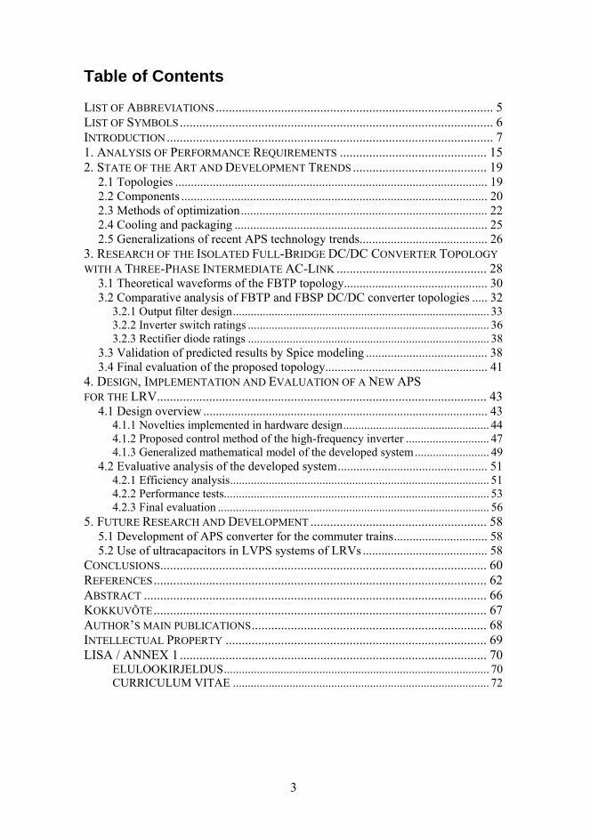
1. Analysis of Performance Requirements During the development of any new product or system, there are some limitations a designer must cope with. In the design of the APS for the rolling stock, the basic factors, which are becoming increasingly important, are divided into two groups (Fig. 2).
LIMITING FACTORS OF THE RAILWAY
CONVERTER DESIGN
REQUIREMENTS/ ASPIRATIONS OF END-USER
SPECIFIC RAILWAY REQUIREMENTS/
LIMITATIONS
• Low cost and time to build• Low cost of ownership • Improved efficiency • Small overall dimensions • Low weight • Low noise level
• Compliance with supply voltage requirements
• Compliance with dynamic performance requirements
• Compliance with EMC requirements
• Compliance with electric safety requirements
• Compliance with reliability requirements
Fig. 2. Classification of limiting factors for the APS converter design
While aspirations of end-users (rolling stock owners) are always directly connected to a better price-quality ratio of the new device (which helps to improve the economical efficiency of the developed or renovated object), the most challenging part for the designer are the limitations coming from the specific field of use - rolling stock. In general, main recommendations and limitations to be fulfilled are submitted in more than 20 European and international standards. These performance standards are defined practically for every facet of a railway operational environment, including shock, vibration, extended temperature range, humidity, salt, fog, load and voltage fluctuations and many more. By the synthesis of the standards and directives, the design of new APS for the rolling stock needs to be coordinated in accordance with key-issues, presented in Fig. 2 (right column). The classification and analysis of railway converter performance requirements are shown in Fig. 3. Despite all the presented railway converter performance requirements that directly influence the converter design, compliance with electric safety requirements and with reliability requirements is crucial. The first requirement provide specific features of the power circuit topology of an APS converter, requiring an isolation transformer to decouple input and output sides (with an isolation test at least 2.1kVDC/1min). In accordance with this limitation, the required generalized block diagram of the power circuit topology for APS converters for the rolling stock is proposed in Fig. 4. Since the isolation transformer in switching-mode power supplies contributes about 25…30% of the overall volume and more than 30% of the overall weight [PET95], the design of the compact and lightweight system will be a great challenge for the designer.
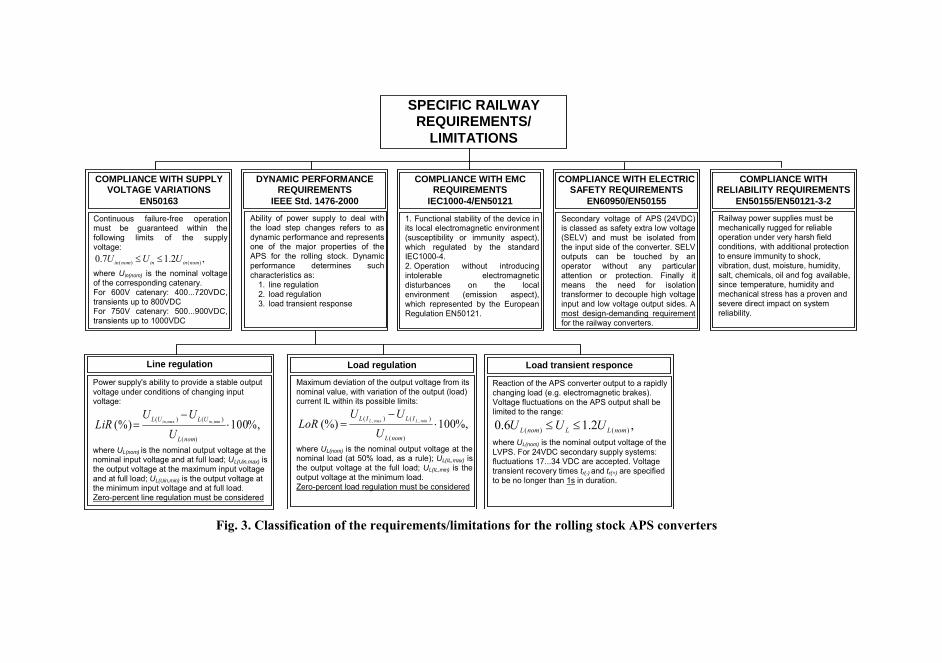
SPECIFIC RAILWAY REQUIREMENTS/
LIMITATIONS
COMPLIANCE WITH SUPPLY VOLTAGE VARIATIONS
EN50163
DYNAMIC PERFORMANCE REQUIREMENTS
IEEE Std. 1476-2000
COMPLIANCE WITH EMC REQUIREMENTS
IEC1000-4/EN50121
COMPLIANCE WITH ELECTRIC SAFETY REQUIREMENTS
EN60950/EN50155
COMPLIANCE WITH RELIABILITY REQUIREMENTS
EN50155/EN50121-3-2
Continuous failure-free operation must be guaranteed within the following limits of the supply voltage:
,2.17.0 )()( nomininnomin UUU ≤≤ where Uin(nom) is the nominal voltage of the corresponding catenary. For 600V catenary: 400...720VDC, transients up to 800VDC For 750V catenary: 500...900VDC, transients up to 1000VDC
1. Functional stability of the device in its local electromagnetic environment (susceptibility or immunity aspect), which regulated by the standard IEC1000-4. 2. Operation without introducing intolerable electromagnetic disturbances on the local environment (emission aspect), which represented by the European Regulation EN50121.
Secondary voltage of APS (24VDC)is classed as safety extra low voltage (SELV) and must be isolated from the input side of the converter. SELV outputs can be touched by an operator without any particular attention or protection. Finally it means the need for isolationtransformer to decouple high voltage input and low voltage output sides. A most design-demanding requirementfor the railway converters.
Railway power supplies must be mechanically rugged for reliable operation under very harsh field conditions, with additional protection to ensure immunity to shock, vibration, dust, moisture, humidity, salt, chemicals, oil and fog available, since temperature, humidity and mechanical stress has a proven and severe direct impact on system reliability.
Ability of power supply to deal with the load step changes refers to as dynamic performance and represents one of the major properties of the APS for the rolling stock. Dynamic performance determines such characteristics as:
1. line regulation 2. load regulation 3. load transient response
Line regulation
Power supply's ability to provide a stable output voltage under conditions of changing input voltage:
%,100(%))(
)()( min,max, ⋅−
=nomL
ULUL
UUU
LiR inin
where UL(nom) is the nominal output voltage at the nominal input voltage and at full load; UL(Uin,max) is the output voltage at the maximum input voltage and at full load; UL(Uin,min) is the output voltage at the minimum input voltage and at full load. Zero-percent line regulation must be considered
Load regulation
Maximum deviation of the output voltage from its nominal value, with variation of the output (load) current IL within its possible limits:
%,100(%))(
)()( min,max, ⋅−
=nomL
ILIL
UUU
LoR LL
where UL(nom) is the nominal output voltage at the nominal load (at 50% load, as a rule); UL(IL,max) is the output voltage at the full load; UL(IL,min) is the output voltage at the minimum load. Zero-percent load regulation must be considered
Load transient responce
Reaction of the APS converter output to a rapidly changing load (e.g. electromagnetic brakes). Voltage fluctuations on the APS output shall be limited to the range:
,2.16.0 )()( nomLLnomL UUU ≤≤ where UL(nom) is the nominal output voltage of the LVPS. For 24VDC secondary supply systems: fluctuations 17...34 VDC are accepted. Voltage transient recovery times tr(-) and tr(+) are specified to be no longer than 1s in duration.
Fig. 3. Classification of the requirements/limitations for the rolling stock APS converters

17
CONTROLSYSTEM
INPUTFILTER
INVERTER-STAGE
ISOLATIONTRANSFORMER
RECTIFIER-STAGE
OUTPUTFILTER
GALVANICISOLATION
GALVANIC ISOLATION
INDICATES POWER FLOW
INDICATES SIGNAL FLOW
INPUT DC VOLTAGE
OUTPUT DCVOLTAGE
OUTPUT VOLTAGE ANDCURRENT FEEDBACKS
INPUT VOLTAGEFEEDBACK
CONTROL OF INVERTERSWITCHES
DC AC AC DC
Input side Intermediate AC link Output side
Special requirement by
EN 60950/EN50155
Fig. 4. The required structure of the onboard APS converter for the rolling stock
Reliability requirements are mostly oriented to the proper selection of components and design of mechanical construction and cooling, because an APS converter must be able to operate for 24 hours daily for 30 years, which means MTBF of approx. 250,000 hours. In fact, these stringent and comprehensive requirements are needed because the failure of an electronic assembly in a passenger rail transport could jeopardize human lives. Finally, it means that power electronics for railway transport is more complicated than for industrial applications. Many traditional converter designs as well as components and technologies will fail in this demanding application. The major challenges for the proper APS converter design for the rolling stock application are represented in Fig. 5.
CONTROLSYSTEM
INPUTFILTER
INVERTER-STAGE
ISOLATIONTRANSFORMER
RECTIFIER-STAGE
OUTPUTFILTER
GALVANICISOLATION
GALVANICISOLATION
INPUT DC VOLTAGE OUTPUT DC
VOLTAGE
OUTPUT VOLTAGE ANDCURRENT FEEDBACKS
INPUT VOLTAGEFEEDBACK
CONTROL OF INVERTER SWITCHES
DC AC AC DC
Challenges:Power switches with increased Uds (≥1200V)
Challenges: Increased rated and surge voltage levels of elements
Challenges:Faster CS for better line/load regulation and transient responce
Challenges:Better isolation coordination (≥2100VDC/min)
Challenges:Faster power switches (better dI/dt and dU/dt)
Challenges:Soft start capability during catenary interruptions or sags
Challenges:Optimized secondary wiring (lower voltage drop an high loads)
Challenges:Faster rectifier diodes with minimal forward voltage
Challenges: Lower voltage and current ripple, lower voltage drop
Challenges: Cooling methods, loss minimization, materials, level of integration
Challenges:EMC immunity, galvanic insulation, power consumption
Challenges:Casings with high IP level, humidity resistance, improved cooling
Challenges: Low-inductive packaging, integration, efficiency
OVERALL DESIGN GOALS:
• Weight, size • Reliability • Cost
Challenges: Ambient temperatures range: -25...+70 0C, Shock protect.:981m/s2
Cont. shock: 392m/s2
Vibration prot.:49m/s2
Fig. 5. Design challenges to the APS converter for rolling stock applications A detailed analysis of operational conditions, requirements and aspirations of the end-user provides a strong support to the selection of an optimal (right) converter design so as to prevent possible troubles and failures. Namely, this stage is most demanding within the whole serial process of the development of new APS for the rolling stock application (Fig. 6).

18
START OFDEVELOPMENT
ANALYSIS OF END-USERREQUIREMENTS AND
ASPIRATIONS
ANALYSIS OF SPECIFICREQUIREMENTS AND
LIMITATIONSCONCERNING
APPARATUS FOR THEROLLING STOCK
FUNCTIONAL ANALYSIS OFSYSTEM TO BE DEVELOPED
SYNTHESIS OFPOSSIBLE TOPOLOGIES
AND/OR ACCEPTABLESOLUTIONS
EVALUATION ANDDECISION
SELECTEDCONCEPT
EVALUATION ANDSELECTION OFCOMPONENTS
GENERALSPECIFICATIONS
REQUIREDSPECIFICATIONS
FULFILLED?
Yes
DEVELOPED PILOTCONVERTER
ELECTRICAL ANDMECHANICAL DESIGN
TESTING AND FINALEVALUATION
ESTABLISHEDDESIGNER’S TASKS
FULFILLED?
No
BUILD-UP
No (low reliability,EMC problems,
overheating, etc.)
No (high weight,size, cost, noisy)
READY-FOR-MANUFACTURING
PRODUCT
COMPLIANT WITHRAILWAY EMC ANDELECTRIC SAFETYREQUIREMENTS?
No
Yes
Red
esig
n R
edes
ign
Red
esig
n
DESIGN OPTIMIZATION
OFFICIAL VALIDATION
ANALYTICAL STAGE - MOST DEMANDING
PRACTICAL STAGE
Fig. 6. Representation of a serial development process of APS for the rolling stock

19
2. State of the Art and Development Trends Design of APS converter is crucial because of the high level of complexity, integrity, importance and requirements applied to its properties. Additionally, studies of high- and medium-power DC/DC converters for the railway applications are attracting wider interest because of the high level of privacy and existing technological rivalry between research companies and institutions in this specific field. The majority of the conference and journal articles and research reports about the DC/DC converters are related to low-power conversion with input voltage levels up to 100 VDC or power ratings of several hundred watts. Technology progress in this field in the last five years is more than obvious, but the collected know-how is not directly applicable to the demanding area of rolling stock with high power ratings and voltage conversion ratios. Thus, studies of converter techniques within the railway sector will be a leading direction of power electronics development in the near decade.
2.1 Topologies In the evaluation of schematics of the different state of the art products it is desirable to pay attention to the topologies of both switching stages (inverter and rectifier), because they are main contributors in total power loss, especially in high frequency operation.
Inverter-stage topologies
Although the selection of proper topology for the cost minimization by the logical way needs to be done from the simplest topologies, the rugged railway limitations involve own orders. The need for DC/DC converter with galvanic isolation reduces the designer’s choice to the group of isolated topologies. Fig. 7 illustrates mostly used isolated converters’ family tree. This includes two main subgroups: single switch isolated DC/DC converter topologies and multiple switch isolated DC/DC converter topologies.
ISOLATED SWITCHED-MODE DC/DCCONVERTER TOPOLOGIES
MULTIPLE SWITCHSINGLE-SWITCH
FLYBACK ĆUKBOOST
DISCONTINUOUSMODE
CONTINUOUSMODE
FULL-BRIDGE HALF-BRIDGE(up to 3 kW)
PUSH-PULL(up to 3 kW,
low voltage input)
SINGLE-PHASEINTERMEDIATE AC
LINK(up to 5 kW)
MULTI-PHASEINTERMEDIATE
AC LINK(>5 kW)
TWO-SWITCHFORWARD(up to 2 kW)
FORWARD
MOST POPULAR IN RAILWAY
APPLICATIONS
HAS NOT EVER BEEN PROVED IN RAILWAY
APPLICATIONS Fig. 7. Classification of basic isolated DC/DC converters topologies
So far, suitable topology during the development of an APS for the LRV was selected from three single-phase multiple-switch topologies: two-switch forward

20
[TRI97], [LEU01], half-bridge [HAR98] and full-bridge [ČOB02], [AKH93], [MOH03] (selected area on the Fig. 7). From the point of view of efficiency and robustness, the full-bridge topology must be denoted as the best choice over others for the inverter-stage. For that reason the single-phase topology is the most popular and the highly widespread DC/DC converter topology for the rolling stock auxiliary DC power supplies.
Rectifier-stage topologies
Fig. 8 demonstrates most widespread rectifier configurations for secondary-side rectification. Each secondary-side rectification has its advantages and disadvantages, which were discussed in detail in different publications [DON02], [MIN04], [ROE01], etc.
RECTIFIER STAGE TOPOLOGIES
UNCONTROLLED HALF-CONTROLLED
SINGLE-PHASE POLYPHASE
HALF-VAWE FULL-WAVE
CONTROLLED
THREE-PHASEHALF-WAVE
STAR
THREE-PHASEFULL-WAVE
BRIDGE
CENTER-TAPPED FULL-BRIDGE
CURRENT-DOUBLER
THREE-PHASEFULL-WAVE
STAR
THREE-PHASE DOUBLE-WYE WITH INTERPHASE
TRANSFORMER
SIX-PHASE STAR SIX-PHASE
FULL-WAVE
Fig. 8. Classification of main secondary rectifier topologies
It is well understood that certain secondary-side topologies are deemed less desirable in the specific railway applications. Rectifier-stage designs have to be used (or presented in the schematics) in the last decade for the low- and middle-power APS for the LRV mainly evolve around three uncontrolled single-phase topologies: center-tapped full-wave ([AKH93], [HAR98]), current-doubler [ČOB02], [BAL01] and full-bridge full-wave [DON02] rectifiers. Controlled rectifiers are not used because of unidirectional energy flow (input→output) required from APS converters.
2.2 Components The particular components used within switching power converters greatly affect their performance. The selection of the switching and rectifying elements, the magnetic components and the filter capacitors greatly influences the switching frequency, efficiency and the performance of the whole converter.
Power semiconductors
Rail traction exerts many special requirements for the primary inverter switches; one of those is the need for high-voltage blocking capabilities (at least 1200V in 600VDC LRV catenaries). The first generation of switched-mode DC/DC converters used Gate Turn-off Thyristors (GTO) and Bipolar Junction Transistors (BJT) as primary switches. However, the development of converters over the last five years was dominated by the evolution of IGBT (Isolated Gate

21
Bipolar Transistor). The IGBT rapidly replaced all the prior GTOs and BJTs. Advancements and trends in modern semiconductors for primary inverters are compared in Fig. 9 ([SCH02], [MIT00], [ABB02], [IXY05], [NIK00] and [BAU01]).
12000V/1500A (Mitsubishi)
1650A/7500V (Eupec)
2650A/ 6500V(ABB)
2300A/5500V(ABB)
4000A/4500V(Mitsubishi)
5000A/4800V(Westcode)
6000A/6000V(Mitsubishi)
600A/6500V (Eupec)
1200A/3300V(Eupec)
1800A/2500V(Fuji)
2400A/1700V(Eupec)
0
2000
4000
6000
8000
10000
12000
14000
0 1000 2000 3000 4000 5000 6000 7000
U,V
I,A
On-market SCRs
On-market GTOs
On-market IGCTs
On-market IGBTs
Minimal accepted Uds (1200V)
Fig. 9. Power range envelopes of available primary switch technologies
The IGBT, due to its availability, ease of use, efficiency and cost efficiency, will be the device chosen for the next 5 to 10 years of railway power conversion equipment design and manufacture.
Capacitors
During the last 15 years, the only choice was to use electrolytic capacitors (connected in parallel or series to achieve desired DC-link voltage of capacitance values). But the current trend of traction market for power conversion is to replace electrolytic capacitors by film technology [AWX04], [TOL04]. This trend is generated by many advantages that film technology is offering (Table 1). Table 1. Comparison of characteristics among various kinds of DC-link capacitors
Item Electrolytic technology Film technology Miniaturization Superior Inferior Frequency characteristics Inferior Superior Temperature characteristics Inferior Moderate High voltage Moderate Superior High capacity Superior Moderate Service life Inferior Superior Cost/capacity ratio Superior Inferior

22
However, despite their clear advantages, film-type capacitors are seldom used in place of electrolytics today, because they are more expensive, and their smaller bus capacitance provides less drive ride-through protection during utility voltage sag events.
Isolation transformers
Up to today, the most relevant trend was to use laminated isolation transformers with the excitation frequencies around 400 Hz. Toroidal-form transformers are a new trend for system weight/space minimization. Common evaluations of laminated and toroidal transformers were presented in several publications [KHA94], [PET95], but the benefits of toroidal ones are lower off-load power consumption (Fig. 10, a) and weight/volume (Fig. 10, b and c).
0
75
150
225
300
0 1 2 3Power Rating (kVA)
Off
- loa
d po
wer
(VA
)
Laminated Toroidal
0
2.5
5
7.5
10
0 1 2 3Power Rating (kVA)
Volu
me
Laminated Toroidal
(m3 , x
10-3
)
(a) (b)
0
4
8
12
16
0 1 2 3
Power Rating (kVA)
Wei
ght (
kg)
Laminated Toroidal
(c)
Fig. 10. Comparison of laminated and toroidal transformers
2.3 Methods of optimization
Increased switching frequency
The main trend in the design of onboard APS for the rolling stock in the last years was aimed at improvements in power density (volume-output power ratio) and a better system integrity by means of increased switching frequency of the primary inverter (from 50...100Hz to 400...1000Hz and even higher). However, with the higher switching frequency, the converter usually needs a larger heatsink (because the switching losses of semiconductors are direct-dependant with switching frequency) to provide the optimal temperature mode for the semiconductors, and, thus, to obtain the necessary reliability of the whole device. Up to now, selection of proper switching frequency is always a tradeoff for the designer (Fig. 11) but typically limited by the properties of inverter power switches by 20 kHz in a hard switching mode (Table 2).
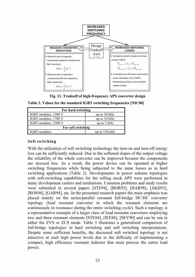
23
REDUCED CONVERTER WEIGHT/SIZE
• Reduced size of magnetic
components (isolation transformers,
filter inductors):
fLILP 2
21)( =
• Reduced size of capacitive
components (DC-link capacitors,
filter capacitors):
fCUCP 2
21)( =
INCREASED SWITCHING LOSSES
• Increased dynamic losses of primary
inverter IGBTs:
onturnswonturn EfP −− ×= offturnswoffturn EfP −− ×=
• Increased turn-off losses and forward
power dissipation of an IGBTs,
freewheeling diodes and secondary
rectifier diodes
Design Tradeoff???
INCREASED SWITCHING FREQUENCY
Fig. 11. Tradeoff of high-frequency APS converter design Table 2. Values for the standard IGBT switching frequencies [NIC00]
For hard switching IGBT-modules, 1200 V up to 20 kHz IGBT-modules, 1700 V up to 10 kHz IGBT-modules, 3300 V up to 3 kHz
For soft switching IGBT-modules up to 150 kHz
Soft switching
With the utilization of soft switching technology the turn-on and turn-off energy loss can be sufficiently reduced. Due to the softened slopes of the output voltage the reliability of the whole converter can be improved because the components are stressed less. As a result, the power device can be operated at higher switching frequencies while being subjected to the same losses as in hard switching applications (Table 2). Developments in power scheme topologies with soft-switching capabilities for the rolling stock APS were performed in many development centers and institutions. Common problems and study results were submitted in several papers [STE94], [BOR95], [HAR98], [AKH93], [ROS98], [GAR94], etc. In the presented research papers the main emphasis was placed mainly on the series/parallel resonant full-bridge DC/DC converter topology (load resonant converter in which the resonant elements are continuously in resonance during the entire switching cycle). Such a topology is a representative example of a larger class of load resonant converters employing two and three resonant elements [STE84], [IEE88], [SEV90] and can be run in either the ZVS or ZCS mode. Table 3 illustrates a generalized comparison of full-bridge topologies in hard switching and soft switching interpretations. Despite some sufficient benefits, the discussed soft switched topology is not attractive at such high power levels due to the difficulty of implementing a compact, high efficiency resonant inductor that must process the entire load power.

24
Table 3. Evaluative analysis of FBSP topologies in hard and soft switching modes
Characteristic Hard switched full-bridge
Soft switched full-bridge
Control complexity Simple Moderate Constant frequency Yes No Circulating current No Yes Primary switch stresses High Moderate Output rectifier stresses High Low Ripple current in Co Low Low Resonant inductor No Bulky Resonant capacitor No Bulky
Thus, despite several obvious advances in soft switching converters, modern trends in the design of voltage converters for the rolling stock are directed to the hard switching techniques. Soft-switching techniques definitely bring benefits to DC/DC converter design, but they also bring penalties which include complexity and component costs. Nowadays, the overall simplicity of the hard switching strategy is the key-factor for the designer. The high level of complexity of the power scheme with resonant switching may entail the increased cost and decreased reliability of the developed device.
Advanced rectifiers and synchronous rectification
The previous generation of APS for the LRV, as a rule, was mainly equipped with the low-frequency rectifiers, which were built on the traditional discrete diodes or diode modules (with on-state forward voltage drop UF=1.5…2V). The new challenge is to replace the traditional silicon diodes by more advanced ones. Thus, Schottky diodes (Fig. 12) or fast switching diodes have already allowed the achievement of remarkable benefits [IXY05]. Both presented types have essentially lower voltage drops in the on-state condition. For instance, the 0.2…0.5V voltage drop of a Schottky diode and about a 0.9…1.0V voltage drop in the case of fast recovery diodes [GUE00] help to improve the efficiency of the rectifier stage by 30-50%.
Schottky18%
Ultrafast19%
Standard43%
Other1%
Fast19%
Fig. 12. Recent in-use types of diodes
Hence, there is a certain number of limiting characteristics concerning the use of new rectifiers. The reverse voltage of a Schottky diode is usually less than 200V and a fast-recovery diode, as a rule, still has a reverse recovery time that is
25
moderately long. It is only the utilization of the advantages of switching transistors (simple drive, short switching times and high reverse voltage capability) as rectifiers that has led to the latest trend in the modern DC/DC converters [ZWI98], [BLA94], [FER94], [FUK95]. Synchronous rectifiers are realized on MOSFET switches. Thus, operating in the MOSFET III quadrant, a synchronous rectifier presents resistive VA-characteristics (Fig. 13). Under certain current level (≤35...50A), the forward-voltage drop of a synchronous rectifier can be lower than that of a diode rectifier, and consequently, further reduces the rectifier conduction loss. Due to the fact that synchronous rectifiers are active devices, the design and utilization of synchronous rectification need to be properly addressed.
0
10
20
30
40
50
0 0.1 0.2 0.3 0.4 0.5 0.6 0.7
VF (V)
I F (A
)
Diode Rectifier Synchronous Rectifier Fig. 13. Forward-voltage drop comparison between a synchronous rectifier
and a diode rectifier
As reported in the majority of research papers, synchronous rectification gives a real advantage in low-voltage (UL≤15V) low-current (IL≤50A) applications, while in APS converters with output currents greater than 100A fast diodes are an absolutely dominant solution.
2.4 Cooling and packaging Cooling and packaging of power converters are two very demanding factors in the rolling stock application. Harsh ambient conditions in a row with rapidly changing operation modes (deep variations of voltages and loads) may considerably reduce the MTBF (lifetime) of power electronic device. For the end-user, the combination of high power and efficiency and small space requirement is very desirable. However, the electronics engineer has to deal with the problem of how to dissipate the large amount of waste heat. As packages become smaller, achieving efficient thermal performance for power applications requires that the designers employ some new efficient methods of meliorating the heat flow out of devices [KEL00], [BAK00]. The classification and comparative analysis of general cooling methods in modern power converters is given in Fig. 14. Up to recent time, the most relevant trend for low- or middle-power APS converters for the rolling stock was to use natural convection [ČOB02]. Today’s increased power demands and requirements for compact designs need new more efficient ways of cooling. Basically it means forced convection [KEL00],

26
[FIS05], [VOS92], which represents a best alternative in terms of thermal efficiency-complexity ratio for such amount of transferred power (3-10kW).
Extrusions
Stampings
NATURAL CONVECTION
Hollow fin cooling aggregates
Fan heatsinks High fin density assemblies
FORCED CONVECTION
Large diameter heat pipe assemblies Small diameter heat pipe assemblies
FLUID PHASE CHANGE
Large diameter heat pipe assemblies Small diameter heat pipe assemblies
LIQUID COOLED
Ther
mal
Effi
cien
cy
Com
plex
ity
Heat dissipation capability Low High
High High
Low Low
New prospective technology
Fig. 14. Comparative analysis of general cooling methods of power converters
2.5 Generalizations of recent APS technology trends To obtain information about the technologies implemented and recent APS design solutions, four different industrial APS converters for LRVs from several European industrial companies have been compared in principle (Table 4). Table 4. Technology comparison of several APS converters
Based on the data presented in Table 4, it is remarkable that in low- or medium-power conversion the IGBT has basically replaced other alternative power switch technologies. As a rule, hard switching of IGBTs is used for the simplification of the power circuit and, finally, the price of the final device. The
Vacon Traction, 5TX600 120(160)
DCDC600
Koncar Company, Battery Charger
150 A, 24 V
Kiepe Elektrik, BNU100/ BNU300
Enika, ENI-
PT600/24/AC
Inverter-stage topology
single-phase bridge
single-phase bridge
single-phase bridge
single-phase bridge
Inverter-stage semiconductors IGBT IGBT GTO, IGBT IGBT
Type of switching hard sw. hard sw. hard sw. hard sw.
Switching frequency, kHz 0.4 20 n.a. n.a.
Rectifier-stage topology center-tapped current-doubler full-bridge center-tapped
Rectifier-stage semiconductors diode diode diode diode
Cooling type forced convection natural convection natural/forced convection natural convection
Weight, kg 100 n.a. 170/170+ 90

27
dominant power scheme topology is the single-phase bridge. No technologies (soft-switching, synchronous rectification), allowing for improvement of the efficiency were identified. The main trend is the system simplification, which overcomes such criteria as operability and flexibility.
Generalizations of recent APS technology trends
It can be concluded that the performance improvement in efficiency and power density can be achieved only by the improvements in semiconductors, magnetic components, capacitors, and cooling/packaging. The topologies can not be easily judged by themselves, rather the whole design, implementation and finally cost versus performance should be considered. Based on the analysis of technological achievements in converters and power electronic apparatus for the rolling stock application in the last decade, the main trends can be summarized as follows:
1. voltage-fed converters using force-commutated thyristors are already obsolete in LRV APS applications. Nobody should plan building them. This means that inverter-grade thyristors have no future in this field.
2. IGBTs have the potential to fully replace GTOs since they allow substantial cost savings due to snubberless operation and simple control.
3. Power MOSFETs will remain as viable devices in low-voltage low-power high frequency applications (Uds(max)≤1000V, which are not acceptable for catenary-fed railway converters with the Uds(max)≥1200V ).
4. At the moment the defect density of SiC wafers as well as the high manufacturing price is two limiting factors for an introduction of this prospective technology to railway voltage converters.
5. New state of the art rectifiers (Schottky, ultrafast- and fast-recovery diodes, etc.) supersede older ones, which help to lift the system efficiency on the new level.
6. Railway converters still have a tendency for the simplification of the power scheme, with minimized amount of functional elements and easy control, because the reliability will remain as a general target.
7. Advanced allowing improvement of the efficiency technologies, like synchronous rectification or soft switching, are unacceptable in catenary-fed converters, because of complexity and high implementation cost.
8. In a row with improvements in power semiconductors the cooling of railway converters will remain one of significant targets, because it is the second general way of improving power density and reliability.
9. The majority of available ready-to-use converters are very similar - a conservative design of power stage based on non-advanced elements and technologies leads to lack of operability (converters have very limited output current capability and may be mostly referred as battery chargers, not APS), low efficiency (such factor is very confidential, however, typically it is in the range of 75-85%), large weight and dimensions and lack of flexibility (optimized and tuned to the special type of LRV).

28
3. Research of the Isolated Full-Bridge DC/DC Converter Topology with a Three-Phase Intermediate AC-Link It was stated in the previous chapter that the most recently dominant topology of an APS converter for the rolling stock is an isolated full-bridge DC/DC converter with a single-phase intermediate AC-link (Fig. 15). Practical realization of a tram APS converter based on this topology was described and analyzed in detail by Neven Čobanov and Ivan Bahun in their publication [ČOB02].
Co
LO
Isolation transformer,center-tapped
D21
D22
Lin
Cin
T1 T3D1
T2 T4
D3
D2 D4
+Zs U in
SINGLE-PHASE INTERMEDIATE AC-LINK
ZL+
ULU o
Io IL
UfIf
Iin
Fig. 15. Full-bridge single-phase (FBSP) DC/DC converter topology
According to the authors, the FBSP topology in such implementation is practical (ensures top efficiency of 87.5 %) up to peak output powers of 4-5 kW. For a greater transferred power it will be necessary to provide а further loss minimization (soft switching, snubbers, nondissipatively damped filters, etc.) and/or more efficient ways of cooling (e.g., forced convection). The detailed analysis of losses shows that a great amount of wasted energy (ca. 400 W) dissipates in the inverter and output rectifier stages (Fig. 16). With a further increase in the output power of such a converter, the inverter and rectifier losses will also increase.
Isolationtransformer
4%
IGBT bridge40%
Others11%Output filter
3%
Rectifier24%
Input filter18%
Fig. 16. Breakdown of losses of the FBSP topology
at maximum available output power [ČOB02]
In fact, APS with the peak output power of 4 kW is sufficient for feeding of low-voltage devices in a conventional LRV. However, with the introduction of new

29
systems on trams (hydraulic brakes with electric pumps, advertising and radio systems, air conditioning systems, etc.), some excessive low-voltage DC power (+2...4 kW) is required. Based on the above assumptions, for such a great transferred power single-phase topology has a loss in effectiveness, components face severe stresses. As possible solutions, the paralleling of components or even converters can be used in some applications. Evidently, this causes redundancy in the control circuits, as well as in the number of power components and drivers, increasing the global cost and size of the equipment and dissatisfaction of the end user. As an alternative, the author proposes to use a three-phase high-frequency intermediate AC-link instead of a single-phase high-frequency intermediate AC-link. Therefore, classification of APS converter topologies (Fig. 7) can be expanded by the proposed candidate (Fig. 17).
FULL-BRIDGE ISOLATED DC/DC
CONVERTERS FAMILY
With single-phase intermediate
AC-link (recently popular) APS power ≤ 5 kW
With three-phase intermediate
AC- link (proposed)
APS power > 5 kW Fig. 17. New proposal for the APS converter topologies
As compared to recently popular FBSP topology, the resulting advantages of full-bridge three-phase (FBTP) topology are obvious:
1) lower RMS current through the inverter switches (higher power transfer through the switch with the same level of switch current and voltage stresses);
2) lower RMS current through the rectifier diodes (higher power transfer through the diode with the same current and voltage stresses);
3) reduced size of input and output filters due to a dramatic increase (by a factor of three) of ripple frequency of the dominant harmonic;
4) three-phase transformers are generally smaller and lighter than their counterpart single phase ones, for the same processed power, due to reduced overall yoke volume and reduced voltage and magnetic stresses. As a result, the energy losses in three-phase transformers will diminish;
5) reduced EMI level.
Earlier (at the end of the 1980s), FBTP topology was investigated by some researchers, but its profitability and prospects were totally cancelled due to overall bulkiness of the converter (thyristorized implementation). Afterwards, a three-phase resonant PWM DC/DC converter (with delta-delta connected three-phase isolation transformers) was theoretically investigated by A.R. Prasad et al. [PRA91]. As a practical result, 1.5kW BJT-based prototype with an input voltage ranging up to 400VDC was developed. Further investigations were also

30
oriented on the low-input voltage low-power applications of the FBTP topology (converter for telecom facilities [JAC04], automotive DC/DC converter [WAL03] and fuel-cell systems [LAI03]). Based on this doctoral research, with the help of the modern state of the art components and packaging technologies, the topology developed is first proposed and verified as a strong candidate topology for the APS for the rolling stock applications with an input voltage level 420...800 VDC and power ratings more than 6 kW.
3.1 Theoretical waveforms of the FBTP topology Full-bridge isolated DC/DC converter topology with a three-phase intermediate AC-link (FBTP) is shown in Fig. 18.
Lin
Cin
Lo
Co
T1 T5T3D1
T6T2 T4
D3
D2 D4
D5
D6
D21
D24
+
+
D22
D23 D25
D26
ZL
Zs
Iin
U in
IA
IBIC
A
B
C
Uo
Io
UL
IL
a
b
c
THREE-PHASE INTERMEDIATE AC-LINK
TX1
TX2
TX3
Three-phase isolationtransformers’ bank
Fig. 18. Full-bridge three-phase (FBTP) DC/DC converter topology
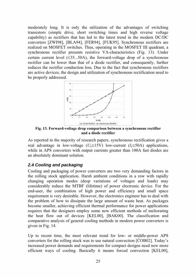
In the three-phase inverter each transistor has a maximum conduction period of 1200 (switching sequence for a three-phase inverter is depicted in Fig. 19). It means a maximum duty cycle D of each switch in the FBTP topology is 33.3%. In the conditions of the rolling stock, low-voltage power supply must provide stable output voltage at a rated load in the full range of input voltage (catenary) fluctuations (zero-percent line regulation). In practice it means that three-phase isolation transformer must be specified to provide maximal current just with the minimal input voltage (i.e.. 420...450V). Apparently, the most demanding operation conditions to the inverter switches are at the maximum input voltage (i.e., 720V) and rated load, when the duty cycle D becomes less than 1/3 of the full period. In this case, either one transistor switch and two freewheeling diodes or two transistor switches will be conducting at any time. Further, if the duty cycle is less than 1/6 of the full period, only one switch will turn on at a time and the output voltage from the converter will be zero. Thus, the required range of the duty cycle of any switch in three-phase inverter is
%3.33%7.16 ≤≤ D . (1)
31
90 180 270 360 ωt
90 180 270 360 ωt
90 180 270 360 ωt
90 180 270 360 ωt
90 180 270 360 ωt
90 180 270 360 ωt
90 180 270 360 ωt
90 180 270 360 ωt
∆ILo
ILo
S
T4
T5
T2
T3
T6
T1
T1 T4
T1 D3 D5
T1 T6
T6 D2 D4
T6 T3
a)
b)
c)
d)
e)
f)
g)
h)
1
1
1
1
1
1
1
Fig. 19. Theoretical waveforms of a three-phase inverter:
(a)…(f) transistors’ gating signals; (g) overall switching function S(ωt); (h) current waveform IO(ωt ) through the output filter inductor
a) b)
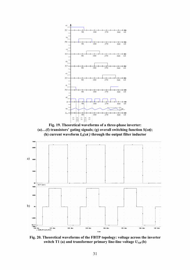
Fig. 20. Theoretical waveforms of the FBTP topology: voltage across the inverter
switch T1 (a) and transformer primary line-line voltage UAB (b)

32
a) b)
Fig. 21. Theoretical waveforms of the FBTP topology: isolation transformer’s
secondary line-line voltage Uab (a) and line current Ia (b)
3.2 Comparative analysis of FBTP and FBSP DC/DC converter topologies This section describes the steady-state analysis of the proposed FBTP topology. To simplify the analysis, the per unit (p.u.) system was used. The following comparison with the FBSP topology is mostly oriented on the evaluation of the new proposed topology. The recent and most widespread full-bridge single-phase isolated DC/DC converter topology will be analyzed in terms of similar assumptions and the selected criteria. The converter topologies will be analyzed under the following assumptions:
1. IGBTs are ideal, and the forward voltage drop and reverse leakage currents of feedback diodes are negligible;
2. forward voltage drop and reverse leakage currents of rectifier diodes are negligible;
3. filter components are ideal (no power dissipation); 4. the input DC voltage Uin of the converter is ripple free; 5. the high-frequency isolation transformers’ turn ratio is 1:1; 6. primary and secondary windings of isolation transformers are “wye”-
connected; 7. minimum input DC voltage Uin(min) = 1.0 p.u.; 8. maximum input DC voltage Uin(max) = 1.6 p.u.(possible catenary voltage
fluctuations 450...720VDC considered here); 9. rated output power of converter Pout = 1.0 p.u.
33
3.2.1 Output filter design
FBTP topology
In order to derive the necessary expressions required for the converter output filter design, the frequency spectrum of the input and output quantities Iin(ωt) and Io(ωt) must be known. These quantities can be easily obtained when the switching functions of the inverter and rectifier stages are represented in an overall switching function S(ωt). Moreover, the equivalent leakage inductances of the isolation transformer and/or any small external intermediate AC-link line inductances LA, LB and LC are much smaller than inductance of the output filter inductor Lo, and have a negligible effect on the output filter inductor current ILo. The representation of the overall switching function under maximum input DC voltage (Uin=1.6 p.u.) and rated load is shown in Fig. 19 (g). As the inverter input voltage decreases, the time between the pulses of S(ωt) decreases at the rated load. At the minimum input voltage (Uin=1.0 p.u), the overall switching function becomes constant. Although the overall switching function shown in Fig. 19 helps to visualize how the converter operates, it is also necessary to express it in the mathematical form in order to be able to obtain the required frequency spectra of the converter input and output currents Ii (ωt) and Io (ωt). Such a mathematical form can be obtained by deriving the Fourier series expansion given by
tnAAtSn
no ωω ∑∞
=
+=...12,6
sin)( , (2)
where An is the amplitude of the n-th harmonic component of S(ωt) and ω is the inverter’s operating frequency (taken as 1.0 p.u.).
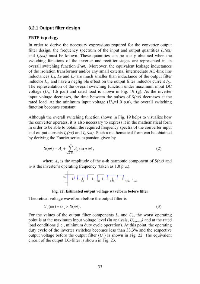
90 180 270 360 ωtU0
Fig. 22. Estimated output voltage waveform before filter
Theoretical voltage waveform before the output filter is
)()( tSUtU ino ωω ×= . (3)
For the values of the output filter components Lo and Co, the worst operating point is at the maximum input voltage level (in analysis, Uin(max)) and at the rated load conditions (i.e., minimum duty cycle operation). At this point, the operating duty cycle of the inverter switches becomes less than 33.3% and the respective output voltage before the output filter (Uo) is shown in Fig. 22. The equivalent circuit of the output LC-filter is shown in Fig. 23.

34
Uo Co
Lo
ZL
iLO(t)uL(t)
ILuLO(t)
iCO(t)
+ -
Fig. 23. Equivalent circuit of the output filter
Actual voltage waveform on the load terminals always contains two separate components: DC component (Udc) and AC component (ripple, uripple(t)) and can be characterized by the following equation:
)()( tuUtu rippledcL += (4)
By ignoring the ripple, the load voltage waveform can be easily determined as
dcripple Uu << , and (5)
dcL Utu ≈)( . (6)
For the simplification of further discussions voltage on the load terminals will be referred to as UL and with the minimum input DC voltage level will be equal to the voltage value before the filter Uo. Based on the steady-state analysis, output filter inductor voltage uLo(t) will be
)()( tuUtu LoLo −= (7)
With a small ripple approximation (see Eqs. (5) and (6)):
LoLo UUtu −=)( (8)
With the defined output inductor value, inductor current may be estimated as
dttdiLtu Lo
oLo
)()( ×= , and (9)
o
Lo
o
LoLo
LUU
Ltu
dttdi −
≈=)()( . (10)
The theoretical waveform of the inductor current ILo of the output filter is shown in Fig. 19 (h). It follows that in the worst operating point (at maximum input voltage level, Uin(max)=1.6 p.u. and at the rated load conditions (i.e., minimum duty cycle operation)), the approximated value of the peak-to-peak ripple current is given by
max),(max),(0.16.1
Uinpwo
Uinpwo
LoLo t
Lt
LUUI ×
−=×
−=∆ , (11)
where tpw(Uin, max) is the pulse width at the maximum input voltage.
35
Pulse width at the maximum input voltage may be determined as
swswsw
in
inUinpw TTT
UU
t ×=×=×=6625.0
66.11
6(max)
(min)max),( , (12)
where Tsw is the operating time period of the inverter (taken as 1.0 p.u.). From Eq. (11) and for the maximum input voltage (D=1/6Tsw), it follows:
o
swsw
oLo L
TTL
I ×=××=∆ 0625.06625.06.0 . (13)
Finally, the value of an output filter inductor is
Lo
swo I
TL∆
×= 0625.0 . (14)
The relation defining the capacitor of the output filter is
dttduCti Co
oCo
)()( ×= , and (15)
dttdu
tiCCo
Coo ×=
)()(
(16)
In well-designed converters, peak-to-peak current ripple and voltage ripple across the output filter capacitor can be assumed as 10% and 0.01%, respectively [MOH03]. In the FBTP topology, the dominant harmonic ripple current is six times the inverter operation frequency (Fig. 19, h). Thus, based on the above assumptions and considering the operating time period of the inverter Tsw=1.0 p.u., value of the filter capacitor will be given by
7.166)0.10001.0(6
1.0=
××=oC p.u. (17)
FBSP topology
In the single-phase topology the duty cycle of the inverter switches at the minimum input voltage Uin(min) and rated load is about 50% [PRA88]. At the maximum level of the input voltage Uin(max) the duty cycle of the switch becomes 35.7%. The overall switching function of the inverter and the rectifier S1(ωt) at the maximum input voltage Uin(max) is shown in Fig. 24 (b). Theoretical waveform of the output voltage Uo before the filter as well as the output filter’s inductor current ILo are shown in Fig. 24 (a) and (c). Further, filter inductor Lo and capacitor Co values will be estimated using the procedure of output filter analysis similar to the three-phase full-bridge topology (the same assumptions like maximum acceptable input voltage level, Uin(max)=1.6 p.u. and rated load conditions (i.e., minimum duty cycle operation)).

36
90 180 270 360 ωt
90 180 270 360 ωt
∆ILo
ILo
S1
UO
T1 T4 T2 T3
a)
b)
c)
90 180 270 360 ωt
1
Fig. 24. FBSP converter waveforms:
(a) - output voltage before filter; (b) - overall switching function S(ωt); (c) - current IO(ωt ) through the output filter inductor
Pulse width at the maximum input voltage in the FBSP topology may be determined as
swsw
Uinpw TTt ×=×=2625.0
26.11
max),( . (18)
The value of the output filter’s inductor Lo in the FBSP topology will be
Lo
swo I
TL∆
×= 1875.0 . (19)
In well-designed converters, peak-to-peak current ripple and voltage ripple across the output filter capacitor can be assumed as 10% and 0.01%, respectively [MOH03]. In the FBSP topology, the dominant harmonic ripple current is two times the inverter operation frequency (Fig. 24, c). Thus, based in the above assumptions and considering the operating time period of the inverter Tsw=1.0 p.u., value of the filter capacitor Co will be given by
0.500)0.10001.0(2
1.0=
××=oC p.u. (20)
3.2.2 Inverter switch ratings
FBTP topology
The duty cycle of the three-phase inverter transistors at the rated load and minimum input voltage level will be 0.333 (33.3%). The peak value of the square current pulses through the inverter switches at the minimum supply voltage:
(min))(
in
outpeaksw U
PI = = 1.0 p.u. (21)
Average current through the respective inverter switch:
∫ ×=333.0
0)()( dtII peakswavsw = 0.333 p.u. (22)
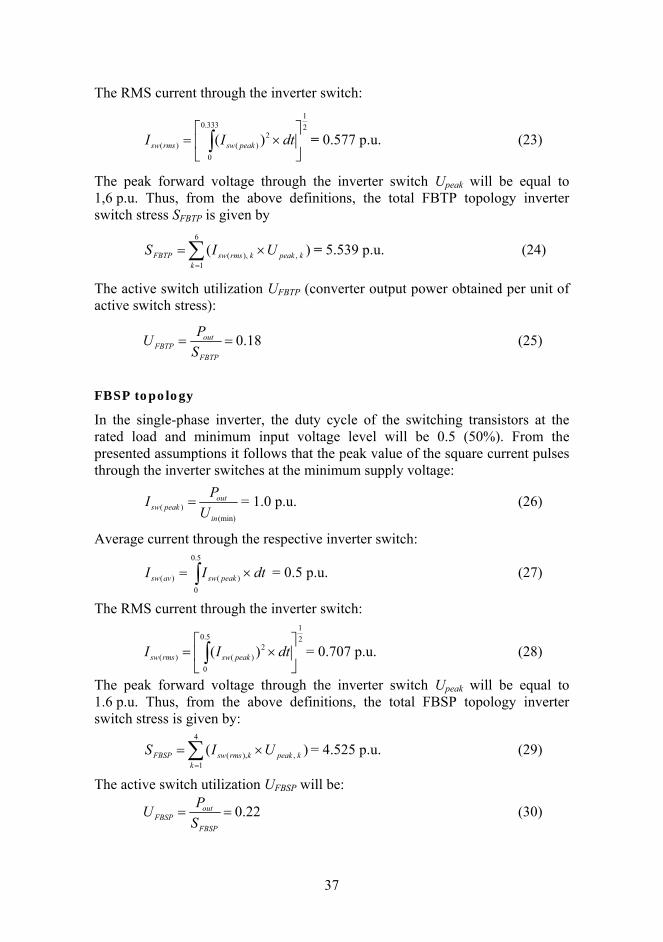
37
The RMS current through the inverter switch:
21
333.0
0
2)()( )( ⎥
⎦
⎤⎢⎣
⎡×= ∫ dtII peakswrmssw = 0.577 p.u. (23)
The peak forward voltage through the inverter switch Upeak will be equal to 1,6 p.u. Thus, from the above definitions, the total FBTP topology inverter switch stress SFBTP is given by
∑=
×=6
1,),( )(
kkpeakkrmsswFBTP UIS = 5.539 p.u. (24)
The active switch utilization UFBTP (converter output power obtained per unit of active switch stress):
18.0==FBTP
outFBTP S
PU (25)
FBSP topology
In the single-phase inverter, the duty cycle of the switching transistors at the rated load and minimum input voltage level will be 0.5 (50%). From the presented assumptions it follows that the peak value of the square current pulses through the inverter switches at the minimum supply voltage:
(min))(
in
outpeaksw U
PI = = 1.0 p.u. (26)
Average current through the respective inverter switch:
∫ ×=5.0
0)()( dtII peakswavsw = 0.5 p.u. (27)
The RMS current through the inverter switch:
21
5.0
0
2)()( )( ⎥
⎦
⎤⎢⎣
⎡×= ∫ dtII peakswrmssw = 0.707 p.u. (28)
The peak forward voltage through the inverter switch Upeak will be equal to 1.6 p.u. Thus, from the above definitions, the total FBSP topology inverter switch stress is given by:
∑=
×=4
1,),( )(
kkpeakkrmsswFBSP UIS = 4.525 p.u. (29)
The active switch utilization UFBSP will be:
22.0==FBSP
outFBSP S
PU (30)

38
3.2.3 Rectifier diode ratings In the analysis, the two most widespread single-phase rectifier topologies for the FBSP converter (center-tap (M2U) and the two-pulse bridge (B2U)) were compared with the three-phase six-pulse bridge rectifier (B6U), which is obviously the optimal choice for the secondary side rectifier for the FBTP topology. Fig. 25 shows the theoretical voltage Uo and current Io waveforms of the discussed topologies.
1)
2)
1)
2)
)
(a) (b)
Fig. 25. Theoretical voltage (1) and current (2) waveforms before the output filter of the M2U, B2U rectifiers (a) and B6U rectifier (b)
On analogy with the calculation of inverter switch ratings, the ratings of the output rectifier diodes can be analyzed for both FBTP and FBSP topologies. Let us assume that the losses in the rectifier assembly are negligible. The maximal ratings of the different rectifier topologies (applicable to the resistive load) are presented in Table 5. Table 5. Evaluative analysis of different diode rectifier topologies
Compared topology FBTP topology FBSP topology
Rectifier’s option Six-pulse bridge rectifier
Center-tap rectifier
Two-pulse bridge rectifier
Number of diodes 6 2 4
Ripple frequency in relation to the operating frequency 6 2 2
Average diode current 0.333 0.5 0.5
Transformer utilization factor (TUF) 0.95 0.57 0.81
3.3 Validation of predicted results by Spice modeling In order to validate assumptions predicted in the analysis, the FBTP and FBSP DC/DC converter topologies will be compared by help of the PSpice simulation tool. The values of an output LC-filter components (capacitors and inductors) are calculated in accordance with the specific requirements presented in Table 6.
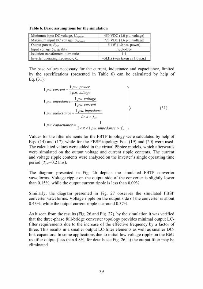
39
Table 6. Basic assumptions for the simulation
Minimum input DC voltage, Uin(min) 450 VDC (1.0 p.u. voltage) Maximum input DC voltage, Uin(max) 720 VDC (1.6 p.u. voltage) Output power, Pout 5 kW (1.0 p.u. power) Input voltage Uin quality ripple-free Isolation transformers’ turn ratio 1:1 Inverter operating frequency, fsw ~5kHz (was taken as 1.0 p.u.)
The base values necessary for the current, inductance and capacitance, limited by the specifications (presented in Table 6) can be calculated by help of Eq. (31).
voltageuppowerupcurrentup
..1..1..1 =
currentupvoltageupimpedanceup
..1
..1..1 =
swfimpedanceupancetinducup
××=
π2..1..1
swfimpedanceupancecapacitup
×××=
..121..1
π
Values for the filter elements for the FBTP topology were calculated by help of Eqs. (14) and (17), while for the FBSP topology Eqs. (19) and (20) were used. The calculated values were added in the virtual PSpice models, which afterwards were simulated on the output voltage and current ripple contents. The current and voltage ripple contents were analyzed on the inverter’s single operating time period (Tsw=0.21ms). The diagram presented in Fig. 26 depicts the simulated FBTP converter vaweforms. Voltage ripple on the output side of the converter is slightly lower than 0.15%, while the output current ripple is less than 0.09%. Similarly, the diagram presented in Fig. 27 observes the simulated FBSP converter vaweforms. Voltage ripple on the output side of the converter is about 0.43%, while the output current ripple is around 0.37%. As it seen from the results (Fig. 26 and Fig. 27), by the simulation it was verified that the three-phase full-bridge converter topology provides minimal output LC-filter requirements due to the increase of the effective frequency by a factor of three. This results in a smaller output LC-filter elements as well as smaller DC-link capacitors. In some applications due to initial low voltage ripple on the B6U rectifier output (less than 4.8%, for details see Fig. 26, a) the output filter may be eliminated.
(31)
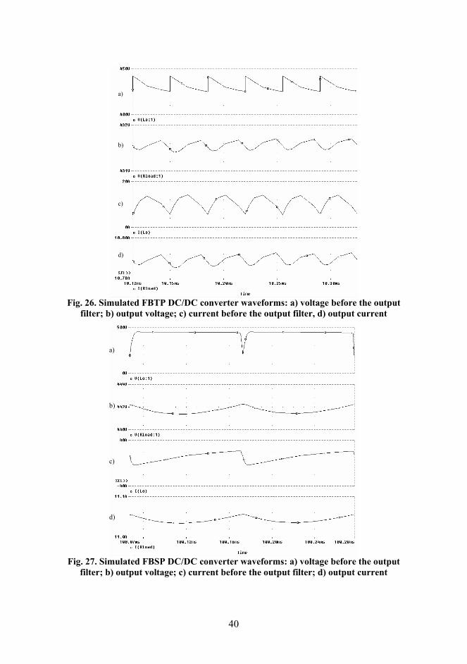
40
a) b) c) d)
Fig. 26. Simulated FBTP DC/DC converter waveforms: a) voltage before the output
filter; b) output voltage; c) current before the output filter, d) output current a) b) c) d)
Fig. 27. Simulated FBSP DC/DC converter waveforms: a) voltage before the output
filter; b) output voltage; c) current before the output filter; d) output current

41
3.4 Final evaluation of the proposed topology Basic key points following from the FBTP and FBSP converter analysis are submitted in Table 7, while specific advantages are designated in Bold Italics. Table 7. Side-by-side comparison of FBTP and FBSP converter topologies
Proposed FBTP topology FBSP topology Inverter switch ratings:
RMS current Average current
0.577 p.u. 0.333 p.u.
0.707 p.u. 0.500 p.u
Active inverter switch utilization 0.18 0.22 Rectifier diode ratings:
Average current TUF
0.333 p.u.
0.95
0.500 p.u. 0.57/0.81
Output ripple frequency in relation to the operating frequency 6 2
Output filter components: capacitor
inductor
166.7 p.u.
0.0625⎟⎟⎠
⎞⎜⎜⎝
⎛
∆ Lo
sw
IT
500.0 p.u.
0.1875 ⎟⎟⎠
⎞⎜⎜⎝
⎛
∆ Lo
sw
IT
The bottom line is that the full-bridge three-phase topology in comparison with the full-bridge single-phase topology (for the same transferred power) exhibits the following advantages:
1. Lower inverter switches ratings: average inverter switch current is 1.5 times lower as compared with the FBSP topology. It directly influences the minimization of total power switch losses (e.g., minimization of steady-state losses of IGBT and free-wheeling diode) and means smaller devices to be used.
2. Lower rectifier diode ratings: average diode current is 1.5 times lower as compared to different FBSP topology rectifier options. It directly influences the minimization of total power switch losses (e.g., minimization of per-diode conduction losses I2R) and means smaller devices to be used.
3. Lower output filter components ratings: FBTP topology output (smoothing) filter components values are more than 60% lower in comparison with the FBSP topology for the same transferred power. As the minimization of the magnetic component sizes is the one of the basic trends in modern power electronics, this advantage of the FBTP topology becomes very important. Moreover, due to the potential lowering of the output smoothing filter, the response bandwidth of the three-phase DC/DC topology can be made much wider.
4. Three-phase transformer requires less magnetic core material. It means lower weight and size as compared to a single-phase transformer. As the isolation transformer is the main contributor to the size of any switching-mode power supply since it contributes about 25…30% of the
42
overall volume and more than 30% of the overall weight, such advantage of the FBTP topology helps to develop compact converters with high power densities. The transformer utilization factor (TUF=PDC/UsIs) is 0.95 for the three-phase full-bridge rectifiers [RAB90]; but only 0.57 and 0.81 for a center-tap and full-bridge single-phase rectifiers, correspondingly.
5. The dominant harmonic ripple frequency of the input DC current is three times the dominant harmonic ripple frequency of the input DC current of the single-phase topology that means smaller input filters and finally lowers impact on the supply grid.
6. The possibility to use a three-phase transformer with different interconnections (e.g., Y- or ∆ - connections) in its primary and secondary windings gives a potential freedom and flexibility in choosing the voltages and currents in the inverter, transformer and rectifier. As a result, it is possible to lighten the operation conditions of inverter switches and rectifying diodes.
From the opposite (negative) point of view, the increased quantity of inverter switches of three-phase topology (from 4 to 6) despite lower RMS current of each switch tends to increase approx. 18% of the total inverter switch stress (reduced switch utilization ratio). The same assumption is connected to the rectifier diodes as well.

43
4. Design, Implementation and Evaluation of a New APS for the LRV To verify the theoretically predicted assumptions and results and to validate the proposed FBTP topology, an experimental APS converter has been designed and implemented by the author on the tram KT4 (ČKD).
4.1 Design overview Power scheme design of the developed prototype is presented in Fig. 28. The catenary voltage is passed to the three-phase high-frequency inverter (3) via EMI filter (1) and input LC-filter. The charging circuit (soft-start) prevents a starting current inrush under all possible operating conditions (e.g., full-load operation during catenary sags). Three-phase high frequency “step-down” transformation system (4) with the 10 kHz frequency of the main harmonic is responsible for the converter I/O galvanic isolation. Transformers are “wye-wye” connected, which is most economical for compact, high-voltage transformers because the number of turns/phase and the amount of insulation is minimal. Voltage rectification is performed in the non-controlled high frequency rectifier (5). The output (smoothing) filter is minimal because of initially low voltage ripple on the rectifier output, which is a great advantage of the proposed three-phase DC/DC converter topology. As it seen from the Fig. 28, the developed system is additionally equipped with an auxiliary inverter (9) for the producing AC power for the blowers of traction motors (was implemented on the end-user demand). All the output parameters of the APS are precisely controlled by the control system (7), which has an advanced “black-box” function for the error log.
R1
R2
R3
R4SH1
TX2
TX3
C1
L1
D1
RU1
Softstart
EM
I - F
ILTE
R
C3
C2
L2
C4
C5
IGBT-Driver 2
VD
T1 T5T3D2
T6T2 T4
D4
D3 D5
D6
D7
DM1
DM4
RU2
IOUT (output current)
VOUT (output voltage)
VIN
(inpu
t vo
ltage
)
HF INVERTER 13-PHASE HF TRANSFORMATION
SYSTEM ( ) HF RECTIFIER
+
+
+
400...800 VDC
27 VDC
TX1
DM2
DM3 DM5
DM6
C21R21
R22
L21
D21
C22
T21 T25T23D22
T26T22 T24
D24
D23 D25
D26
D27
INVERTER 2
+
+
U BAT (onboard battery voltage monitoring)
IBAT (onboard battery charging current, available as option )
IGBT-Driver 2
VD
RS232
3x400 VAC
Ia Ib Ic
CONTROL SYSTEM
13 4 5
9
8
6
7
2
ASI
Fig. 28. Power circuit design of the developed APS

44
4.1.1 Novelties implemented in hardware design Low stray inductance laminated busbars
In hard-switched high-frequency inverters special attention need to be attached to interconnections of components to minimize the distributed inductances. Therefore the circuit wiring inductance to the transistor modules can cause high switch-off surge voltages (Fig. 30, a). The IGBT switch-off surge voltage UCES can be estimated as follows:
)(dt
dILUU CSDCCES ×−+= , (32)
where UDC is the inverter DC-link voltage, LS - commutation loop stray inductance, dIC/dt – maximum IGBT collector current change rate at switch-off. If UCES exceeds the IGBT’s collector-emitter voltage rating (UCE), the transistor module can be destroyed. Hence, in terms of reducing UCES it is important to reduce all the inductance components which contribute to the total stray inductance Ls of the commutation loop:
IGBTscrewsCwirS LLLLL +++= . , (33)
where Lwir. - interconnection wiring inductance, Lscrews - stray inductance caused by mechanical contacts, LC - self-inductance of DC-link capacitors and LIGBT - internal stray inductance of IGBT module. While Lc and LIGBT are fixed parameters, Lwir can be sufficiently reduced by means of laminated copper busbars and short current leads between the DC-link and the power devices. Width and thickness of plates are determined by the specified electrical requirements, taking into consideration rigidity and the number of mounting holes required. For this case study, the mechanical dimensions of the bus bar are: length 145 mm, width 185 mm and thickness 1.5 mm (Fig. 29, a). By the PSpice modeling of the commutation loop (UDC=600V and IC=25A), the proposed planar busbar design reduces the IGBT switch-off surge voltage almost twice (Fig. 30).
VARISTOR
SNUBBER CAPACITOR
NEGATIVE (-) BUSBAR
a) b) Fig. 29. Proposed design of the inverter: a) (+) busbar on the APS inverter bridge,
b) final layout of inverter in the developed APS

45
Ic=25A
Uces=748V
100V/div 0.1us/div
Ic=25A
Uces=700V
100V/div 0.1us/div
(a) (b)
Fig. 30. Simulated switch-off overvoltages across one IBGT: (a) with standard wiring (commutation loop stray inductance 300 nH); (b) with proposed laminated
busbars (commutation loop stray inductance 170nH)
High-frequency three-phase Power Schottky rectifier
The developed high-frequency DC/DC converter inevitably sees more than 250A on the secondary side with the voltage of 24...28 VDC, making the design of the output rectifier stage very challenging. To accomplish the project, advanced High Power Schottky diodes were chosen. From the author’s point of view, the combination of “very fast-soft switching” properties of Schottky diodes can eliminate the need for additional snubber circuits in many applications that may otherwise be required with fast or ultrafast rectifiers displaying abrupt recovery characteristics. But some troubles were caused by the limited mean forward current (IF(AV)) value of the Schottky devices (about 80-100A).
A
B
C
–
–
+
+
+
–
Dual-Pack diode modules
Phase (AC) inputs
Rectifier (DC) outputs Phase inputs Rectifier (-) output
(a) (b)
Fig. 31. Proposed design of the rectifier stage in the developed converter: (a) methodology of interconnection, (b) general view

46
As the preferred devices (STPS160H100TV from ST Microelectronics) are dual-packaged in ISOTOPTM cases, to increase the output current capability of the converter it was decided to connect dual diodes in parallel by help of special designed multilayer laminated copper busbars1 (Fig. 31). With such a combination, a mean forward current capability of 160A per device and excellent compactness and cooling of the three-phase rectifier were achieved.
Compact design of power assembly/cooling
To realize the compact APS, the advanced hollow-fin cooling aggregate with an airflow chamber LAV 17/300/24 from FISCHER ELEKTRONIK was chosen. The aggregate was equipped with an axial DC cooling fan. The thermal resistance of the chosen aggregate with 24 VDC fan is 0.047K/W, which was in agreement with the performed predictive loss analysis. Fig. 32 demonstrates the proposed arrangement of power devices on the back and top sides of the cooling aggregate1, including the IGBT modules of the DC/AC inverter with an external driver, Schottky diode modules and reverse polarity protection diodes as well as DC-link capacitors and input filters’ inductors of both converters. On the front mounting plane of the heatsink, the IGBT modules of the DC/DC converter with an external driver as well as the current limiting resistor of the soft-start system were fitted. The volume of the proposed power stack is only 0.012 m3, which is an excellent result compared with other similar devices.
DC-Link Capacitors
Input Diode (2)
3-Phase IGBT Bridge (2) IGBT Driver (2) 3-Phase Power Schottky Rectifier
Input Choke (2)
Cooling aggregate with a 24VDC
axial fan
Fig. 32. Proposed arrangement of power devices on the cooling aggregate LAV17
1 Was described by the author in the registered Estonian Utility Model (Certificate EE00331U1).

47
Compact power module Transformers’ assemblyFig. 33. Front view of power assembly of the developed APS
4.1.2 Proposed control method of the high-frequency inverter To achieve a good line/load regulation with a very wide tolerance of an input voltage (Uin= -30%, +20%), isolation transformers were specified to produce the maximal load current just at the minimal primary voltage. Considering the wide variety of loads at any operation time of the converter, the inverter stage must be carefully controlled to achieve a good overall efficiency and flexibility of the APS. From the numerous methods of PWM strategies [BRO88], [BUS92], [POL86], [ZIO90], a simplified SVPWM was introduced. The proposed method uses only switching between the base and zero vectors, thus achieving a better DC-link voltage utilization (by 15% in comparison with the conventional SVPWM,
32 DCU and
3DCU , respectively) and a reduced number of switching
actions. Actually, this control method is the only valuable way for providing 10 kHz AC-voltage for the feeding of isolation transformers, which may fully utilize the processor’s resources and IGBT switching capabilities. The idea of the implemented method is that the projected isolation transformer’s primary winding voltage vector Upri , at any given time, falls into one of the six base vectors. Thus, for any PWM period it may be approximated as
)( 1110000 OorO
TtU
TtU
pwmx
pwm
kpri ×+×= , (34)
where Ux is one of the six base vectors, t0= Tpwm - tk and Tpwm is the PWM carrier period. Duty ratios of active and zero states (ak and a0, respectively):
pwm
kk T
ta = and
pwmTta 0
0 = , (35)
while the sum of these duty ratios will always be: ak + a0 = 1.

48
By adjusting the duty ratios of the active and zero states (Fig. 34) the desired output voltage can be applied to the transformers’ primary winding 2(Fig. 35).
0 0.5 1 1.5 2 2.5 3 3.5 4
x 10-4
-0.5
0
0.5
1
1.5T1 Gating Signal (10%)
(a)
0 0.5 1 1.5 2 2.5 3 3.5 4
x 10-4
-0.5
0
0.5
1
1.5T1 Gating Signal (100%)
(b)
Fig. 34. Matlab-simulated gating signals: (a) voltage vector magnitude 10%; (b) voltage vector magnitude 100%
1) Ref B: 155 Volt 2.5us
1 >
Fig. 35. Measured voltage waveform (isolation transformer primary line-line
voltage, with voltage vector magnitude 80%)
2 Proposed control method was described by the author in the registered Estonian Utility Model (Certificate EE00331U1)

49
4.1.3 Generalized mathematical model of the developed system To investigate the developed system, a generalized mathematical model was developed with the help of Matlab-Simulink program (Fig. 36).
Fig. 36. Generalized mathematical model of the developed DC/DC converter
Simulations were performed with the following parameters:
• solver option: Fixed-Step, oder 4 (Runge-Kutta), • sample time: 200 ns, • simulation time: 2...6 ms, • PWM carrier frequency: 10 kHz, • desirable load: ZL=0.54...0.1Ω (for IL= 50...270A with constant output
voltage level UL=26.7 VDC), • possible catenary supply Uin: 420...800 VDC.
Some waveforms mainly concerning the operation of the investigated DC/DC converter at low catenary voltage level (Uin=500 VDC) and maximal possible load (e.g., electromagnetic brakes, IL=270A) are depicted in Fig. 37, Fig. 38 and Fig. 39. A detailed analysis of the simulated waveforms showed that with the proposed power scheme topology and control strategy, as well as with the selected values of filtering elements, the output current and output voltage ripple will not exceed 2% and 1%, correspondingly.

50
0.4 0.6 0.8 1 1.2 1.4 1.6 1.8 2
x 10-3
-2
0
2
4Switch T1 gating signals
0.4 0.6 0.8 1 1.2 1.4 1.6 1.8 2
x 10-3
0
200
400
600
800Phase A top switch (T1) voltage
0.4 0.6 0.8 1 1.2 1.4 1.6 1.8 2
x 10-3
-20
0
20
40Phase A top switch (T1) current
Fig. 37. Simulated transistor voltage and current waveforms
0.4 0.6 0.8 1 1.2 1.4 1.6 1.8 2
x 10-3
-300
-200
-100
0
100
200
300Transformer secondary current
0.4 0.6 0.8 1 1.2 1.4 1.6 1.8 2
x 10-3
-60
-40
-20
0
20
40
60Transformer output voltage
Fig. 38. Simulated transformer’s secondary voltage and current waveforms

51
0 0.5 1 1.5 2 2.5 3 3.5 4
x 10-3
240
250
260
270Output filter inductor current, ILo
0 0.5 1 1.5 2 2.5 3 3.5 4
x 10-3
0
100
200
300Converter output current, Iout
0 0.5 1 1.5 2 2.5 3 3.5 4 -50
10
20
30Converter output voltage, Uout
Fig. 39. Secondary-side voltage and current waveforms of the converter
4.2 Evaluative analysis of the developed system
4.2.1 Efficiency analysis APS converter losses are generated in passive (resistors, capacitors, inductors, transformers, etc.) and active components (transistors, diodes, etc.). Losses in passive components are usually small compared with others. Thus, the losses in the switching elements are decisive.
The efficiency of the developed converter may be estimated by the following equation:
inin
k
xxxinin
IU
apIU
×
−×=
∑=1
)(η , (36)
where Uin is an input voltage value, Iin is an input current, px is the power loss of the device x and ax is device’s x relative on-state time (a=0...1). Step-by-step calculation of losses of the developed FBTP converter was performed for different operation modes. The efficiency of the converter at the nominal mode (nominal input voltage, Uin=600VDC, output current IL=160ADC) was 90%, which is quite a good result for such devices with high-frequency hard-switching. The breakdown of losses is presented in Fig. 40.
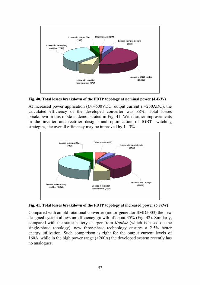
52
Losses in output filter (19W)
Losses in isolation transformers (37W)
Losses in input circuits (22W)
Other losses (12W)
Losses in secondary rectifier (174W)
Losses in IGBT bridge (234 W)
Fig. 40. Total losses breakdown of the FBTP topology at nominal power (4.4kW)
At increased power application (Uin=600VDC, output current IL=250ADC), the calculated efficiency of the developed converter was 88%. Total losses breakdown in this mode is demonstrated in Fig. 41. With further improvements in the inverter and rectifier designs and optimization of IGBT switching strategies, the overall efficiency may be improved by 1...3%.
Losses in IGBT bridge (268W)Losses in secondary
rectifier (319W)
Other losses (48W)Losses in input circuits
(34W)
Losses in isolation transformers (71W)
Losses in output filter (79W)
Fig. 41. Total losses breakdown of the FBTP topology at increased power (6.8kW)
Compared with an old rotational converter (motor-generator SMD5003) the new designed system allows an efficiency growth of about 35% (Fig. 42). Similarly, compared with the static battery charger from Končar (which is based on the single-phase topology), new three-phase technology ensures a 2.5% better energy utilization. Such comparison is right for the output current levels of 160A, while in the high power range (>200A) the developed system recently has no analogues.

53
54
9087.5
0
10
20
30
40
50
60
70
80
90
100
Motor-GeneratorSMD5003
Koncar BatteryCharger
APS TSM1
Ove
rall
effic
ienc
y, %
UL=27 VDC, IL=160A
Fig. 42. Compared efficiencies of different APS types
4.2.2 Performance tests The first prototype of the auxiliary power converter TSM1 was built by the author and his colleagues at the Department of Electrical Drives and Power Electronics of TUT in 2002. The developed converter has been thoroughly tested in the laboratory, depot and traffic conditions on all Tallinn tram routes. During the testing period some hardware implementations as well as control and protection algorithms were optimized and tuned. All functionality tests were performed in accordance with the European Norm EN 50155:2001 (Railway applications - Electronic equipment used on rolling stock). Fig. 43 shows the load regulation possibilities during the changing operation conditions of a vehicle: the output current despite the deep fluctuations (starting-moving-braking a tram) has no influence on the output voltage, which was perfectly regulated on the level of 26 VDC.
0
25
50
75
100
125
150
1 501 1001 1501 2001 2501 3001 3501 4001 4501 5001 5501 6001t (x5), s
Iout, A
0
25
50
75
100
125
150
Uout, V
Output current, I out
Output voltage, U out
Fig. 43. Demonstration of the load regulation of the APS TSM1

54
In case of the load transient response measurements (Fig. 44), the developed prototype showed the transient recovery times tr(-) and tr(+) no longer than 0.7 s, which is in the full agreement with the Standard IEEE Std. 1476-2000 (required at least 1 s). The momentary voltage drop in the case of 2.3 p.u. overload (electromagnetic brakes are applied) did not exceed 0.5 VDC (1.9%). The secondary low-voltage DC supply system voltages overshoot after the switching-off the load did not exceed 1 VDC (4%, compared with 20% required by the Standard).
0
25
50
75
100
125
150
175
200
225
250
1 11 21 31 41 51 61 71 81 91 101 111 121
t, s
Iout, A
20
21
22
23
24
25
26
27
28
29
30
Uout, V
Output current, I out
Output voltage, U out
Fig. 44. Demonstration of the load transient response of the APS TSM1
200
260
320
380
440
500
560
620
680
740
800
1 501 1001 1501 2001 2501 3001 3501 4001 4501 5001 5501 6001
t (x2), s
Uin, V
18
20
22
24
26
28
30
32
34
36
38
Uout, V
Input (catenary) voltage, U in
Output voltage, U out
Fig. 45. Demonstration of the line regulation of the APS TSM1
The investigated line regulation capability of the developed prototype is demonstrated in Fig. 45. Despite the deep voltage fluctuations on the primary

55
side of the converter (catenary voltage sags), the output voltage was absolutely stable and within the specified limits. Based on the experimental and theoretical background, the main specifications of the developed converter TSM1 were specified, shown in Table 8. Table 8. Technical specifications of the developed APS
MAIN PURPOSE Feeding of LRV onboard low-voltage systems and devices, charging of onboard back-up battery, feeding of cooling blowers for traction motors, feeding of air conditioners
MAIN TECHNICAL DATA Input voltage range 600 VDC (+33%, -33%)
according to EN50163 Number of output sections 2
PARAMETERS OF THE DC OUTPUT SECTION Output voltage 27 VDC (+3%, -3%) Output voltage ripple ≤2% Nominal current 160 A Peak current (15 s) 250 А Nominal/peak power 4.5/6.8 kW
PARAMETERS OF THE AC OUTPUT SECTION Output voltage (regulated) 3~0...400 VACrms , 5…60 Hz Nominal power 3...10 kVA (on demand)
SIGNALING Signaling is achieved through the relay output. All relevant information can be read and recorded via the RS232 interface
Max. load current of relay output 1 A Voltage supply 27 VDC
MISCELLANEOUS Cooling Forced convection Input/output voltage isolation 2 kV Ambient temperature -35 to +60 0C Relative humidity 15…100% Dimensions (W x D x H) 600 x 380 x 380 mm (excl. blowers) Weight approx. 60 kg (excl. blowers) Noise level < 65 dBA at a distance of 1m Protection class (casing) IP65Vibration resistance according to EN50155 EMC according to EN50121-3-2 MTBF > 65000 Hours

56
4.2.3 Final evaluation The developed dual-output auxiliary power supply system TSM1 represents the new generation of converters applied to feeding onboard consumers in the light rail vehicles. The use of advanced semiconductor technologies and robust mechanical design are connected to meet the demanding requirements of rail applications and to ensure a good performance and a high level of availability. Evaluative (SWOT) analysis of the developed system is given in Table 9. Table 9. SWOT-analysis of the developed system
System Factors Strengths • Compact, modular design
• Flexible control • High output power • Low DC output voltage ripple • Excellent line/load regulation • Excellent load transient response • Improved hardware/software
protection algorithms • Error logging for better and faster
maintenance and service organization
• Accepts using different onboard battery types (NiCd, Pb-Acid)
• Possibility of interconnection with the onboard automation network of the light rail vehicle (CAN)
• Low weight and noise • Low price • Defended by the Estonian Utility
Model Certificate Weaknesses • Relative complexity
• Requires more qualified service personnel
• Weak mechanical construction of casing and fixing elements
Opportunities • Easy to reconfigure • Easy to adapt to different LRV
types and light trains • Easy to adapt to trolleybuses • Easy to adapt for industrial
applications (welding aggregates, power supplies, telecommunication facilities, etc.)
Auxiliary power supply TSM1 for the Light Rail Vehicles (e.g., for trams KT4, KT6, T4)
Threats • Developed technology is patent-protected only in Estonia and very attractive for the European competitor companies

57
Table 10 provides an evaluative comparison of the developed APS system TSM1 (among the physical specifications and functional parameters of the APS channel) with some identical and recently widespread devices from European companies like VACON TRACTION (Finland), ENIKA (Poland), and KONČAR (Croatia). New developed converter definitely overcomes all the presented competitors in all the listed specifications. Table 10. Comparison of similar APS from different vendors
Fig. 46 demonstrates technological advancement in APS systems for the LRV, achieved by the development and implementation of a new full-bridge isolated DC/DC converter with a three-phase intermediate AC-link.
0.14 m3
0
0,04
0,08
0,12
0,16
Vacon Traction 5TX600
Enika ENI PT600/24/AC
New proposedsystem TSM1
Volu
me,
m3
0.12 m3 0.1 m3100 kg 90 kg 60 kg
90
120
60
30
0
Wei
ght,
kg
- Volume of the device
- Weight of the device Fig. 46. Comparison of systems among major end-user specifications
Vacon Traction, 5TX600 120(160)
DCDC600
Končar Company,
Battery Charger 150 A, 24 V
Enika, ENI-
PT600/24/AC
Tallinn University of Technology,
TSM1 Nominal output current, A 120 120 100 160
Peak output current, A 160 160 150 250
Nominal/peak output power, kW 3.2/4.5 3.2/4.5 2.7/4.0 4.5/6.8
Dimensions (LxWxH), mm 952x386x386 n.a. 790x360x422 600x380x380
Weight, kg 100 n.a. 90 60 General evaluation
Good, if the price is acceptable. Sometimes lack of output power in high power applications (electromagnetic brakes, IL,=230A)
Good, but the lack of power is limiting factor. Some problems with cooling are possible
Good, but the lack of power is limiting factor. Some problems with cooling are possible
Very good. Very flexible, many possibilities, very compact, high output current. With small improvements suitable for other tram/LRV types

58
5. Future Research and Development
5.1 Development of APS converter for the commuter trains The past five years has witnessed major advances in power electronics technology for both industrial and traction applications. These advances have made it possible to significantly improve the electrical performance of systems while simultaneously reducing their size and weight and, perhaps most importantly, reducing their cost. For instance, the lately developed and tested innovative 6.5kV IGBT modules (EUPEC, Infineon Group Ltd., [BAU01], [AUE99]) make it possible to adapt newly developed power converter topology to railway systems with 1.5 kVDC or even 3 kVDC overhead supply lines (Fig. 47).
GALVANICALY ISOLATED HIGH VOLTAGE INPUT UNIT
Isolated DC/DC voltage converter with a three-phase intermediate AC-link (based on the developed
concept), with high-voltage state-of-the-art IGBT transistors and fast recovery diodes Inverter with variable
frequency
Inverter with fixed frequency (50Hz)
DC/DC APS with 110VDC output
DC/DC APS with 110VDC output
OUTPUT MODULES (Quantity and specifications are dependable
on the application)
CATENARY 3000VDC±30%
ONBOARD CONSUMERS
Fig. 47. Proposed power circuit topology for the 3 kVDC converter
The specificity of the secondary low-voltage supply system of trains is that they need two different secondary DC-voltage buses and some auxiliary inverters. As a rule, DC buses are 50 VDC (5-10 kW, for supplying onboard systems like lighting, information and communication, as well as for charging the onboard back-up batteries) and 110 VDC (10-20 kW, for supplying electro-hydraulic braking system and other onboard HPDC systems). The converters, providing these voltages (so-called output modules) are separate units with independent control. Additional inverter units may be as follows: with a fixed or with a variable frequency, with total output power of some tens kW. It leads to 40-60 kW output power required from the primary DC/DC voltage input unit. With the implementation of the developed concept of an isolated DC/DC converter with a three-phase intermediate AC-link in the input stage of the APS system allows one to achieve very compact and efficient power scheme design. High available output current, low output voltage ripple, low stresses of the inverter switches and the rectifier diodes as well as other positive aspects of the developed technology will be a good alternative for the development of a compact and reliable APS for the locomotives and commuter passenger trains.
5.2 Use of ultracapacitors in LVPS systems of LRVs In the normal operation, an APS converter must ensure trouble-free operation of all the subsystems connected to it outputs. But in the case of crossing of catenary

59
section disconnectors, when the output voltage of the APS converter drops to zero, all the secondary low-voltage systems are supplied from the tram back-up battery. After the disconnector, battery is refilled from the APS. It means that the onboard battery needs to have sufficient energy density (to provide constant power to such loads, like lighting, announcement systems, etc.) and high power density (for peak current demands, like emergency braking). Namely, the last criteria have raised many questions in several European tram or LRV companies. Based on the huge amount of investigations, it has been stated that namely the back-up battery is the weakest part on old and even on new trams. For instance, in winter with low outside temperatures, the productivity of the accumulator battery dramatically decreases, because of increased internal resistance, which, in turn, depends on the electrolyte’s density. Further, with very low temperatures (-35 0C and lower), productivity is so low, that the battery even can not been charged. Finally it means that sometimes during section disconnectors and in the case of dangerous traffic situation, a tramcar driver is not able to stop the tram with the emergency (electromagnetic) brake because of the discharged back-up battery. Thus, rugged railway RAMS requirements are violated and it may cost sufficient penalties to the tramcar company. As an alternative to the accumulator battery in such demanding conditions and peak power requirements the author proposes to use ultracapasitors [MAX02] in the secondary low-voltage power supply bus (LVPS) of the LRV connected in parallel with the onboard back-up battery.
CONTINUOUS POWERDEMANDS(LIGHTING,
ANNOUNCEMENT, CONTROL SYSTEMS )
ULTRACAPACITOR
TRAM ONBOARD BACK-UP BATTERY
TRAM ONBOARD COMBINEDENERGY STORAGE SYSTEM
PEAK POWER DEMANDS(ELECTROMAGNETICBRAKES, AUXILIARY
DRIVES)
TRAM SECONDARYLOW-VOLTAGE SYSTEMS
TRAM AUXILIARY POWER SUPPLY (APS)
TRAM CATENARY (MAIN SUPPLY SYSTEM)
Power transfer during catenary supply
Power transfer during section disconnector
Fig. 48. Proposed scheme of a low-voltage secondary supply system
In the proposed scheme (Fig. 48), the peak power demands of the vehicle will be supplied from the ultracapacitor module (due to extremely low ESR), after which it will be refilled from the back-up battery. Thus, the overall size of a back-up battery may be sufficiently reduced, while the efficiency of the braking system in no-voltage mode will be dramatically increased, which will have a direct influence on the safety of passengers and tram traffic as a whole.

60
Conclusions This doctoral work has developed a theoretical and practical knowledge base related to DC/DC voltage converters for the rolling stock applications. A new power scheme topology for improving power density and reducing component stresses and system volume for the implementation in the onboard APS converters has been recommended, analyzed and tested. The designed and implemented auxiliary power supply for the light rail vehicle (TSM1) is the most important practical value. It provides a real advancement in converters’ techniques for the rolling stock. The energy consumption of the onboard low-voltage power supply system as well as maintenance costs of the APS converter can be significantly reduced using the new proposed converter. The main results of the developed system and methods are:
1. as a result of the analysis of the existing performance requirements and limitations for the converter used in the rolling stock, the methods (analyses of specific standards and norms, end-user’s specification and aspirations, patents, etc.) were developed to determine the optimal design requirements and save time and resources during development of new systems.
2. Classification and analysis of the recent state of the art issues and current trends of similar systems to obtain reliable technical solutions for integrated and compact power scheme design, with emphasis on high integration and efficient cooling of power semiconductors, power circuits and magnetic components.
3. In contrast to the recently popular full-bridge single-phase topology, the proposed new full-bridge isolated DC/DC converter topology with a three-phase intermediate AC-link allows for a reduction of over 30% of an average inverter switch and rectifier diode current (i.e., minimization of steady-state losses of IGBTs and free-wheeling diodes and conduction losses of secondary rectifiers). Due to a dramatic increase in the output ripple frequency (three times the output ripple frequency of the compared FBSP topology) the values of output LC-filter components are more than 60% lower (compared to the FBSP topology) for the same transferred power. As the size minimization of the magnetic components is a basic trend in modern power electronics, this advantage of the proposed topology is substantial.
4. The proposed original method of compact packaging/cooling for high-power high-frequency converters allows one to achieve a very compact design of the developed system.
5. The new implemented and verified method of control of the three-phase high-frequency inverter within the proposed FBTP topology (i.e., simplified space vector PWM) allows improved DC-link utilization and minimizes per-period commutations of inverter switches.
6. The new developed and implemented auxiliary power supply converter TSM1 (based on the new proposed topology) allows a 35% reduction of

61
energy consumption by the LRV onboard low-voltage power supply (verified on the tram ČKD KT4), occupies less space and is very lightweight (volume reduced up to 30% and weight reduced up to 40% in comparison with recent European analogues), very powerful (a 50% improvement of the output current capability), has very flexible control, which allows using it with the minimal changes in different LRV types and on the trolleybuses as well as in some industrial applications.
7. The Tallinn tramway catenary dynamics as well as dynamics of the secondary supply system (voltages, currents) of a tram ČKD KT4 were investigated and analyzed. The averaged load modes for the appropriate design of the APS converter were estimated.
8. New proposals regarding to the optimization of energy exchanging processes in the secondary low-voltage supply system of the LRV by help of energy storage devices (ultracapacitors) were made. The use of ultracapacitors in the secondary APS system enables improvements in the operability of the braking system of a vehicle in no-catenary mode, thus increasing passenger and LRV traffic safety as a whole.
9. Recommendations for the development of APS converters for the locomotives and/or commuter trains were given.
The above mentioned considerations contribute to the increase of the efficiency, reliability, operability and safety of light rail vehicles, thus improving comfort and safety for the passengers. Novelty and profitability of the developed system (APS converter TSM1) have been supported with the registered Estonian Utility Model Certificate (EE00331U1). The developed topology as well as the control methods and algorithms, power layout design, user interfaces, etc., developed for the light rail vehicles, can be directly applied on other electrical transport (commuter trains, electric locomotives, trolleybuses, electric cars, etc.), on industrial facilities (UPS systems, welding aggregates, telecom systems, etc.) as well as in aerospace and marine industries.

62
References [ABB02] ABB semiconductors AG: GTOs, IGCTs and fast recovery diodes.
Databook 2002. [AKH93] Akherraz, M.: Analysis and design of a DC to DC resonant
converter for railroad applications. Conference Proceedings of the IEEE International Symposium on Industrial Electronics,ISIE'93.pp. 771 – 776.
[AUE99] Auerbach, F.; Bauer, J.G.; Glantschnig, M.; Gottert, J.; Hierholzer, M.; Porst, A.; Reznik, D.; Schulze, H.-J.; Schutze, T.; Spanke, R.: 6.5 kV IGBT-modules. Conference Record of the 1999 IEEEIndustry Applications Conference, 1999. Vol. 3, pp. 1770 - 1774.
[AWX04] AWX POWER CAPACITORS, Film technology to replace electrolytic technology, 2004.
[BAK00] Bakran, M., M. and Eckel, H., G.: Evolution of IGBT converters for mass transit applications. Conference Record of the IEEE IndustryApplications Conference, 2000. Vol. 3, pp.:1930 – 1935.
[BAL01] Balogh, L.: The Current-Doubler Rectifier: An Alternative Rectification Technique For Push-Pull And Bridge Converters. Texas Instruments Incorporation, 2001.
[BAU01] Bauer, J.G.; Auerbach, F.; Porst, A.; Roth, R.; Ruething, H.;Schilling, O.: 6.5 kV-modules using IGBTs with field stop technology. Proceedings of the 13th International Symposium onPower Semiconductor Devices and ICs, 2001. ISPSD '01. Pp.121 -124.
[BLA94] Blake, C.; Kinzer, D. and Wood, P. Synchronous rectifiers versus Schottky diodes: a comparison of the losses of a synchronous rectifier versus the losses of a Schottky diode rectifier. Ninth AnnualApplied Power Electronics Conference and Exposition, APEC '94.Vol.1, pp.:17 - 23, 1994
[BOR95] Borges, B. V., Caeiro, G. and Anunciada, V.: A 6 kW/4 kV input DC-DC high frequency parallel resonant converter for railwaysapplications. Industrial Electronics ISIE '95. Proceedings of theIEEE International Symposium, 1995. Vol. 2, pp. 747 – 752.
[BRO88] van der Broeck, H., W., Skudelny, H., C. and Stanke G.V.: Analyses and Realization of a Pulsewidth Modulator Based on Voltage SpaceVectors, IEEE Trans. Ind. Appl. , vol. IA-24, No. 1, pp 142-150, Jan/Feb. 1988.
[BUS92] Busse, A., Holtz, J.: A digital space vector modulator for the controlof a three-phase power converter, in VDE-Konferenz Mikroelektronik in Stromrichtertechnik und bei elektrischen Antrieben, Darmstadt, November 1992, pp. 189 - 195.
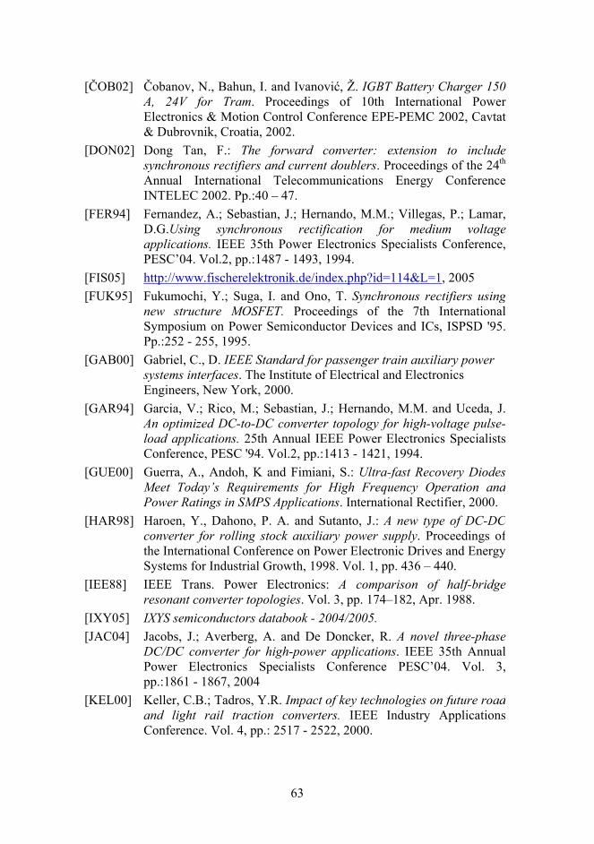
63
[ČOB02] Čobanov, N., Bahun, I. and Ivanović, Ž. IGBT Battery Charger 150 A, 24V for Tram. Proceedings of 10th International PowerElectronics & Motion Control Conference EPE-PEMC 2002, Cavtat & Dubrovnik, Croatia, 2002.
[DON02] Dong Tan, F.: The forward converter: extension to include synchronous rectifiers and current doublers. Proceedings of the 24th
Annual International Telecommunications Energy ConferenceINTELEC 2002. Pp.:40 – 47.
[FER94] Fernandez, A.; Sebastian, J.; Hernando, M.M.; Villegas, P.; Lamar, D.G.Using synchronous rectification for medium voltageapplications. IEEE 35th Power Electronics Specialists Conference,PESC’04. Vol.2, pp.:1487 - 1493, 1994.
[FIS05] http://www.fischerelektronik.de/index.php?id=114&L=1, 2005 [FUK95] Fukumochi, Y.; Suga, I. and Ono, T. Synchronous rectifiers using
new structure MOSFET. Proceedings of the 7th International Symposium on Power Semiconductor Devices and ICs, ISPSD '95.Pp.:252 - 255, 1995.
[GAB00] Gabriel, C., D. IEEE Standard for passenger train auxiliary power systems interfaces. The Institute of Electrical and Electronics Engineers, New York, 2000.
[GAR94] Garcia, V.; Rico, M.; Sebastian, J.; Hernando, M.M. and Uceda, J.An optimized DC-to-DC converter topology for high-voltage pulse-load applications. 25th Annual IEEE Power Electronics SpecialistsConference, PESC '94. Vol.2, pp.:1413 - 1421, 1994.
[GUE00] Guerra, A., Andoh, K and Fimiani, S.: Ultra-fast Recovery Diodes Meet Today’s Requirements for High Frequency Operation andPower Ratings in SMPS Applications. International Rectifier, 2000.
[HAR98] Haroen, Y., Dahono, P. A. and Sutanto, J.: A new type of DC-DC converter for rolling stock auxiliary power supply. Proceedings of the International Conference on Power Electronic Drives and EnergySystems for Industrial Growth, 1998. Vol. 1, pp. 436 – 440.
[IEE88] IEEE Trans. Power Electronics: A comparison of half-bridge resonant converter topologies. Vol. 3, pp. 174–182, Apr. 1988.
[IXY05] IXYS semiconductors databook - 2004/2005. [JAC04] Jacobs, J.; Averberg, A. and De Doncker, R. A novel three-phase
DC/DC converter for high-power applications. IEEE 35th Annual Power Electronics Specialists Conference PESC’04. Vol. 3,pp.:1861 - 1867, 2004
[KEL00] Keller, C.B.; Tadros, Y.R. Impact of key technologies on future roadand light rail traction converters. IEEE Industry Applications Conference. Vol. 4, pp.: 2517 - 2522, 2000.

64
[KHA94] Khan, I.A.: DC-to-DC converters for electric and hybrid vehicles. Power Electronics in Transportation, 1994. Proceedings, pp. 113-122.
[LAI03] Lai, Jih-Sheng. A High-Efficiency Low-Cost DC-DC Converter for SOFC. USA Future Energy Electronics Center, 2003.
[LAU02] Laugis, J., Lehtla, T., Joller, J., Boiko, V., Vinnikov, D and Lehtla, M.: Modernization of electrical transport systems in Estonia, Proceedings of 10th International Power Electronics & MotionControl Conference EPE-PEMC 2002, Cavtat & Dubrovnik, Croatia, 2002.
[LEU01] Leu, Y. H., Chen, C. L. and Chen, T. M. Analysis and design for asymmetrical half bridge forward mode converters. The proceedings of 4th IEEE International conference on Power Electronics andDrive Systems, Bali-Indonesia, Paper no.-6.4, 2001.
[MAX02] Ultracapacitor modules. Maxwell Technologies, Inc. ApplicationNote AN-003: General Sizing. 2002.
[MIN04] Min, Chen, Zhaoming, Qian and Xiaoming, Yuan: Frequency-domain analysis of uncontrolled rectifiers. Proceedings of the 19th
Annual IEEE Applied Power Electronics Conference and Exposition, APEC '04. Vol. 2, pp.:804 – 809.
[MIT00] Mitsubishi Semiconductors Power Module MOS, Databook, 2000. [MOH03] Mohan, N., Undeland, T., M., Robbins, W., P.: Power electronics:
converters, applications, and design. 3rd edition. Hoboken (N.J.): Wiley, c2003.
[NIC00] Nicolai, U., Reimann, T., Petzoldt, J. and Lutz, J.: Semikron. Application manual power modules. Verlag ISLE, 2000.
[PAS03] Pasterczyk, R.; Martin, C.; Schanen, J.L.: Semiconductors and power layout: new challenges for the optimization of high power converter. IEEE 34th Annual Power Electronics SpecialistConference, PESC '03. 2003. Vol.1, pp. 101 - 106.
[PET95] Petkov, R.: Design issues of the high-power high- frequency transformer. Proceedings of International Conference on Power Electronics and Drive Systems, 1995, (pp. 401-410, vol.1).
[POL86] Pollman, A.,J: Software Pulsewidth Modulation for MicroprocessorControl of AC Drives, IEEE Trans. Ind. Appl., Jul/Aug. 1986
[PRA88] Prasad, A.R., Ziogas, P.D.and Manias, S.: Analysis and design of a three-phase offline DC-DC converter with high frequency isolation. Conference Record of the 1988 IEEE Industry Applications Society Annual Meeting, 2-7 Oct. 1988. Pp.: 813 - 820, vol.1
[PRA91] Prasad, A.R.; Ziogas, P.D. and Manias, S. A three-phase resonant PWM DC-DC converter. 22nd Annual IEEE Power Electronics Specialists Conference, PESC '91, pp.:463 - 473, 1991.

65
[RAB90] Rabinovici, R.: Three-phase high-frequency DC-DC converter. Electronics Letters, Vol. 26, Issue 13, 21 June 1990. Pp.: 829 - 830.
[ROE01] Roehr, W., D.: Rectifier Applications Handbook: Reference Manual and Design Guide. Rev. 2, November, 2001.
[ROS98] Rossetto, L. and Spiazzi, G. Series resonant converter with wide load range. The 1998 IEEE 33-rd IAS Annual Meeting on Industry Applications Conference. Vol. 2, pp.:1326 - 1331, 1998.
[SCH02] Schuetze, T.; Berg, H. and Schilling, O. The new 6.5kV IGBT module: a reliable device for medium voltage applications, Eupec GmbH, 2002.
[SEV90] Sevems, R.: Topologies for three element resonant converters. Proceedings of the IEEE Applied Power Electronics Conference,1990, pp. 712–722.
[STE84] Steigerwald, R. L.: High frequency resonant transistor DC–DC converters. IEEE Trans. Ind. Electron., May 1984, pp. 181–191.
[STE94] Steigerwald, R. L., De Doncker, R. W. and Kheraluwala, M.H.:A comparison of high power DC-to-DC soft-switched converter topologies. Industry Applications Society Annual Meeting, 1994.Conference Record of the 1994 IEEE, 2-6 Oct. 1994, pp.1090 –1096, vol. 2.
[TOL04] Toland, M. Development of a 450 and 1200 Volt Inverter System. AIPM Program, Semikron, 2004.
[TRI97] Tricomi, N. and Adragna, C. 300w secondary controlled two-switch forward converter with l4990a. Application note by SGS Thomson, 1997.
[VOS92] Vos, P.G.E. The auxiliary power supply system for double decktrains. Proceedings of the IEE Colloquium on Auxiliary PowerSupplies for Rolling Stock, pp.1-4, 1992.
[WAL03] Walter, J. and De Doncker, R.W. High-power galvanically isolated DC/DC converter topology for future automobiles. 34th IEEE Power Electronics Specialist Conference, PESC '03. Vol.1, pp.:27 - 32, 2003
[ZIO90] Ziogas, P.D et al.: A refined PWM scheme for Voltage and CurrentSource Inverters, in Conf. Rec. of the 1990. IEEE IAS Annual Meeting, pp. 977-983.
[ZVE00] Zverev, I. and Hancock, J.: CoolMOS Selection Guide. Infineon Technologies AG Application Note. AN-CoolMOS-02, 2000.
[ZWI98] Zwietnig, G.: Have we reached the end of the road? DATEL GmbH December, 1998.
66
Abstract This doctoral work has developed a theoretical and practical knowledge base related to DC/DC voltage converters for the rolling stock applications. A new power scheme topology for improving power density and reducing component stresses and system volume for the implementation in the onboard APS converters has been recommended, analyzed and tested. The designed and implemented auxiliary power supply for the light rail vehicle (TSM1) is the most important practical value. It provides a real advancement in converters’ techniques for the rolling stock. The energy consumption of the onboard low-voltage power supply system as well as maintenance costs of the APS converter can be significantly reduced using the new proposed converter. In contrast to the recently popular full-bridge single-phase topology, the proposed new full-bridge isolated DC/DC converter topology with a three-phase intermediate AC-link allows for a reduction of over 30% of an average inverter switch and rectifier diode current (i.e., minimization of steady-state losses of IGBTs and free-wheeling diodes and conduction losses of secondary rectifiers). Due to a dramatic increase in the output ripple frequency (three times the output ripple frequency of the compared FBSP topology) the values of output LC-filter components are more than 60% lower (compared to the FBSP topology) for the same transferred power. As the size minimization of the magnetic components is a basic trend in modern power electronics, this advantage of the proposed topology is substantial. The new developed and implemented auxiliary power supply converter TSM1 (based on the new proposed topology) allows a 35% reduction of energy consumption by the LRV onboard low-voltage power supply (verified on the tram ČKD KT4), occupies less space and is very lightweight (volume reduced up to 30% and weight reduced up to 40% in comparison with recent European analogues), very powerful (a 50% improvement of the output current capability), has very flexible control, which allows using it with the minimal changes in different LRV types and on the trolleybuses as well as in some industrial applications. The author was granted one Estonian Utility Model Certificate (EE00331U1) for the design of the proposed system (APS converter TSM1).

67
Kokkuvõte Käesolev doktoritöö analüüsib suurevõimsuseliste isoleeritud alalispingemuundurite arendusprobleeme. Muundurid on mõeldud kasutamiseks kergrööbassõidukite madalpingelistes toitesüsteemides. Töö käsitleb veeremi jõupooljuhtmuunduritega seotud tehnilisi raskusi ning annab ülevaate tehnoloogia nüüdistasemest selles valdkonnas. Töö sisaldab klassifikatsioonide, projekteerimisnõuete, topoloogiate, komponentide ja optimeerimismeetodite analüüsi. Välja on pakutud sildlülitusega alalispingemuunduri topoloogia, milles kasutatakse kolmefaasilist vahelduvvoolulüli. Kirjeldatud lahendus on suurepärane alternatiiv praegu kergrööbassõidukite madalpingelistes toitesüsteemides kasutusel olevatele ühefaasilistele sildlülitustega alalispingemuundurite topoloogiatele. Tänu uuele topoloogiale paraneb oluliselt suurevõimsuselise muunduri võimsustihedus ja väheneb komponentide koormus. Tänu väiksemate mõõtmetega filtritele avaneb võimalus muuta konstruktsioon kompaktsemaks. Hüpoteesid on kontrollitud võrdleva analüüsi, virtuaalse modelleerimise ja katsetustega. Töö praktiline osa käsitleb kõrgsageduslike vaheldi- ja alaldiastmete projekteerimist ning kompaktse konstruktsiooni loomise võimalusi koos uute jahutustehnoloogiate kasutamisega. Väljatöötatud uus kolmefaasilise kõrgsagedusliku vaheldi juhtimismeetod (pingevektori pulsilaiusmodulatsiooni lihtsustatud variant) võimaldab vaheldi pooljuhtlülitite paindlikku juhtimist alalisvoolulüli pinge parendatud kasutuse tõttu. Doktoritöö suurim praktiline väärtus on kaheväljundilise abitoitemuunduri TSM1 väljatöötamine ja rakendamine trammil ČKD KT4. Loodud muundur on teiste uuemate Euroopa analoogidega võrreldes väga kompaktne (15..30% väiksemate mõõtmetega ja kuni 40% väiksema kaaluga). Muundur on võimas (50% suurema väljundvoolu maksimaalväärtusega) ning väga paindliku juhtimisega, mis väheste muudatustega võimaldab selle kasutamist edaspidi ka teistel kergrööbassõidukitel ning elektertranspordivahenditel (rongid, trollibussid, jne.) aga ka tööstuslikes rakendustes. Lahendus on kasutusel Tallinna trammides ning on kaitstud Eesti kasuliku mudeli tunnistusega.

68
Author’s main publications 1. Laugis, J., Vinnikov, D. and Boiko, V.: "Analysis of drawbacks and reconstruction
problems of the R2-type train". Proceedings of the 7th Baltic Electronics Conference BEC’2000. ISBN 9985-59-179-8, pp. 355-358. Tallinn, 2000.
2. Ю. Лаугис, Т. Лехтла, Ю. Йоллер, В. Бойко, Д. Винников, М. Лехтла “Состояние и тенденции развития электротранспорта Эстонии” (in Russian). Proceedings of the 3rd International conference of Variable Speed Drives. ISBN 5-93126-018-8, pp. 243-245. Nizhny Novgorod, 2001.
3. Lehtla, M. and Vinnikov, D.: "Supply for the Auxiliary Systems in the Rail Vehicle". Proceedings of the 3th Research Symposium of Young Scientists “Actual Problems of Electrical Drives and Industry Automation". ISBN 9985-69-020-6, pp. 68-70. Tallinn, 2001.
4. B. Бойко, Д. Винников, Ю. Лаугис, С. Игнатов. “Модернизация установки “Universalprüfmaschine Zwick 1435” на Пярнуской лыжной фабрике” (in Russian). Proceedings of the International Conference „Automation and Control Technologies - 2002”. ISBN 9955-09-183-5, pp. 9-11. Kaunas, Lithuania, 2002.
5. Д. Винников, В. Бойко, Ю. Лаугис “Разработка и исследование статического преобразователя напряжения для трамвая” (in Russian). Proceedings of the International Conference “Силовая электроника и энергоэффективность СЭЭ’2002”, ISSN 0204-3599, vol. 1., pp. 3-6. Alushta, Ukraine, 2002.
6. D. Vinnikov, M.Lehtla, J.Joller, J. Laugis. ”Research and development of voltage converter for trams”. Proceedings of the International Conference “Power and Electrical Engineering”, ISSN 1407-7345, pp. 72-76. Riga, Latvia, 2002.
7. Laugis, J., Lehtla, T., Joller, J., Boiko, V., Vinnikov, D., Lehtla, M. “Modernization of Electrical Transport Systems in Estonia”. Proceedings of the 10th International Power Electronics and Motion Control Conference EPE-PEMC’2002. ISBN 953-184-046-6, p. 449. Cavtat & Dubrovnik, Croatia, 2002.
8. V. Boiko, D. Vinnikov, J. Joller: “Use of ultracapacitor modules in ICE starting system”. Proceedings of the International Conference “Power and Electrical Engineering”, ISSN 1407-7345, pp. 66-71. Riga, Latvia, 2002.
9. Boiko, V., Vinnikov, D. and Joller J.: “Starting of a Diesel Engine by Help of Ultracapacitors” Proceedings of the 8th Baltic Electronics Conference BEC’2002. ISBN 9985-59-292-1, pp. 405-406. Tallinn, 2002.
10. Vinnikov, D.: “Solving EMI Problems of a High-Frequency DC-DC Converter”. Proceedings of the 4th Research Symposium of Young Scientists “Actual Problems of Electrical Drives and Industry Automation”, ISBN 9985-69-027-3, pp. 69-72. Tallinn, 2003.
11. Vinnikov, D., Lehtla, T. and Joller, J.: “EMI Problems of the High-Frequency Three-Phase Rectifier”. Proceedings of the 3rd International Workshop on Compatibility in Power Electronics CPE’2003, ISBN 83-88317-03-2, pp. 159-161. Gdansk-Zielona Góra, Poland, 2003.
12. Винников, Д., Бойко, В., Лаугис, Ю.: “Исследование возможностей применения ультраконденсаторов в электросистеме автомобиля” (in Russian). Proceedings of the International Conference “Силовая электроника и энергоэффективность СЭЭ’2003”, ISSN 0204-3599, vol.3., pp. 27-30. Alushta, Ukraine, 2003.

69
13. Vinnikov, D., Lehtla, T.: „Review of Possible DC-DC Converter Topologies for Tram’s Auxiliary Power Supply“. Proceedings of the 10th International Power Electronics and Motion Control Conference EPE-PEMC’2004, ISBN 9984-32-070-7, vol. 6, pp. 176-179. Riga, Latvia, 2004.
14. Vinnikov, D.: “Auxiliary Voltage Converter for Tallinn Trams: Stages of Development“. Proceedings of the International Symposium “Topical Problems of Education in the Field of Electrical and Power Engineering“, ISBN 9985-69-030-3, pp. 62-65. Kuressaare, 2004.
15. Бойко, В., Винников, Д., Лаугис, Ю.: “Решение задачи измерения скорости в макете привода с векторным управлением“ (in Russian). Proceedings of the International Conference „Automation and Control Technologies - 2004”. ISBN 9955-09-644-6, pp. 43-45. Kaunas, Lithuania, 2004.
16. Винников, Д., Бойко, В., Лехтла, М., Росин, А., Лаугис, Ю.: „Об опыте института электропривода и силовой электроники ТТУ в области модернизации электроподвижного состава Таллиннского трамвайного парка“ (in Russian). Proceedings of the International Conference “Силовая электроника и энергоэффективность СЭЭ’2004”, ISSN 0204-3599, vol.3., pp. 52-55. Alushta, Ukraine, 2004.
17. Vinnikov, D. and Lehtla, T.: „Compact Design of a Power circuit for a Dual-Output Voltage Converter”, Proceedings of the 9th Baltic Electronics Conference BEC’2004. ISBN 9985-59-462-2, pp. 333-336. Tallinn, 2004.
18. Laugis, J., Lehtla, T., Pettai, E., Joller, J., Rosin, A., Lehtla, M., Vinnikov, D.: “Modernisation of Trams in Estonia”, Proceedings of the International Conference “Unconventional Electromechanical and Electrical systems UEES’2004“, ISBN 83-88764-19-5, vol. 2, pp. 561-564. Alushta, Ukraine, 2004.
19. Vinnikov, D. and Lehtla, T. “Influence of Specific Requirements on the Design of Auxiliary Power Supply for a Light Rail Vehicle“. Proceedings of the 2nd International Symposium “Topical Problems of Education in the Field of Electrical and Power Engineering“, ISBN 9985-69-033-8, pp. 93-97. Kuressaare, 2005.
20. Бойко, В., Винников, Д.: “Об опыте проведения курсов повышения квалификации в Институте электропривода и силовой электроники Таллиннского Технического Университета“ (in Russian). Proceedings of the International Conference „Automation and Control Technologies - 2005”. ISBN 9955-09-864-3, pp. 15-17. Kaunas, Lithuania, 2005.
21. Vinnikov, D., Lehtla, T.: “Overvoltages in the Inverter-Fed AC Motor Systems with Long Cables”. Proceedings of the 4th International Workshop on Compatibility in Power Electronics CPE’2005, ISBN 83-7421-075-3, pp. 69-71. Gdynia, Poland, 2005.
Intellectual Property 1. Registered Utility Model Certificate “High frequency auxiliary power supply for
Electric Vehicles”; Estonian Patent Office, reg. nr. EE00331U1. Applicant: Tallinn University of Technology. Authors: D. Vinnikov, J. Joller, M. Lehtla, O. Kiritsenko, J. Laugis. Date of issue: 15.10.2002.

70
LISA / ANNEX 1
ELULOOKIRJELDUS 1. Isikuandmed
Ees- ja perekonnanimi: Dmitri Vinnikov Sünniaeg ja -koht: 07.04.1976, Tallinn Kodakondsus: Eesti Perekonnaseis: abielus Lapsed: - 2. Kontaktandmed Aadress: Vikerlase 13-21, 13616, Tallinn Telefon: (+372) 51907446 E-posti aadress: [email protected] 3. Hariduskäik Õppeasutus (nimetus lõpetamise ajal)
Lõpetamise aeg
Haridus (eriala/kraad)
Tallinna Tehnikaülikool 2001 tehnikateaduste magister, elektriajamid ja jõuelektroonika
Tallinna Tehnikaülikool 1999 diplomeeritud insener, robotitehnika Tallinna 25. Keskkool 1993 põhiharidus 4. Keelteoskus (alg-, kesk- või kõrgtase) Keel Tase Vene Kõrgtase Inglise Kesktase Vene Kesktase 5. Teenistuskäik
Töötamise aeg Ülikooli, teadusasutuse või muu organisatsiooni nimetus
Ametikoht
06. - 08.1998 AS Estel Pluss spetsialist 07. - 08.1999 Tallinna Tehnikaülikool insener 08.1999 - Tallinna Tehnikaülikool teadur 09. - 11.2000 Brandenburgi Tehnikaülikool Cottbusis teadur 6. Täiendõpe Õppimise aeg Õppeasutuse või muu organisatsiooni nimetus 2003 TTÜ sisekoolituskursus teemal “Projektijuhtimine” 2003 TTÜ sisekoolituskursus teemal “Intellektuaalomandi ja
patendinduse alused”

71
7. Teadustegevus 2005 510L “AS BLRT ERA 10t kandejõuga sildkraana juhtimise
moderniseerimine” (siseriiklik leping) 2003-2007 T513 “Energiamuundus- ja -vahetusprotsesside uurimine
elektriajamite ja pooljuhtmuundurite jõuvõrkudes” (HM sihtfinantseerimine)
2004 T002 “Elektritranspordi ajami- ja automaatikasüsteemid” (HM sihtfinantseerimine)
2002-2004 245F “Elektritranspordi veoajamid, automaatika- ja infosüsteemid” (ESTAG arendustoetus)
2001-2003 G4852 “Elektriajamite ja jõupooljuhtmuundurite parameetrite diagnostika talitluse tõhustamiseks ja töökindluse suurendamiseks” (ETF uurimistoetus)
2002 202L “Trammide elektriajamite ja jõumuundurite moderniseerimine” (siseriiklik leping)
2001 130L “Elektriraudtee kontaktvõrgu ja veoalajaamade tehnilise seisundi uuring” (siseriiklik leping)
2001 126L “Trammi staatilise pingemuunduri väljatöötamine” (siseriiklik leping)
2000 4/011L “Elektriveduri ER2 peaveoajami tehnilis-majanduslike näitajate analüüs ja ettepanekud moderniseerimiseks” (siseriiklik leping)
2001-2002 105L “Trammide veoajamite rekonstrueerimine” (siseriiklik leping)
1999-2001 920F “Trammide elektri-, signalisatsiooni-, andmeside- ja infosüsteemide pilootprojekt” (ESTAG arendustoetus)
8. Kaitstud lõputööd • “Elektriauto energiavarustus” (diplomitöö, 1999) • “Trammi abitoiteallikas” (magistritöö, 2001)
9. Teadustöö põhisuunad
• Rööbassõidukite abitoitemuundurite ja veomuundurite probleemide analüüs ning uute meetodite ja süsteemide välmimine
10. Teised uurimisprojektid
• Ülikondensaatorite kasutamine sõidukites, sammuvate ekskavaatorite energeetilised mõõtmised, kraanade moderniseerimine
Kuupäev: 25.07.06.

72
CURRICULUM VITAE 1. Personal information Name: Dmitri Vinnikov
Date and place of birth: 07.04.1976, Tallinn Citizenship: Estonian Marital status: married Children: no
2. Contact information
Address: Vikerlase 13-21, 13616, Tallinn Telephone: (+372) 51907446 E-mail: [email protected]
3. Educational history Institution
Graduation date
Education
Tallinn University of Technology
2001 M.Sc., Electrical Drives and Power Electronics
Tallinn University of Technology
1999 Dipl. Eng, Robotics
Tallinn Secondary School No 25
1993 Basic
4. Languages
Language Level Russian Excellent English Good Estonian Good 5. Professional employment
Date Organization Position 06. - 08.1998 Estel Pluss Ltd. Specialist 07. - 08.1999 Tallinn University of Technology Engineer 08.1999 - Tallinn University of Technology Researcher 09. - 11.2000 Brandenburg Technical university Cottbus Researcher 6. Special courses
Date Organization 2003 “Project Management”, Tallinn University of Technology 2003 “Basics of Patents and Intellectual Property”, Tallinn
University of Technology
73
7. Scientific work
2005 510L “Modernization of the 10t Bridge Crane”, contract
2003-2007 T513 “Energy conversion and exchange processes in power networks of electrical drives and semiconductor converters”, target finance-based main topic
2004 T002 “Drive and automation for electricity-driven vehicles”, Funded by the Ministry of Education and Research
2002-2004 245F “Traction drives, automation and information systems”, Enterprise Estonia support contract
2001-2003 G4852 “Diagnostics of electrical drives and power semiconductor converters for improvement of operation and reliability”, Estonian Science Foundation grant
2002 202L “Modernization of electrical drives and power converters of trams”, contract
2001 130L ”Investigation of catenary system on the Estonian Railway”, contract
2001
126L “Development of auxiliary power supply for the tram KT4”, contract
2000 4/011L “Analysis of drawbacks and reconstruction problems of the commuter train ER2”, contract
2001-2002 105L “Reconstruction of tram traction drives”, contract
1999-2001 920F “Trams electrical, signalization, communication, information systems pilot project”, Enterprise Estonia support contract
8. Theses • Energy Supply of Electric Vehicle, (1999, Dipl. Eng) • Auxiliary power supply for a tram, (2001, M.Sc.)
9. Main areas of scientific work
• Auxiliary power supplies and traction drives of Electrical Rail Vehicles - analysis of common problems and development of new methods, solutions and systems
10. Other Research Projects
• Investigation of ultracapacitors in automotive applications, electric measurements on Draglines and commuter trains, renovation of cranes, etc.
Date: 25.07.06.