Embed Size (px)
Citation preview
Research ArticleMATLAB User Interface for Simulation of Silicon GermaniumSolar Cell
Ashish Kumar Singh, Jahnvi Tiwari, Ashish Yadav, and Rakesh Kumar Jha
School of Electronics and Communication, Shri Mata Vaishno Devi University, Katra 182320, India
Correspondence should be addressed to Ashish Kumar Singh; [email protected]
Received 22 June 2015; Revised 24 July 2015; Accepted 5 August 2015
Academic Editor: Rodrigo Martins
Copyright © 2015 Ashish Kumar Singh et al. This is an open access article distributed under the Creative Commons AttributionLicense, which permits unrestricted use, distribution, and reproduction in any medium, provided the original work is properlycited.
Nuclear fusion reaction on the sun is the largest source of energy. In this paper, qualitative investigation of the numerical model ofsilicon germanium heterojunction solar cell is performed using MATLAB graphical user interface.The heterostructure is designedas Si1−𝑥Ge𝑥 for speculative determination of appropriate germanium mole fraction to get the maximized thin-film solar cellefficiency ( ́𝜂). Other characteristics such as absorption coefficient (𝛼), energy band gap (𝐸
𝑔SiGe), reflectivity (r), open circuit voltage
(𝑉oc), and generation rate (𝐺(𝜆, 𝑥)) are also considered.This user interfacewill reduce the complexity of solving differential equationfor the analysis of silicon germanium heterojunction cell.
1. Introduction
Due to the constant increase in pressure on the nonrenewableenergy sources, renewable energy sources are gaining popu-larity. Solar cell is an efficient type of renewable energy source.As compared to Si, Ge has steeper absorption edge andgenerally optical absorption coefficient of Ge is higher thanthat of Si. Silicon junction is stacked on top of a germaniumjunction for the enhancement of efficiency from a singlejunction Si solar cell [1].The SiGe absorption behavior resultsin current gain, but at same time energy band gap of SiGedecreases. Various analyses on thin-film SiGe solar cells arecarried to improve the characteristics and efficiency [2].
Heterojunction solar cells have a great advantage ofachieving high electrical voltage [3] because material withlarge band has low minority charge concentration whichleads to minimum recombination at the interface. For selec-tion of better solar cell, semiconductor should be chosen onthe basis of spectrum absorption [4]. Semiconductors likesilicon and germanium have indirect band gap as shownin Figure 1 and it is used as an absorber in solar cell [5].If we introduce Ge content in SiGe alloy its indirect bandgap decreases. The main function of any indirect band gapsemiconductor is trapping light; this can be enhanced byoptimum texturing. Indirect band gap semiconductor also
has high recombination lifetime and large diffusion length[6, 7].
Section 2 features the user interface. Section 3 includesthe work of software interface; the structure of SiGe solar cellis modelled in Section 4. Section 5 focuses on the propertiesof SiGe alloy. Simulation results are presented in Section 6with the simulated data.
2. User Interface Features
The purpose of this user interface is to develop a generalpurpose solar device simulator that is functional andmodularin nature to allowflexibility during programming andprovidesufficient scope for future developments. In addition, theprogram’s main goal is to provide a tool that can supplementsolar cell modeling, device physics and to construct basiccell equations using MATLAB tools. MATLAB’s capabilityand inherent nature of handling matrices and matrix oper-ations make it an optimum software for numerical analysisalgorithms. A device modeling program is developed usingbasic MATLAB tools necessary to understand the operationof the program. The program solution will be used toexamine device parameters such as carrier statistics, devicepotential, and internal electric fields. The device solution iscompared to the analytical approximations in order to further
Hindawi Publishing CorporationJournal of MaterialsVolume 2015, Article ID 840718, 6 pageshttp://dx.doi.org/10.1155/2015/840718
2 Journal of Materials
Direct band gap Indirect band gap
Photon emissionPhoton emission
Phonon emissionMomentum
Indirect band gapenergy
Direct band gapenergy
Conduction band (Ec)
Valance band (E�)
Figure 1: Direct and indirect band gap.
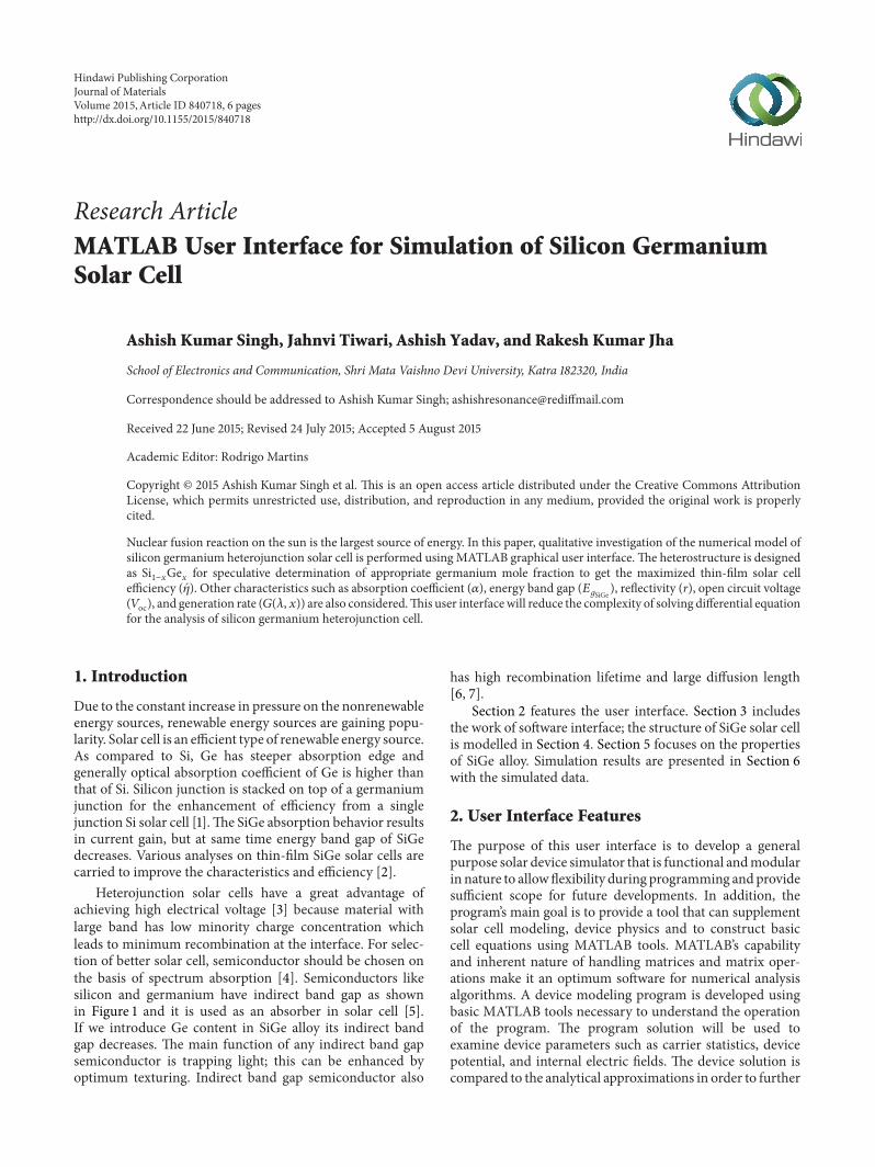
Figure 2: MATLAB GUI.
strengthen the understanding between theory and exactnumerical solutions and how those solutions are obtained.In this software, silicon germanium solar cell analysis canbe performed easily. Cell structure dimension is used withpredefined parameters and electrical properties to solve thecomplex equation internally to provide best and instantresult. Properties of silicon and germanium are prestored inGUI.
3. Graphical User Interface Working
Figure 2 shows the main window of this program. Initially,incident optical power is selected and different parameterslike temperature, texturing factor, front reflectivity, devicearea, and device parameters are defined. In this program,properties of silicon and germanium are predefined, it canalso be changed (increase digit after decimal), as per require-ment for exact result, with the help of “Settings” button. Resetbutton is used to reconfigure the whole window except thepredefined parameters. Button labeled as “Structure Define”is used for designing the layout of heterojunction Si/SiGesolar plate layer. Structure design is linked to new graphicaluser interface where it is loaded for further configurationsettings of the model. Here, parameters like concentration,thickness of Si, SiGe, and lifetime of minority carrier (𝜏p),along with mole fraction range, are required.
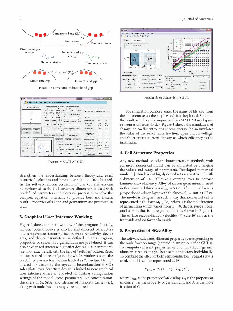
Figure 3: Structure define GUI.
For simulation purpose, enter the name of file and fromthe popmenu select the graphwhich is to be plotted. Simulatethe result, which can be imported fromMATLAB workspaceor from a different folder. Figure 3 shows the simulation ofabsorption coefficient versus photon energy. It also simulatesthe value of the exact mole fraction, open circuit voltage,and short circuit current density at which efficiency is themaximum.
4. Cell Structure Properties
Any new method or other characterization methods withadvanced numerical model can be simulated by changingthe values and range of parameters. Developed numericalmodel [9]: thin layer of highly doped n-Si is constructed witha dimension of 5 × 10
−9m as a capping layer to increaseluminescence efficiency. Alloy of silicon germanium is usedin this layer and thickness 𝑑SiGe is 50 × 10
−9m. Final layer isp-type doped silicon layer with thickness 𝑑Si = 100 × 10
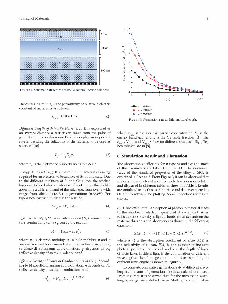
−9m.The model is designed in such a way that numerical cell isrepresented in the formSi1−𝑥Ge𝑥, where𝑥 is themole fractionof germanium which varies from 𝑥 = 0, that is, pure silicon,until 𝑥 = 1, that is, pure germanium, as shown in Figure 4.The surface recombination velocities (𝑆
𝑃
) are 102m/s at thefront side and∞ for the backside.
5. Properties of SiGe Alloy
The software calculates different properties corresponding tothe mole fraction range (entered in structure define GUI 1).To compute different properties of alloy of silicon germa-nium, we need to analyze both semiconductors individually.To combine the effect of both semiconductors, Vegard’s law isused, and this can be represented as [9]
𝑃SiGe = 𝑃Si (1−𝑋) +𝑃Ge (𝑋) , (1)
where 𝑃SiGe is the property of SiGe alloy, 𝑃Si is the property ofsilicon, 𝑃Ge is the property of germanium, and 𝑋 is the molefraction of Ge.
Journal of Materials 3
5nm
50nm
100nm
n+ Si
n− SiGe
p− Si
p+ Si
Figure 4: Schematic structure of Si/SiGe heterojunction solar cell.
Dielectric Constant (𝜀𝑟
).The permittivity or relative dielectricconstant of material is as follows:
𝜀
𝑟SiGe=11.9+ 4.1𝑋. (2)
Diffusion Length of Minority Holes (𝐿
𝑝
). It is expressed asan average distance a carrier can move from the point ofgeneration to recombination. Parameters play an importantrole in deciding the suitability of the material to be used assolar cell [10]
𝐿
𝑝
= √𝐷
𝑝
𝜏
𝑝
, (3)
where 𝜏𝑝
is the lifetime of minority holes in n-SiGe.
Energy Band Gap (𝐸
𝑔
). It is the minimum amount of energyrequired for an electron to break free of its bound state. Dueto the different thickness of Si and Ge alloys, the stackedlayers are formedwhich relates to different energy thresholds,absorbing a different band of the solar spectrum over a widerange from silicon (1.12 eV) to germanium (0.66 eV). Fortype-I heterostructure, we use the relation
Δ𝐸
𝑔
= Δ𝐸V +Δ𝐸
𝑐
. (4)
Effective Density of States in Valence Band (𝑁V). Semiconduc-tor’s conductivity can be given by the relation
(𝜎) = 𝑞 (𝜇
𝑛
𝑛 + 𝜇
𝑝
𝑝) , (5)
where 𝜇
𝑛
is electron mobility, 𝜇𝑝
is hole mobility, 𝑛 and 𝑝
are electron and hole concentration, respectively. Accordingto Maxwell-Boltzmann approximation, 𝑝 depends on 𝑁V(effective density of states in valence band).
Effective Density of States in Conduction Band (𝑁
𝑐
). Accord-ing to Maxwell-Boltzmann approximation, 𝑛 depends on 𝑁
𝑐
(effective density of states in conduction band)
𝑛
2𝑖SiGe
= 𝑁
𝑐SiGe𝑁VSiGe𝑒
[−𝐸𝑔/𝐾𝑇]
, (6)
0 1 2 3 4 5
×1029
x (m)
𝜆 = 490nm𝜆 = 710nm𝜆 = 990nm
0
1
2
3
4
Gen
erat
ion
rate
(G) (
(m3s)
−1) 5
6
×10−8
Figure 5: Generation rate at different wavelength.
where 𝑛
𝑖SiGeis the intrinsic carrier concentration, 𝐸
𝑔
is theenergy band gap, and 𝑥 is the Ge mole fraction [11]. The𝑛
𝑖SiGe,𝑁VSiGe , and𝑁
𝑐SiGevalues for different 𝑥 values in Si1−𝑥Ge𝑥
heterolayers are in [9].
6. Simulation Result and Discussion
The absorption coefficients for 𝑛 type Si and Ge and mostof the parameters are taken from [12, 13]. The numericalvalue of the simulated properties of the alloy of SiGe isexplained in Section 3. From Figure 2, it can be observed thatimportant parameter at specified mole fraction is calculatedand displayed in different tables as shown in Table 1. Resultsare simulated using this user interface and data is exported toOriginPro software for plotting. Some important results areshown.
6.1. Generation Rate. Absorption of photon in material leadsto the number of electrons generated at each point. Afterreflection, the intensity of light to be absorbed depends on thematerial thickness and absorption as shown in the followingequation:
𝐺 (𝜆, 𝑥) = 𝛼 (𝜆) 𝐹 (𝜆) [1−𝑅 (𝜆)] 𝑒
−𝛼(𝜆)𝑥
, (7)
where 𝛼(𝜆) is the absorption coefficient of SiGe, 𝑅(𝜆) isthe reflectivity of silicon, 𝐹(𝜆) is the number of incidentphotons per area per second, and 𝑥 is the depth of layerof SiGe layer. Incident light is the combination of differentwavelengths; therefore, generation rate corresponding todifferent wavelengths is shown in Figure 5.
To compute cumulative generation rate at different wave-lengths, the sum of generation rate is calculated and used.From Figure 5, it is observed that, for the increase in wave-length, we get new shifted curve. Shifting is a cumulative
4 Journal of Materials
Table 1: Value of different properties as a function of mole fraction of germanium (𝑥).
Properties of Si1−𝑥Ge𝑥 Si Si0.9Ge0.1 Si0.85Ge0.15 Si0.8Ge0.2 Si0.75Ge0.25 Si0.7Ge0.3 Ge𝜀
𝑟
11.9 12.31 12.51 12.72 12.92 13.13 16𝐸
𝑔
(ev) 1.12 1.074 1.051 1.028 1.005 0.982 0.66𝐷
𝑝
(m2/s) 2.458 × 10⁻⁴ 2.419 × 10⁻⁴ 2.399 × 10⁻⁴ 2.38 × 10⁻⁴ 2.361 × 10⁻⁴ 2.341 × 10⁻⁴ 2.07 × 10⁻⁴
𝐷
𝑛
(m2/s) 6.986 × 10⁻⁴ 7.193 × 10⁻⁴ 7.3 × 10⁻⁴ 7.40 × 10⁻⁴ 7.50 × 10⁻⁴ 7.60 × 10⁻⁴ 9.056 × 10⁻⁴
𝐿
𝑝
(m) 1.567 × 10⁻⁵ 1.554 × 10⁻⁵ 1.549 × 10⁻⁵ 1.542 × 10⁻⁵ 1.536 × 10⁻⁴ 1.529 × 10⁻⁵ 1.438 × 10⁻⁵
𝑁V (cm−3) 1.04 × 10¹⁹ 9.96 × 10¹⁸ 9.74 × 10¹⁸ 9.52 × 10¹⁸ 9.3 × 10¹⁸ 9.08 × 10¹⁸ 6 × 10¹⁸
𝑁
𝑐
(cm−3) 2.8 × 10¹⁹ 2.62 × 10¹⁹ 2.53 × 10¹⁹ 2.44 × 10¹⁹ 2.36 × 10¹⁹ 2.27 × 10¹⁹ 1.04 × 10¹⁹
𝑛
𝑖
(cm−3) 1.45 × 10¹⁰ 2.413 × 10¹² 3.612 × 10¹² 4.81 × 10¹² 6.01 × 10¹² 7.21 × 10¹² 2.4 × 10¹³
400 600 800 1000 1200 1400200Wavelength (nm)
𝛼
r
10−8
10−6
10−4
10−2
100
102
104
106
Abso
rptio
n co
effici
ent (𝛼)
(cm
−1)
0.3
0.4
0.5
0.6
0.7
0.8
Refle
ctiv
ity (r
)
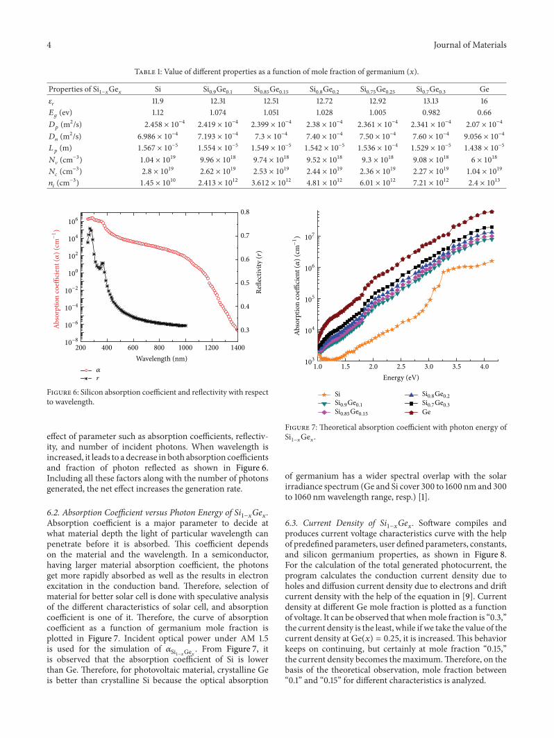
Figure 6: Silicon absorption coefficient and reflectivity with respectto wavelength.
effect of parameter such as absorption coefficients, reflectiv-ity, and number of incident photons. When wavelength isincreased, it leads to a decrease in both absorption coefficientsand fraction of photon reflected as shown in Figure 6.Including all these factors along with the number of photonsgenerated, the net effect increases the generation rate.
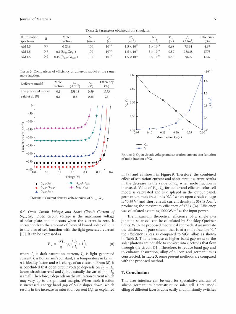
6.2. Absorption Coefficient versus Photon Energy of Si1−𝑥
Ge𝑥
.Absorption coefficient is a major parameter to decide atwhat material depth the light of particular wavelength canpenetrate before it is absorbed. This coefficient dependson the material and the wavelength. In a semiconductor,having larger material absorption coefficient, the photonsget more rapidly absorbed as well as the results in electronexcitation in the conduction band. Therefore, selection ofmaterial for better solar cell is done with speculative analysisof the different characteristics of solar cell, and absorptioncoefficient is one of it. Therefore, the curve of absorptioncoefficient as a function of germanium mole fraction isplotted in Figure 7. Incident optical power under AM 1.5is used for the simulation of 𝛼Si1−𝑥Ge𝑥 . From Figure 7, itis observed that the absorption coefficient of Si is lowerthan Ge. Therefore, for photovoltaic material, crystalline Geis better than crystalline Si because the optical absorption
1.5 2.0 2.5 3.0 3.5 4.01.0Energy (eV)
103
104
105
106
107
Abso
rptio
n co
effici
ent (𝛼)
(cm
−1)
SiSi0.9Ge0.1Si0.85Ge0.15
Si0.8Ge0.2Si0.7Ge0.3Ge
Figure 7: Theoretical absorption coefficient with photon energy ofSi1−𝑥
Ge𝑥
.
of germanium has a wider spectral overlap with the solarirradiance spectrum (Ge and Si cover 300 to 1600 nm and 300to 1060 nm wavelength range, resp.) [1].
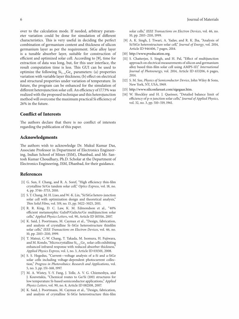
6.3. Current Density of Si1−𝑥
Ge𝑥
. Software compiles andproduces current voltage characteristics curve with the helpof predefined parameters, user defined parameters, constants,and silicon germanium properties, as shown in Figure 8.For the calculation of the total generated photocurrent, theprogram calculates the conduction current density due toholes and diffusion current density due to electrons and driftcurrent density with the help of the equation in [9]. Currentdensity at different Ge mole fraction is plotted as a functionof voltage. It can be observed that whenmole fraction is “0.3,”the current density is the least, while if we take the value of thecurrent density at Ge(𝑥) = 0.25, it is increased.This behaviorkeeps on continuing, but certainly at mole fraction “0.15,”the current density becomes themaximum.Therefore, on thebasis of the theoretical observation, mole fraction between“0.1” and “0.15” for different characteristics is analyzed.
Journal of Materials 5
Table 2: Parameters obtained from simulator.
Illuminationspectrum 𝑅
Molefraction
𝑆
𝑃
(m/s)𝜏
𝑝
(s)𝑁
𝐴
(m−3)𝑁
𝐷
(m−3)𝑉oc(V)
𝐽sc(A/m2)
Efficiency(%)
AM 1.5 0.9 0 (Si) 100 10−8 1.5 × 10²² 5 × 1025 0.68 78.94 4.67AM 1.5 0.9 0.1 (Si0.9Ge0.1) 100 10−8 1.5 × 10²² 5 × 1025 0.59 358.18 17.73AM 1.5 0.9 0.15 (Si0.85Ge0.15) 100 10−8 1.5 × 10²² 5 × 1025 0.56 382.5 17.47
Table 3: Comparison of efficiency of different model at the samemole fraction.
Different model Molefraction
𝐽sc(A/m2)
𝑉oc(V)
Efficiency(%)
The proposed model 0.1 358.18 0.59 17.73Said et al. [8] 0.1 183 0.55 7.5
−400
−350
−300
−250
−200
−150
−100
−50
0
0.1 0.2 0.3 0.4 0.5 0.60.0Voltage (V)
Si0.9Ge0.1Si0.85Ge0.15
Si0.75Ge0.25
Si0.8Ge0.2Si0.7Ge0.3
Curr
ent d
ensit
y (A
/m2)
Figure 8: Current density voltage curve of Si1−𝑥
Ge𝑥
.
6.4. Open Circuit Voltage and Short Circuit Current ofSi1−𝑥
Ge𝑥
. Open circuit voltage is the maximum voltageof solar plate and it occurs when the current is zero. Itcorresponds to the amount of forward biased solar cell dueto the bias of cell junction with the light generated current[10]. It can be expressed as
𝑉oc =𝑛𝑘𝑇
𝑞
log𝑒
(
𝐼
𝐿
𝐼
𝑠
+ 1) , (8)
where 𝐼
𝑠
is dark saturation current, 𝐼𝐿
is light generatedcurrent, 𝑘 is Boltzmann’s constant,𝑇 is temperature in kelvin,𝑛 is ideality factor, and 𝑞 is charge of an electron. From (8), itis concluded that open circuit voltage depends on 𝐼
𝐿
= 𝐼sc(short circuit current) and 𝐼
𝑠
, but actually the variation of 𝐼scis small.Therefore, it depends on the saturation currentwhichmay vary up to a significant margin. When mole fractionis increased, energy band gap of SiGe slopes down, whichresults in the increase in saturation current (𝐼
𝑠
), as explained
0.45
0.50
0.55
0.60
0.65
Is
×10−7
0.10 0.15 0.20 0.25 0.300.050.0
0.4
0.8
1.2
1.6
I s(A
/m2)
Mole fraction Ge(x)
Voc
(V)
Voc
Figure 9: Open circuit voltage and saturation current as a functionof mole fraction of Ge.
in [9] and as shown in Figure 9. Therefore, the combinedeffect of saturation current and short circuit current resultsin the decrease in the value of 𝑉oc when mole fraction isincreased. Value of 𝑉oc, 𝐽sc for better and efficient solar cellmodel is calculated and is displayed in the output panel:germaniummole fraction is “0.1,” where open circuit voltageis “0.59V” and short circuit current density is 358.18 A/m2,producing the maximum efficiency of 17.73 (%). Efficiencywas calculated assuming 1000W/m2 as the input power.
The maximum theoretical efficiency of a single p-njunction solar cell can be calculated by Shockley Queisserlimits.With the proposed theoretical approach, if we simulatethe efficiency of pure silicon, that is, at a mole fraction “0,”the efficiency is less as compared to SiGe alloy, as shownin Table 2. This is because at higher band gap most of thesolar photons are not able to convert into electrons that flowthrough the circuit [14]. Therefore, to reduce band gap andto enhance absorption, alloy of silicon and germanium isconstructed. In Table 3, some present methods are comparedwith the proposed method.
7. Conclusion
This user interface can be used for speculative analysis ofsilicon germanium heterostructure solar cell. Here, mod-elling of different layer is done easily and it instantly switches
6 Journal of Materials
over to the calculation mode. If needed, arbitrary param-eter variation could be done for simulation of differentcharacteristics. This is very useful in deciding the perfectcombination of germanium content and thickness of silicongermanium layer as per the requirement. SiGe alloy layeris a tunable absorber layer, suitable for construction ofefficient and optimized solar cell. According to [9], time forextraction of data was long, but, for this user interface, theresult computation time is less. This GUI can be used tooptimize the following Si
1−𝑥
Ge𝑥
parameters: (a) propertiesvariation with variable layer thickness; (b) effect on electricaland structural properties under variation of temperature. Infuture, the program can be enhanced for the simulation ofdifferent heterojunction solar cell. An efficiency of 17.73%wasrealized with the proposed technique and this heterojunctionmethodwill overcome themaximumpractical Si efficiency of26% in the future.
Conflict of Interests
The authors declare that there is no conflict of interestsregarding the publication of this paper.
Acknowledgments
The authors wish to acknowledge Dr. Mukul Kumar Das,Associate Professor in Department of Electronics Engineer-ing, Indian School of Mines (ISM), Dhanbad, and Mr. San-tosh Kumar Choudhary, Ph.D. Scholar at the Department ofElectronics Engineering, ISM, Dhanbad, for their guidance.
References
[1] G. Sun, F. Chang, and R. A. Soref, “High efficiency thin-filmcrystalline Si/Ge tandem solar cell,” Optics Express, vol. 18, no.4, pp. 3746–3753, 2010.
[2] S. T. Chang,M.H. Liao, andW.-K. Lin, “Si/SiGe hetero-junctionsolar cell with optimization design and theoretical analysis,”Thin Solid Films, vol. 519, no. 15, pp. 5022–5025, 2011.
[3] R. R. King, D. C. Law, K. M. Edmondson et al., “40%efficient metamorphic GaInP/GaInAs/Ge multijunction solarcells,” Applied Physics Letters, vol. 90, Article ID 183516, 2007.
[4] K. Said, J. Poortmans, M. Caymax et al., “Design, fabrication,and analysis of crystalline Si–SiGe heterostructure thinfilmsolar cells,” IEEE Transactions on Electron Devices, vol. 46, no.10, pp. 2103–2110, 1999.
[5] T. Matsui, C.-W. Chang, T. Takada, M. Isomura, H. Fujiwara,andM. Kondo, “Microcrystalline Si
1−𝑥
Ge𝑥
solar cells exhibitingenhanced infrared response with reduced absorber thickness,”Applied Physics Express, vol. 1, no. 3, Article ID 031501, 2008.
[6] S. S. Hegedus, “Current—voltage analysis of a-Si and a-SiGesolar cells including voltage-dependent photocurrent collec-tion,” Progress in Photovoltaics: Research and Applications, vol.5, no. 3, pp. 151–168, 1997.
[7] M. A. Wistey, Y.-Y. Fang, J. Tolle, A. V. G. Chizmeshya, andJ. Kouvetakis, “Chemical routes to Ge/Si (100) structures forlow temperature Si-based semiconductor applications,” AppliedPhysics Letters, vol. 90, no. 8, Article ID 082108, 2007.
[8] K. Said, J. Poortmans, M. Caymax et al., “Design, fabrication,and analysis of crystalline Si-SiGe heterostructure thin-film
solar cells,” IEEE Transactions on Electron Devices, vol. 46, no.10, pp. 2103–2110, 1999.
[9] A. K. Singh, J. Tiwari, A. Yadav, and R. K. Jha, “Analysis ofSi/SiGe heterostructure solar cell,” Journal of Energy, vol. 2014,Article ID 946406, 7 pages, 2014.
[10] http://www.pveducation.org.[11] S. Chatterjee, S. Singh, and H. Pal, “Effect of multijunction
approach on electrical measurements of silicon and germaniumalloy based thin-film solar cell using AMPS-1D,” InternationalJournal of Photoenergy, vol. 2014, Article ID 653206, 6 pages,2014.
[12] S. M. Sze, Physics of Semiconductor Device, John Wiley & Sons,New York, NY, USA, 1969.
[13] http://www.siliconfareast.com/sigegaas.htm.[14] W. Shockley and H. J. Queisser, “Detailed balance limit of
efficiency of p-n junction solar cells,” Journal of Applied Physics,vol. 32, no. 3, pp. 510–519, 1961.

Submit your manuscripts athttp://www.hindawi.com
ScientificaHindawi Publishing Corporationhttp://www.hindawi.com Volume 2014
CorrosionInternational Journal of
Hindawi Publishing Corporationhttp://www.hindawi.com Volume 2014
Polymer ScienceInternational Journal of
Hindawi Publishing Corporationhttp://www.hindawi.com Volume 2014
Hindawi Publishing Corporationhttp://www.hindawi.com Volume 2014
CeramicsJournal of
Hindawi Publishing Corporationhttp://www.hindawi.com Volume 2014
CompositesJournal of
NanoparticlesJournal of
Hindawi Publishing Corporationhttp://www.hindawi.com Volume 2014
Hindawi Publishing Corporationhttp://www.hindawi.com Volume 2014
International Journal of
Biomaterials
Hindawi Publishing Corporationhttp://www.hindawi.com Volume 2014
NanoscienceJournal of
TextilesHindawi Publishing Corporation http://www.hindawi.com Volume 2014
Journal of
NanotechnologyHindawi Publishing Corporationhttp://www.hindawi.com Volume 2014
Journal of
CrystallographyJournal of
Hindawi Publishing Corporationhttp://www.hindawi.com Volume 2014
The Scientific World JournalHindawi Publishing Corporation http://www.hindawi.com Volume 2014
Hindawi Publishing Corporationhttp://www.hindawi.com Volume 2014
CoatingsJournal of
Advances in
Materials Science and EngineeringHindawi Publishing Corporationhttp://www.hindawi.com Volume 2014
Smart Materials Research
Hindawi Publishing Corporationhttp://www.hindawi.com Volume 2014
Hindawi Publishing Corporationhttp://www.hindawi.com Volume 2014
MetallurgyJournal of
Hindawi Publishing Corporationhttp://www.hindawi.com Volume 2014
BioMed Research International
MaterialsJournal of
Hindawi Publishing Corporationhttp://www.hindawi.com Volume 2014
Nano
materials
Hindawi Publishing Corporationhttp://www.hindawi.com Volume 2014
Journal ofNanomaterials