Embed Size (px)
Citation preview
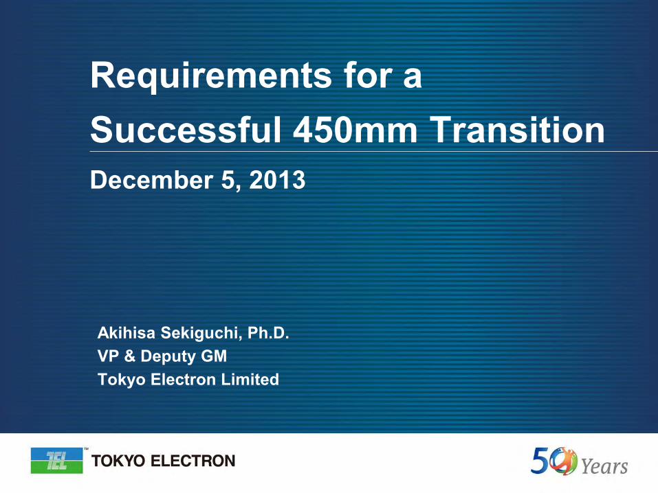
Requirements for a Successful 450mm Transition December 5, 2013
Akihisa Sekiguchi, Ph.D. VP & Deputy GM Tokyo Electron Limited

1 Akihisa Sekiguchi / Tokyo Electron/ December 5th, 2013
Outline
• Technology Development Requirements between now and the 450mm Era
• Recap of discussions to date
• TEL’s 450mm Development Status
• Summary
TEL is a trademark of Tokyo Electron Limited.
2 Akihisa Sekiguchi / Tokyo Electron/ December 5th, 2013
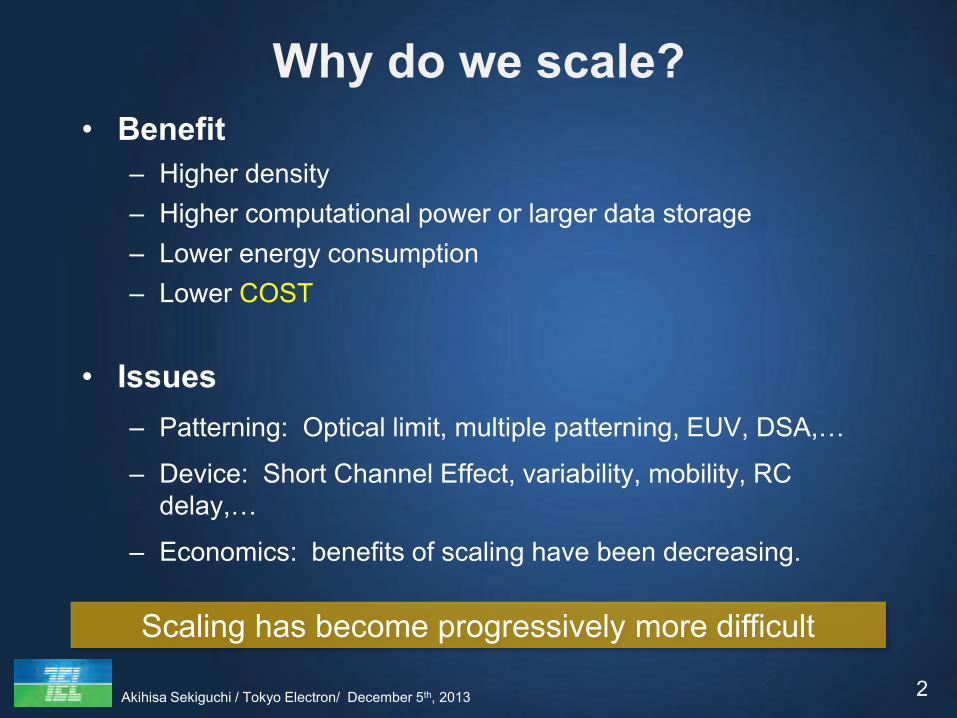
Why do we scale? • Benefit
– Higher density – Higher computational power or larger data storage – Lower energy consumption – Lower COST
• Issues – Patterning: Optical limit, multiple patterning, EUV, DSA,…
– Device: Short Channel Effect, variability, mobility, RC delay,…
– Economics: benefits of scaling have been decreasing.
Scaling has become progressively more difficult

3 Akihisa Sekiguchi / Tokyo Electron/ December 5th, 2013
Mor
e M
oore
Functional Diversification C
MO
S Sc
alin
g
New Material New Structure
Advanced Packaging (3DI / WLP)
3DI
Strained Si
High-k Metal Gate
Cu/ULK
FinFET
Lithography
ArF
ArF-Immersion
NIL, EBDW
More than Moore
Source :TEL based on ITRS
DP/MP
Now 2017~
SiGe / III-V
Flip-Chip 2.5D
Wire-Bonding
DRAM
NAND
STT-MRAM
3D NAND ReRAM
Emerging Memory
Ion Memory ZRAM…
450mm
DSA
Technical Challenges
EUV
Carbon Tr. /CNT
Difficult technical requirements on multiple fronts
Si Photonics
4 Akihisa Sekiguchi / Tokyo Electron/ December 5th, 2013
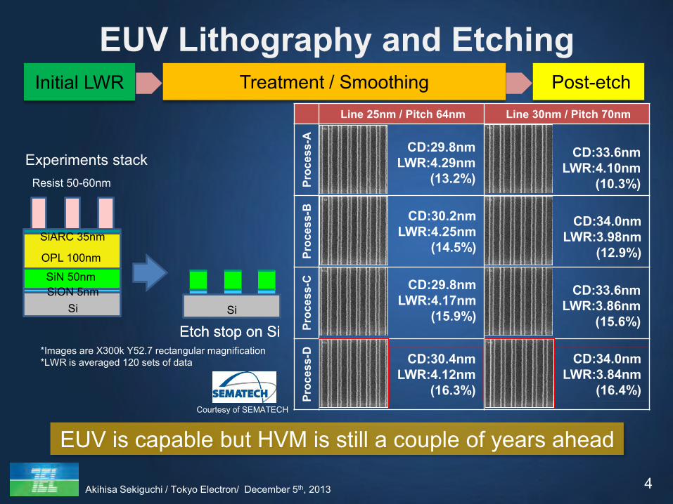
Initial LWR Treatment / Smoothing Post-etch
Experiments stack
Etch stop on Si
Line 25nm / Pitch 64nm Line 30nm / Pitch 70nm
Proc
ess-
A Pr
oces
s-B
Pr
oces
s-C
Pr
oces
s-D
CD:29.8nm LWR:4.29nm
(13.2%)
CD:30.2nm LWR:4.25nm
(14.5%)
CD:29.8nm LWR:4.17nm
(15.9%)
CD:30.4nm LWR:4.12nm
(16.3%)
CD:33.6nm LWR:4.10nm
(10.3%)
CD:34.0nm LWR:3.98nm
(12.9%)
CD:33.6nm LWR:3.86nm
(15.6%)
CD:34.0nm LWR:3.84nm
(16.4%)
*Images are X300k Y52.7 rectangular magnification *LWR is averaged 120 sets of data
EUV Lithography and Etching
Courtesy of SEMATECH
EUV is capable but HVM is still a couple of years ahead
Etch stop on Si Si
SiON 5nm SiN 50nm
OPL 100nm
SiARC 35nm
Resist 50-60nm
Si
5 Akihisa Sekiguchi / Tokyo Electron/ December 5th, 2013
Mor
e M
oore
Functional Diversification C
MO
S Sc
alin
g
New Material New Structure
Advanced Packaging (3DI / WLP)
3DI
Strained Si
High-k Metal Gate
Cu/ULK
FinFET
Lithography
ArF
ArF-Immersion
NIL, EBDW
More than Moore
Source :TEL based on ITRS
DP/MP
Now 2017~
SiGe / III-V
Flip-Chip 2.5D
Wire-Bonding
DRAM
NAND
STT-MRAM
3D NAND ReRAM
Emerging Memory
Ion Memory ZRAM…
450mm
DSA
Technical Challenges
EUV
Carbon Tr. /CNT
Difficult technical requirements on multiple fronts
Si Photonics
6 Akihisa Sekiguchi / Tokyo Electron/ December 5th, 2013
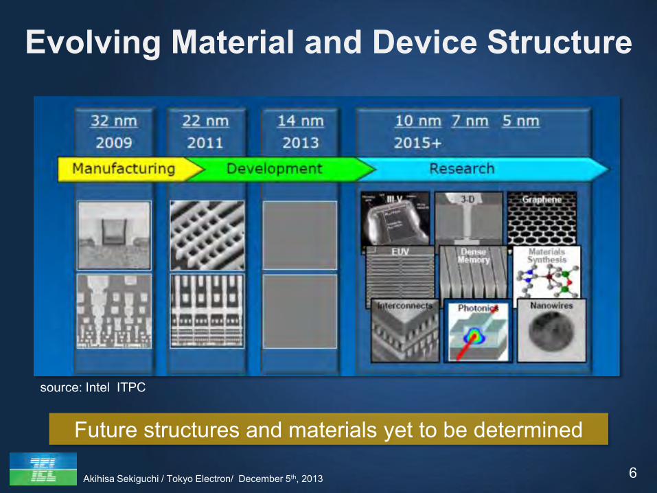
Evolving Material and Device Structure
source: Intel ITPC
Future structures and materials yet to be determined

7 Akihisa Sekiguchi / Tokyo Electron/ December 5th, 2013
Transistor with New Structures
Evolving structure complexities demand new processes
Planar MOSFET
Nanowire
FinFET
8 Akihisa Sekiguchi / Tokyo Electron/ December 5th, 2013
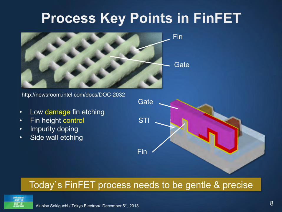
Process Key Points in FinFET
http://newsroom.intel.com/docs/DOC-2032
Fin
Gate
• Low damage fin etching • Fin height control • Impurity doping • Side wall etching
Fin
Gate
STI
Today`s FinFET process needs to be gentle & precise
9 Akihisa Sekiguchi / Tokyo Electron/ December 5th, 2013
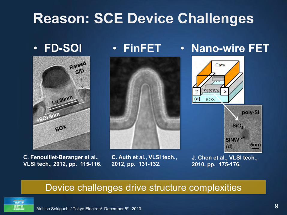
Reason: SCE Device Challenges
• FD-SOI
C. Fenouillet-Beranger et al., VLSI tech., 2012, pp. 115-116.
• FinFET • Nano-wire FET
C. Auth et al., VLSI tech., 2012, pp. 131-132.
J. Chen et al., VLSI tech., 2010, pp. 175-176.
Device challenges drive structure complexities

10 Akihisa Sekiguchi / Tokyo Electron/ December 5th, 2013
Reason for material change: Mobility
• Higher Performance via Mobility Enhancement • Stress effects, material changes are effective
T. Ghani, et al., IEDM2003, pp 978-980.
SiGe S/D Ge, III-V Channels
M. Radosavljevic, et al., IEDM2011, pp. 765-768.
Stress Liner
III-V materials are difficult to integrate
11 Akihisa Sekiguchi / Tokyo Electron/ December 5th, 2013
• Our development environment is extremely challenging
• Recap of discussions to date at Semicon
• TEL’s 450mm Development Status
• Summary
TEL is a trademark of Tokyo Electron Limited.

12 Akihisa Sekiguchi / Tokyo Electron/ December 5th, 2013
What have we discussed so far?
450mm Motivation
Successful Transition
Current Status
• Economic benefit of scaling has been decreasing • 450mm is the cost project for device maker
• Alignment, Collaboration and Cost sharing are key • Consortia such as G450C leads 450mm early
development
• Issues still remain regarding transition timing • We must remember past lessons & learn from our
mistakes
450mm motivation is simple, but no clear “exit strategy”

13 Akihisa Sekiguchi / Tokyo Electron/ December 5th, 2013
450mm Motivation
Ref. Nikon, 2013
450mm is a cost project (with Big Development)
Ref. TEL, 2012
14 Akihisa Sekiguchi / Tokyo Electron/ December 5th, 2013
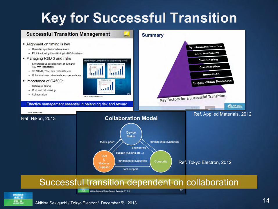
Key for Successful Transition
Ref. Nikon, 2013
Ref. Tokyo Electron, 2012
Ref. Applied Materials, 2012
Successful transition dependent on collaboration
15 Akihisa Sekiguchi / Tokyo Electron/ December 5th, 2013
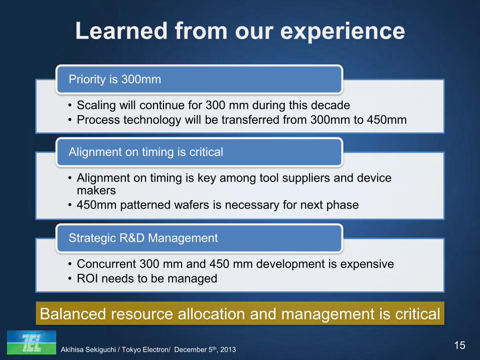
Learned from our experience
• Scaling will continue for 300 mm during this decade • Process technology will be transferred from 300mm to 450mm
Priority is 300mm
• Alignment on timing is key among tool suppliers and device makers
• 450mm patterned wafers is necessary for next phase
Alignment on timing is critical
• Concurrent 300 mm and 450 mm development is expensive • ROI needs to be managed
Strategic R&D Management
Balanced resource allocation and management is critical
16 Akihisa Sekiguchi / Tokyo Electron/ December 5th, 2013
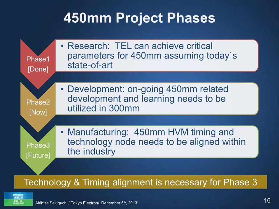
450mm Project Phases
Phase1 [Done]
• Research: TEL can achieve critical parameters for 450mm assuming today`s state-of-art
Phase2 [Now]
• Development: on-going 450mm related development and learning needs to be utilized in 300mm
Phase3 [Future]
• Manufacturing: 450mm HVM timing and technology node needs to be aligned within the industry
Technology & Timing alignment is necessary for Phase 3

17 Akihisa Sekiguchi / Tokyo Electron/ December 5th, 2013
Porting learning from 450 to 300mm
450mm activities needs to be utilized for 300mm
300mm
450mm Small Footprint
High Throughput Energy Saving Activity
Process Control Big Data Management
Maximizing shared components

18 Akihisa Sekiguchi / Tokyo Electron/ December 5th, 2013
Fab Ops: Sustainable Value Cycle
Resource-Saving Recipe
Peak Shift
Parts/Unit Management
Host
Lot/Wafer Dispatch
Resource Visualization
Recipe library
SEMI EESM SEMI S23
Tool suppliers will increasingly contribute to optimize operation
Data Mining

19 Akihisa Sekiguchi / Tokyo Electron/ December 5th, 2013
Equipment level: Chiller Energy Saving
Hose:15m
Chiller
Chiller
Sub Fab Area
Mezzanine
Hose:5m
Energy consumption can be reduced by about 20%
20 Akihisa Sekiguchi / Tokyo Electron/ December 5th, 2013
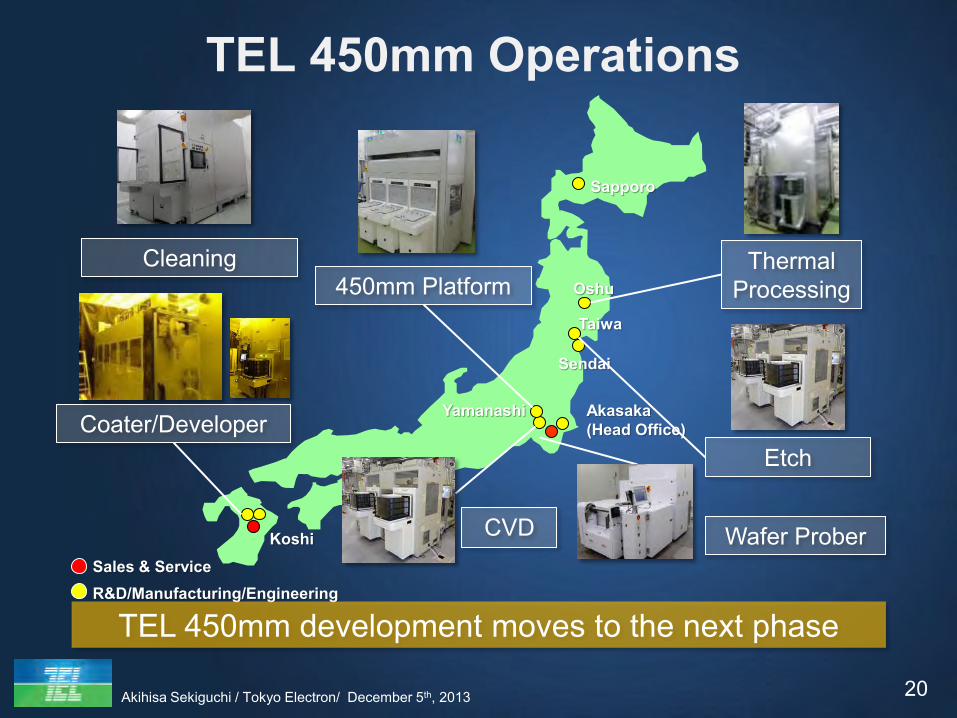
TEL 450mm Operations
Oshu
Sapporo
Yamanashi
Taiwa
Sendai
Akasaka (Head Office)
Koshi
Thermal Processing
Etch
Sales & Service R&D/Manufacturing/Engineering
450mm Platform Cleaning
Coater/Developer
TEL 450mm development moves to the next phase
Wafer Prober CVD

21 Akihisa Sekiguchi / Tokyo Electron/ December 5th, 2013
Open Platform Alliance Concept
Open Platform Alliance
Open Platform can benefit the supply chain
Parts Suppliers
Tool Suppliers
Device Makers
-Minimize part number -Increase productivity
-Develop tool with universal controller -Achieve asset light development
-Risk control by minimized parts & platform -Procurement, Maintenance, etc…
Semicon Japan 2012
22 Akihisa Sekiguchi / Tokyo Electron/ December 5th, 2013
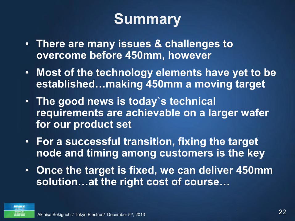
Summary • There are many issues & challenges to
overcome before 450mm, however • Most of the technology elements have yet to be
established…making 450mm a moving target • The good news is today`s technical
requirements are achievable on a larger wafer for our product set
• For a successful transition, fixing the target node and timing among customers is the key
• Once the target is fixed, we can deliver 450mm solution…at the right cost of course…

23 Akihisa Sekiguchi / Tokyo Electron/ December 5th, 2013
Thank you for listening