Embed Size (px)
Citation preview
G450C Status Supply Chain Collaboration on 450mm
Transition
SEMICON Europa October 9, 2013
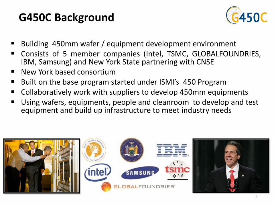
G450C Background
Building 450mm wafer / equipment development environment Consists of 5 member companies (Intel, TSMC, GLOBALFOUNDRIES,
IBM, Samsung) and New York State partnering with CNSE New York based consortium Built on the base program started under ISMI’s 450 Program Collaboratively work with suppliers to develop 450mm equipments Using wafers, equipments, people and cleanroom to develop and test
equipment and build up infrastructure to meet industry needs
2
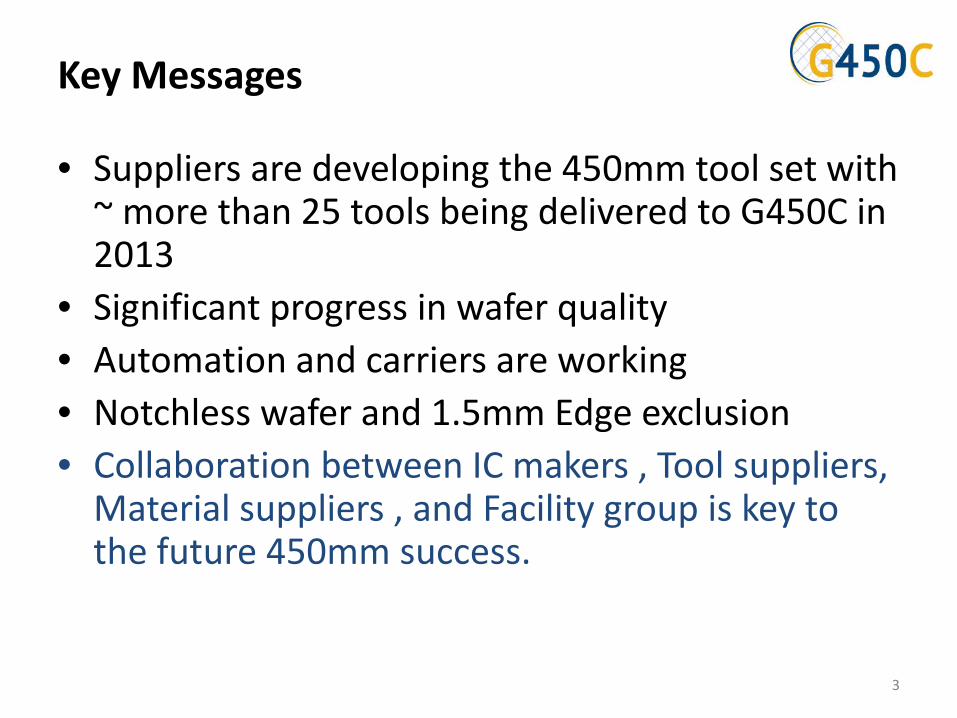
Key Messages
• Suppliers are developing the 450mm tool set with ~ more than 25 tools being delivered to G450C in 2013
• Significant progress in wafer quality • Automation and carriers are working • Notchless wafer and 1.5mm Edge exclusion • Collaboration between IC makers , Tool suppliers,
Material suppliers , and Facility group is key to the future 450mm success.
3
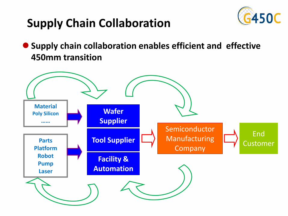
Supply Chain Collaboration
Supply chain collaboration enables efficient and effective 450mm transition
Wafer Supplier
Tool Supplier
Facility & Automation
Semiconductor Manufacturing
Company
End Customer Parts
Platform Robot Pump Laser
Material Poly Silicon
……
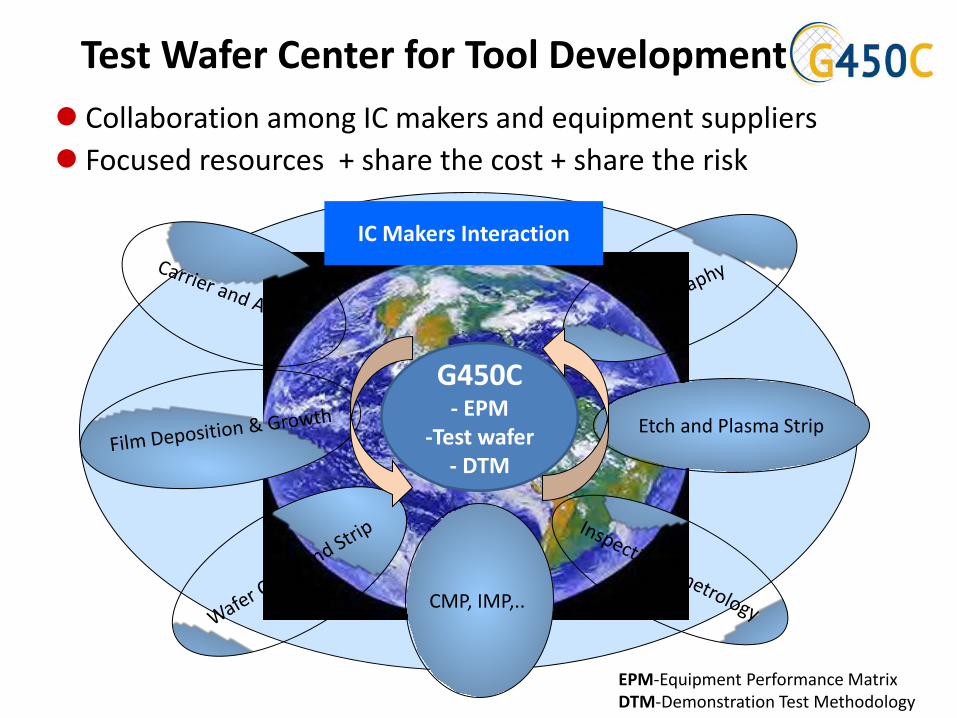
Test Wafer Center for Tool Development Collaboration among IC makers and equipment suppliers Focused resources + share the cost + share the risk
Etch and Plasma Strip
IC Makers Interaction
CMP, IMP,..
G450C - EPM
-Test wafer - DTM
EPM-Equipment Performance Matrix DTM-Demonstration Test Methodology

Development and Technology Intercept Targets
------ 2010 2011 2012 2013 2014 2015 2016
Early Development of Silicon and Infrastructure
G450C Program
ISMI 32/22nm Equipment Performance Metrics
10nm and beyond
Tools for Consortium Demonstrations (unit process)
Ready for IC Makers
Early 450mm Development
Test Wafers to support development and demo
14nm G450C Demonstrations
450mm and 300mm tools progress synchronously through technology generations
Full set of process and metrology, automation
Nominal “nm” = ITRS M1 Half Pitch
6
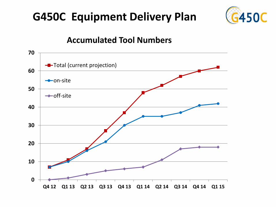
G450C Equipment Delivery Plan
Accumulated Tool Numbers
0
10
20
30
40
50
60
70
Q4 12 Q1 13 Q2 13 Q3 13 Q4 13 Q1 14 Q2 14 Q3 14 Q4 14 Q1 15
Total (current projection)
on-site
off-site
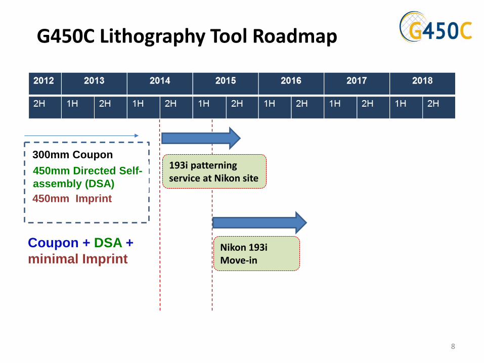
G450C Lithography Tool Roadmap
Coupon + DSA + minimal Imprint
450mm Imprint
300mm Coupon 450mm Directed Self-assembly (DSA)
193i patterning service at Nikon site
Nikon 193i Move-in
8
9
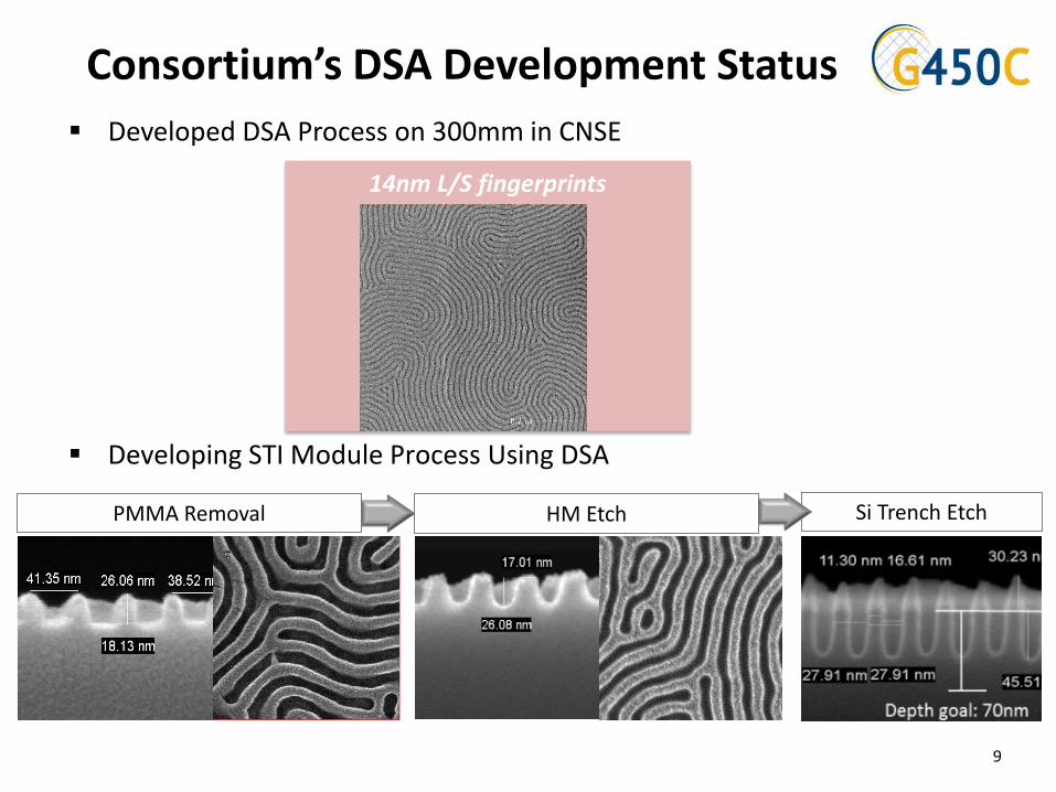
Consortium’s DSA Development Status
14nm L/S fingerprints
Developed DSA Process on 300mm in CNSE
PMMA Removal HM Etch Si Trench Etch
Developing STI Module Process Using DSA
Process Film 2013 1Q 2013 2Q 2013 3Q 2013 4Q 2014 1Q 2014 2Q
1 2 3 4 5 6 7 8 9 10 11 12 1 2 3 4 5 6
FEOL Oxide / Poly / SiN ★
Photo Resist ★
BEOL Metal
(Ni/TiN/W/TaN/Cu) ★
Lk film ★
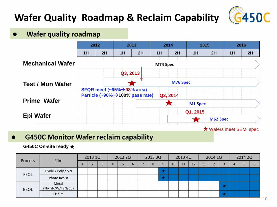
Wafer Quality Roadmap & Reclaim Capability
G450C On-site ready ★
Wafer quality roadmap
M74 Spec
M76 Spec
2012 2013 2014 2015 2016
1H 2H 1H 2H 1H 2H 1H 2H 1H 2H
M62 Spec
M1 Spec
Q2, 2014
Q1, 2015
Wafers meet SEMI spec
SFQR meet (~95%98% area) Particle (~90% 100% pass rate)
Q3, 2013
G450C Monitor Wafer reclaim capability
Mechanical Wafer
Test / Mon Wafer
Prime Wafer
Epi Wafer
10
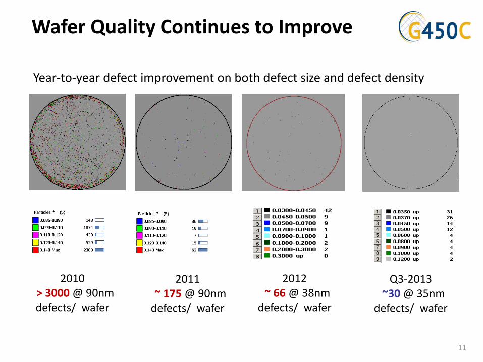
Wafer Quality Continues to Improve
Most recent ~ 66 @ 38nm sensitivity
2010 > 3000 @ 90nm defects/ wafer
Defects / Wafer Year-to-year defect improvement on both defect size and defect density
2011 ~ 175 @ 90nm defects/ wafer
Q3-2013 ~30 @ 35nm defects/ wafer
2012 ~ 66 @ 38nm defects/ wafer
11
12
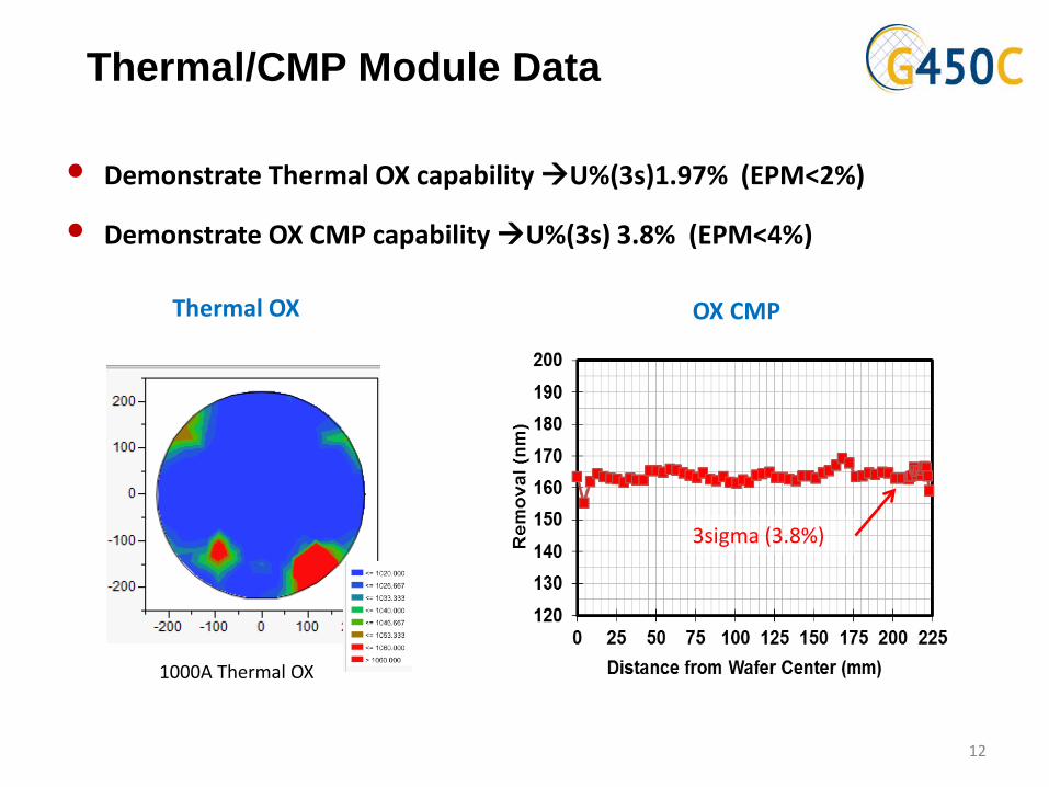
Thermal/CMP Module Data
• Demonstrate Thermal OX capability U%(3s)1.97% (EPM<2%)
• Demonstrate OX CMP capability U%(3s) 3.8% (EPM<4%)
OX CMP Thermal OX
1000A Thermal OX
3sigma (3.8%)
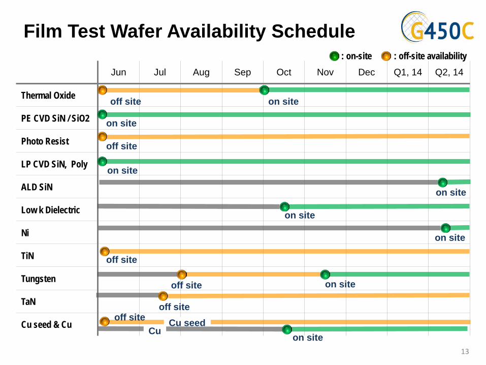
Film Test Wafer Availability Schedule
Jun Jul Aug Sep Oct Nov Dec Q1, 14 Q2, 14
Thermal Oxide
PE CVD SiN / SiO2
Photo Resist
LP CVD SiN, Poly
ALD SiN
Low k Dielectric
Ni
TiN
Tungsten
TaN
Cu seed & Cu
off site on site
on site
on site
on site
off site
off site on site
off site off site Cu seed
Cu on site
off site
: on-site : off-site availability
on site
on site
13
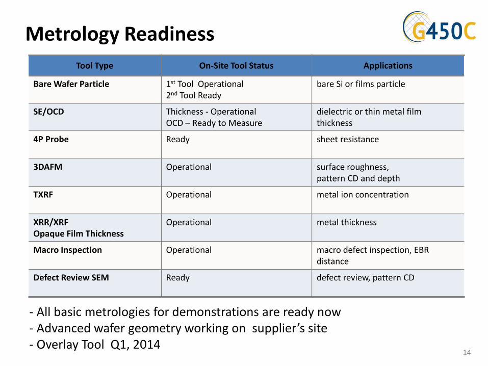
Metrology Readiness Tool Type On-Site Tool Status Applications
Bare Wafer Particle 1st Tool Operational 2nd Tool Ready
bare Si or films particle
SE/OCD Thickness - Operational OCD – Ready to Measure
dielectric or thin metal film thickness
4P Probe Ready
sheet resistance
3DAFM Operational
surface roughness, pattern CD and depth
TXRF Operational
metal ion concentration
XRR/XRF Opaque Film Thickness
Operational metal thickness
Macro Inspection Operational
macro defect inspection, EBR distance
Defect Review SEM Ready
defect review, pattern CD
- All basic metrologies for demonstrations are ready now - Advanced wafer geometry working on supplier’s site - Overlay Tool Q1, 2014
14
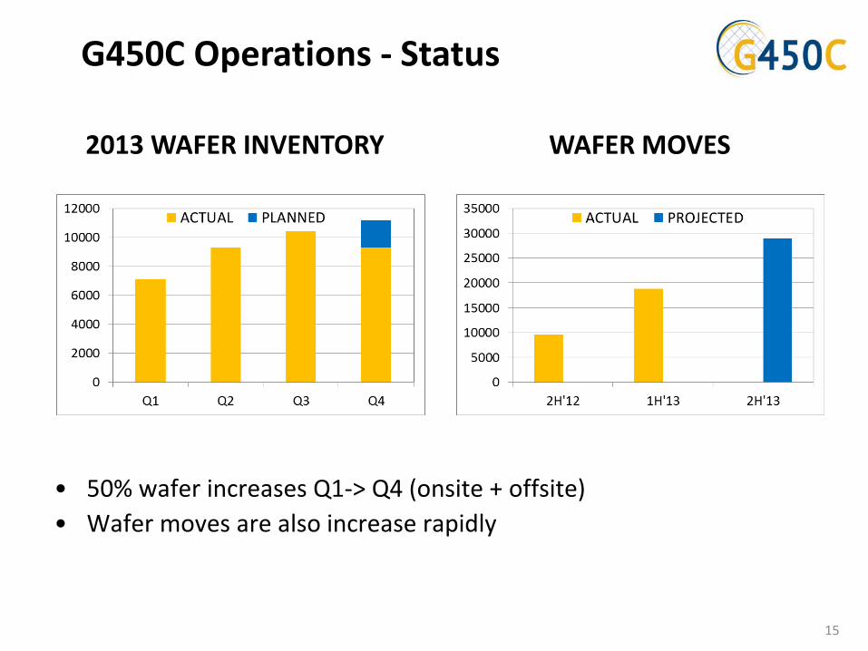
G450C Operations - Status
• 50% wafer increases Q1-> Q4 (onsite + offsite) • Wafer moves are also increase rapidly
15
WAFER MOVES 2013 WAFER INVENTORY
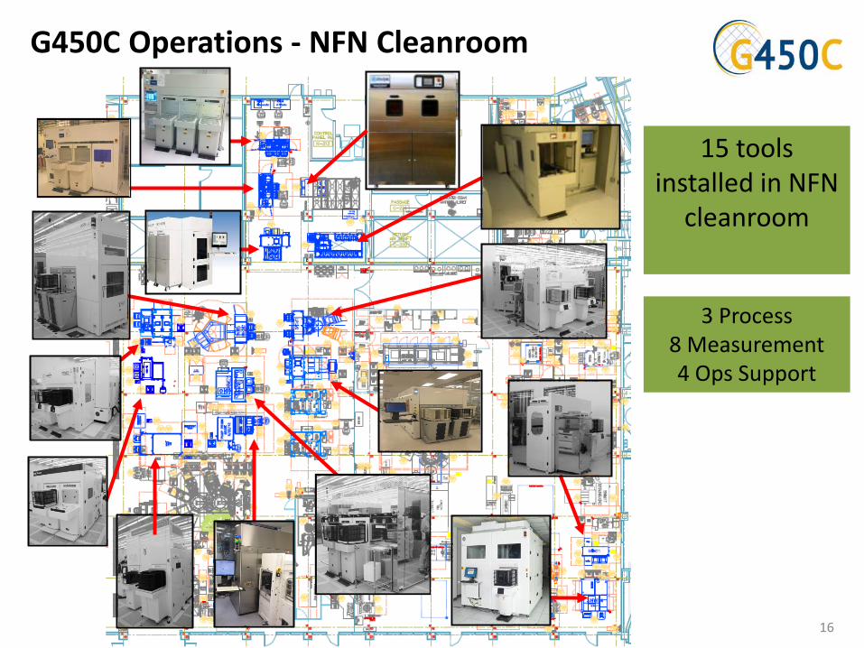
G450C Operations - NFN Cleanroom
15 tools installed in NFN
cleanroom
3 Process 8 Measurement 4 Ops Support
16
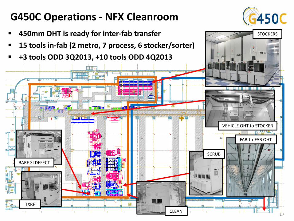
G450C Operations - NFX Cleanroom 450mm OHT is ready for inter-fab transfer 15 tools in-fab (2 metro, 7 process, 6 stocker/sorter) +3 tools ODD 3Q2013, +10 tools ODD 4Q2013
BARE SI DEFECT
TXRF
STOCKERS
FAB-to-FAB OHT
VEHICLE OHT to STOCKER
CLEAN
SCRUB
17
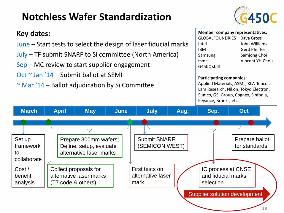
March April May June July Aug. Sep. Oct July Aug. Sep. Oct
Set up framework to collaborate
Collect proposals for alternative laser marks (T7 code & others)
Prepare 300mm wafers; Define, setup, evaluate alternative laser marks
First tests on alternative laser mark
Submit SNARF (SEMICON WEST)
Prepare ballot for standards
Cost / benefit analysis
IC process at CNSE and fiducial marks selection
Supplier solution development
Notchless Wafer Standardization Key dates: June – Start tests to select the design of laser fiducial marks July – TF submit SNARF to Si committee (North America) Sep – MC review to start supplier engagement Oct ~ Jan ’14 – Submit ballot at SEMI ~ Mar ‘14 – Ballot adjudication by Si Committee
18
Member company representatives: GLOBALFOUNDRIES Dave Gross Intel John Williams IBM Gerd Pfeiffer Samsung Samjong Choi tsmc Vincent YH Chou G450C staff Participating companies: Applied Materials, ASML, KLA-Tencor, Lam Research, Nikon, Tokyo Electron, Sumco, GSI Group, Cognex, Sinfonia, Keyance, Brooks, etc.
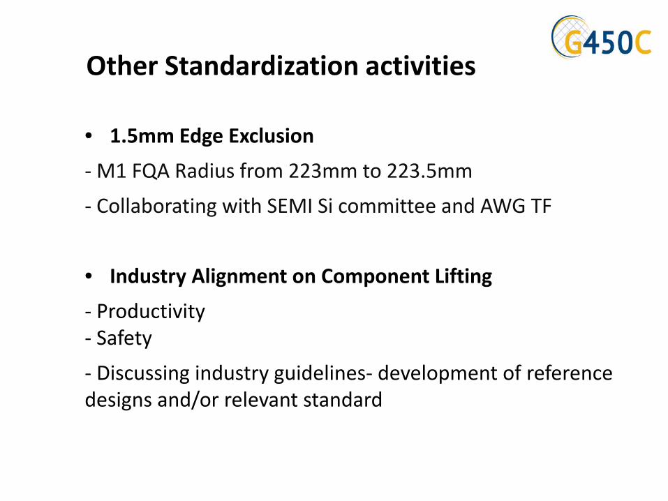
Other Standardization activities
• 1.5mm Edge Exclusion - M1 FQA Radius from 223mm to 223.5mm - Collaborating with SEMI Si committee and AWG TF
• Industry Alignment on Component Lifting - Productivity - Safety - Discussing industry guidelines- development of reference designs and/or relevant standard
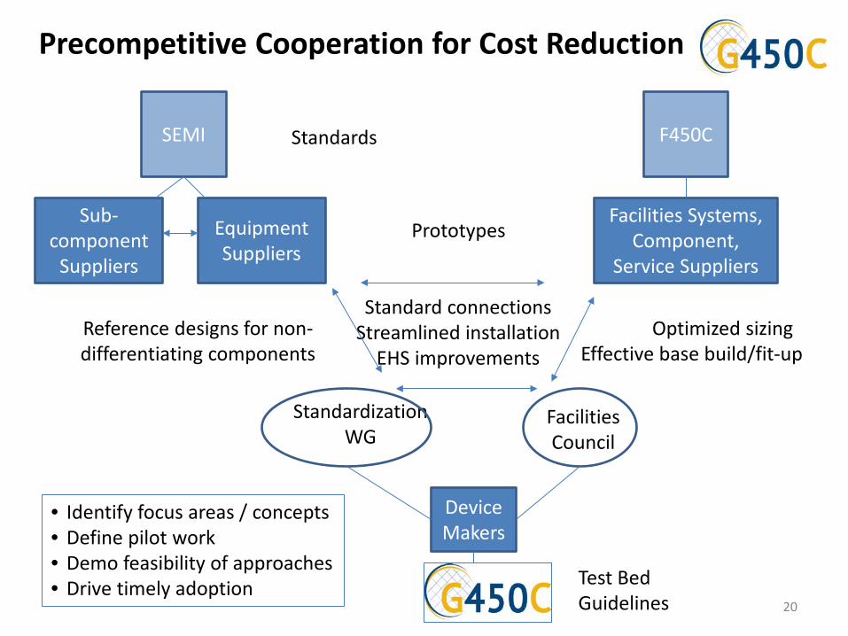
SEMI
Equipment Suppliers
Sub-component
Suppliers
F450C
Facilities Systems, Component,
Service Suppliers
Device Makers
Facilities Council
Standardization WG
Optimized sizing Effective base build/fit-up
Reference designs for non-differentiating components
Standard connections Streamlined installation
EHS improvements
Test Bed Guidelines
Standards
Prototypes
• Identify focus areas / concepts • Define pilot work • Demo feasibility of approaches • Drive timely adoption
Precompetitive Cooperation for Cost Reduction
20
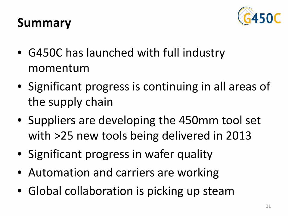
Summary
• G450C has launched with full industry momentum
• Significant progress is continuing in all areas of the supply chain
• Suppliers are developing the 450mm tool set with >25 new tools being delivered in 2013
• Significant progress in wafer quality • Automation and carriers are working • Global collaboration is picking up steam
21

Questions and Discussion