Embed Size (px)
Citation preview
Standard Form 298 (Rev 8/98) Prescribed by ANSI Std. Z39.18
Final Report
W911NF-12-1-0025
58398-EL-PCS.14
608-262-3863
a. REPORT
14. ABSTRACT
16. SECURITY CLASSIFICATION OF:
1. REPORT DATE (DD-MM-YYYY)
4. TITLE AND SUBTITLE
13. SUPPLEMENTARY NOTES
12. DISTRIBUTION AVAILIBILITY STATEMENT
6. AUTHORS
7. PERFORMING ORGANIZATION NAMES AND ADDRESSES
15. SUBJECT TERMS
b. ABSTRACT
2. REPORT TYPE
17. LIMITATION OF ABSTRACT
15. NUMBER OF PAGES
5d. PROJECT NUMBER
5e. TASK NUMBER
5f. WORK UNIT NUMBER
5c. PROGRAM ELEMENT NUMBER
5b. GRANT NUMBER
5a. CONTRACT NUMBER
Form Approved OMB NO. 0704-0188
3. DATES COVERED (From - To)-
Approved for public release; distribution is unlimited.
UU UU UU UU
08-01-2018 10-Jan-2012 9-Jan-2017
Final Report: Precision Controlled Carbon Materials for Next-Generation Optoelectronic & Photonic Devices
The views, opinions and/or findings contained in this report are those of the author(s) and should not contrued as an official Department of the Army position, policy or decision, unless so designated by other documentation.
9. SPONSORING/MONITORING AGENCY NAME(S) AND ADDRESS(ES)
U.S. Army Research Office P.O. Box 12211 Research Triangle Park, NC 27709-2211
REPORT DOCUMENTATION PAGE
11. SPONSOR/MONITOR'S REPORT NUMBER(S)
10. SPONSOR/MONITOR'S ACRONYM(S) ARO
8. PERFORMING ORGANIZATION REPORT NUMBER
19a. NAME OF RESPONSIBLE PERSON
19b. TELEPHONE NUMBERMichael Arnold
611103
c. THIS PAGE
The public reporting burden for this collection of information is estimated to average 1 hour per response, including the time for reviewing instructions, searching existing data sources, gathering and maintaining the data needed, and completing and reviewing the collection of information. Send comments regarding this burden estimate or any other aspect of this collection of information, including suggesstions for reducing this burden, to Washington Headquarters Services, Directorate for Information Operations and Reports, 1215 Jefferson Davis Highway, Suite 1204, Arlington VA, 22202-4302. Respondents should be aware that notwithstanding any other provision of law, no person shall be subject to any oenalty for failing to comply with a collection of information if it does not display a currently valid OMB control number.PLEASE DO NOT RETURN YOUR FORM TO THE ABOVE ADDRESS.
The Board of Regents of the University of Wisconsin SystemUniversity of Wisconsin - Madison 1.00
Suite 6401Madison, WI 53715 -1218
Agency Code:
Proposal Number: 58398ELPCS
Address: The Board of Regents of the University of Wisconsin Sys, Madison, WI 537151218 Country: USADUNS Number: 161202122 EIN: 396006492
Date Received: 08-Jan-2018Final Report for Period Beginning 10-Jan-2012 and Ending 09-Jan-2017
Begin Performance Period: 10-Jan-2012 End Performance Period: 09-Oct-2017
Submitted By: Michael ArnoldPhone: (608) 262-38630000
STEM Degrees: 3 STEM Participants: 7
RPPR Final Report as of 09-Jan-2018
Agreement Number: W911NF-12-1-0025
Organization: University of Wisconsin - Madison
Title: Precision Controlled Carbon Materials for Next-Generation Optoelectronic & Photonic Devices
Report Term: 0-OtherEmail: [email protected]
Distribution Statement: 1-Approved for public release; distribution is unlimited.
Major Goals: From original proposal:“Carbon nanotubes and graphene-based semiconducting materials exhibit exceptional properties and behaviors and unique physical phenomena that make them highly attractive for next-generation optoelectronic and photonic devices. Overall, in this project, we are building on our group’s unique abilities for creating precision-controlled carbon semiconductors and exploiting their exceptional characteristics to engineer next-generation carbon-based optoelectronic and photonic devices with superior performance and capabilities. These devices include carbon nanotube-based photovoltaic, photodetector, and light emitting devices, which build on our capabilities for creating highly monodisperse electronic-type-controlled and bandgap-controlled semiconducting nanotubes [1-3], as well as preliminary demonstrations of carbon nanotube donor/acceptor heterojunction diode devices in which the nanotubes are the light absorbers[3-7]. These devices also include semiconducting graphene optoelectronic and photonic devices, which build on our capabilities for creating structure-controlled nanopatterned graphene with tunable, semiconducting behavior and with refined edge structures [8-11]. Overall, work focuses on the study of materials’ optoelectronic and photophysical properties and new fundamental concepts in devices that exploit the exceptional properties of these nanocarbon materials.”
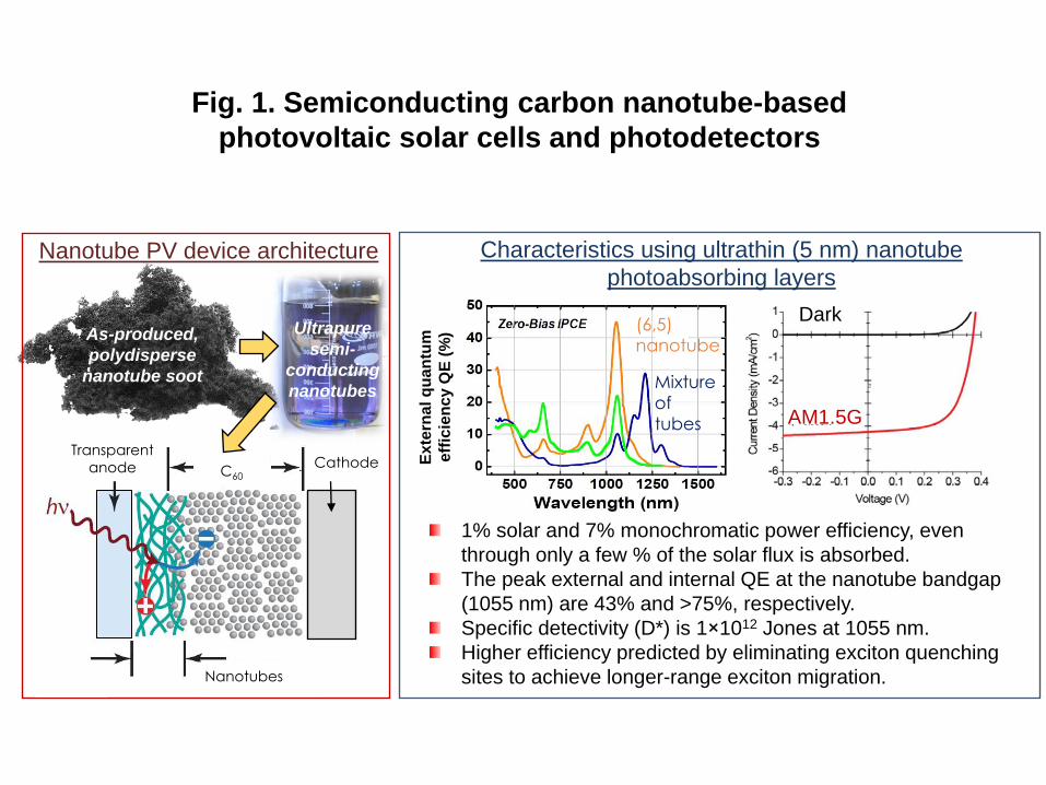
Accomplishments: In this project, we made breakthroughs in: (1) semiconducting carbon nanotube-based photovoltaic solar cells and photodetectors; (2) high-performance carbon nanotube electronics; (3) stretchable electronics; (4) nanostructured graphene plasmonics; and (5) polymer-nanotube conjugate chemistry. (1) Semiconducting carbon nanotube-based photovoltaic solar cells and photodetectorsSemiconducting carbon nanotubes are attractive absorbers for photovoltaic and photodetector devices. The use of nanotubes as light absorbers is distinct from other work which has used nanotubes as optically “dead” charge acceptors and collectors to other absorbers. Semiconducting nanotubes are strong, dye-like absorbers with bandgaps tunable to the ideal for single-junction solar PV ~1.3 eV or deeper into the IR for photodetectors. Nanotubes offer strong optical absorptivity (> 1E5 1/cm) and fast transport mobility (> 1E4 cm2/V/s). Compared to organic semiconductors, nanotubes are much more air stable. Other advantages include that nanotubes can be integrated onto arbitrary substrates, they are flexible, and they avoid complex heteroepitaxy. Prior to the project onset, we had discovered how to unlock nanotubes’ potential as photoabsorbers by pairing them with electron acceptors that overcome the ~0.2-0.3 eV exciton binding energy, including C60-fullerenes and derivatives, to form bilayered type-II donor/acceptor heterojunctions (Fig. 1).
Report Date: 09-Apr-2016
INVESTIGATOR(S):
Phone Number: 60826238630000Principal: Y
Name: Michael Scott Arnold Email: [email protected]
RPPR Final Report as of 09-Jan-2018
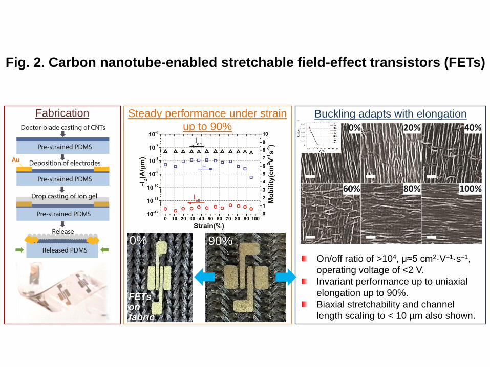
Support from this project resulted in:A) A review paper co-authored by Arnold et al. on nanotube-based photovoltaics (Phys. Chem. Chem. Phys. 2013). B) New insight into the factors affecting the efficiency of nanotube PV devices including:-i) Disruption of exciton transport by the polymer wrapper that surrounds each tube. Reducing the coverage of this polymer by 3x leads to a 2x improvement in device external quantum efficiency (EQE) – from 22 to 43% at bandgap (Chem. Phys. 2013).-ii) Sidewall and end defects induced by harsh processing methods that quench excitons. Replacing harsh processing methods (e.g., ultrasonication) with gentler methods (e.g., shear mixing) increases EQE from 28 to 49% (J. Phys. Chem. C. 2017; In Preparation 2017).-iii) Interfacial defect-mediated recombination. We have learned that loss occurs via trap-limited free carrier recombination using time-resolved microwave conductivity and low-temperature current-voltage measurements (Phys. Rev. B 2015; Submitted 2017).C) Advances in devices including:-i) Realization of 1% solar power efficiency and 7% monochromatic power efficiency in devices incorporating nanotubes films only 5 nn in thickness, despite the fact that only a few % of the solar flux is absorbed. The peak external and internal QE at the nanotube bandgap (1055 nm) are 43% and >75%, respectively (Appl. Phys. Lett. 2013).-ii) Demonstration of co-cast nanotube/fullerene blended heterojunction devices by using an aerogel infiltration technique, increasing the power conversion efficiency from 1.0 to 1.7% by increasing the interfacial area across which exciton-to-dissociated charge generation occurs (Small 2014).-iii) Realization of photodetectors with peak NIR specific detectivity (D*) of ~1E12 Jones at 1055 nm at 300K.High internal QE has been demonstrated for thin nanotube films in PV devices, which is promising. The internal QE drops for films thicker than > 10 nm due to the poor out-of-plane exciton diffusion length of ~5-10 nm, limiting external QE. Our models show that increasing this length to 100 nm (by making more pristine tubes with fewer defects) or improving the microstructure of nanotube/fullerene blends should result in dramatically more efficient PV devices (power efficiency >10%). The D* is already commercially relevant. Future optimization of detectors should proceed to understand factors that minimize dark current and maximize speed.(2) High-performance carbon nanotube electronicsIn research supported by multiple agencies, with crucial aspects supported by this award, we realized a major breakthrough in carbon nanotube electronics. We created for the first time field effect transistors (FETs) based on aligned arrays of nanotubes that outperform Si and GaAs FETs in terms of on-state current density and conductance. Conductance as high as 0.46 of the quantum conductance per nanotube was achieved. The conductance of the arrays reached 1.7 mS µm-1, which was 7x higher than previous nanotube array FETs made by other methods. The saturated on-state current density was as high as 900 µA µm-1, similar to or exceeding Si FETs compared at equivalent gate oxide thickness and off-state current density (ACS Nano 2014; Sci. Adv. 2016).(3) Stretchable electronicsTraditional electronic and optoelectronic devices fabricated on rigid substrates are usually brittle and undeformable. There is a growing demand for devices that can flex, stretch, and harmonize with the environment and humans. Most research in this area has focused on *flexible* electronics. Much more difficult is achieving devices that are not only flexible but highly *stretchable*, enabling large changes in shape and extreme changes in size. Support from this project resulted in (Fig. 2):A) The development of stretchable thin film transistors (TFTs) based on carbon nanotubes. Our initial architecture employed buckled thin films of polyfluorene-wrapped semiconducting single-walled carbon nanotubes as the TFT channel, buckled metal films as electrodes, and unbuckled flexible ion gel films as the dielectric. TFTs with this initial architecture are stretchable at up to 50% uniaxial elongation without degradation in performance (Nano Lett. 2014; U.S. Patent 8,987,707 2015).B) The development of buckled nanotube TFTs incorporating bucked ion gel gate dielectrics that are stretchable up to 90% uniaxial elongation (Appl. Phys. Lett. 2015).
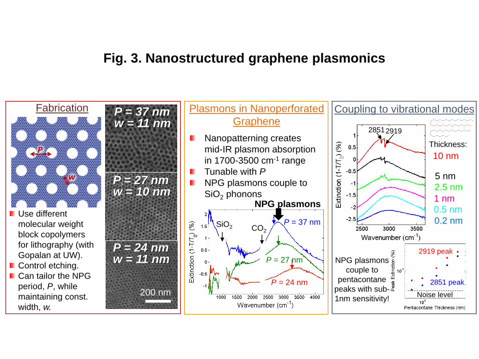
C) The development of buckled nanotube TFTs that are biaxially stretchable (J. Appl. Phys. 2017).D) The development of stretchable nanotube TFTs that can be down-scaled to sub-10 µm channel length – a length-scale of importance for future stretchable display technologies (In Preparation 2017).These TFTs are expected to facilitate unconventional applications in electronics and optoelectronics like implantable conformal biosensors, wearable electronic devices, and stretchable displays.(4) Nanostructured graphene plasmonics This project supported advances in the development of novel materials with mid-IR plasmon resonances (Fig. 3). We have shown that large-area sheets of graphene perforated by hexagonal periodic arrays of nm-scale holes with periods in the range of 24-120 nm support plasmon resonances in the range of 1700-3200 cm-1, with the resonance varying as P-0.5. These sheets can be easily fabricated using block copolymer lithography and have promise for optical biosensors because the plasmon can coupled with the vibrational modes of nearby molecules or molecules that pass through the perforations. The mid-IR absorption induced by the nanoscale patterning could also have function in IR modulation or emission applications (In Preparation, 2018).(5) Polymer-nanotube conjugate chemistryConjugated polymers can be exploited as agents for selectively wrapping and dispersing semiconducting versus metallic nanotubes. The mechanism is poorly understood. We have discovered that the primary factor governing semiconducting purity after sorting is the concentration of polymer in free solution as the tubes are wrapped during sonication. Our data indicate that at low polymer concentration, the resulting purity of semiconducting tubes may be as high as 99.999% (one metallic tube per 100,000) versus 66% prior to sorting (J. Phys. Chem. Lett. 2014). We have also collaborated with the lab of Padma Gopalan to develop an approach to remove polymer wrappers from nanotube surfaces (ACS Nano 2015) and to create polymer wrappers that are degradable and removable after thin film deposition (ACS Appl.
RPPR Final Report as of 09-Jan-2018
Training Opportunities: The graduate students and post-docs who have participated in this project have received technical training and gained meaningful practical experience with a variety of techniques including scanning electron microscopy, polymer wrapping of carbon nanotubes (ultrasonication, ultracentrifugation, solvent exchanges), floating evaporative self-assembly for aligning nanotubes, nanofabrication and electron beam lithography, field effect transistor fabrication and design, electrical transport measurements, optical absorption spectroscopy, plasmonics, knowledge of the photophysical properties of excitonic semiconductors, cleanroom processing, infrared spectroscopy, large dataset analysis using the software Matlab and Origin, and the thermal evaporation of metals and small molecule thin films, among other techniques. Presentations are given by researchers at individual or group meetings. Students learn project management, communication, and multitasking skills.
Results Dissemination: In addition to journal publications, our results were disseminated at 40 or more research presentations at major conferences, university seminars, and occasionally to corporations/industry.
RPPR Final Report as of 09-Jan-2018
Honors and Awards: * Arnold: Electrochemical Society (ECS) Nanocarbons Division Early Career Award (2018) * Note the ECS Nanocarbons division is the premier professional society entity in the field of nanocarbon materials research, having been formed in the beginning days of fullerene research in the early 1990's.* Arnold: U.S. runner-up in the U.S. Department of State ASPIRE Competition (2017)* Arnold: UW-Madison Romnes Faculty Fellowship (2017)* Arnold: Invited to and voted into: Executive Committee of the Nanocarbons Division of the Electrochemical Society (2016 – current)* Arnold: Honored Instructor Award, UW-Madison University Housing (2016)* Gerald Brady (Fellowship student): Best student presentation award at the Carbon 2016 Conference for his oral presentation entitled "High current per tube in carbon nanotube array field effect transistors" on research partially supported by this award. * Arnold: Harvey D. Spangler Faculty Fellowship, UW-Madison (2015)* Arnold: UW-Madison Vilas Associates Award (2015) * Arnold: National Science Foundation CAREER Award (2014)* Arnold: Center for Education Opportunity, UW-Madison, Dr. Brenda Pfaehler Award of Excellence (2013)* Arnold: American Chemical Society (ACS) Arthur K. Doolittle Award in Polymeric Materials Science and Engineering (2012) Note: Highly competitive & awarded to only 2 presenters per year at ACS.
Protocol Activity Status:
Technology Transfer: Arnold, M. S.; Xu, F., U.S. Patent No. 8,987,707: Stretchable transistors with buckled carbon nanotube films as conducting channels, Mar 24, 2015
PARTICIPANTS:
Person Months Worked: 5.00 Funding Support: Project Contribution: International Collaboration: International Travel: National Academy Member: N
Person Months Worked: 3.00 Funding Support: Project Contribution: International Collaboration: International Travel: National Academy Member: N
Person Months Worked: 15.00 Funding Support: Project Contribution:
Participant Type: PD/PIParticipant: Michael Person months = 5 months Arnold
Other Collaborators:
Participant Type: Postdoctoral (scholar, fellow or other postdoctoral position)Participant: Nathaniel Person months = 3 months Safron
Other Collaborators:
Participant Type: Graduate Student (research assistant)Participant: Matthew Person months = 54 months Shea
RPPR Final Report as of 09-Jan-2018
International Collaboration: International Travel: National Academy Member: N
Person Months Worked: 15.00 Funding Support: Project Contribution: International Collaboration: International Travel: National Academy Member: N
Person Months Worked: 2.00 Funding Support: Project Contribution: International Collaboration: International Travel: National Academy Member: N
Person Months Worked: 3.00 Funding Support: Project Contribution: International Collaboration: International Travel: National Academy Member: N
Person Months Worked: 12.00 Funding Support: Project Contribution: International Collaboration: International Travel: National Academy Member: N
Person Months Worked: 15.00 Funding Support: Project Contribution: International Collaboration: International Travel: National Academy Member: N
Person Months Worked: 4.00 Funding Support:
Other Collaborators:
Participant Type: Graduate Student (research assistant)Participant: Meng-Yin Person months = 19 months Wu
Other Collaborators:
Participant Type: Graduate Student (research assistant)Participant: Jialiang Person months = 2 months Wang
Other Collaborators:
Participant Type: Graduate Student (research assistant)Participant: Dominick Person months = 3 months Bindl
Other Collaborators:
Participant Type: Graduate Student (research assistant)Participant: Amir Person months = 12 months Mashal
Other Collaborators:
Participant Type: Graduate Student (research assistant)Participant: Chenghao Person months = 16 months Wan
Other Collaborators:
Participant Type: Postdoctoral (scholar, fellow or other postdoctoral position)Participant: Robert Person months = 4 months Jacobberger
RPPR Final Report as of 09-Jan-2018
Project Contribution: International Collaboration: International Travel: National Academy Member: N
Person Months Worked: 8.00 Funding Support: Project Contribution: International Collaboration: International Travel: National Academy Member: N
Person Months Worked: 5.00 Funding Support: Project Contribution: International Collaboration: International Travel: National Academy Member: N
Person Months Worked: 2.00 Funding Support: Project Contribution: International Collaboration: International Travel: National Academy Member: N
Person Months Worked: 2.00 Funding Support: Project Contribution: International Collaboration: International Travel: National Academy Member: N
Other Collaborators:
Participant Type: Postdoctoral (scholar, fellow or other postdoctoral position)Participant: Feng Person months = 8 months Xu
Other Collaborators:
Participant Type: Postdoctoral (scholar, fellow or other postdoctoral position)Participant: Naechul Person months = 5 months Shin
Other Collaborators:
Participant Type: Undergraduate StudentParticipant: Tou Person months = 2 months Chang
Other Collaborators:
Participant Type: Postdoctoral (scholar, fellow or other postdoctoral position)Participant: Yumin Person months = 2 months Ye
Other Collaborators:
ARTICLES:
RPPR Final Report as of 09-Jan-2018
Publication Identifier: 10.1016/j.chemphys.2012.08.001First Page #: 0Volume: 0
Date Submitted:
Authors:
Distribution Statement: 1-Approved for public release; distribution is unlimited.Acknowledged Federal Support:
Publication Identifier: 10.1063/1.4811359First Page #: 243101Volume: 102
Date Submitted:
Authors:
Distribution Statement: 1-Approved for public release; distribution is unlimited.Acknowledged Federal Support:
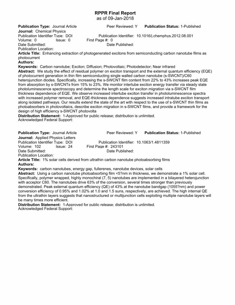
Publication Type: Journal ArticleJournal: Chemical Physics
Publication Location: Article Title: Enhancing extraction of photogenerated excitons from semiconducting carbon nanotube films as photocurrent
Keywords: Carbon nanotube; Exciton; Diffusion; Photovoltaic; Photodetector; Near infraredAbstract: We study the effect of residual polymer on exciton transport and the external quantum efficiency (EQE) of photocurrent generation in thin film semiconducting single walled carbon nanotube (s-SWCNT)/C60 heterojunction diodes. Specifically, increasing the s-SWCNT film content from 22% to 43% increases peak EQE from absorption by s-SWCNTs from 15% to 23%. We monitor intertube exciton energy transfer via steady state photoluminescence spectroscopy and determine the length scale for exciton migration via s-SWCNT film thickness dependence of EQE. We observe increased intertube exciton transfer in photoluminescence spectra with increased polymer removal, and EQE-thickness dependence suggests increased intratube exciton transport along isolated pathways. Our results extend the state of the art with respect to the use of s-SWCNT thin films as photoabsorbers in photovoltaics, describe exciton migration in s-SWCNT films, and provide a framework for the design of high efficiency s-SWCNT photovolta
Publication Type: Journal ArticleJournal: Applied Physics Letters
Publication Location: Article Title: 1% solar cells derived from ultrathin carbon nanotube photoabsorbing films
Keywords: carbon nanotubes, energy gap, fullerenes, nanotube devices, solar cellsAbstract: Using a carbon nanotube photoabsorbing film <5?nm in thickness, we demonstrate a 1% solar cell. Specifically, polymer wrapped, highly monochiral (7, 5) nanotubes are implemented in a bilayered heterojunction with acceptor C60. The nanotubes drive 63% of the conversion, several times stronger than previously demonstrated. Peak external quantum efficiency (QE) of 43% at the nanotube bandgap (1055?nm) and power conversion efficiency of 0.95% and 1.02% at 1.0 and 1.5 suns, respectively, are achieved. The high internal QE from the ultrathin layers suggests that nanostructured or multijunction cells exploiting multiple nanotube layers will be many times more efficient.
Publication Identifier Type: DOIIssue: 0
Date Published:
Publication Identifier Type: DOIIssue: 24
Date Published:
Peer Reviewed: Y
Peer Reviewed: Y
Publication Status: 1-Published
Publication Status: 1-Published
RPPR Final Report as of 09-Jan-2018
Publication Identifier: 10.1039/c3cp52752bFirst Page #: 14896Volume: 15
Date Submitted:
Authors:
Distribution Statement: 1-Approved for public release; distribution is unlimited.Acknowledged Federal Support:
Publication Identifier: 10.1002/smll.201400696First Page #: 3299Volume: 10
Date Submitted:
Authors:
Distribution Statement: 1-Approved for public release; distribution is unlimited.Acknowledged Federal Support:
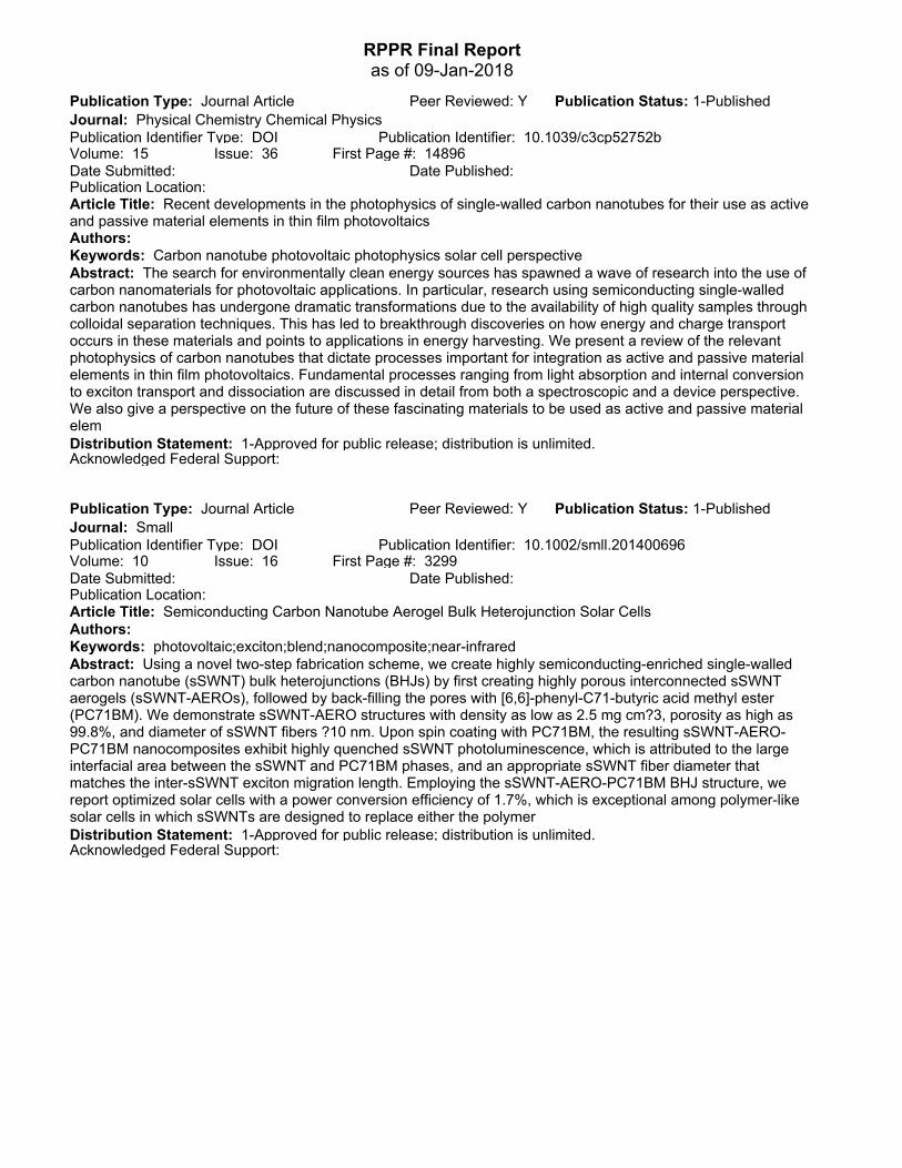
Publication Type: Journal ArticleJournal: Physical Chemistry Chemical Physics
Publication Location: Article Title: Recent developments in the photophysics of single-walled carbon nanotubes for their use as active and passive material elements in thin film photovoltaics
Keywords: Carbon nanotube photovoltaic photophysics solar cell perspectiveAbstract: The search for environmentally clean energy sources has spawned a wave of research into the use of carbon nanomaterials for photovoltaic applications. In particular, research using semiconducting single-walled carbon nanotubes has undergone dramatic transformations due to the availability of high quality samples through colloidal separation techniques. This has led to breakthrough discoveries on how energy and charge transport occurs in these materials and points to applications in energy harvesting. We present a review of the relevant photophysics of carbon nanotubes that dictate processes important for integration as active and passive material elements in thin film photovoltaics. Fundamental processes ranging from light absorption and internal conversion to exciton transport and dissociation are discussed in detail from both a spectroscopic and a device perspective. We also give a perspective on the future of these fascinating materials to be used as active and passive material elem
Publication Type: Journal ArticleJournal: Small
Publication Location: Article Title: Semiconducting Carbon Nanotube Aerogel Bulk Heterojunction Solar Cells
Keywords: photovoltaic;exciton;blend;nanocomposite;near-infraredAbstract: Using a novel two-step fabrication scheme, we create highly semiconducting-enriched single-walled carbon nanotube (sSWNT) bulk heterojunctions (BHJs) by first creating highly porous interconnected sSWNT aerogels (sSWNT-AEROs), followed by back-filling the pores with [6,6]-phenyl-C71-butyric acid methyl ester (PC71BM). We demonstrate sSWNT-AERO structures with density as low as 2.5 mg cm?3, porosity as high as 99.8%, and diameter of sSWNT fibers ?10 nm. Upon spin coating with PC71BM, the resulting sSWNT-AERO-PC71BM nanocomposites exhibit highly quenched sSWNT photoluminescence, which is attributed to the large interfacial area between the sSWNT and PC71BM phases, and an appropriate sSWNT fiber diameter that matches the inter-sSWNT exciton migration length. Employing the sSWNT-AERO-PC71BM BHJ structure, we report optimized solar cells with a power conversion efficiency of 1.7%, which is exceptional among polymer-like solar cells in which sSWNTs are designed to replace either the polymer
Publication Identifier Type: DOIIssue: 36
Date Published:
Publication Identifier Type: DOIIssue: 16
Date Published:
Peer Reviewed: Y
Peer Reviewed: Y
Publication Status: 1-Published
Publication Status: 1-Published
RPPR Final Report as of 09-Jan-2018
Publication Identifier: 10.1021/nl403941aFirst Page #: 682Volume: 14
Date Submitted:
Authors:
Distribution Statement: 1-Approved for public release; distribution is unlimited.Acknowledged Federal Support:
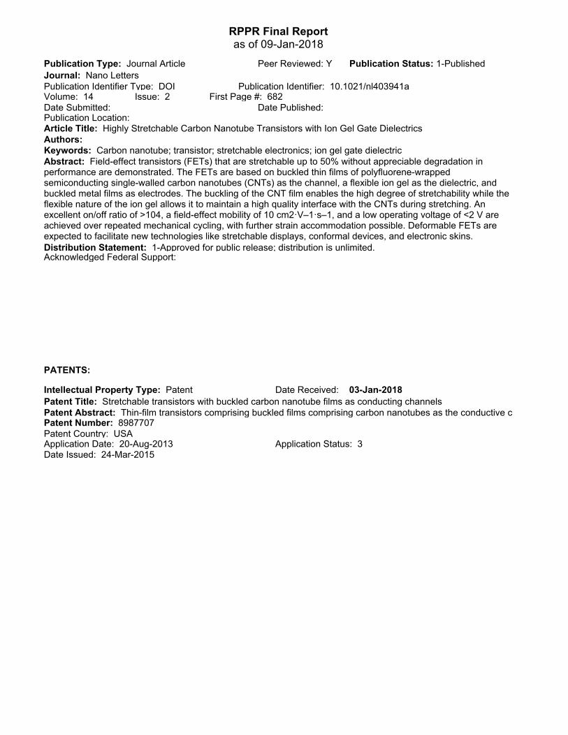
Publication Type: Journal ArticleJournal: Nano Letters
Publication Location: Article Title: Highly Stretchable Carbon Nanotube Transistors with Ion Gel Gate Dielectrics
Keywords: Carbon nanotube; transistor; stretchable electronics; ion gel gate dielectricAbstract: Field-effect transistors (FETs) that are stretchable up to 50% without appreciable degradation in performance are demonstrated. The FETs are based on buckled thin films of polyfluorene-wrapped semiconducting single-walled carbon nanotubes (CNTs) as the channel, a flexible ion gel as the dielectric, and buckled metal films as electrodes. The buckling of the CNT film enables the high degree of stretchability while the flexible nature of the ion gel allows it to maintain a high quality interface with the CNTs during stretching. An excellent on/off ratio of >104, a field-effect mobility of 10 cm2·V–1·s–1, and a low operating voltage of <2 V are achieved over repeated mechanical cycling, with further strain accommodation possible. Deformable FETs are expected to facilitate new technologies like stretchable displays, conformal devices, and electronic skins.
Publication Identifier Type: DOIIssue: 2
Date Published:
Peer Reviewed: Y Publication Status: 1-Published
PATENTS:
Date Received: 03-Jan-2018
Patent Abstract: Thin-film transistors comprising buckled films comprising carbon nanotubes as the conductive channel are provided. Also provided are methods of fabricating the transistors. The transistors, which are highly stretchable and bendable, exhibit stable performance even when operated under high tensile strains.Patent Number: 8987707Patent Country: USA
Date Issued: 24-Mar-2015
Patent Title: Stretchable transistors with buckled carbon nanotube films as conducting channels
Application Date: 20-Aug-2013 Application Status: 3
Intellectual Property Type: Patent
CathodeTransparent
anode
Ultrapure
semi-
conducting
nanotubes
As-produced,
polydisperse
nanotube soot
Nanotube PV device architecture
C60
Nanotubes
Characteristics using ultrathin (5 nm) nanotube
photoabsorbing layers
AM1.5G
Dark(6,5)
nanotube
Mixture
of
tubes
1% solar and 7% monochromatic power efficiency, even
through only a few % of the solar flux is absorbed.
The peak external and internal QE at the nanotube bandgap
(1055 nm) are 43% and >75%, respectively.
Specific detectivity (D*) is 1×10¹² Jones at 1055 nm.
Higher efficiency predicted by eliminating exciton quenching
sites to achieve longer-range exciton migration.
Exte
rna
l q
ua
ntu
m
eff
icie
ncy Q
E (
%)
Fig. 1. Semiconducting carbon nanotube-based
photovoltaic solar cells and photodetectors
On/off ratio of >104, µ≈5 cm2·V–1·s–1,
operating voltage of <2 V.
Invariant performance up to uniaxial
elongation up to 90%.
Biaxial stretchability and channel
length scaling to < 10 µm also shown.
Fabrication Buckling adapts with elongationSteady performance under strain
up to 90%
Au
0% 90%
FETson fabric
Fig. 2. Carbon nanotube-enabled stretchable field-effect transistors (FETs)
Nanopatterning creates
mid-IR plasmon absorption
in 1700-3500 cm-1 range
Tunable with P
NPG plasmons couple to
SiO2 phonons
Fabrication Plasmons in Nanoperforated
Graphene
200 nm
10 nm
5 nm
2.5 nm
1 nm0.5 nm
0.2 nm
2919 peak
2851 peak
Thickness:
P = 24 nm
P = 37 nm
P = 27 nm
CO2SiO2
28512919
NPG plasmons
couple to
pentacontane
peaks with sub-
1nm sensitivity!
Use different
molecular weight
block copolymers
for lithography (with
Gopalan at UW).
Control etching.
Can tailor the NPG
period, P, while
maintaining const.
width, w.
Noise level
P = 37 nmw = 11 nm
P = 27 nmw = 10 nm
P = 24 nmw = 11 nm
NPG plasmons
Fig. 3. Nanostructured graphene plasmonics
Coupling to vibrational modes