Embed Size (px)
Citation preview
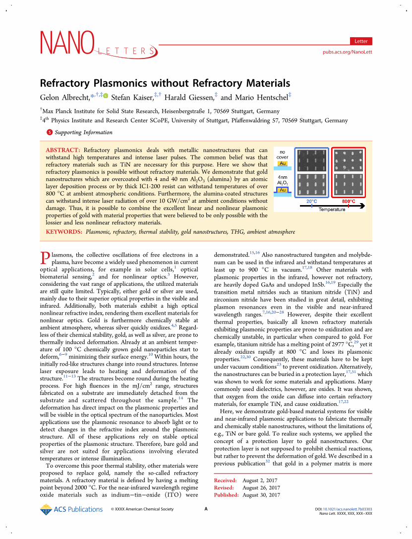
Refractory Plasmonics without Refractory MaterialsGelon Albrecht,*,†,‡ Stefan Kaiser,‡,† Harald Giessen,‡ and Mario Hentschel‡
†Max Planck Institute for Solid State Research, Heisenbergstraße 1, 70569 Stuttgart, Germany‡4th Physics Institute and Research Center SCoPE, University of Stuttgart, Pfaffenwaldring 57, 70569 Stuttgart, Germany
*S Supporting Information
ABSTRACT: Refractory plasmonics deals with metallic nanostructures that canwithstand high temperatures and intense laser pulses. The common belief was thatrefractory materials such as TiN are necessary for this purpose. Here we show thatrefractory plasmonics is possible without refractory materials. We demonstrate that goldnanostructures which are overcoated with 4 and 40 nm Al2O3 (alumina) by an atomiclayer deposition process or by thick IC1-200 resist can withstand temperatures of over800 °C at ambient atmospheric conditions. Furthermore, the alumina-coated structurescan withstand intense laser radiation of over 10 GW/cm2 at ambient conditions withoutdamage. Thus, it is possible to combine the excellent linear and nonlinear plasmonicproperties of gold with material properties that were believed to be only possible with thelossier and less nonlinear refractory materials.
KEYWORDS: Plasmonic, refractory, thermal stability, gold nanostructures, THG, ambient atmosphere
Plasmons, the collective oscillations of free electrons in aplasma, have become a widely used phenomenon in current
optical applications, for example in solar cells,1 opticalbiomaterial sensing,2 and for nonlinear optics.3 However,considering the vast range of applications, the utilized materialsare still quite limited. Typically, either gold or silver are used,mainly due to their superior optical properties in the visible andinfrared. Additionally, both materials exhibit a high opticalnonlinear refractive index, rendering them excellent materials fornonlinear optics. Gold is furthermore chemically stable atambient atmosphere, whereas silver quickly oxidizes.4,5 Regard-less of their chemical stability, gold, as well as silver, are prone tothermally induced deformation. Already at an ambient temper-ature of 100 °C chemically grown gold nanoparticles start todeform,6−9 minimizing their surface energy.10 Within hours, theinitially rod-like structures change into round structures. Intenselaser exposure leads to heating and deformation of thestructure.11−13 The structures become round during the heatingprocess. For high fluences in the mJ/cm2 range, structuresfabricated on a substrate are immediately detached from thesubstrate and scattered throughout the sample.14 Thedeformation has direct impact on the plasmonic properties andwill be visible in the optical spectrum of the nanoparticles. Mostapplications use the plasmonic resonance to absorb light or todetect changes in the refractive index around the plasmonicstructure. All of these applications rely on stable opticalproperties of the plasmonic structure. Therefore, bare gold andsilver are not suited for applications involving elevatedtemperatures or intense illumination.To overcome this poor thermal stability, other materials were
proposed to replace gold, namely the so-called refractorymaterials. A refractory material is defined by having a meltingpoint beyond 2000 °C. For the near-infrared wavelength regimeoxide materials such as indium−tin−oxide (ITO) were
demonstrated.15,16 Also nanostructured tungsten and molybde-num can be used in the infrared and withstand temperatures atleast up to 900 °C in vacuum.17,18 Other materials withplasmonic properties in the infrared, however not refractory,are heavily doped GaAs and undoped InSb.16,19 Especially thetransition metal nitrides such as titanium nitride (TiN) andzirconium nitride have been studied in great detail, exhibitingplasmon resonances even in the visible and near-infraredwavelength ranges.7,16,20−28 However, despite their excellentthermal properties, basically all known refractory materialsexhibiting plasmonic properties are prone to oxidization and arechemically unstable, in particular when compared to gold. Forexample, titanium nitride has a melting point of 2977 °C,29 yet italready oxidizes rapidly at 800 °C and loses its plasmonicproperties.22,30 Consequently, these materials have to be keptunder vacuum conditions23 to prevent oxidization. Alternatively,the nanostructures can be buried in a protection layer,17,31 whichwas shown to work for some materials and applications. Manycommonly used dielectrics, however, are oxides. It was shown,that oxygen from the oxide can diffuse into certain refractorymaterials, for example TiN, and cause oxidization.17,22
Here, we demonstrate gold-based material systems for visibleand near-infrared plasmonic applications to fabricate thermallyand chemically stable nanostructures, without the limitations of,e.g., TiN or bare gold. To realize such systems, we applied theconcept of a protection layer to gold nanostructures. Ourprotection layer is not supposed to prohibit chemical reactions,but rather to prevent the deformation of gold. We described in aprevious publication32 that gold in a polymer matrix is more
Received: August 2, 2017Revised: August 26, 2017Published: August 30, 2017
Letter
pubs.acs.org/NanoLett
© XXXX American Chemical Society A DOI: 10.1021/acs.nanolett.7b03303Nano Lett. XXXX, XXX, XXX−XXX
stable upon laser exposure. The general idea of this concept hasbeen widely used for many years.33−36 While these publicationsreport first strong indications of the benefits of cover layers, nosystematic study of the temperature nor of the thicknessdependence have been performed. Both quantities are offundamental as well as of practical importance. For example,thickly covered structures are not useful for plasmonic sensingtype experiments. Thus, we significantly extent the previouslyreported results by studying the temperature evolution fromroom temperature up to 1100 °C, well above the gold meltingtemperature. We also show that already thin cover layerssignificantly stabilize the structures. What is more, wedemonstrate the superior performance of the covered structuresupon intense laser illumination, also highly important for variousapplications.Besides the cover material, also the substrate material
influences the stability of the nanostructures.37,38 Therefore,we compared Suprasil and Al2O3 as substrate materials. As covermaterial, we choose Al2O3 and IC1-200, a polysiloxane-basedspin-on dielectric material, used for multilayer lithography. Al2O3is a refractory material; however, it is a dielectric material anddoes not exhibit plasmon resonances. It is deposited by atomiclayer deposition and forms an amorphous film (alumina). TheAl2O3 substrate is commercially available sapphire glass. Asummary of all material systems is shown in Figure 1. In all
further figures the pictographs introduced in this figure are usedto indicate the corresponding material system. We have chosenthe materials for two reasons: IC1-200 can be easily applied viaspin-coating and is thus a cheap and straightforward way to coateven complex nanostructures. Atomic layer deposition ofalumina is known to produce dense and crack-free films ofwell-controllable thickness. The material itself is expected to beextremely stable, while the defect-free layers also allow forultimately thin, yet closed films. For such thin films of 4 nmthickness, the plasmonic near-field of the structure stillsignificantly extends into the volume above the cover layer andthus allows for interaction with it for, e.g., sensing applications.
For the fabrication of the gold rod arrays, standard electronbeam lithography is used. The metals are deposited on theSuprasil and sapphire substrates by thermal evaporation. Thethicknesses are 2 nm chromium as the adhesion layer and 40 nmgold on top (see Figure 1). The chromium adhesion layer has amajor effect on the stability of the gold structures39 leading to animproved adhesion to the substrate and therefore increaseddimensional stability. The width of the rods is chosen to be 60nm. Their length is varied from 140 to 320 nm. All opticalmeasurements are performed with light polarized parallel to thelong rod axis. The lattice constant is 500 nm for both directions.The total area of one array is 80 μm × 80 μm. Scanning electronmicrographs are shown in Figure 2. More SEM images areavailable in the Supporting Information. All structures arecleaned after the chemical lift-off by 20 s of oxygen plasmatreatment. The IC1-200 coating is deposited by spin-coating(4000 rpm for 40s) and afterward annealed at 200 °C for 1 min.Finally, the film thickness was determined to be 150 nm for all ofthese samples by a stylus profiler. For the atomic layer depositionof Al2O3 (Cambridge NanoTech Savannah 100) trimethyl-aluminium (TMA) and water are used as precursor gases. Thesample is heated to 250 °C during the process, resulting in agrowth rate around 0.1 nm per cycle.TiN nanostructures show strong oxidization at 800 °C, even in
an argon-flushed environment.22 Therefore, as a first test for ourproposed material systems, all covered and uncovered structuresare exposed to 800 °C in ambient atmosphere to investigate theperformance in comparison to TiN. The transmission spectra aremeasured with a commercial FTIR setup after preparation andafter 1, 4, and 8 h exposed to 800 °C in air. The spectral data froma silicon detector and an InGaAs detector are stitched together,making it possible to measure the wavelength range from 600 to1600 nm. First, the spectral evolution for the different materialsystems are compared for structures with a resonance around1000 nm. Due to the different refractive indices of thesurrounding, the length thus varies for different covers. Thesize dependence is discussed later and is depicted in Figure 5.The optical transmission spectra for the bare gold rods are
shown in the upper left panel of Figure 2. The upper right panelscontain SEM micrographs of the rods before exposure to heatand after 8 h at 800 °C. The initially 220 nm long rods havestrongly deformed to a circular shape, in agreement withliterature.6 The deformation leads to a shrinking along theoptically excited direction. This is reflected in the more than 300nm shift of the center wavelength to lower wavelengths.Furthermore, the resonance is rather broad for gold at therespective wavelength. This can be attributed to the veryinhomogeneous sizes of the deformed particles. Further SEMmicrographs with a wider angle of view are provided in theSupporting Information.In comparison, the rods coated with 4 nm alumina are still
intact. The spectra show only a minor shift of the centerwavelength toward shorter wavelengths and a small decrease inthe full width at half-maximum (fwhm) of the resonance.The third panel displays the 40 nm thick alumina-coated rods.
The coating also protects the nanostructure from deformation. Asmall shift occurs, but toward longer wavelengths. A red shiftcould occur by an elongation of the nanostructures; however, thisis unlikely. Alternatively the effective refractive index of thesurrounding could change. This may occur due to a kind ofsintering effect of the alumina. Another possibility is theformation of a thin gold-alumina intergranular film.40 However,as the effect is not visible in case of a thin alumina coating, the
Figure 1. Geometrical parameters used for the rod nanostructures andthe applied covers. In the bottom, visualization of degradation sources,which we applied to determine the damage threshold of our structures.The alumina-coated gold structures withstand heating up to 900 °C inambient atmosphere, where bare gold rods or TiN rods are alreadydestroyed. Furthermore, the alumina-covered gold rods show a stableoptical third harmonic generation at 10GW/cm2 laser intensity, wherebare gold rods already show strong degradation of the third harmonicsignal.
Nano Letters Letter
DOI: 10.1021/acs.nanolett.7b03303Nano Lett. XXXX, XXX, XXX−XXX
B
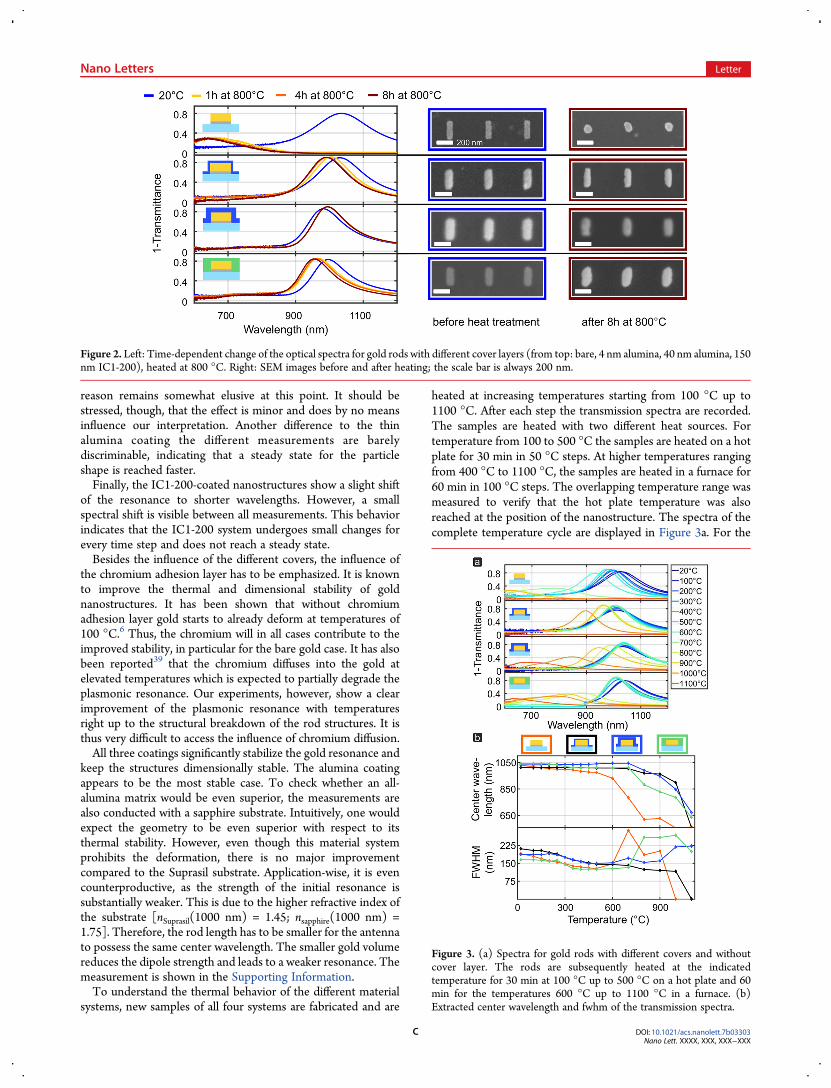
reason remains somewhat elusive at this point. It should bestressed, though, that the effect is minor and does by no meansinfluence our interpretation. Another difference to the thinalumina coating the different measurements are barelydiscriminable, indicating that a steady state for the particleshape is reached faster.Finally, the IC1-200-coated nanostructures show a slight shift
of the resonance to shorter wavelengths. However, a smallspectral shift is visible between all measurements. This behaviorindicates that the IC1-200 system undergoes small changes forevery time step and does not reach a steady state.Besides the influence of the different covers, the influence of
the chromium adhesion layer has to be emphasized. It is knownto improve the thermal and dimensional stability of goldnanostructures. It has been shown that without chromiumadhesion layer gold starts to already deform at temperatures of100 °C.6 Thus, the chromium will in all cases contribute to theimproved stability, in particular for the bare gold case. It has alsobeen reported39 that the chromium diffuses into the gold atelevated temperatures which is expected to partially degrade theplasmonic resonance. Our experiments, however, show a clearimprovement of the plasmonic resonance with temperaturesright up to the structural breakdown of the rod structures. It isthus very difficult to access the influence of chromium diffusion.All three coatings significantly stabilize the gold resonance and
keep the structures dimensionally stable. The alumina coatingappears to be the most stable case. To check whether an all-alumina matrix would be even superior, the measurements arealso conducted with a sapphire substrate. Intuitively, one wouldexpect the geometry to be even superior with respect to itsthermal stability. However, even though this material systemprohibits the deformation, there is no major improvementcompared to the Suprasil substrate. Application-wise, it is evencounterproductive, as the strength of the initial resonance issubstantially weaker. This is due to the higher refractive index ofthe substrate [nSuprasil(1000 nm) = 1.45; nsapphire(1000 nm) =1.75]. Therefore, the rod length has to be smaller for the antennato possess the same center wavelength. The smaller gold volumereduces the dipole strength and leads to a weaker resonance. Themeasurement is shown in the Supporting Information.To understand the thermal behavior of the different material
systems, new samples of all four systems are fabricated and are
heated at increasing temperatures starting from 100 °C up to1100 °C. After each step the transmission spectra are recorded.The samples are heated with two different heat sources. Fortemperature from 100 to 500 °C the samples are heated on a hotplate for 30 min in 50 °C steps. At higher temperatures rangingfrom 400 °C to 1100 °C, the samples are heated in a furnace for60 min in 100 °C steps. The overlapping temperature range wasmeasured to verify that the hot plate temperature was alsoreached at the position of the nanostructure. The spectra of thecomplete temperature cycle are displayed in Figure 3a. For the
Figure 2. Left: Time-dependent change of the optical spectra for gold rods with different cover layers (from top: bare, 4 nm alumina, 40 nm alumina, 150nm IC1-200), heated at 800 °C. Right: SEM images before and after heating; the scale bar is always 200 nm.
Figure 3. (a) Spectra for gold rods with different covers and withoutcover layer. The rods are subsequently heated at the indicatedtemperature for 30 min at 100 °C up to 500 °C on a hot plate and 60min for the temperatures 600 °C up to 1100 °C in a furnace. (b)Extracted center wavelength and fwhm of the transmission spectra.
Nano Letters Letter
DOI: 10.1021/acs.nanolett.7b03303Nano Lett. XXXX, XXX, XXX−XXX
C
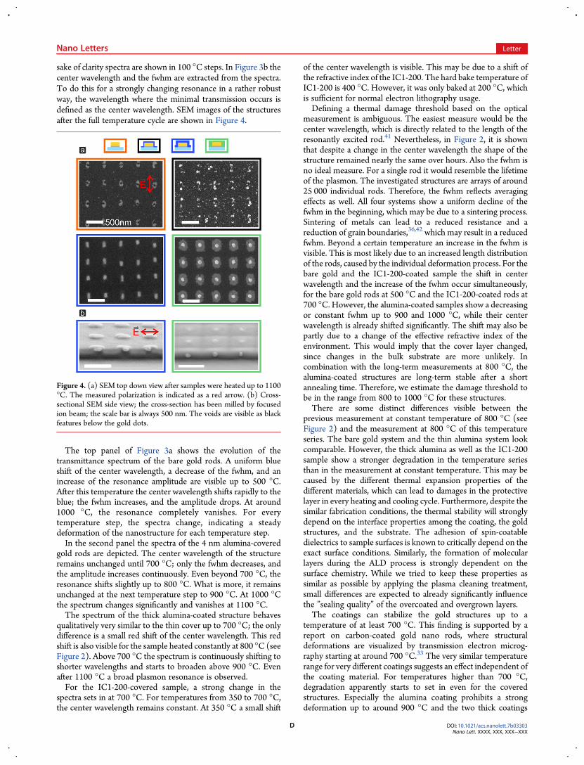
sake of clarity spectra are shown in 100 °C steps. In Figure 3b thecenter wavelength and the fwhm are extracted from the spectra.To do this for a strongly changing resonance in a rather robustway, the wavelength where the minimal transmission occurs isdefined as the center wavelength. SEM images of the structuresafter the full temperature cycle are shown in Figure 4.
The top panel of Figure 3a shows the evolution of thetransmittance spectrum of the bare gold rods. A uniform blueshift of the center wavelength, a decrease of the fwhm, and anincrease of the resonance amplitude are visible up to 500 °C.After this temperature the center wavelength shifts rapidly to theblue; the fwhm increases, and the amplitude drops. At around1000 °C, the resonance completely vanishes. For everytemperature step, the spectra change, indicating a steadydeformation of the nanostructure for each temperature step.In the second panel the spectra of the 4 nm alumina-covered
gold rods are depicted. The center wavelength of the structureremains unchanged until 700 °C; only the fwhm decreases, andthe amplitude increases continuously. Even beyond 700 °C, theresonance shifts slightly up to 800 °C. What is more, it remainsunchanged at the next temperature step to 900 °C. At 1000 °Cthe spectrum changes significantly and vanishes at 1100 °C.The spectrum of the thick alumina-coated structure behaves
qualitatively very similar to the thin cover up to 700 °C; the onlydifference is a small red shift of the center wavelength. This redshift is also visible for the sample heated constantly at 800 °C (seeFigure 2). Above 700 °C the spectrum is continuously shifting toshorter wavelengths and starts to broaden above 900 °C. Evenafter 1100 °C a broad plasmon resonance is observed.For the IC1-200-covered sample, a strong change in the
spectra sets in at 700 °C. For temperatures from 350 to 700 °C,the center wavelength remains constant. At 350 °C a small shift
of the center wavelength is visible. This may be due to a shift ofthe refractive index of the IC1-200. The hard bake temperature ofIC1-200 is 400 °C. However, it was only baked at 200 °C, whichis sufficient for normal electron lithography usage.Defining a thermal damage threshold based on the optical
measurement is ambiguous. The easiest measure would be thecenter wavelength, which is directly related to the length of theresonantly excited rod.41 Nevertheless, in Figure 2, it is shownthat despite a change in the center wavelength the shape of thestructure remained nearly the same over hours. Also the fwhm isno ideal measure. For a single rod it would resemble the lifetimeof the plasmon. The investigated structures are arrays of around25 000 individual rods. Therefore, the fwhm reflects averagingeffects as well. All four systems show a uniform decline of thefwhm in the beginning, which may be due to a sintering process.Sintering of metals can lead to a reduced resistance and areduction of grain boundaries,36,42 which may result in a reducedfwhm. Beyond a certain temperature an increase in the fwhm isvisible. This is most likely due to an increased length distributionof the rods, caused by the individual deformation process. For thebare gold and the IC1-200-coated sample the shift in centerwavelength and the increase of the fwhm occur simultaneously,for the bare gold rods at 500 °C and the IC1-200-coated rods at700 °C. However, the alumina-coated samples show a decreasingor constant fwhm up to 900 and 1000 °C, while their centerwavelength is already shifted significantly. The shift may also bepartly due to a change of the effective refractive index of theenvironment. This would imply that the cover layer changed,since changes in the bulk substrate are more unlikely. Incombination with the long-term measurements at 800 °C, thealumina-coated structures are long-term stable after a shortannealing time. Therefore, we estimate the damage threshold tobe in the range from 800 to 1000 °C for these structures.There are some distinct differences visible between the
previous measurement at constant temperature of 800 °C (seeFigure 2) and the measurement at 800 °C of this temperatureseries. The bare gold system and the thin alumina system lookcomparable. However, the thick alumina as well as the IC1-200sample show a stronger degradation in the temperature seriesthan in the measurement at constant temperature. This may becaused by the different thermal expansion properties of thedifferent materials, which can lead to damages in the protectivelayer in every heating and cooling cycle. Furthermore, despite thesimilar fabrication conditions, the thermal stability will stronglydepend on the interface properties among the coating, the goldstructures, and the substrate. The adhesion of spin-coatabledielectrics to sample surfaces is known to critically depend on theexact surface conditions. Similarly, the formation of molecularlayers during the ALD process is strongly dependent on thesurface chemistry. While we tried to keep these properties assimilar as possible by applying the plasma cleaning treatment,small differences are expected to already significantly influencethe ”sealing quality” of the overcoated and overgrown layers.The coatings can stabilize the gold structures up to a
temperature of at least 700 °C. This finding is supported by areport on carbon-coated gold nano rods, where structuraldeformations are visualized by transmission electron microg-raphy starting at around 700 °C.33 The very similar temperaturerange for very different coatings suggests an effect independent ofthe coating material. For temperatures higher than 700 °C,degradation apparently starts to set in even for the coveredstructures. Especially the alumina coating prohibits a strongdeformation up to around 900 °C and the two thick coatings
Figure 4. (a) SEM top down view after samples were heated up to 1100°C. The measured polarization is indicated as a red arrow. (b) Cross-sectional SEM side view; the cross-section has been milled by focusedion beam; the scale bar is always 500 nm. The voids are visible as blackfeatures below the gold dots.
Nano Letters Letter
DOI: 10.1021/acs.nanolett.7b03303Nano Lett. XXXX, XXX, XXX−XXX
D
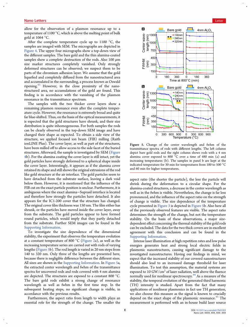
allow for the observation of a plasmon resonance up to atemperature of 1100 °C, which is above the melting point of bulkgold at 1064 °C.After the complete temperature cycle up to 1100 °C, the
samples are imaged with SEM. The micrographs are depicted inFigure 4. The upper four micrographs show a top-down view ofthe different samples. The bare gold and the thin alumina-coatedsamples show a complete destruction of the rods. Also 100 μmsize marker structures completely vanished. Only stronglydeformed structures can be observed; we suspect them to beparts of the chromium adhesion layer. We assume that the goldliquefied and completely diffused from the nanostructured areaand accumulated in the surrounding, a process known as Oswaldripening.43 However, in the close proximity of the nano-structured area, no accumulations of the gold are found. Thisfinding is in accordance with the vanishing of the plasmonresonance in the transmittance spectrum.The samples with the two thicker cover layers show a
remaining plasmon resonance even after the complete temper-ature cycle. However, the resonance is extremely broad and quitefar blue-shifted. Thus, on the basis of the optical measurements, itis expected that the gold structures have shrunk, and their sizedistribution is quite inhomogeneous. For both samples the rodscan be clearly observed in the top-down SEM image and havechanged their shape as expected. To obtain a side view of thestructure, we applied focused ion beam (FIB) milling (RaithionLINE Plus). The cover layer, as well as part of the structures,have been milled off to allow access to the side facet of the buriedstructures. Afterward, the sample is investigated by SEM (Figure4b). For the alumina coating the cover layer is still intact, yet thegold particles have strongly deformed to a spherical shape insidethe cover layer. Interestingly, it appears as if the alumina coverretained its shape and still shows the original extrusions of the rodlike gold structure at the air interface. The gold particles seem tohave detached from the substrate surface, leaving a dark voidbelow them. However, it is mentioned that the influence of theFIB cut on the exact particle position is unclear. Furthermore, it isambiguous where the exact alumina−Suprasil interface is locatedand therefore how strongly the particles have detached. It alsoappears for the IC1-200 cover that the structure has changed.The original cover film thickness was 150 nm. The film either hasshrunk, or the particles have moved inside the cover layer, awayfrom the substrate. The gold particles appear to have formedround particles, which would imply that they partly detachedfrom the substrate. Further SEM images can be found in theSupporting Information.To investigate the size dependence of the dimensional
stability, the experiment that observes the temperature evolutionat a constant temperature of 800 °C (Figure 2a), as well as theincreasing temperature series are carried out with rods of varyinglengths (Figure 5b). The rod length is varied in 20 nm steps from140 to 320 nm. Only three of the lengths are presented here,because there is negligible difference between the different sizes.All sizes are shown in the Supporting Information. In Figure 5a,the extracted center wavelength and fwhm of the transmittancespectra for uncovered rods and rods covered with 4 nm aluminaare depicted. The structures are exposed to a constant 800 °C.The bare gold rods exhibit a strong change of resonancewavelength as well as fwhm in the first time step. In thesubsequent heating steps, no significant change is visible, inaccordance with the previous results.Furthermore, the aspect ratio from length to width plays an
essential role for the strength of the change. The smaller the
aspect ratio (the shorter the particle), the less the particle willshrink during the deformation to a circular shape. For thealumina-coated structures, a decrease in the center wavelength aswell as in the fwhm is visible. Nevertheless, the change is far lesspronounced, and the influence of the aspect ratio on the strengthof change is visible. The size dependence of the temperaturecycle presented in Figure 3 is depicted in Figure 5b. Also here allof the previously observed features are visible. The aspect ratiodetermines the strength of the change, but not the temperaturestability. On the basis of these observations, a major size-dependent effect concerning the thermal stability of the gold rodscan be excluded. The data for the two thick covers are in excellentagreement with this conclusion and can be found in theSupporting Information.Intense laser illumination at high repetition rates and low pulse
energies generates heat and strong local electric fields inplasmonic nanostructures, causing significant damage to theinvestigated nanostructures. Having our findings in mind, weexpect that the increased stability of our covered nanostructuresshould also lead to an increased damage threshold for laserillumination. To test this assumption, the material systems areexposed to 10 GW/cm2 of laser radiation, well above the fluencenormally used for nonlinear spectroscopy.44 As a measure of thestability, the temporal evolution of the generated third harmonic(TH) intensity is studied. Apart from the fact that manyapplications of nonlinear plasmonics in fact use TH generation,we also choose this measure as the signal is known to cruciallydepend on the exact shape of the plasmonic resonance.45 Themeasurement is performed with an in-house build laser source
Figure 5. Change of the center wavelength and fwhm of thetransmittance spectra of rods with different lengths. The left columndepict bare gold rods and the right column shows rods with a 4 nmalumina cover exposed to 800 °C over a time of 480 min (a) andincreasing temperatures (b). The samples in panel b are kept at theindicated temperature for 30 min for temperatures from 100 to 500 °Cand 60 min for higher temperatures.
Nano Letters Letter
DOI: 10.1021/acs.nanolett.7b03303Nano Lett. XXXX, XXX, XXX−XXX
E
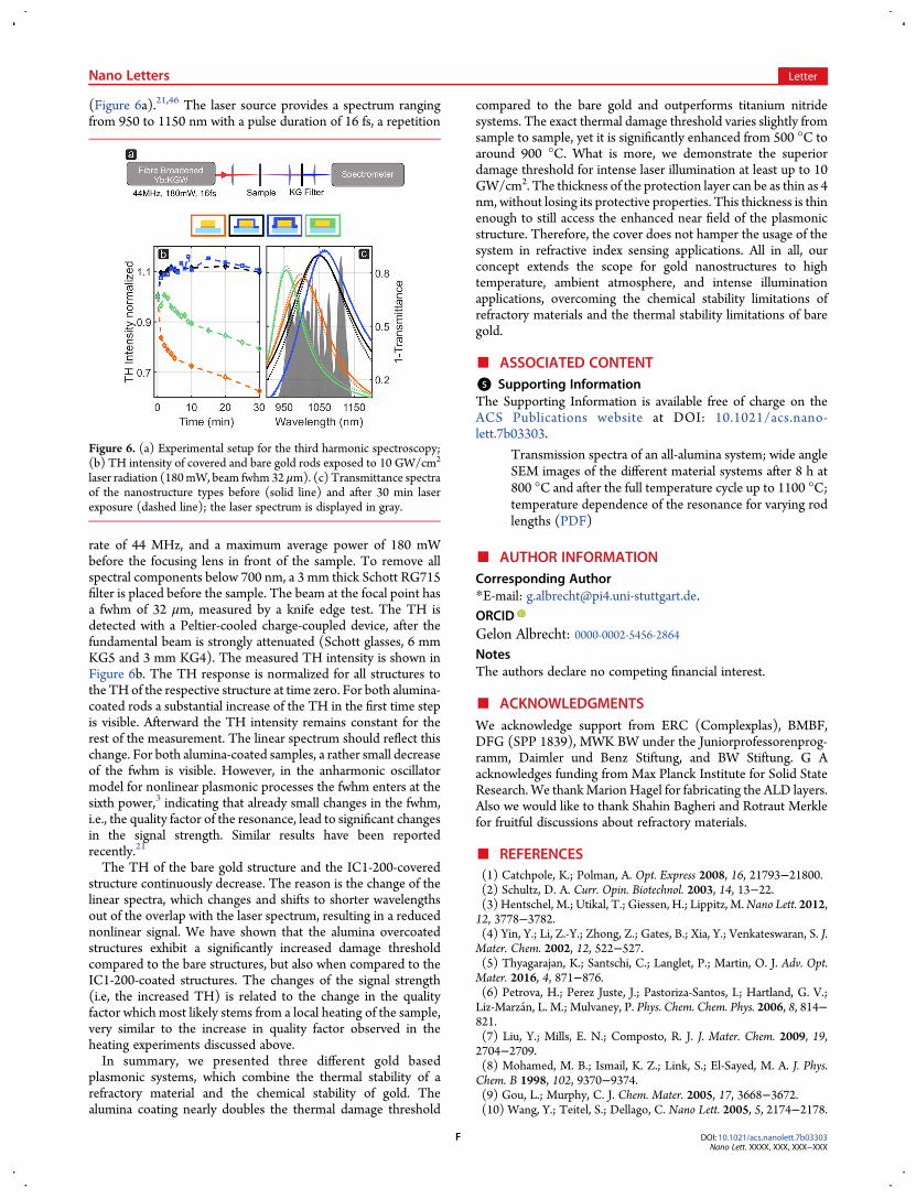
(Figure 6a).21,46 The laser source provides a spectrum rangingfrom 950 to 1150 nm with a pulse duration of 16 fs, a repetition
rate of 44 MHz, and a maximum average power of 180 mWbefore the focusing lens in front of the sample. To remove allspectral components below 700 nm, a 3 mm thick Schott RG715filter is placed before the sample. The beam at the focal point hasa fwhm of 32 μm, measured by a knife edge test. The TH isdetected with a Peltier-cooled charge-coupled device, after thefundamental beam is strongly attenuated (Schott glasses, 6 mmKG5 and 3 mm KG4). The measured TH intensity is shown inFigure 6b. The TH response is normalized for all structures tothe THof the respective structure at time zero. For both alumina-coated rods a substantial increase of the TH in the first time stepis visible. Afterward the TH intensity remains constant for therest of the measurement. The linear spectrum should reflect thischange. For both alumina-coated samples, a rather small decreaseof the fwhm is visible. However, in the anharmonic oscillatormodel for nonlinear plasmonic processes the fwhm enters at thesixth power,3 indicating that already small changes in the fwhm,i.e., the quality factor of the resonance, lead to significant changesin the signal strength. Similar results have been reportedrecently.21
The TH of the bare gold structure and the IC1-200-coveredstructure continuously decrease. The reason is the change of thelinear spectra, which changes and shifts to shorter wavelengthsout of the overlap with the laser spectrum, resulting in a reducednonlinear signal. We have shown that the alumina overcoatedstructures exhibit a significantly increased damage thresholdcompared to the bare structures, but also when compared to theIC1-200-coated structures. The changes of the signal strength(i.e, the increased TH) is related to the change in the qualityfactor which most likely stems from a local heating of the sample,very similar to the increase in quality factor observed in theheating experiments discussed above.In summary, we presented three different gold based
plasmonic systems, which combine the thermal stability of arefractory material and the chemical stability of gold. Thealumina coating nearly doubles the thermal damage threshold
compared to the bare gold and outperforms titanium nitridesystems. The exact thermal damage threshold varies slightly fromsample to sample, yet it is significantly enhanced from 500 °C toaround 900 °C. What is more, we demonstrate the superiordamage threshold for intense laser illumination at least up to 10GW/cm2. The thickness of the protection layer can be as thin as 4nm, without losing its protective properties. This thickness is thinenough to still access the enhanced near field of the plasmonicstructure. Therefore, the cover does not hamper the usage of thesystem in refractive index sensing applications. All in all, ourconcept extends the scope for gold nanostructures to hightemperature, ambient atmosphere, and intense illuminationapplications, overcoming the chemical stability limitations ofrefractory materials and the thermal stability limitations of baregold.
■ ASSOCIATED CONTENT*S Supporting InformationThe Supporting Information is available free of charge on theACS Publications website at DOI: 10.1021/acs.nano-lett.7b03303.
Transmission spectra of an all-alumina system; wide angleSEM images of the different material systems after 8 h at800 °C and after the full temperature cycle up to 1100 °C;temperature dependence of the resonance for varying rodlengths (PDF)
■ AUTHOR INFORMATIONCorresponding Author*E-mail: [email protected] Albrecht: 0000-0002-5456-2864NotesThe authors declare no competing financial interest.
■ ACKNOWLEDGMENTSWe acknowledge support from ERC (Complexplas), BMBF,DFG (SPP 1839), MWK BW under the Juniorprofessorenprog-ramm, Daimler und Benz Stiftung, and BW Stiftung. G Aacknowledges funding from Max Planck Institute for Solid StateResearch. We thankMarion Hagel for fabricating the ALD layers.Also we would like to thank Shahin Bagheri and Rotraut Merklefor fruitful discussions about refractory materials.
■ REFERENCES(1) Catchpole, K.; Polman, A. Opt. Express 2008, 16, 21793−21800.(2) Schultz, D. A. Curr. Opin. Biotechnol. 2003, 14, 13−22.(3) Hentschel, M.; Utikal, T.; Giessen, H.; Lippitz, M.Nano Lett. 2012,12, 3778−3782.(4) Yin, Y.; Li, Z.-Y.; Zhong, Z.; Gates, B.; Xia, Y.; Venkateswaran, S. J.Mater. Chem. 2002, 12, 522−527.(5) Thyagarajan, K.; Santschi, C.; Langlet, P.; Martin, O. J. Adv. Opt.Mater. 2016, 4, 871−876.(6) Petrova, H.; Perez Juste, J.; Pastoriza-Santos, I.; Hartland, G. V.;Liz-Marzan, L. M.; Mulvaney, P. Phys. Chem. Chem. Phys. 2006, 8, 814−821.(7) Liu, Y.; Mills, E. N.; Composto, R. J. J. Mater. Chem. 2009, 19,2704−2709.(8) Mohamed, M. B.; Ismail, K. Z.; Link, S.; El-Sayed, M. A. J. Phys.Chem. B 1998, 102, 9370−9374.(9) Gou, L.; Murphy, C. J. Chem. Mater. 2005, 17, 3668−3672.(10) Wang, Y.; Teitel, S.; Dellago, C. Nano Lett. 2005, 5, 2174−2178.
Figure 6. (a) Experimental setup for the third harmonic spectroscopy;(b) TH intensity of covered and bare gold rods exposed to 10 GW/cm2
laser radiation (180mW, beam fwhm 32 μm). (c) Transmittance spectraof the nanostructure types before (solid line) and after 30 min laserexposure (dashed line); the laser spectrum is displayed in gray.
Nano Letters Letter
DOI: 10.1021/acs.nanolett.7b03303Nano Lett. XXXX, XXX, XXX−XXX
F
(11) Link, S.; Burda, C.; Nikoobakht, B.; El-Sayed, M. A. J. Phys. Chem.B 2000, 104, 6152−6163.(12) Kuhlicke, A.; Schietinger, S.; Matyssek, C.; Busch, K.; Benson, O.Nano Lett. 2013, 13, 2041−2046.(13) Inasawa, S.; Sugiyama, M.; Yamaguchi, Y. J. Phys. Chem. B 2005,109, 3104−3111.(14) Gentile, M.; Hentschel, M.; Taubert, R.; Guo, H.; Giessen, H.;Fiebig, M. Appl. Phys. B: Lasers Opt. 2011, 105, 149−162.(15) Naik, G. V.; Kim, J.; Boltasseva, A. Opt. Mater. Express 2011, 1,1090−1099.(16) Naik, G. V.; Shalaev, V. M.; Boltasseva, A. Adv. Mater. 2013, 25,3264−3294.(17) Park, J. H.; Han, S. E.; Nagpal, P.; Norris, D. ACS Photonics 2016,3, 494−500.(18) Arpin, K. A.; Losego, M. D.; Cloud, A. N.; Ning, H.; Mallek, J.;Sergeant, N. P.; Zhu, L.; Yu, Z.; Kalanyan, B.; Parsons, G. N.; Girolami,G. S.; Abelson, J. R.; Fan, S.; Braun, P. V. Nat. Commun. 2013, 4, 2630.(19) Hanham, S.; Fernandez-Domínguez, A.; Teng, J. H.; Ang, S.; Lim,K.; Yoon, S. F.; Ngo, C.; Klein, N.; Pendry, J.; Maier, S. A. Adv. Mater.2012, 24, OP226.(20) Guler, U.; Boltasseva, A.; Shalaev, V. M. Science 2014, 344, 263−264.(21) Gui, L.; Bagheri, S.; Strohfeldt, N.; Hentschel, M.; Zgrabik, C. M.;Metzger, B.; Linnenbank, H.; Hu, E. L.; Giessen, H.Nano Lett. 2016, 16,5708−5713.(22) Bagheri, S.; Zgrabik, C. M.; Gissibl, T.; Tittl, A.; Sterl, F.; Walter,R.; De Zuani, S.; Berrier, A.; Stauden, T.; Richter, G.; Hu, E. L.; Giessen,H. Opt. Mater. Express 2015, 5, 2625−2633.(23) Wang, Y.; Capretti, A.; Dal Negro, L. Opt. Mater. Express 2015, 5,2415−2430.(24) Briggs, J. A.; Naik, G. V.; Petach, T. A.; Baum, B. K.; Goldhaber-Gordon, D.; Dionne, J. A. Appl. Phys. Lett. 2016, 108, 051110.(25) Li, W.; Guler, U.; Kinsey, N.; Naik, G. V.; Boltasseva, A.; Guan, J.;Shalaev, V. M.; Kildishev, A. V. Adv. Mater. 2014, 26, 7921−7921.(26) Guler, U.; Ndukaife, J. C.; Naik, G. V.; Nnanna, A. A.; Kildishev, A.V.; Shalaev, V. M.; Boltasseva, A. Nano Lett. 2013, 13, 6078−6083.(27) Naik, G. V.; Schroeder, J. L.; Ni, X.; Kildishev, A. V.; Sands, T. D.;Boltasseva, A. Opt. Mater. Express 2012, 2, 478−489.(28) Zgrabik, C. M.; Hu, E. L.Opt. Mater. Express 2015, 5, 2786−2797.(29) Molesky, S.; Dewalt, C. J.; Jacob, Z. Opt. Express 2013, 21, A96−A110.(30) Mitsuo, A.; Uchida, S.; Nihira, N.; Iwaki, M. Surf. Coat. Technol.1998, 103, 98−103.(31) Liu, J.; Guler, U.; Lagutchev, A.; Kildishev, A.; Malis, O.;Boltasseva, A.; Shalaev, V. M. Opt. Mater. Express 2015, 5, 2721−2728.(32) Albrecht, G.; Hentschel, M.; Kaiser, S.; Giessen, H. ACS Omega2017, 2, 2577−2582.(33) Khalavka, Y.; Ohm, C.; Sun, L.; Banhart, F.; Sonnichsen, C. J. Phys.Chem. C 2007, 111, 12886−12889.(34) Kujala, S.; Canfield, B. K.; Kauranen, M.; Svirko, Y.; Turunen, J.Opt. Express 2008, 16, 17196−17208.(35) Chen, Y.-S.; Frey, W.; Kim, S.; Homan, K.; Kruizinga, P.; Sokolov,K.; Emelianov, S. Opt. Express 2010, 18, 8867−8878.(36) Bosman, M.; Zhang, L.; Duan, H.; Tan, S. F.; Nijhuis, C. A.; Qiu,C.-W.; Yang, J. K. Sci. Rep. 2015, 4, 5537.(37) Sivis, M.; Duwe, M.; Abel, B.; Ropers, C.Nat. Phys. 2013, 9, 304−309.(38) Mesch, M.; Metzger, B.; Hentschel, M.; Giessen, H. Nano Lett.2016, 16, 3155−3159.(39) Pan, J.; Pafchek, R. M.; Judd, F. F.; Baxter, J. B. IEEE Trans. Adv.Packag. 2006, 29, 707−713.(40) Baram, M.; Chatain, D.; Kaplan, W. D. Science 2011, 332, 206−209.(41) Ringe, E.; Langille, M. R.; Sohn, K.; Zhang, J.; Huang, J.; Mirkin,C. A.; Van Duyne, R. P.; Marks, L. D. J. Phys. Chem. Lett. 2012, 3, 1479−1483.(42) Allen, M. L.; Aronniemi, M.; Mattila, T.; Alastalo, A.; Ojanpera,K.; Suhonen, M.; Seppa, H. Nanotechnology 2008, 19, 175201.
(43) Sundar, A.; Hughes, R.; Farzinpour, P.; Gilroy, K.; Devenyi, G.;Preston, J.; Neretina, S. Appl. Phys. Lett. 2012, 100, 013111.(44) Metzger, B.; Hentschel, M.; Lippitz, M.; Giessen, H. Opt. Lett.2012, 37, 4741−4743.(45) Lippitz, M.; van Dijk, M. A.; Orrit, M. Nano Lett. 2005, 5, 799−802.(46) Metzger, B.; Steinmann, A.; Giessen, H. Opt. Express 2011, 19,24354−24360.
Nano Letters Letter
DOI: 10.1021/acs.nanolett.7b03303Nano Lett. XXXX, XXX, XXX−XXX
G


![HISTORY AND NEW MILESTONES IN SUBMERGED ARC …ferroalloy, chemical industry, lead, zinc, copper, refractory, titanium oxide, recycling, phosphorus etc. [1, 2]. Such an evolution was](https://img.pdfslide.us/doc/110x75/5e78b6bfa4957f7aec7b4130/history-and-new-milestones-in-submerged-arc-ferroalloy-chemical-industry-lead.jpg)