Embed Size (px)
Citation preview

SLVS296 − JUNE 2000
1POST OFFICE BOX 655303 • DALLAS, TEXAS 75265
features
Regulated 3.3-V Output Voltage From a1.8-V to 3.6-V Input Voltage Range
UltraLow Operating Current in SnoozeMode, Typical 2 µA
Less Than 5-mV (PP) Output Voltage RippleAchieved With Push-Pull Topology
Integrated Low-Battery and Power-GoodDetector
Switching Frequency Can Be Synchronizedto External Clock Signal
Extends Battery Usage With up to 90%Efficiency and 35- µA Quiescent Current
Easy-To-Design, Low Cost, Low EMI PowerSupply Since No Inductors Are Used
Compact Converter Solution in UltraSmall10-Pin MSOP With Only Four ExternalCapacitors Required
Evaluation Module Available(TPS60210EVM-167)
applications
Replaces DC/DC Converters With Inductorsin Battery-Powered Applications Like:− Two Battery Cells to 3.3-V Conversion− MSP430 Ultralow-Power Microcontroller
and Other Battery PoweredMicroprocessor Systems
− Glucose Meters and Other MedicalInstruments
− MP3 Portable Audio Players− Backup-Battery Boost Converters− Cordless Phones, PDAs
·
description
The TPS6021x step-up, regulated charge pumps generate a 3.3-V ±4% output voltage from a 1.8-V to 3.6-Vinput voltage. These devices are typically powered by two alkaline, NiCd, or NiMH battery cells or by one primarylithium MnO2 (or similar) coin cell and operate down to a minimum supply voltage of 1.6 V. Continuous outputcurrent is a minimum of 100 mA for the TPS60210 and TPS60211, and 50 mA for the TPS60212 and TPS60213,all from a 2-V input.
Figure 1. Typical Application Circuit WithLow-Battery Warning
OUTPUT3.3 V
INPUT1.6 V to 3.6 V
ON/OFF
C11 µF C2
1 µF
Co2.2 µF
Ci2.2 µF
R1
R2
1
2
3
4
5
6
7
8
9
10
R3
Low BatteryWarning
IN
C1−
C1+
LBI
TPS60210
OUT
C2−
C2+
LBO
GND
SNOOZE
TPS60210PEAK OUTPUT CURRENT
vsINPUT VOLTAGE
150
100
50
01.6 2.0 2.4 2.8
200
250
350
3.2 3.6
300
VI − Input Voltage − V
I −
Out
put C
urre
nt −
mA
O
Copyright 2000, Texas Instruments Incorporated
Please be aware that an important notice concerning availability, standard warranty, and use in critical applications ofTexas Instruments semiconductor products and disclaimers thereto appears at the end of this data sheet.
!"# $ %&'# "$ (&)*%"# +"#'+&%#$ %! # $('%%"#$ (' #,' #'!$ '-"$ $#&!'#$$#"+"+ .""#/ +&%# (%'$$0 +'$ # '%'$$"*/ %*&+'#'$#0 "** (""!'#'$

SLVS296 − JUNE 2000
2 POST OFFICE BOX 655303 • DALLAS, TEXAS 75265
description (continued)
Three operating modes can be programmed using the SNOOZE pin. When SNOOZE is low, the device is putinto snooze mode. In snooze mode, the device operates with a typical quiescent current of 2 µA while the outputvoltage is maintained at 3.3 V ±6%. This is lower than the self-discharge current of most batteries. Load currentin snooze mode is limited to 2 mA. When SNOOZE is high, the device is put into normal operating mode. Duringnormal operating mode, the device operates in the newly developed linskip mode where it switches seamlesslyfrom the power saving pulse-skip mode at light loads to the low-noise constant-frequency linear-regulationmode once the output current exceeds the linskip current threshold of about 7 mA. In this mode, the deviceoperates from the internal oscillator. The device is synchronized to an external clock signal if SNOOZE isclocked; thus switching harmonics can be controlled and minimized.
Only four external capacitors are needed to build a complete low-ripple dc/dc converter. The push-pull operatingmode of two single-ended charge pumps assures the low output voltage ripple as charge is continuouslytransferred to the output. All the devices can start with full load current. The devices include a low-batterydetector that issues a warning if the battery voltage drops below a user-defined threshold voltage or apower-good detector that goes active when the output voltage reaches about 90% of its nominal value. Thisdc/dc converter requires no inductors; therefore, EMI of the system is reduced to a minimum, making it easierto use in designs. It is available in the small 10-pin MSOP package (DGS).
DGS PACKAGES
1
2
3
4
5
10
9
8
7
6
LBIGNDC1−C1+OUT
LBOSNOOZEC2−INC2+
TPS60210TPS60212
1
2
3
4
5
10
9
8
7
6
GNDGNDC1−C1+OUT
PGSNOOZEC2−INC2+
TPS60211TPS60213
AVAILABLE OPTIONS
TA PART NUMBER†MARKING
DGSPACKAGE
OUTPUTCURRENT
(mA)
OUTPUTVOLTAGE
(V)DEVICE FEATURES
TPS60210DGS AFD 100 3.3 Low-battery detector
−40°C to 85°CTPS60211DGS AFE 100 3.3 Power-good detector
−40°C to 85°CTPS60212DGS AFF 50 3.3 Low-battery detector
TPS60213DGS AFG 50 3.3 Power-good detector† The DGS package is available taped and reeled. Add R suffix to device type (e.g., TPS60210DGSR) to order
quantities of 3000 devices per reel.

SLVS296 − JUNE 2000
3POST OFFICE BOX 655303 • DALLAS, TEXAS 75265
functional block diagrams
TPS60210 and TPS60212 with low-battery detector
_
+
Oscillator
ControlCircuit
_
+
+−VREF
_
+
+−
Shutdown/Start-UpControl
0.8 x VIN +−VREF
LBI
GND LBO
SNOOZE
Charge Pump 1
C1+
C1−
C1
C2+
C2−
OUT
C2
IN
Charge Pump 2
0°
180°
TPS60211 and TPS60213 with power-good detector
_
+
Oscillator
ControlCircuit
_
+
+−VREF
_
+
+−
Shutdown/Start-UpControl
0.8 x VIN +−VREF
GND PG
SNOOZE
Charge Pump 1
C1+
C1−
C1
C2+
C2−
OUT
C2
IN
Charge Pump 2
0°
180°

SLVS296 − JUNE 2000
4 POST OFFICE BOX 655303 • DALLAS, TEXAS 75265
Terminal Functions
TERMINALI/O DESCRIPTION
NAME NO.I/O DESCRIPTION
C1+ 4 Positive terminal of the flying capacitor C1
C1− 3 Negative terminal of the flying capacitor C1
C2+ 6 Positive terminal of the flying capacitor C2
C2− 8 Negative terminal of the flying capacitor C2
GND 2 Ground
IN 7 I Supply input. Bypass IN to GND with a capacitor of a minimum of 2.2 µF.
LBI/GND 1 ILow-battery detector input for TPS60210 and TPS60212. A low-battery warning is generated at the LBO pin whenthe voltage on LBI drops below the threshold of 1.18 V. Connect LBI to GND or VBAT if the low-battery detectorfunction is not used. For the devices TPS60211 and TPS60213, this pin is a ground (GND pin).
LBO/PG 10 O
Open-drain low-battery detector output for TPS60210 and TPS60212. This pin is pulled low if the voltage on LBIdrops below the threshold of 1.18 V. A pullup resistor should be connected between LBO and OUT or any otherlogic supply rail that is lower than 3.6 V.
Open-drain power-good detector output for TPS60211 and TPS60213. As soon as the voltage on OUT reachesabout 90% of its nominal value, this pin goes active high. A pullup resistor should be connected between PG andOUT or any other logic supply rail that is lower than 3.6 V.
OUT 5 O Regulated 3.3-V power output. Bypass OUT to GND with the output filter capacitor Co.
SNOOZE 9 I
Three operating modes can be programmed with the SNOOZE pin.
− SNOOZE = Low programs the device in the snooze mode, enabling ultralow operating current while stillmaintaining the output voltage to within 3.3 V ±6%.
− SNOOZE = High programs the device into normal operation mode where it runs from the internal oscillator.
− If an external clock signal is applied to the SNOOZE pin, the charge pump operates synchronized to thefrequency of the external clock signal.
detailed description
operating principle
The TPS6021x charge pumps provide a regulated 3.3-V output from a 1.8-V to 3.6-V input. They deliver aminimum 100-mA load current while maintaining the output at 3.3 V ±4%. Designed specifically for space criticalbattery-powered applications, the complete converter requires only four external capacitors. The device is usingthe push-pull topology to achieve the lowest output voltage ripple. The converter is also optimized for a verysmall board space. It makes use of small-sized capacitors, with the highest output current rating per outputcapacitance.
The TPS6021x circuits consist of an oscillator, a voltage reference, an internal resistive feedback circuit, an erroramplifier, two charge-pump power stages with high-current MOSFET switches, a shutdown/start-up circuit, anda control circuit (see functional block diagrams).
push-pull operating mode
The two single-ended charge-pump power stages operate in the push-pull operating mode (i.e., they operatewith a 180°C phase shift). Each single-ended charge pump transfers a charge into its flying capacitor (C1 orC2) in one-half of the period. During the other half of the period (transfer phase), the flying capacitor is placedin series with the input to transfer its charge to the load and output capacitor (Co). While one single-ended chargepump is in the charge phase, the other one is in the transfer phase. This operation ensures that there is acontinuous flow of charge to the load, hence the output capacitor no longer needs to buffer the load current forhalf of the switching cycle, avoiding the high, inherent output voltage ripple of conventional charge pumps.
In order to provide a regulated output voltage of 3.3 V, the TPS6021x devices operate either inconstant-frequency linear-regulation control mode or in pulse-skip mode. The mode is automatically selectedbased on the output current. If the load current is low, the controller switches into the power-saving pulse-skipmode to boost efficiency at low output power.

SLVS296 − JUNE 2000
5POST OFFICE BOX 655303 • DALLAS, TEXAS 75265
detailed description (continued)
constant-frequency mode
When the output current is higher than the linskip current threshold, the charge pump runs continuously at theswitching frequency fOSC. The control circuit, fed from the error amplifier, controls the charge on C1 and C2 byregulating the rDS(on) of the integrated MOSFET switches. When the output voltage decreases, the rDS(on)decreases as well, resulting in a larger voltage across the flying capacitors C1 and C2. This regulation schememinimizes output ripple.
Since the device switches continuously, the output ripple contains well-defined frequency components, and thecircuit requires smaller external capacitors for a given output ripple. However, constant-frequency mode, dueto higher operating current, is less efficient at light loads. For this reason, the device switches seamlessly intothe pulse-skip mode when the output current drops below the linskip current threshold.
pulse-skip mode
The device enters the pulse-skip mode when the load current drops below the linskip current threshold of about7 mA. In pulse-skip mode, the controller disables switching of the power stages when it detects an output voltagehigher than 3.3 V. It skips switching cycles until the output voltage drops below 3.3 V. Then the controllerreactivates the oscillator and switching of the power stages starts again. A 30-mV output voltage offset isintroduced in this mode.
The pulse-skip regulation mode minimizes operating current because it does not switch continuously anddeactivates all functions except the voltage reference and error amplifier when the output is higher than 3.3 V.Even in pulse-skip mode the rDS(ON) of the MOSFETs is controlled. This way the energy per switching cycle thatis transferred by the charge pump from the input to the output is limited to the minimum that is necessary tosustain a regulated output voltage, with the benefit that the output ripple is kept to a minimum. When switchingis disabled in pulse-skip mode, the load is isolated from the input.
start up, snooze mode, short circuit protection
During start-up (i.e., when voltage is applied to the supply pin IN) the input is connected to the output until theoutput voltage reaches 0.8 x VI. When the start-up comparator detects this limit, the actual charge pump outputstages are activated to boost the voltage higher than the input voltage. This precharging of the output currentwith a limited current ensures a short start-up time and avoids high inrush currents into an empty outputcapacitor.
Driving SNOOZE low, programs the device into the snooze mode. In this mode, the converter will still maintainthe output voltage at 3.3 V ±6%. The operating current in snooze mode, is however, drastically reduced to atypical value of 2 µA, while the output current is limited to a maximum of 2 mA. If the load current increases above2 mA, the controller recognizes a further drop of the output voltage and the device enters the start-up mode tobring the voltage up to its nominal value again. However, it does not switch into the normal operating mode. Thedevice limits short circuit currents to typically 60 mA.
synchronization to an external clock signal
The operating frequency of the charge pump is limited to 400 kHz in order to avoid troublesome interferenceproblems in the sensitive 455-kHz IF band. The device can either run from the integrated oscillator, or anexternal clock signal can be used to drive the charge pump. The maximum frequency of the external clock signalis 800 kHz. The switching frequency used internally to drive the charge pump power stages is half of the externalclock frequency. The external clock signal is applied to the SNOOZE-pin. The device will switch into the snoozemode if the signal on SNOOZE is held low for more than 10 µs.
When the load current drops below the linskip current threshold, the device enters the pulse-skip mode but stayssynchronized to the external clock signal.
SLVS296 − JUNE 2000
6 POST OFFICE BOX 655303 • DALLAS, TEXAS 75265
detailed description (continued)
low-battery detector (TPS60210 and TPS60212)
The low-battery comparator trips at 1.18 V ±5% when the voltage on pin LBI ramps down. The voltage V(TRIP)at which the low-battery warning is issued can be adjusted with a resistive divider as shown in Figure 2. Thesum of resistors R1 and R2 is recommended to be in the 100-kΩ to 1-MΩ range.
LBO is an open drain output. An external pullup resistor to OUT, or any other voltage rail in the appropriate range,in the 100-kΩ to 1-MΩ range is recommended. During start-up, the LBO output signal is invalid for the first500 µs. LBO is high impedance when the device is programmed into snooze mode.
If the low battery function is not used, connect LBI to ground and leave LBO unconnected. When the device isprogrammed into snooze mode (SNOOZE = LOW), the low-battery detector is disabled.
V(TRIP) 1.18 V 1 R1
R2_
+
+−VREF
VBATIN
R1
LBI
R2
LBO
R3
VO
Figure 2. Programming of the Low-Battery Comparator Trip Voltage
A 100-nF ceramic capacitor should be connected in parallel to R2 if large line transients are expected. Thesevoltage drops may inadvertently trigger the low-battery comparator and produce a wrong low-battery warningsignal at the LBO pin.
Formulas to calculate the resistive divider for low-battery detection, with VLBI = 1.13 V to 1.23 V and the sumof resistors R1 and R2 equal 1 MΩ:
R2 1 MVLBIVBat
R1 1 M R2
(1)
(2)
Formulas to calculate the minimum and maximum battery voltage:
VBat(min) VLBI(min) R1(min) R2(max)
R2(max)
VBat(max) VLBI(max) R1(max) R2(min)
R2(min)
(3)
(4)

SLVS296 − JUNE 2000
7POST OFFICE BOX 655303 • DALLAS, TEXAS 75265
detailed description (continued)
Table 1. Recommended Values for the Resistive Divider From the E96 Series ( ±1%)
VIN/V R1/kΩ R2/kΩ VTRIP(MIN)/V VTRIP(MAX)/V
1.6 267 750 1.524 1.677
1.7 301 681 1.620 1.785
1.8 340 649 1.710 1.887
1.9 374 619 1.799 1.988
2.0 402 576 1.903 2.106
power-good detector (TPS60211 and TPS60213)
The power-good output is an open-drain output that pulls low when the output is out of regulation. When theoutput rises above 91% of its nominal voltage, the power-good output is released. When the device isprogrammed into snooze mode (SNOOZE = LOW), the power-good detector is disabled and PG is highimpedance. In normal operation, an external pullup resistor must be connected between PG and OUT, or anyother voltage rail in the appropriate range. The pullup resistor should be in the 100-kΩ to 1-MΩ range. If the PGoutput is not used, it should remain unconnected.
absolute maximum ratings over operating free-air temperature range (unless otherwise noted) †
Voltage range: IN, OUT, SNOOZE, LBI, LBO, PG to GND −0.3 V to 3.6 V. . . . . . . . . . . . . . . . . . . . . . . . . . . . C1+, C2+ to GND −0.3 V to (VO + 0.3 V). . . . . . . . . . . . . . . . . . . . . . . . . . . . . . . . . . . . . . . . . . C1−, C2− to GND −0.3 V to (VI + 0.3 V). . . . . . . . . . . . . . . . . . . . . . . . . . . . . . . . . . . . . . . . . . . .
Continuous total power dissipation See Dissipation Rating Table. . . . . . . . . . . . . . . . . . . . . . . . . . . . . . . . . . . . . . Continuous output current: TPS60210, TPS60211 150 mA. . . . . . . . . . . . . . . . . . . . . . . . . . . . . . . . . . . . . . . . . .
TPS60212, TPS60213 75 mA. . . . . . . . . . . . . . . . . . . . . . . . . . . . . . . . . . . . . . . . . . . Storage temperature range, Tstg −55°C to 150°C. . . . . . . . . . . . . . . . . . . . . . . . . . . . . . . . . . . . . . . . . . . . . . . . . . . . Maximum junction temperature, TJ 150°C. . . . . . . . . . . . . . . . . . . . . . . . . . . . . . . . . . . . . . . . . . . . . . . . . . . . . . . . .
† Stresses beyond those listed under “absolute maximum ratings” may cause permanent damage to the device. These are stress ratings only, andfunctional operation of the device at these or any other conditions beyond those indicated under “recommended operating conditions” is notimplied. Exposure to absolute-maximum-rated conditions for extended periods may affect device reliability.
DISSIPATION RATING TABLE 1 FREE-AIR TEMPERATURE
PACKAGETA ≤ 25°C
POWER RATINGDERATING FACTOR
ABOVE TA = 25°CTA = 70°C
POWER RATINGTA = 85°C
POWER RATING
DGS 424 mW 3.4 mW/C 178 mW 136 mW
The thermal resistance junction to ambient of the DGS package is RTH−JA = 294°C/W.
recommended operating conditions
MIN NOM MAX UNIT
Input voltage range, VI 1.6 3.6 V
Input capacitor, Ci 2.2 µF
Flying capacitors, C1, C2 1 µF
Output capacitor, Co 2.2 µF
Operating junction temperature, TJ −40 125 °C

SLVS296 − JUNE 2000
8 POST OFFICE BOX 655303 • DALLAS, TEXAS 75265
electrical characteristics at C i= 2.2 µF, C1 = C2 = 1 µF, Co = 2.2 µF, TA = −40°C to 85°C, VI = 2.4 V, SNOOZE = VI (unless otherwise noted)
PARAMETER TEST CONDITIONS MIN TYP MAX UNIT
IO(MAX) Maximum continuous output currentTPS60210 and TPS60211, VI = 2 V 100 mA
IO(MAX) Maximum continuous output currentTPS60212 and TPS60213, VI = 2 V 50 mA
1.6 V < VI < 1.8 V, 0 < IO < 0.25 × IO(MAX) 3 V
Output voltage1.8 V < VI < 2 V, 0 < IO < 0.5 × IO(MAX) 3.17 3.3 3.43 V
VO
Output voltage2 V < VI < 3.3 V, 0 < IO < IO(MAX) 3.17 3.3 3.43 V
VO3.3 V < VI < 3.6 V, 0 < IO < IO(MAX) 3.17 3.3 3.47 V
Output voltage in snooze modeSNOOZE = GND, 1.8 V < VI < 3.6 V,IO < 2 mA
3.1 3.3 3.47 V
VPP Output voltage ripple IO = IO(MAX) 5 mVPP
I(Q)Quiescent current (no-load input current) IO = 0 mA, VI = 1.8 V to 3.6 V 35 70 µA
I(Q) Quiescent current in snooze mode SNOOZE = GND, IO = 0 mA 2 5 µA
f(OSC) Internal switching frequency 200 300 400 kHz
f(SYNC) External clock signal frequency 400 600 800 kHz
External clock signal duty cycle 30% 70%
VIL SNOOZE input low voltage VI = 1.6 V to 3.6 V 0.3 × VI V
VIH SNOOZE input high voltage VI = 1.6 V to 3.6 V 0.7 × VI V
Ilkg SNOOZE input leakage current SNOOZE = GND or VI 0.01 0.1 µA
LinSkip current threshold VI = 2 V to 3 V 7 mA
Output load regulation
VI = 2.4 V, 1 mA < IO < IO(MAX),TC = 25°C 0.015
%/mAOutput load regulationVI = 2.4 V, 10 mA < IO < IO(MAX),TC = 25°C 0.008
%/mA
Output line regulation2 V < VI < 3.3 V, IO = 0.5 x IO(MAX),TA = 25°C 0.28 %V
I(SC) Short circuit current VI = 2.4 V, VO = 0 V 60 mA
electrical characteristics for low-battery comparator of devices TPS60210 and TPS60212 atTA = −40°C to 85°C, VI = 2.4 V and SNOOZE = VI (unless otherwise noted)
PARAMETER TEST CONDITIONS MIN TYP MAX UNIT
V(LBI) LBI trip voltage VI = 1.6 V to 2.2 V, Tc = 0°C to 70°C 1.13 1.18 1.23 V
LBI trip voltage hysteresis For rising voltage at LBI 10 mV
II(LBI) LBI input current V(LBI) = 1.3 V 20 100 nA
VO(LBO) LBO output voltage low V(LBI) = 0 V, I(LBO) = 1 mA 0.4 V
Ilkg(LBO) LBO leakage current V(LBI) = 1.3 V, V(LBO) = 3.3 V 0.01 0.1 µA
NOTE: During start-up of the converter the LBO output signal is invalid for the first 500 µs.
electrical characteristics for power-good comparator of devices TPS60211 and TPS60213 atTA = −40°C to 85°C, VI = 2.4 V and SNOOZE = VI (unless otherwise noted)
PARAMETER TEST CONDITIONS MIN TYP MAX UNIT
V(PG) Power-good trip voltage Tc = 0°C to 70°C 0.87 × VO 0.91 × VO 0.95 × VO V
Vhys(PG) Power-good trip voltage hysteresis VO decreasing, Tc = 0°C to 70°C 1%
VO(PG) Power-good output voltage low VO = 0 V, I(PG) = 1 mA 0.4 V
Ilkg(PG) Power-good leakage current VO = 3.3 V, V(PG) = 3.3 V 0.01 0.1 µA
NOTE: During start-up of the converter the PG output signal is invalid for the first 500 µs.

SLVS296 − JUNE 2000
9POST OFFICE BOX 655303 • DALLAS, TEXAS 75265
TYPICAL CHARACTERISTICS
Table of GraphsFIGURES
Efficiencyvs Output current (TPS60210 and TPS60212) 3, 4
η Efficiencyvs Input voltage 5
IO Output current vs Input voltage 6
VO Output voltagevs Output current (TPS60210 and TPS60212) 7, 8
VO Output voltagevs Input voltage (TPS60210 and TPS60212) 9, 10
IQ Quiescent supply currentvs Input voltage 11
IQ Quiescent supply currentvs Output current in snooze mode 12
VO Output voltage vs Time (Exit from snooze mode) 13
VO Output voltage ripplevs Time 14, 15, 16
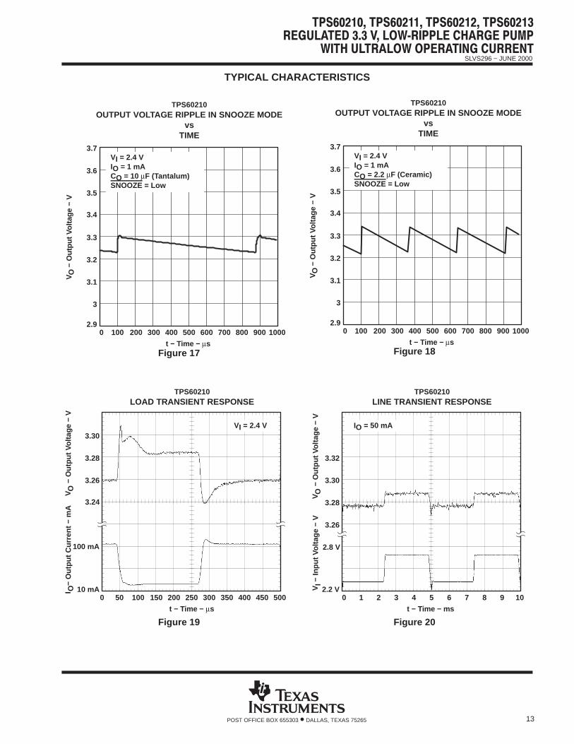
VO Output voltage ripplevs Time in snooze mode 17, 18
Load transient response 19
Line transient response 20
NOTE: All typical characteristics were measured using the typical application circuit of Figure 21 (unless otherwise noted).
Figure 3
0.1
IO − Output Current − mA
TPS60210EFFICIENCY
vsOUTPUT CURRENT
1 10 100 1000
VI = 2.4 V
VI = 1.8 V
VI = 2.7 V
Effi
cien
cy −
%
100
90
80
70
60
50
40
30
20
10
0
Figure 4
0.1
IO − Output Current − mA
TPS60212EFFICIENCY
vsOUTPUT CURRENT
Effi
cien
cy −
%
1 10 100
VI = 1.8 V
VI = 2.4 V
VI = 2.7 V
100
90
80
70
60
50
40
30
20
10
0

SLVS296 − JUNE 2000
10 POST OFFICE BOX 655303 • DALLAS, TEXAS 75265
TYPICAL CHARACTERISTICS
Figure 5
TPS60210EFFICIENCY
vsINPUT VOLTAGE
0
10
20
30
40
50
60
70
80
90
100
1.6 2.0 2.4 2.8 3.2 3.6VI − Input Voltage − V
Effi
cien
cy −
%
IO = 50 mA
Figure 6
TPS60210PEAK OUTPUT CURRENT
vsINPUT VOLTAGE
150
100
50
01.6 2.0 2.4 2.8
200
250
350
3.2 3.6
300
VI − Input Voltage − V
I −
Out
put C
urre
nt −
mA
O
Figure 7
TPS60210OUTPUT VOLTAGE
vsOUTPUT CURRENT
3.2
2.9
3.5
3.4
3.3
3.1
3.0
V O−
Out
put V
olta
ge −
V
VI = 1.8 V
VI = 2.4 V
VI = 2.7 V
VI = 3.6 V
IO − Output Current − mA
1 10 100 1000
Figure 8
3
3.05
3.10
3.15
3.20
3.25
3.30
3.35
1 10 100
VI = 3.6 VVI = 2.7 V
VI = 2.4 VVI = 1.8 V
− O
utpu
t Vol
tage
− V
TPS60212OUTPUT VOLTAGE
vsOUTPUT CURRENT
VO
IO − Output Current − mA

SLVS296 − JUNE 2000
11POST OFFICE BOX 655303 • DALLAS, TEXAS 75265
TYPICAL CHARACTERISTICS
Figure 9
TPS60210OUTPUT VOLTAGE
vs INPUT VOLTAGE
3.0
2.9
2.8
2.71.6 2.0 2.4 2.8
3.1
3.2
3.4
3.2 3.6
3.3
1 mA
50 mA100 mA
V O−
Out
put V
olta
ge −
V
VI − Input Voltage − V
Figure 10
TPS60212OUTPUT VOLTAGE
vs INPUT VOLTAGE
3.15
3.10
3.05
3.001.6 2.0 2.4 2.8
3.20
3.25
3.35
3.2 3.6
3.30
1 mA
25 mA50 mA
V O−
Out
put V
olta
ge −
V
VI − Input Voltage − V
Figure 11
30
28
24
22
20
38
26
1.6 1.8 2.0 2.2 2.4 2.6 2.8
34
32
36
V − Input Voltage − V
QUIESCENT SUPPLY CURRENTvs
INPUT VOLTAGE40
3.0 3.2 3.4 3.6
I −
Qui
esce
nt C
urre
nt −
Aµ
Q
I
IO = 0 mASNOOZE = VI
Figure 12
0
10
20
30
40
50
60
70
0 0.2 0.4 0.6 0.8 1 1.2 1.4 1.6 1.8 2
QUIESCENT SUPPLY CURRENTvs
OUTPUT CURRENT IN SNOOZE MODE
IO − Output Current − mA
I −
Qui
esce
nt C
urre
nt −
Aµ
Q
VI = 2.4 VSNOOZE = GND

SLVS296 − JUNE 2000
12 POST OFFICE BOX 655303 • DALLAS, TEXAS 75265
TYPICAL CHARACTERISTICS
Figure 13
0 50 100 150 200 250 300
SN
OO
ZE
350 400 450 500
3.3
3.2
3.5
3.6
3.4
t − Time − ms
− O
utpu
t Vol
tage
− V
VO
High
Low
TPS60210OUTPUT VOLTAGE
vsTIME
Figure 14t − Time − µs
TPS60210OUTPUT VOLTAGE RIPPLE
vsTIME
0 503.22
3.24
3.34
3.38
3.36
3.32
3.30
3.26
3.28
5 454035302510 15 20
− O
utpu
t Vol
tage
− V
VO
VI = 2.4 VIO = 1 mA
Figure 15
t − Time − µs
TPS60210OUTPUT VOLTAGE RIPPLE
vsTIME
0 103.22
3.24
3.34
3.38
3.36
3.32
3.30
3.26
3.28
1 987652 3 4
− O
utpu
t Vol
tage
− V
VO
VI = 2.4 VIO = 10 mA
Figure 16
t − Time − µs
TPS60210OUTPUT VOLTAGE RIPPLE
vsTIME
3.30
3.28
3.24
3.220 1 2 3 4 5 6
3.34
3.36
3.38
7 8 9 10
VI = 2.4 VIO = 100 mA
3.32
3.26
− O
utpu
t Vol
tage
− V
VO
SLVS296 − JUNE 2000
13POST OFFICE BOX 655303 • DALLAS, TEXAS 75265
TYPICAL CHARACTERISTICS
3.3
3.2
3.1
2.90 100 200 300 400 500 600
3.5
3.6
TPS60210OUTPUT VOLTAGE RIPPLE IN SNOOZE MODE
vsTIME
3.7
700 800 900 1000
3.4
3
t − Time − µs
− O
utpu
t Vol
tage
− V
VO
VI = 2.4 VIO = 1 mACO = 10 µF (Tantalum)SNOOZE = Low
Figure 17
3.3
3.2
3.1
2.90 100 200 300 400 500 600
3.5
3.6
TPS60210OUTPUT VOLTAGE RIPPLE IN SNOOZE MODE
vsTIME
3.7
700 800 900 1000
3.4
3
t − Time − µs
− O
utpu
t Vol
tage
− V
VO
VI = 2.4 VIO = 1 mACO = 2.2 µF (Ceramic)SNOOZE = Low
Figure 18
Figure 19
TPS60210LOAD TRANSIENT RESPONSE
100 mA
10 mA0 50 100 150 200 250 300
− O
utpu
t Vol
tage
− V
3.26
3.28
3.30
350 400 450 500
3.24
VO
− O
utpu
t Cur
rent
− m
AI O
t − Time − µs
VI = 2.4 V
Figure 20
TPS60210LINE TRANSIENT RESPONSE
3.30
3.26
2.2 V0 1 2 3 4 5 6
3.32
7 8 9 10
IO = 50 mA
3.28
2.8 V
− O
utpu
t Vol
tage
− V
VO
− In
put V
olta
ge −
VV
I
t − Time − ms

SLVS296 − JUNE 2000
14 POST OFFICE BOX 655303 • DALLAS, TEXAS 75265
APPLICATION INFORMATION
capacitor selection
The TPS6021x devices require only four external capacitors to achieve a very low output voltage ripple. Thecapacitor values are closely linked to the required output current. Low ESR (< 0.1-Ω) capacitors should be usedat the input and output of the charge pump. In general, the transfer capacitors (C1 and C2) will be the smallest.A 1-µF value is recommended if full load current performance is needed. With smaller capacitor values, themaximum possible load current is reduced and the linskip threshold is lowered.
The input capacitor improves system efficiency by reducing the input impedance. It also stabilizes the inputcurrent of the power source. The input capacitor should be chosen according to the power supply used, thedistance from the power source to the converter IC. CI is recommended to be about two to four times as largeas the flying capacitors C1 and C2.
The minimum required capacitance is 2.2 µF. Larger values will improve the load transient performance andwill reduce the maximum output ripple voltage. The larger the output capacitor, the better the output voltageaccuracy, and the more output current can be drawn from the converter when programmed into snooze mode.
Only ceramic capacitors are recommended for input, output and flying capacitors. Depending on the materialused to manufacture them, ceramic capacitors might lose their capacitance over temperature and voltage.Ceramic capacitors of type X7R or X5R material will keep their capacitance over temperature and voltage,whereas Z5U- or Y5V-type capacitors will decrease in capacitance. Table 1 lists recommended capacitorvalues.

SLVS296 − JUNE 2000
15POST OFFICE BOX 655303 • DALLAS, TEXAS 75265
APPLICATION INFORMATION
Table 2. Recommended Capacitor Values (Ceramic X5R and X7R)
LOAD CURRENT,ILOAD(mA)
FLYINGCAPACITORS,
C1/C2(µF)
INPUTCAPACITOR,
CIN(µF)
OUTPUTCAPACITOR,
COUT(µF)
OUTPUT VOLTAGERIPPLE IN LINEAR MODE,
VP-P(mV)
OUTPUT VOLTAGERIPPLE IN SKIP MODE,
VP-P(mV)
0−100 1 2.2 2.2 3 20
0−100 1 4.7 4.7 3 10
0−100 1 2.2 10 3 7
0−100 2.2 4.7 4.7 3 10
0−50 0.47 2.2 2.2 3 20
0−25 0.22 2.2 2.2 5 15
0−10 0.1 2.2 2.2 5 15
Table 3. Recommended Capacitor Types
MANUFACTURER PART NUMBER SIZE CAPACITANCE TYPE
Taiyo Yuden UMK212BJ104MG 0805 0.1 µF CeramicTaiyo Yuden
EMK212BJ224MG 0805 0.22 µF Ceramic
EMK212BJ474MG 0805 0.47 µF Ceramic
LMK212BJ105KG 0805 1 µF Ceramic
LMK212BJ225MG 0805 2.2 µF Ceramic
EMK316BJ225KL 1206 2.2 µF Ceramic
LMK316BJ475KL 1206 4.7 µF Ceramic
JMK316BJ106ML 1206 10 µF Ceramic
AVX 0805ZC105KAT2A 0805 1 µF CeramicAVX
1206ZC225KAT2A 1206 2.2 µF Ceramic
Table 4. Recommended Capacitor Manufacturers
MANUFACTURER CAPACITOR TYPE INTERNET SITE
Taiyo Yuden X7R/X5R ceramic http://www.t−yuden.com/
AVX X7R/X5R ceramic http://www.avxcorp.com/

SLVS296 − JUNE 2000
16 POST OFFICE BOX 655303 • DALLAS, TEXAS 75265
APPLICATION INFORMATION
typical operating circuit TPS60210
OUTPUT3.3 V, 100 mA
INPUT1.8 V to 3.6 V
ON/OFF
C11µF C2
1µF
Co2.2 µFCi
2.2 µFR1
R2
1
2
3
4
5
6
7
89
10
R3
Low BatteryWarning
IN
C1−
C1+
LBI
TPS60210
OUT
C2−
C2+
LBO
GNDSNOOZE
Figure 21. Typical Operating Circuit TPS60210 With Low-Battery Comparator
OUTPUT3.3 V, 50 mA
INPUT1.6 V to 3.6 V
ON/OFF
C10.47 µF C2
0.47µF
Co2.2 µFCi
2.2 µFR1
R2
1
2
3
4
5
6
7
8
9
10
R3
Low BatteryWarning
IN
C1−
C1+
LBI
TPS60212
OUT
C2−
C2+
LBO
GNDSNOOZE
Figure 22. Typical Operating Circuit TPS60212 With Low-Battery Comparator
The current losses through the resistive divider used to set the low-battery threshold can be avoided if anadditional MOSFET (like BSS138) is used in series to the resistors. This switch is controlled using the SNOOZEsignal. When the SNOOZE-signal is taken high, the device is programmed into normal operating mode, theswitch will turn on and the resistive divider draws current to set the LBI threshold voltage. When SNOOZE istaken low, the device is programmed into snooze mode during which the low-battery comparator is disabled.In addition, the resistive divider R1/R2 is disconnected from GND and therefore draws no current from thebattery. A typical schematic for this circuit is shown in Figure 22.

SLVS296 − JUNE 2000
17POST OFFICE BOX 655303 • DALLAS, TEXAS 75265
APPLICATION INFORMATION
typical operating circuit TPS60211
OUTPUT3.3 V, 100 mA
INPUT1.8 V to 3.6 V
ON/OFF
C11 µF C2
1 µF
Co2.2 µFCi
2.2 µF
3
4
5
6
7
89
10
R1
Power-Good Signal
IN
C1−
C1+
TPS60211
OUT
C2−
C2+
PG
GND1,2
SNOOZE
Figure 23. Typical Operating Circuit TPS60211 With Power-Good Comparator
power dissipation
The power dissipated in the TPS6021x devices depends mainly on input voltage (VI) and output current (IO)and is approximated by:
P(DISS) IO x 2 x VI VO for I(Q) IO (5)
By observing equation 5, it can be seen that the power dissipation is worse with a higher input voltage and ahigher output current. For an input voltage of 3.6 V and an output current of 100 mA, the calculated powerdissipation (P(DISS)) is 390 mW. This is also the point where the charge pump operates with its lowest efficiency.
With the recommended maximum junction temperature of 125°C and an assumed maximum ambient operatingtemperature of 85°C, the maximum allowed thermal resistance junction to ambient of the system can becalculated.
RJA(max)
TJ(MAX) TAPDISS(max)
125°C 85°C390 mW
102°CW (6)
PDISS must be less than that allowed by the package rating. The thermal resistance junction to ambient of theused 10-pin MSOP is 294°C/W for an unsoldered package. The thermal resistance junction to ambient with theIC soldered to a printed circuit using a board layout as described in the application information section, the RΘJAis typically 200°C/W, which is higher than the maximum value calculated previously. However, in a batterypowered application, both the VI and the ambient temperature (TA) will typically be lower than the worst caseratings used in equation 6, and PDISS should not be a problem in most applications.
layout and board space
Careful board layout is necessary due to the high transient currents and switching frequency of the converter.All capacitors should be placed in close proximity to the device. A PCB layout proposal for a one-layer boardis given in Figure 24.
An evaluation module for the TPS60210 is available and can be ordered under product codeTPS60210EVM−167. The EVM uses the layout shown in Figure 26. The EVM has the form factor of a 14-pindual in-line package and can be mounted accordingly on a socket. All components, including the pins, areshown in Figure 24. The actual size of the EVM is 17,9 mm x 10,2 mm = 182,6 mm2.

SLVS296 − JUNE 2000
18 POST OFFICE BOX 655303 • DALLAS, TEXAS 75265
APPLICATION INFORMATION
layout and board space (continued)
Figure 24. Recommended Component Placement and Board Layout
17,9 mm
10,2 mm
C1
C2
C3
C4
R2
C5
R3
R4R
1IC1
Table 5. Component Identification
IC1 TPS60210
C1, C2 Flying capacitors
C3 Input capacitor
C4 Output capacitor
C5 Stabilization capacitor for LBI
R1, R2 Resistive divider for LBI
R3 Pullup resistor for LBO
R4 Pullup resistor for EN
Capacitor C5 should be included if large line transients are expected. This capacitor suppresses toggling of theLBO due to these line changes.

SLVS296 − JUNE 2000
19POST OFFICE BOX 655303 • DALLAS, TEXAS 75265
APPLICATION INFORMATION
device family products
Other charge pump dc-dc converters from Texas Instruments are:
Table 6. Product Identification
PART NUMBER LITERATURENUMBER
DESCRIPTION
TPS60100 SLVS213 2-cell to regulated 3.3-V, 200-mA low-noise charge pump
TPS60101 SLVS214 2-cell to regulated 3.3-V, 100-mA low-noise charge pump
TPS60110 SLVS215 3-cell to regulated 5.0-V, 300-mA low-noise charge pump
TPS60111 SLVS216 3-cell to regulated 5.0-V, 150-mA low-noise charge pump
TPS60120 SLVS257 2-cell to regulated 3.3-V, 200-mA high-efficiency charge pump with low-battery comparator
TPS60121 SLVS257 2-cell to regulated 3.3-V, 200-mA high-efficiency charge pump with power-good comparator
TPS60122 SLVS257 2-cell to regulated 3.3-V, 100-mA high-efficiency charge pump with low-battery comparator
TPS60123 SLVS257 2-cell to regulated 3.3-V, 100-mA high-efficiency charge pump with power-good comparator
TPS60130 SLVS258 3-cell to regulated 5.0-V, 300-mA high-efficiency charge pump with low-battery comparator
TPS60131 SLVS258 3-cell to regulated 5.0-V, 300-mA high-efficiency charge pump with power-good comparator
TPS60132 SLVS258 3-cell to regulated 5.0-V, 150-mA high-efficiency charge pump with low-battery comparator
TPS60133 SLVS258 3-cell to regulated 5.0-V, 150-mA high-efficiency charge pump with power-good comparator
TPS60140 SLVS273 2-cell to regulated 5.0-V, 100-mA charge pump voltage tripler with low-battery comparator
TPS60141 SLVS273 2-cell to regulated 5.0-V, 100-mA charge pump voltage tripler with power-good comparator
TPS60200 SLVS274 2-cell to regulated 3.3-V, 100-mA low-ripple charge pump with low-battery comparator
TPS60201 SLVS274 2-cell to regulated 3.3-V, 100-mA low-ripple charge pump with power-good comparator
TPS60202 SLVS274 2-cell to regulated 3.3-V, 50-mA low-ripple charge pump with low-battery comparator
TPS60203 SLVS274 2-cell to regulated 3.3-V, 50-mA low-ripple charge pump with power-good comparator

PACKAGE OPTION ADDENDUM
www.ti.com 9-Sep-2014
Addendum-Page 1
PACKAGING INFORMATION
Orderable Device Status(1)
Package Type PackageDrawing
Pins PackageQty
Eco Plan(2)
Lead/Ball Finish(6)
MSL Peak Temp(3)
Op Temp (°C) Device Marking(4/5)
Samples
TPS60210DGS ACTIVE VSSOP DGS 10 80 Green (RoHS& no Sb/Br)
CU NIPDAU |CU NIPDAUAG
Level-1-260C-UNLIM -40 to 85 AFD
TPS60210DGSG4 ACTIVE VSSOP DGS 10 80 Green (RoHS& no Sb/Br)
CU NIPDAU Level-1-260C-UNLIM -40 to 85 AFD
TPS60210DGSR ACTIVE VSSOP DGS 10 2500 Green (RoHS& no Sb/Br)
CU NIPDAU |CU NIPDAUAG
Level-1-260C-UNLIM -40 to 85 AFD
TPS60210DGSRG4 ACTIVE VSSOP DGS 10 2500 Green (RoHS& no Sb/Br)
CU NIPDAU Level-1-260C-UNLIM -40 to 85 AFD
TPS60211DGS ACTIVE VSSOP DGS 10 80 Green (RoHS& no Sb/Br)
CU NIPDAU Level-1-260C-UNLIM -40 to 85 AFE
TPS60211DGSG4 ACTIVE VSSOP DGS 10 80 Green (RoHS& no Sb/Br)
CU NIPDAU Level-1-260C-UNLIM -40 to 85 AFE
TPS60212DGS ACTIVE VSSOP DGS 10 80 Green (RoHS& no Sb/Br)
CU NIPDAU Level-1-260C-UNLIM -40 to 85 AFF
TPS60212DGSG4 ACTIVE VSSOP DGS 10 80 Green (RoHS& no Sb/Br)
CU NIPDAU Level-1-260C-UNLIM -40 to 85 AFF
TPS60212DGSR ACTIVE VSSOP DGS 10 2500 Green (RoHS& no Sb/Br)
CU NIPDAU Level-1-260C-UNLIM -40 to 85 AFF
TPS60212DGSRG4 ACTIVE VSSOP DGS 10 2500 Green (RoHS& no Sb/Br)
CU NIPDAU Level-1-260C-UNLIM -40 to 85 AFF
TPS60213DGS ACTIVE VSSOP DGS 10 80 Green (RoHS& no Sb/Br)
CU NIPDAU Level-1-260C-UNLIM -40 to 85 AFG
TPS60213DGSG4 ACTIVE VSSOP DGS 10 80 Green (RoHS& no Sb/Br)
CU NIPDAU Level-1-260C-UNLIM -40 to 85 AFG
TPS60213DGSR ACTIVE VSSOP DGS 10 2500 Green (RoHS& no Sb/Br)
CU NIPDAU Level-1-260C-UNLIM -40 to 85 AFG
(1) The marketing status values are defined as follows:ACTIVE: Product device recommended for new designs.LIFEBUY: TI has announced that the device will be discontinued, and a lifetime-buy period is in effect.NRND: Not recommended for new designs. Device is in production to support existing customers, but TI does not recommend using this part in a new design.PREVIEW: Device has been announced but is not in production. Samples may or may not be available.OBSOLETE: TI has discontinued the production of the device.

PACKAGE OPTION ADDENDUM
www.ti.com 9-Sep-2014
Addendum-Page 2
(2) Eco Plan - The planned eco-friendly classification: Pb-Free (RoHS), Pb-Free (RoHS Exempt), or Green (RoHS & no Sb/Br) - please check http://www.ti.com/productcontent for the latest availabilityinformation and additional product content details.TBD: The Pb-Free/Green conversion plan has not been defined.Pb-Free (RoHS): TI's terms "Lead-Free" or "Pb-Free" mean semiconductor products that are compatible with the current RoHS requirements for all 6 substances, including the requirement thatlead not exceed 0.1% by weight in homogeneous materials. Where designed to be soldered at high temperatures, TI Pb-Free products are suitable for use in specified lead-free processes.Pb-Free (RoHS Exempt): This component has a RoHS exemption for either 1) lead-based flip-chip solder bumps used between the die and package, or 2) lead-based die adhesive used betweenthe die and leadframe. The component is otherwise considered Pb-Free (RoHS compatible) as defined above.Green (RoHS & no Sb/Br): TI defines "Green" to mean Pb-Free (RoHS compatible), and free of Bromine (Br) and Antimony (Sb) based flame retardants (Br or Sb do not exceed 0.1% by weightin homogeneous material)
(3) MSL, Peak Temp. - The Moisture Sensitivity Level rating according to the JEDEC industry standard classifications, and peak solder temperature.
(4) There may be additional marking, which relates to the logo, the lot trace code information, or the environmental category on the device.
(5) Multiple Device Markings will be inside parentheses. Only one Device Marking contained in parentheses and separated by a "~" will appear on a device. If a line is indented then it is a continuationof the previous line and the two combined represent the entire Device Marking for that device.
(6) Lead/Ball Finish - Orderable Devices may have multiple material finish options. Finish options are separated by a vertical ruled line. Lead/Ball Finish values may wrap to two lines if the finishvalue exceeds the maximum column width.
Important Information and Disclaimer:The information provided on this page represents TI's knowledge and belief as of the date that it is provided. TI bases its knowledge and belief on informationprovided by third parties, and makes no representation or warranty as to the accuracy of such information. Efforts are underway to better integrate information from third parties. TI has taken andcontinues to take reasonable steps to provide representative and accurate information but may not have conducted destructive testing or chemical analysis on incoming materials and chemicals.TI and TI suppliers consider certain information to be proprietary, and thus CAS numbers and other limited information may not be available for release.
In no event shall TI's liability arising out of such information exceed the total purchase price of the TI part(s) at issue in this document sold by TI to Customer on an annual basis.

TAPE AND REEL INFORMATION
*All dimensions are nominal
Device PackageType
PackageDrawing
Pins SPQ ReelDiameter
(mm)
ReelWidth
W1 (mm)
A0(mm)
B0(mm)
K0(mm)
P1(mm)
W(mm)
Pin1Quadrant
TPS60210DGSR VSSOP DGS 10 2500 330.0 12.4 5.3 3.4 1.4 8.0 12.0 Q1
TPS60212DGSR VSSOP DGS 10 2500 330.0 12.4 5.3 3.4 1.4 8.0 12.0 Q1
TPS60213DGSR VSSOP DGS 10 2500 330.0 12.4 5.3 3.4 1.4 8.0 12.0 Q1
PACKAGE MATERIALS INFORMATION
www.ti.com 19-Nov-2012
Pack Materials-Page 1

*All dimensions are nominal
Device Package Type Package Drawing Pins SPQ Length (mm) Width (mm) Height (mm)
TPS60210DGSR VSSOP DGS 10 2500 340.5 338.1 20.6
TPS60212DGSR VSSOP DGS 10 2500 340.5 338.1 20.6
TPS60213DGSR VSSOP DGS 10 2500 340.5 338.1 20.6
PACKAGE MATERIALS INFORMATION
www.ti.com 19-Nov-2012
Pack Materials-Page 2


IMPORTANT NOTICETexas Instruments Incorporated and its subsidiaries (TI) reserve the right to make corrections, enhancements, improvements and otherchanges to its semiconductor products and services per JESD46, latest issue, and to discontinue any product or service per JESD48, latestissue. Buyers should obtain the latest relevant information before placing orders and should verify that such information is current andcomplete. All semiconductor products (also referred to herein as “components”) are sold subject to TI’s terms and conditions of salesupplied at the time of order acknowledgment.TI warrants performance of its components to the specifications applicable at the time of sale, in accordance with the warranty in TI’s termsand conditions of sale of semiconductor products. Testing and other quality control techniques are used to the extent TI deems necessaryto support this warranty. Except where mandated by applicable law, testing of all parameters of each component is not necessarilyperformed.TI assumes no liability for applications assistance or the design of Buyers’ products. Buyers are responsible for their products andapplications using TI components. To minimize the risks associated with Buyers’ products and applications, Buyers should provideadequate design and operating safeguards.TI does not warrant or represent that any license, either express or implied, is granted under any patent right, copyright, mask work right, orother intellectual property right relating to any combination, machine, or process in which TI components or services are used. Informationpublished by TI regarding third-party products or services does not constitute a license to use such products or services or a warranty orendorsement thereof. Use of such information may require a license from a third party under the patents or other intellectual property of thethird party, or a license from TI under the patents or other intellectual property of TI.Reproduction of significant portions of TI information in TI data books or data sheets is permissible only if reproduction is without alterationand is accompanied by all associated warranties, conditions, limitations, and notices. TI is not responsible or liable for such altereddocumentation. Information of third parties may be subject to additional restrictions.Resale of TI components or services with statements different from or beyond the parameters stated by TI for that component or servicevoids all express and any implied warranties for the associated TI component or service and is an unfair and deceptive business practice.TI is not responsible or liable for any such statements.Buyer acknowledges and agrees that it is solely responsible for compliance with all legal, regulatory and safety-related requirementsconcerning its products, and any use of TI components in its applications, notwithstanding any applications-related information or supportthat may be provided by TI. Buyer represents and agrees that it has all the necessary expertise to create and implement safeguards whichanticipate dangerous consequences of failures, monitor failures and their consequences, lessen the likelihood of failures that might causeharm and take appropriate remedial actions. Buyer will fully indemnify TI and its representatives against any damages arising out of the useof any TI components in safety-critical applications.In some cases, TI components may be promoted specifically to facilitate safety-related applications. With such components, TI’s goal is tohelp enable customers to design and create their own end-product solutions that meet applicable functional safety standards andrequirements. Nonetheless, such components are subject to these terms.No TI components are authorized for use in FDA Class III (or similar life-critical medical equipment) unless authorized officers of the partieshave executed a special agreement specifically governing such use.Only those TI components which TI has specifically designated as military grade or “enhanced plastic” are designed and intended for use inmilitary/aerospace applications or environments. Buyer acknowledges and agrees that any military or aerospace use of TI componentswhich have not been so designated is solely at the Buyer's risk, and that Buyer is solely responsible for compliance with all legal andregulatory requirements in connection with such use.TI has specifically designated certain components as meeting ISO/TS16949 requirements, mainly for automotive use. In any case of use ofnon-designated products, TI will not be responsible for any failure to meet ISO/TS16949.Products ApplicationsAudio www.ti.com/audio Automotive and Transportation www.ti.com/automotiveAmplifiers amplifier.ti.com Communications and Telecom www.ti.com/communicationsData Converters dataconverter.ti.com Computers and Peripherals www.ti.com/computersDLP® Products www.dlp.com Consumer Electronics www.ti.com/consumer-appsDSP dsp.ti.com Energy and Lighting www.ti.com/energyClocks and Timers www.ti.com/clocks Industrial www.ti.com/industrialInterface interface.ti.com Medical www.ti.com/medicalLogic logic.ti.com Security www.ti.com/securityPower Mgmt power.ti.com Space, Avionics and Defense www.ti.com/space-avionics-defenseMicrocontrollers microcontroller.ti.com Video and Imaging www.ti.com/videoRFID www.ti-rfid.comOMAP Applications Processors www.ti.com/omap TI E2E Community e2e.ti.comWireless Connectivity www.ti.com/wirelessconnectivity
Mailing Address: Texas Instruments, Post Office Box 655303, Dallas, Texas 75265Copyright © 2014, Texas Instruments Incorporated