Embed Size (px)
Citation preview
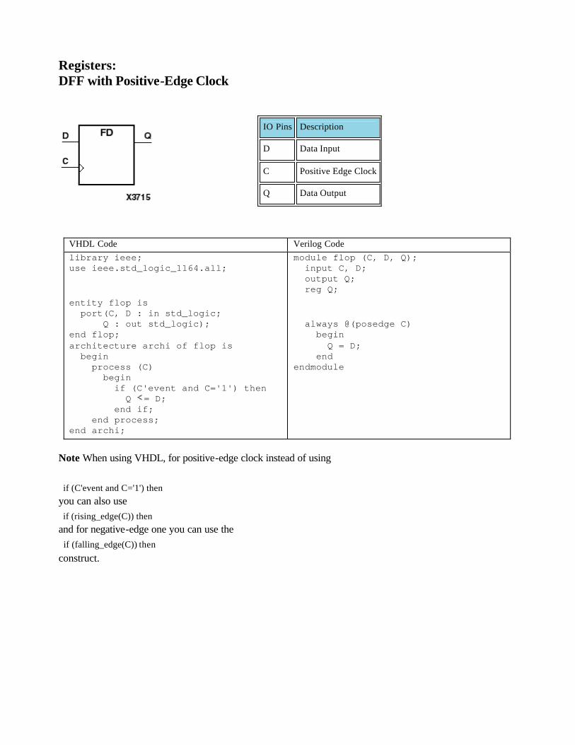
Registers: DFF with Positive-Edge Clock
IO Pins Description
D Data Input
C Positive Edge Clock
Q Data Output
VHDL Code Verilog Code library ieee; use ieee.std_logic_1164.all; entity flop is port(C, D : in std_logic; Q : out std_logic); end flop; architecture archi of flop is begin process (C) begin if (C'event and C='1') then Q = D; end if; end process; end archi;
module flop (C, D, Q); input C, D; output Q; reg Q; always @(posedge C) begin Q = D; end endmodule
Note When using VHDL, for positive-edge clock instead of using if (C'event and C='1') then you can also use if (rising_edge(C)) then and for negative-edge one you can use the if (falling_edge(C)) then construct.
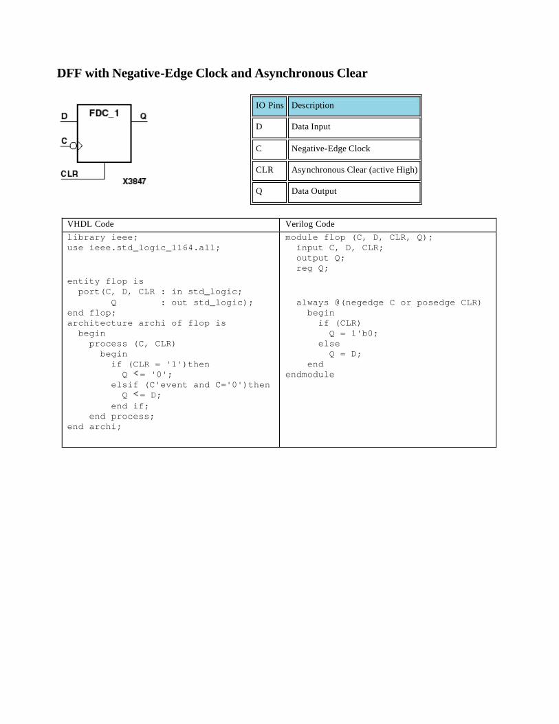
DFF with Negative-Edge Clock and Asynchronous Clear
IO Pins Description
D Data Input
C Negative-Edge Clock
CLR Asynchronous Clear (active High)
Q Data Output
VHDL Code Verilog Code library ieee; use ieee.std_logic_1164.all; entity flop is port(C, D, CLR : in std_logic; Q : out std_logic); end flop; architecture archi of flop is begin process (C, CLR) begin if (CLR = '1')then Q = '0'; elsif (C'event and C='0')then Q = D; end if; end process; end archi;
module flop (C, D, CLR, Q); input C, D, CLR; output Q; reg Q; always @(negedge C or posedge CLR) begin if (CLR) Q = 1'b0; else Q = D; end endmodule
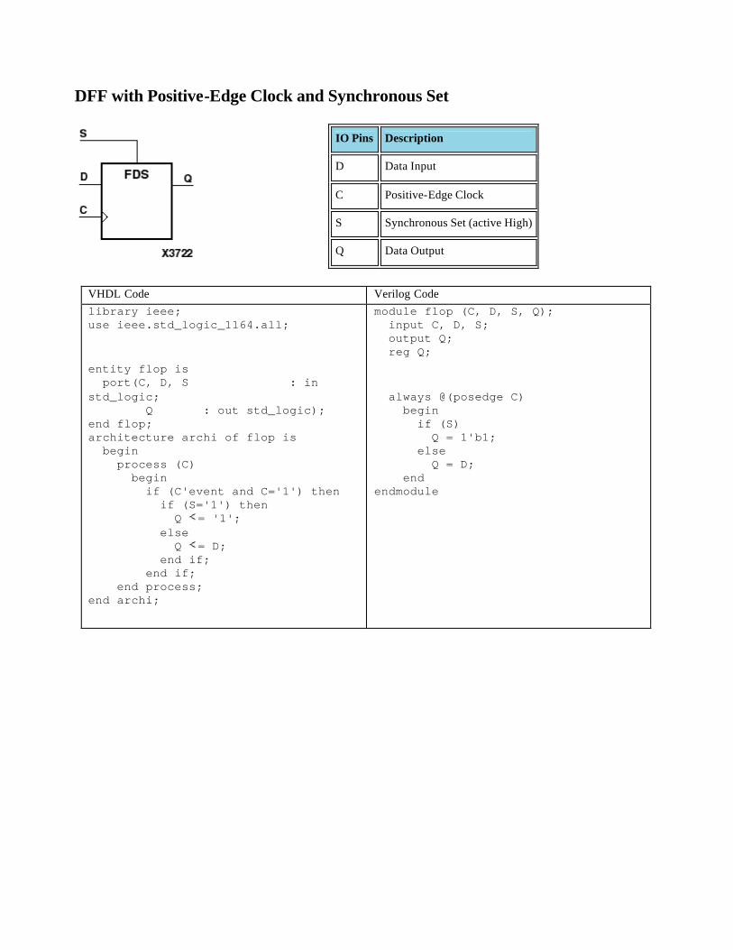
DFF with Positive-Edge Clock and Synchronous Set
IO Pins Description
D Data Input
C Positive-Edge Clock
S Synchronous Set (active High)
Q Data Output
VHDL Code Verilog Code library ieee; use ieee.std_logic_1164.all; entity flop is port(C, D, S : in std_logic; Q : out std_logic); end flop; architecture archi of flop is begin process (C) begin if (C'event and C='1') then if (S='1') then Q = '1'; else Q = D; end if; end if; end process; end archi;
module flop (C, D, S, Q); input C, D, S; output Q; reg Q; always @(posedge C) begin if (S) Q = 1'b1; else Q = D; end endmodule
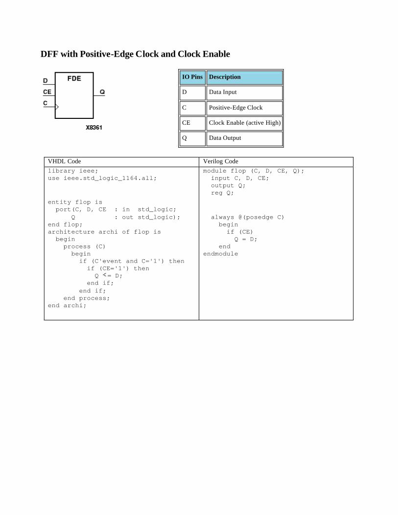
DFF with Positive-Edge Clock and Clock Enable
IO Pins Description
D Data Input
C Positive-Edge Clock
CE Clock Enable (active High)
Q Data Output
VHDL Code Verilog Code library ieee; use ieee.std_logic_1164.all; entity flop is port(C, D, CE : in std_logic; Q : out std_logic); end flop; architecture archi of flop is begin process (C) begin if (C'event and C='1') then if (CE='1') then Q = D; end if; end if; end process; end archi;
module flop (C, D, CE, Q); input C, D, CE; output Q; reg Q; always @(posedge C) begin if (CE) Q = D; end endmodule
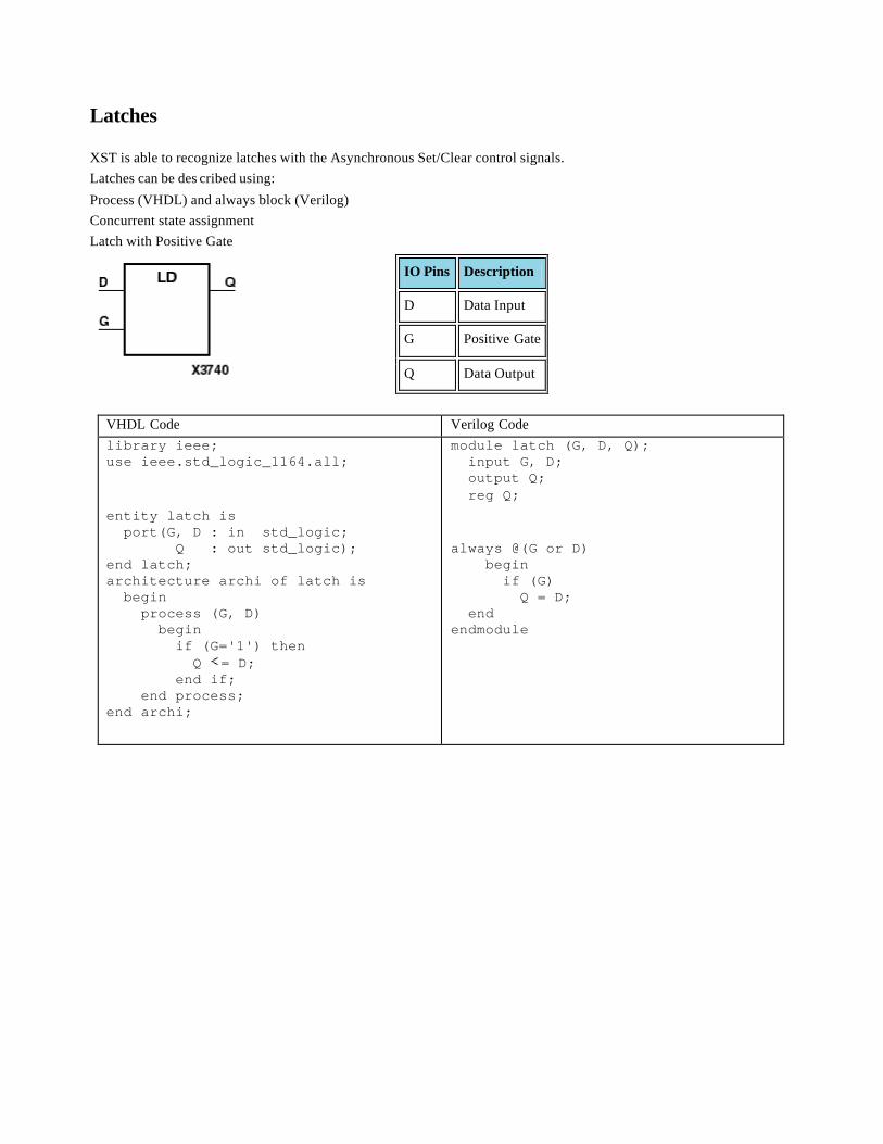
Latches
XST is able to recognize latches with the Asynchronous Set/Clear control signals. Latches can be des cribed using:
Process (VHDL) and always block (Verilog) Concurrent state assignment Latch with Positive Gate
IO Pins Description
D Data Input
G Positive Gate
Q Data Output
VHDL Code Verilog Code library ieee; use ieee.std_logic_1164.all; entity latch is port(G, D : in std_logic; Q : out std_logic); end latch; architecture archi of latch is begin process (G, D) begin if (G='1') then Q = D; end if; end process; end archi;
module latch (G, D, Q); input G, D; output Q; reg Q; always @(G or D) begin if (G) Q = D; end endmodule
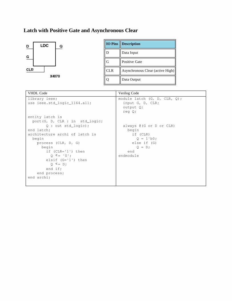
Latch with Positive Gate and Asynchronous Clear
IO Pins Description
D Data Input
G Positive Gate
CLR Asynchronous Clear (active High)
Q Data Output
VHDL Code Verilog Code library ieee; use ieee.std_logic_1164.all; entity latch is port(G, D, CLR : in std_logic; Q : out std_logic); end latch; architecture archi of latch is begin process (CLR, D, G) begin if (CLR='1') then Q = '0'; elsif (G='1') then Q = D; end if; end process; end archi;
module latch (G, D, CLR, Q); input G, D, CLR; output Q; reg Q; always @(G or D or CLR) begin if (CLR) Q = 1'b0; else if (G) Q = D; end endmodule
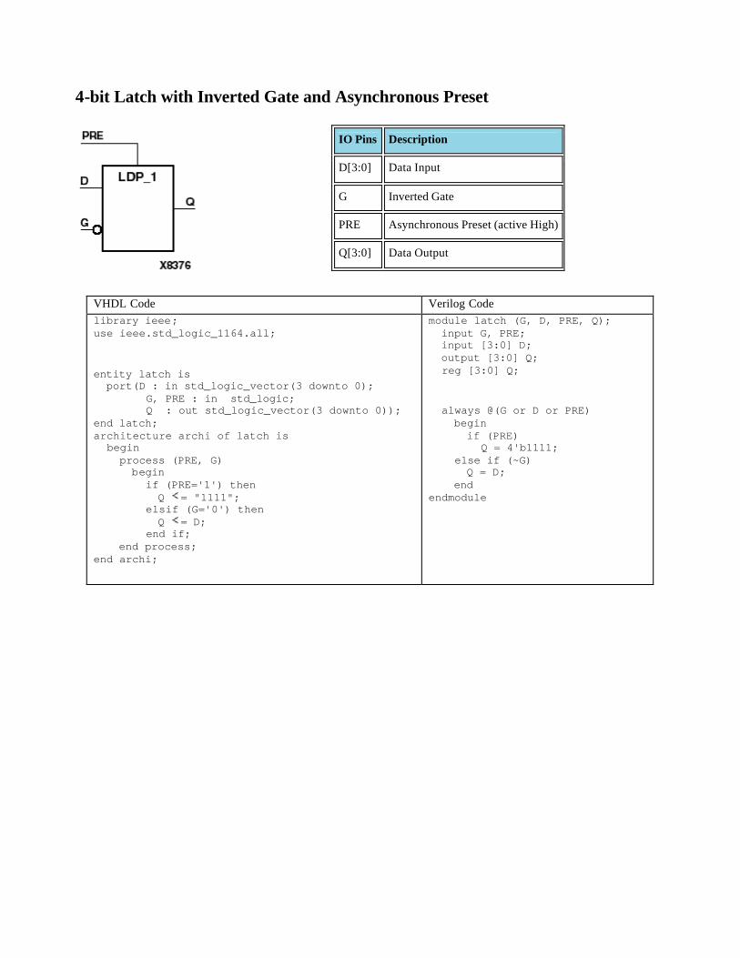
4-bit Latch with Inverted Gate and Asynchronous Preset
IO Pins Description
D[3:0] Data Input
G Inverted Gate
PRE Asynchronous Preset (active High)
Q[3:0] Data Output
VHDL Code Verilog Code library ieee; use ieee.std_logic_1164.all; entity latch is port(D : in std_logic_vector(3 downto 0); G, PRE : in std_logic; Q : out std_logic_vector(3 downto 0)); end latch; architecture archi of latch is begin process (PRE, G) begin if (PRE='1') then Q = "1111"; elsif (G='0') then Q = D; end if; end process; end archi;
module latch (G, D, PRE, Q); input G, PRE; input [3:0] D; output [3:0] Q; reg [3:0] Q; always @(G or D or PRE) begin if (PRE) Q = 4'b1111; else if (~G) Q = D; end endmodule
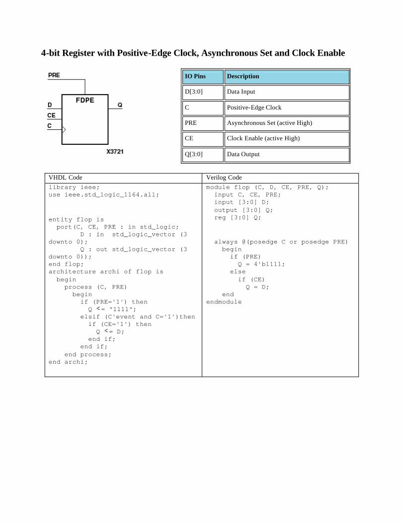
4-bit Register with Positive-Edge Clock, Asynchronous Set and Clock Enable
IO Pins Description
D[3:0] Data Input
C Positive-Edge Clock
PRE Asynchronous Set (active High)
CE Clock Enable (active High)
Q[3:0] Data Output
VHDL Code Verilog Code library ieee; use ieee.std_logic_1164.all; entity flop is port(C, CE, PRE : in std_logic; D : in std_logic_vector (3 downto 0); Q : out std_logic_vector (3 downto 0)); end flop; architecture archi of flop is begin process (C, PRE) begin if (PRE='1') then Q = "1111"; elsif (C'event and C='1')then if (CE='1') then Q = D; end if; end if; end process; end archi;
module flop (C, D, CE, PRE, Q); input C, CE, PRE; input [3:0] D; output [3:0] Q; reg [3:0] Q; always @(posedge C or posedge PRE) begin if (PRE) Q = 4'b1111; else if (CE) Q = D; end endmodule
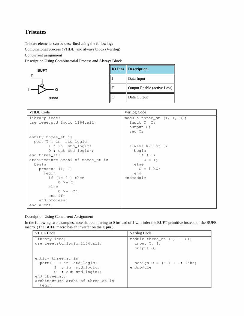
Tristates
Tristate elements can be described using the following: Combinatorial process (VHDL) and always block (Verilog)
Concurrent assignment Description Using Combinatorial Process and Always Block
IO Pins Description
I Data Input
T Output Enable (active Low)
O Data Output
VHDL Code Verilog Code library ieee; use ieee.std_logic_1164.all; entity three_st is port(T : in std_logic; I : in std_logic; O : out std_logic); end three_st; architecture archi of three_st is begin process (I, T) begin if (T='0') then O = I; else O = 'Z'; end if; end process; end archi;
module three_st (T, I, O); input T, I; output O; reg O; always @(T or I) begin if (~T) O = I; else O = 1'bZ; end endmodule
Description Using Concurrent Assignment
In the following two examples, note that comparing to 0 instead of 1 will infer the BUFT primitive instead of the BUFE macro. (The BUFE macro has an inverter on the E pin.)
VHDL Code Verilog Code library ieee; use ieee.std_logic_1164.all; entity three_st is port(T : in std_logic; I : in std_logic; O : out std_logic); end three_st; architecture archi of three_st is begin
module three_st (T, I, O); input T, I; output O; assign O = (~T) ? I: 1'bZ; endmodule
O = I when (T='0') else 'Z'; end archi;
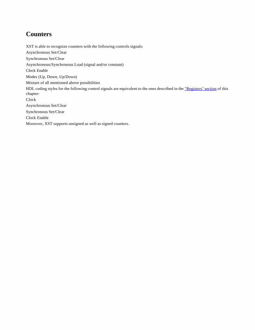
Counters
XST is able to recognize counters with the following controls signals: Asynchronous Set/Clear
Synchronous Set/Clear Asynchronous/Synchronous Load (signal and/or constant) Clock Enable
Modes (Up, Down, Up/Down) Mixture of all mentioned above possibilities HDL coding styles for the following control signals are equivalent to the ones described in the "Registers" section of this chapter: Clock Asynchronous Set/Clear
Synchronous Set/Clear Clock Enable Moreover, XST supports unsigned as well as signed counters.
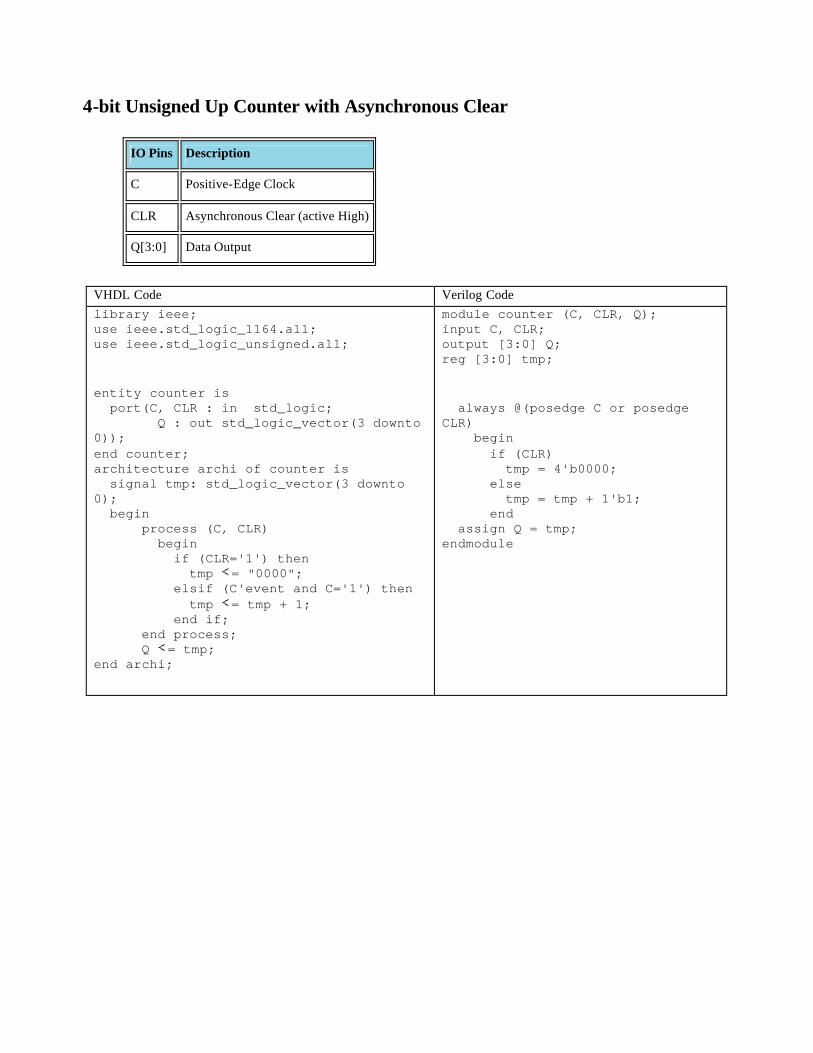
4-bit Unsigned Up Counter with Asynchronous Clear
IO Pins Description
C Positive-Edge Clock
CLR Asynchronous Clear (active High)
Q[3:0] Data Output
VHDL Code Verilog Code library ieee; use ieee.std_logic_1164.all; use ieee.std_logic_unsigned.all; entity counter is port(C, CLR : in std_logic; Q : out std_logic_vector(3 downto 0)); end counter; architecture archi of counter is signal tmp: std_logic_vector(3 downto 0); begin process (C, CLR) begin if (CLR='1') then tmp = "0000"; elsif (C'event and C='1') then tmp = tmp + 1; end if; end process; Q = tmp; end archi;
module counter (C, CLR, Q); input C, CLR; output [3:0] Q; reg [3:0] tmp; always @(posedge C or posedge CLR) begin if (CLR) tmp = 4'b0000; else tmp = tmp + 1'b1; end assign Q = tmp; endmodule
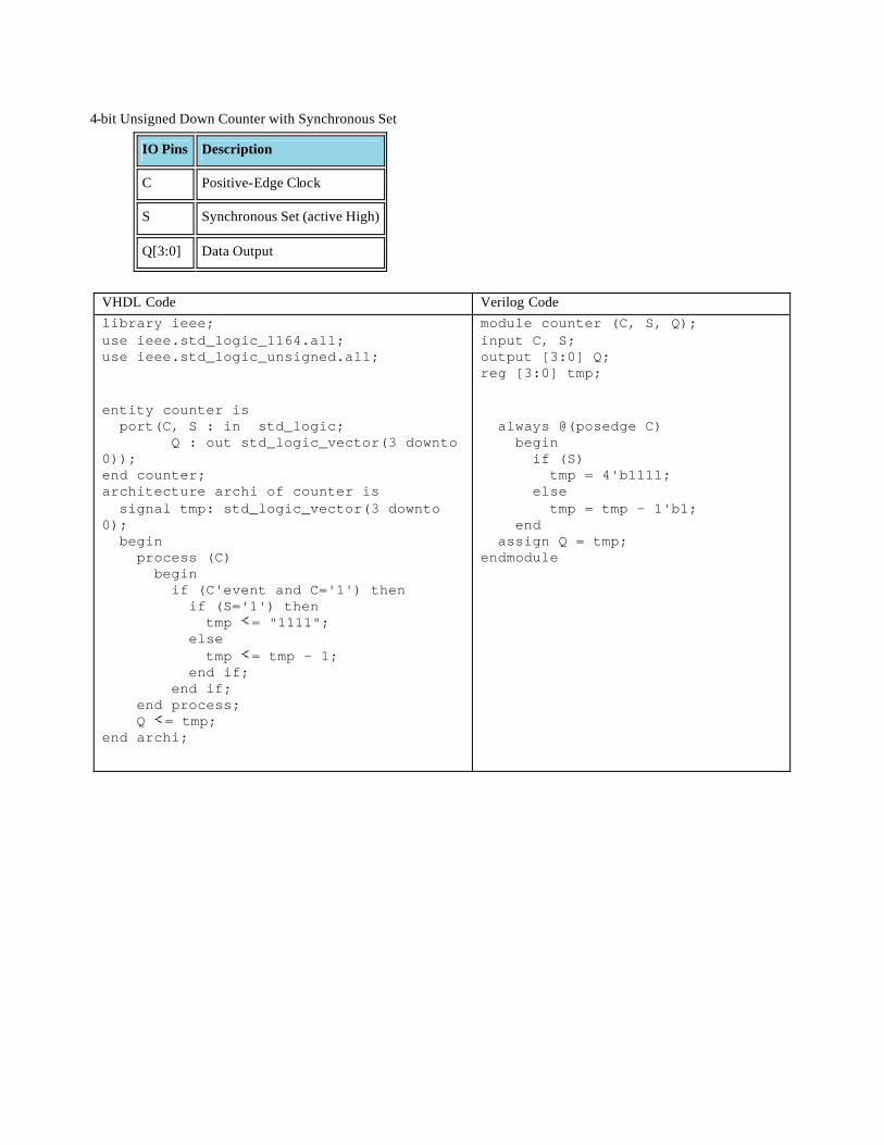
4-bit Unsigned Down Counter with Synchronous Set
IO Pins Description
C Positive-Edge Clock
S Synchronous Set (active High)
Q[3:0] Data Output
VHDL Code Verilog Code library ieee; use ieee.std_logic_1164.all; use ieee.std_logic_unsigned.all; entity counter is port(C, S : in std_logic; Q : out std_logic_vector(3 downto 0)); end counter; architecture archi of counter is signal tmp: std_logic_vector(3 downto 0); begin process (C) begin if (C'event and C='1') then if (S='1') then tmp = "1111"; else tmp = tmp - 1; end if; end if; end process; Q = tmp; end archi;
module counter (C, S, Q); input C, S; output [3:0] Q; reg [3:0] tmp; always @(posedge C) begin if (S) tmp = 4'b1111; else tmp = tmp - 1'b1; end assign Q = tmp; endmodule
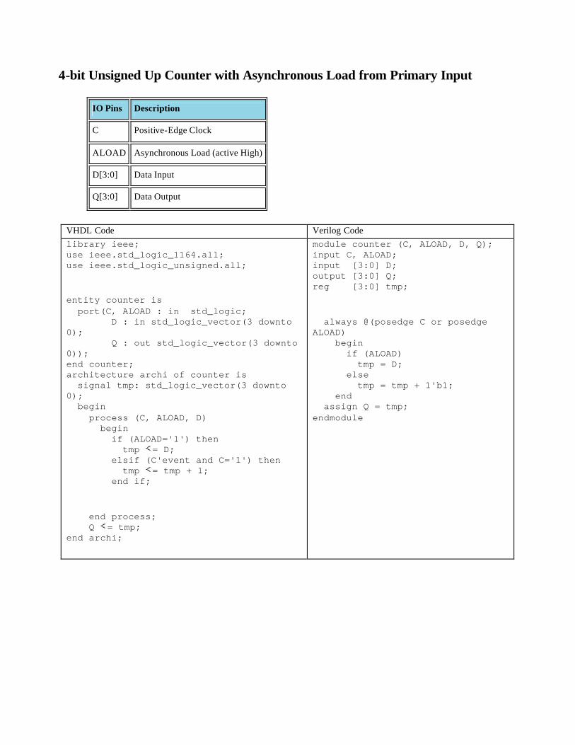
4-bit Unsigned Up Counter with Asynchronous Load from Primary Input
IO Pins Description
C Positive-Edge Clock
ALOAD Asynchronous Load (active High)
D[3:0] Data Input
Q[3:0] Data Output
VHDL Code Verilog Code library ieee; use ieee.std_logic_1164.all; use ieee.std_logic_unsigned.all; entity counter is port(C, ALOAD : in std_logic; D : in std_logic_vector(3 downto 0); Q : out std_logic_vector(3 downto 0)); end counter; architecture archi of counter is signal tmp: std_logic_vector(3 downto 0); begin process (C, ALOAD, D) begin if (ALOAD='1') then tmp = D; elsif (C'event and C='1') then tmp = tmp + 1; end if; end process; Q = tmp; end archi;
module counter (C, ALOAD, D, Q); input C, ALOAD; input [3:0] D; output [3:0] Q; reg [3:0] tmp; always @(posedge C or posedge ALOAD) begin if (ALOAD) tmp = D; else tmp = tmp + 1'b1; end assign Q = tmp; endmodule
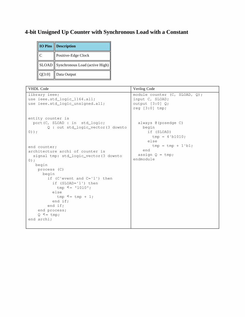
4-bit Unsigned Up Counter with Synchronous Load with a Constant
IO Pins Description
C Positive-Edge Clock
SLOAD Synchronous Load (active High)
Q[3:0] Data Output
VHDL Code Verilog Code library ieee; use ieee.std_logic_1164.all; use ieee.std_logic_unsigned.all; entity counter is port(C, SLOAD : in std_logic; Q : out std_logic_vector(3 downto 0)); end counter; architecture archi of counter is signal tmp: std_logic_vector(3 downto 0); begin process (C) begin if (C'event and C='1') then if (SLOAD='1') then tmp = "1010"; else tmp = tmp + 1; end if; end if; end process; Q = tmp; end archi;
module counter (C, SLOAD, Q); input C, SLOAD; output [3:0] Q; reg [3:0] tmp; always @(posedge C) begin if (SLOAD) tmp = 4'b1010; else tmp = tmp + 1'b1; end assign Q = tmp; endmodule
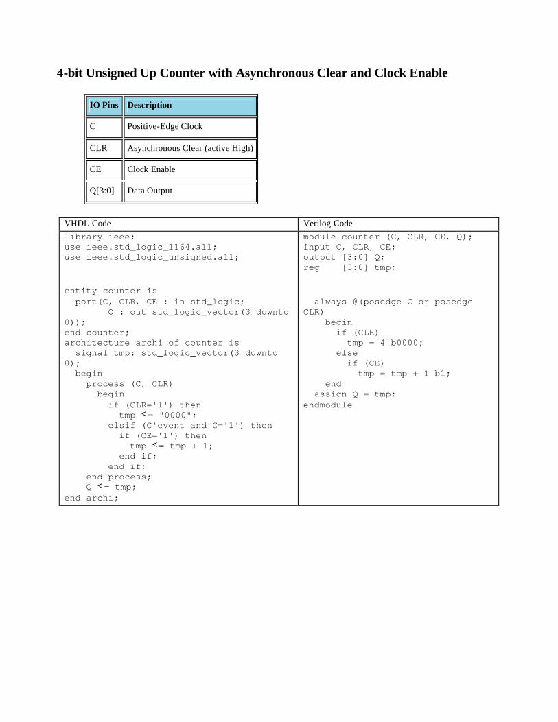
4-bit Unsigned Up Counter with Asynchronous Clear and Clock Enable
IO Pins Description
C Positive-Edge Clock
CLR Asynchronous Clear (active High)
CE Clock Enable
Q[3:0] Data Output
VHDL Code Verilog Code library ieee; use ieee.std_logic_1164.all; use ieee.std_logic_unsigned.all; entity counter is port(C, CLR, CE : in std_logic; Q : out std_logic_vector(3 downto 0)); end counter; architecture archi of counter is signal tmp: std_logic_vector(3 downto 0); begin process (C, CLR) begin if (CLR='1') then tmp = "0000"; elsif (C'event and C='1') then if (CE='1') then tmp = tmp + 1; end if; end if; end process; Q = tmp; end archi;
module counter (C, CLR, CE, Q); input C, CLR, CE; output [3:0] Q; reg [3:0] tmp; always @(posedge C or posedge CLR) begin if (CLR) tmp = 4'b0000; else if (CE) tmp = tmp + 1'b1; end assign Q = tmp; endmodule
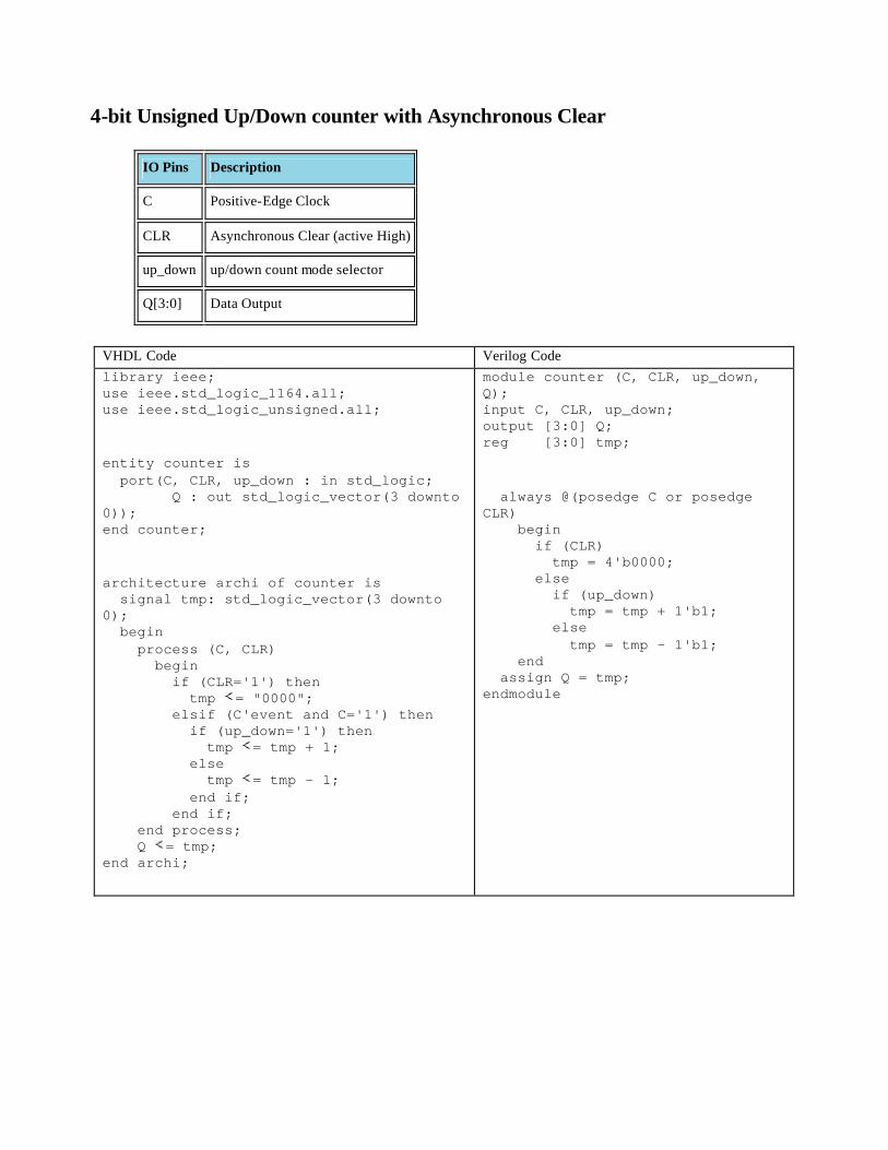
4-bit Unsigned Up/Down counter with Asynchronous Clear
IO Pins Description
C Positive-Edge Clock
CLR Asynchronous Clear (active High)
up_down up/down count mode selector
Q[3:0] Data Output
VHDL Code Verilog Code library ieee; use ieee.std_logic_1164.all; use ieee.std_logic_unsigned.all; entity counter is port(C, CLR, up_down : in std_logic; Q : out std_logic_vector(3 downto 0)); end counter; architecture archi of counter is signal tmp: std_logic_vector(3 downto 0); begin process (C, CLR) begin if (CLR='1') then tmp = "0000"; elsif (C'event and C='1') then if (up_down='1') then tmp = tmp + 1; else tmp = tmp - 1; end if; end if; end process; Q = tmp; end archi;
module counter (C, CLR, up_down, Q); input C, CLR, up_down; output [3:0] Q; reg [3:0] tmp; always @(posedge C or posedge CLR) begin if (CLR) tmp = 4'b0000; else if (up_down) tmp = tmp + 1'b1; else tmp = tmp - 1'b1; end assign Q = tmp; endmodule
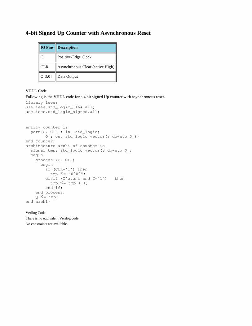
4-bit Signed Up Counter with Asynchronous Reset
IO Pins Description
C Positive-Edge Clock
CLR Asynchronous Clear (active High)
Q[3:0] Data Output
VHDL Code Following is the VHDL code for a 4-bit signed Up counter with asynchronous reset. library ieee; use ieee.std_logic_1164.all; use ieee.std_logic_signed.all; entity counter is port(C, CLR : in std_logic; Q : out std_logic_vector(3 downto 0)); end counter; architecture archi of counter is signal tmp: std_logic_vector(3 downto 0); begin process (C, CLR) begin if (CLR='1') then tmp = "0000"; elsif (C'event and C='1') then tmp = tmp + 1; end if; end process; Q = tmp; end archi; Verilog Code There is no equivalent Verilog code. No constraints are available.
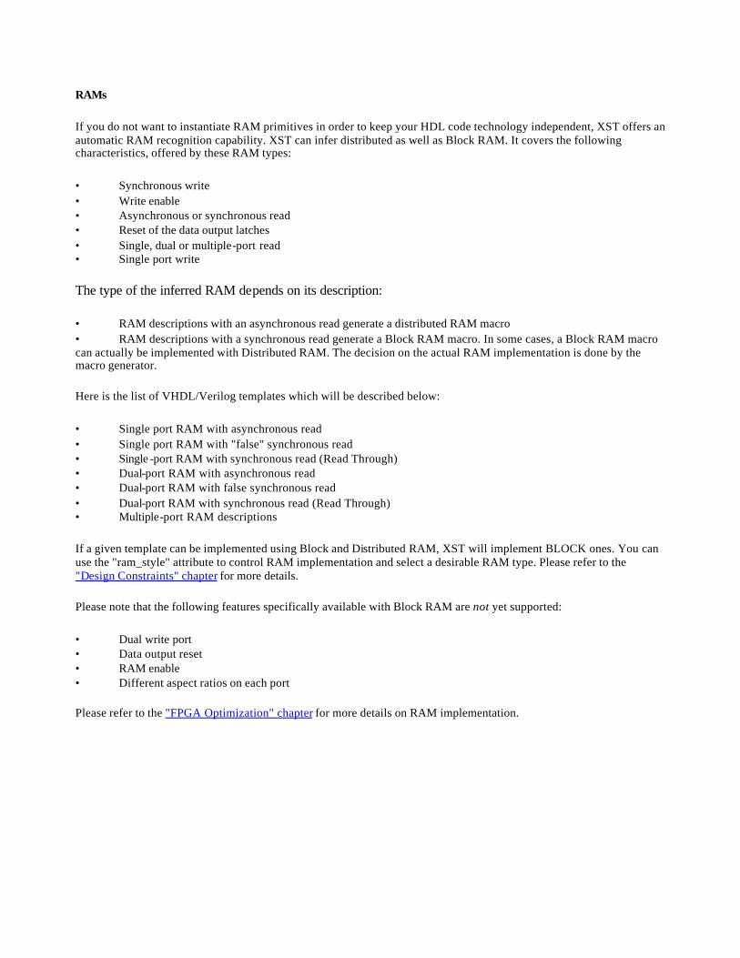
RAMs
If you do not want to instantiate RAM primitives in order to keep your HDL code technology independent, XST offers an automatic RAM recognition capability. XST can infer distributed as well as Block RAM. It covers the following characteristics, offered by these RAM types:
• Synchronous write • Write enable • Asynchronous or synchronous read • Reset of the data output latches • Single, dual or multiple-port read • Single port write
The type of the inferred RAM depends on its description:
• RAM descriptions with an asynchronous read generate a distributed RAM macro • RAM descriptions with a synchronous read generate a Block RAM macro. In some cases, a Block RAM macro can actually be implemented with Distributed RAM. The decision on the actual RAM implementation is done by the macro generator.
Here is the list of VHDL/Verilog templates which will be described below:
• Single port RAM with asynchronous read • Single port RAM with "false" synchronous read • Single -port RAM with synchronous read (Read Through) • Dual-port RAM with asynchronous read • Dual-port RAM with false synchronous read • Dual-port RAM with synchronous read (Read Through) • Multiple-port RAM descriptions
If a given template can be implemented using Block and Distributed RAM, XST will implement BLOCK ones. You can use the "ram_style" attribute to control RAM implementation and select a desirable RAM type. Please refer to the "Design Constraints" chapter for more details.
Please note that the following features specifically available with Block RAM are not yet supported:
• Dual write port • Data output reset • RAM enable • Different aspect ratios on each port
Please refer to the "FPGA Optimization" chapter for more details on RAM implementation.
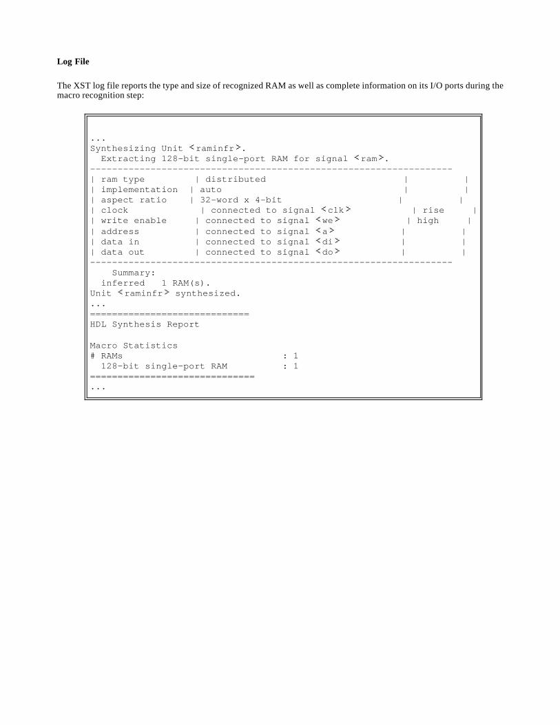
Log File
The XST log file reports the type and size of recognized RAM as well as complete information on its I/O ports during the macro recognition step:
... Synthesizing Unit raminfr . Extracting 128-bit single-port RAM for signal ram . ------------------------------------------------------------------ | ram type | distributed | | | implementation | auto | | | aspect ratio | 32-word x 4-bit | | | clock | connected to signal clk | rise | | write enable | connected to signal we | high | | address | connected to signal a | | | data in | connected to signal di | | | data out | connected to signal do | | ------------------------------------------------------------------ Summary: inferred 1 RAM(s). Unit raminfr synthesized. ... ============================= HDL Synthesis Report Macro Statistics # RAMs : 1 128-bit single-port RAM : 1 ============================== ...
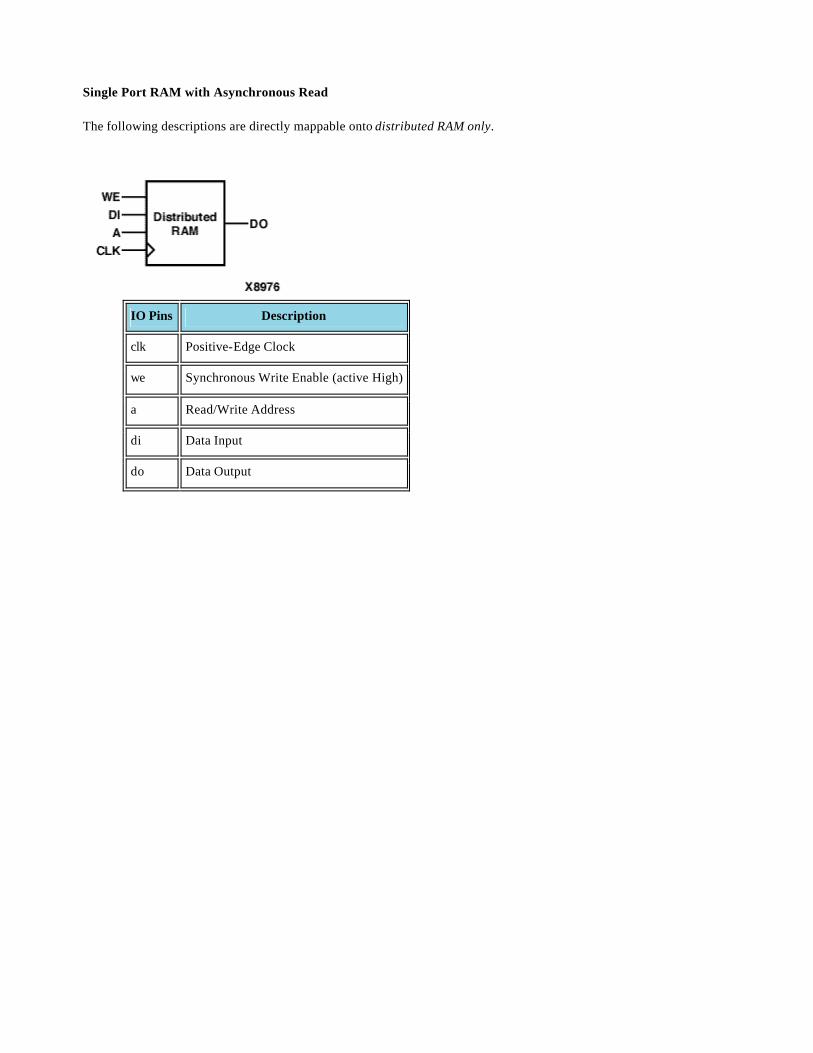
Single Port RAM with Asynchronous Read
The following descriptions are directly mappable onto distributed RAM only.
IO Pins Description
clk Positive-Edge Clock
we Synchronous Write Enable (active High)
a Read/Write Address
di Data Input
do Data Output
VHDL
Following is the VHDL code for a single port RAM with asynchronous read.
library ieee; use ieee.std_logic_1164.all; use ieee.std_logic_unsigned.all; entity raminfr is port (clk : in std_logic; we : in std_logic; a : in std_logic_vector(4 downto 0); di : in std_logic_vector(3 downto 0); do : out std_logic_vector(3 downto 0)); end raminfr; architecture syn of raminfr is type ram_type is array (31 downto 0) of std_logic_vector (3 downto 0); signal RAM : ram_type; begin process (clk) begin if (clk'event and clk = '1') then if (we = '1') then RAM(conv_integer(a)) = di; end if; end if; end process; do = RAM(conv_integer(a)); end syn;
Verilog
Following is the Verilog code for a single port RAM with asynchronous read.
module raminfr (clk, we, a, di, do); input clk; input we; input [4:0] a; input [3:0] di; output [3:0] do; reg [3:0] ram [31:0]; always @(posedge clk) begin if (we) ram[a] = di; end assign do = ram[a]; endmodule
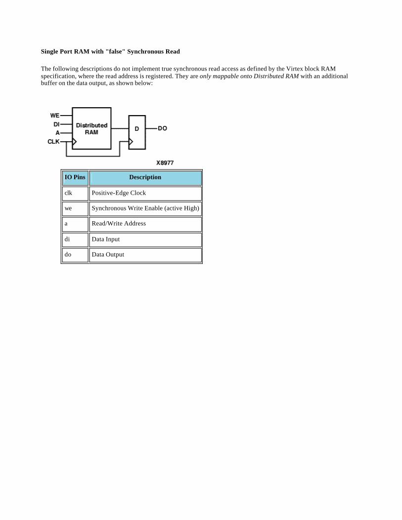
Single Port RAM with "false" Synchronous Read
The following descriptions do not implement true synchronous read access as defined by the Virtex block RAM specification, where the read address is registered. They are only mappable onto Distributed RAM with an additional buffer on the data output, as shown below:
IO Pins Description
clk Positive-Edge Clock
we Synchronous Write Enable (active High)
a Read/Write Address
di Data Input
do Data Output
VHDL
Following is the VHDL code for a single port RAM with "false" synchronous read.
library ieee; use ieee.std_logic_1164.all; use ieee.std_logic_unsigned.all; entity raminfr is port (clk : in std_logic; we : in std_logic; a : in std_logic_vector(4 downto 0); di : in std_logic_vector(3 downto 0); do : out std_logic_vector(3 downto 0)); end raminfr; architecture syn of raminfr is type ram_type is array (31 downto 0) of std_logic_vector (3 downto 0); signal RAM : ram_type; begin process (clk) begin if (clk'event and clk = '1') then if (we = '1') then RAM(conv_integer(a)) = di; end if; do = RAM(conv_integer(a)); end if; end process; end syn
Verilog
Following is the Verilog code for a single port RAM with "false" synchronous read.
module raminfr (clk, we, a, di, do); input clk; input we; input [4:0] a; input [3:0] di; output [3:0] do; reg [3:0] ram [31:0]; reg [3:0] do; always @(posedge clk) begin if (we) ram[a] = di; do = ram[a]; end endmodule
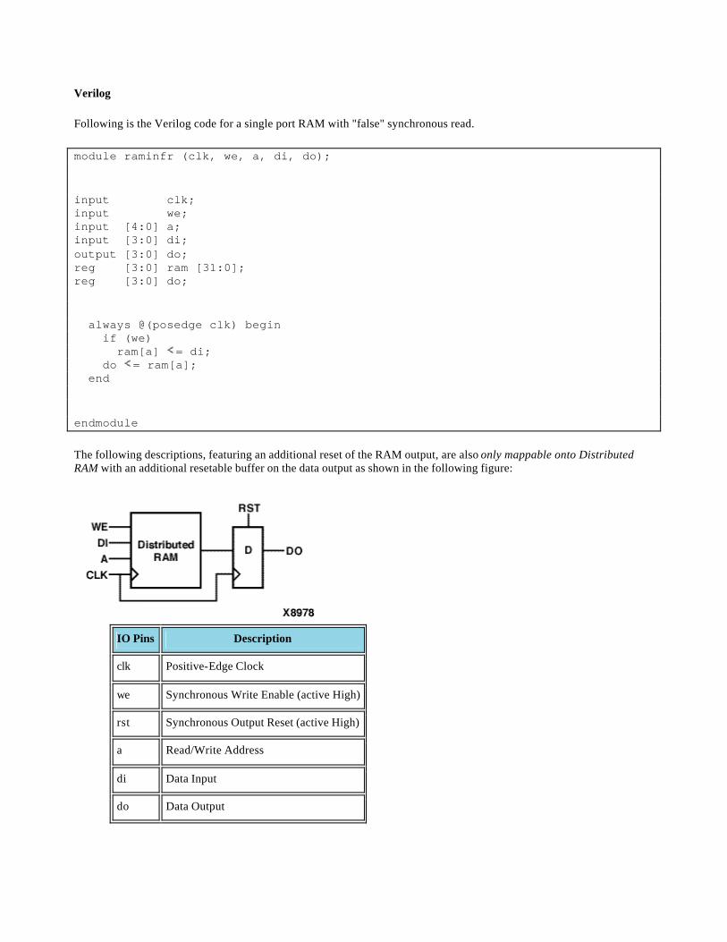
The following descriptions, featuring an additional reset of the RAM output, are also only mappable onto Distributed RAM with an additional resetable buffer on the data output as shown in the following figure:
IO Pins Description
clk Positive-Edge Clock
we Synchronous Write Enable (active High)
rst Synchronous Output Reset (active High)
a Read/Write Address
di Data Input
do Data Output
VHDL
Following is the VHDL code.
library ieee; use ieee.std_logic_1164.all; use ieee.std_logic_unsigned.all; entity raminfr is port (clk : in std_logic; we : in std_logic; rst : in std_logic; a : in std_logic_vector(4 downto 0); di : in std_logic_vector(3 downto 0); do : out std_logic_vector(3 downto 0)); end raminfr; architecture syn of raminfr is type ram_type is array (31 downto 0) of std_logic_vector (3 downto 0); signal RAM : ram_type; begin process (clk) begin if (clk'event and clk = '1') then if (we = '1') then RAM(conv_integer(a)) = di; end if; if (rst = '1') then do = (others = '0'); else do = RAM(conv_integer(a)); end if; end if; end process; end syn;
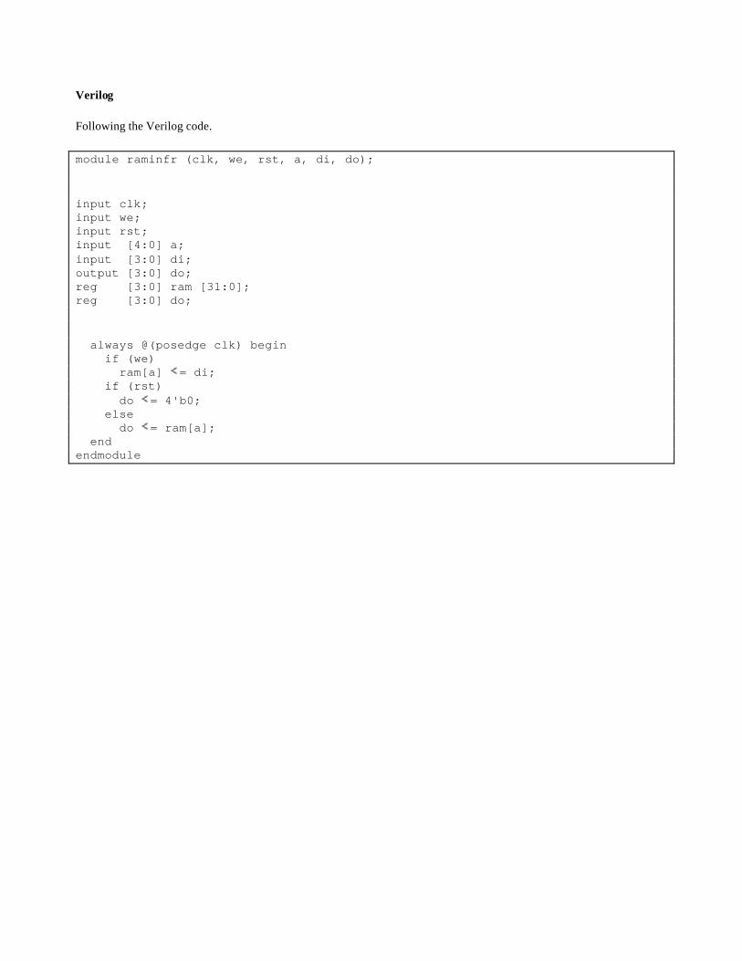
Verilog
Following the Verilog code.
module raminfr (clk, we, rst, a, di, do); input clk; input we; input rst; input [4:0] a; input [3:0] di; output [3:0] do; reg [3:0] ram [31:0]; reg [3:0] do; always @(posedge clk) begin if (we) ram[a] = di; if (rst) do = 4'b0; else do = ram[a]; end endmodule
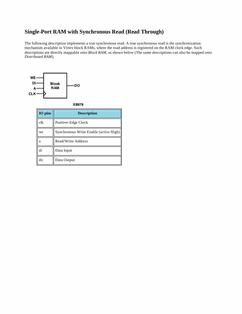
Single-Port RAM with Synchronous Read (Read Through)
The following description implements a true synchronous read. A true synchronous read is the synchronization mechanism available in Virtex block RAMs, where the read address is registered on the RAM clock edge. Such descriptions are directly mappable onto Block RAM, as shown below (The same descriptions can also be mapped onto Distributed RAM).
IO pins Description
clk Positive-Edge Clock
we Synchronous Write Enable (active High)
a Read/Write Address
di Data Input
do Data Output
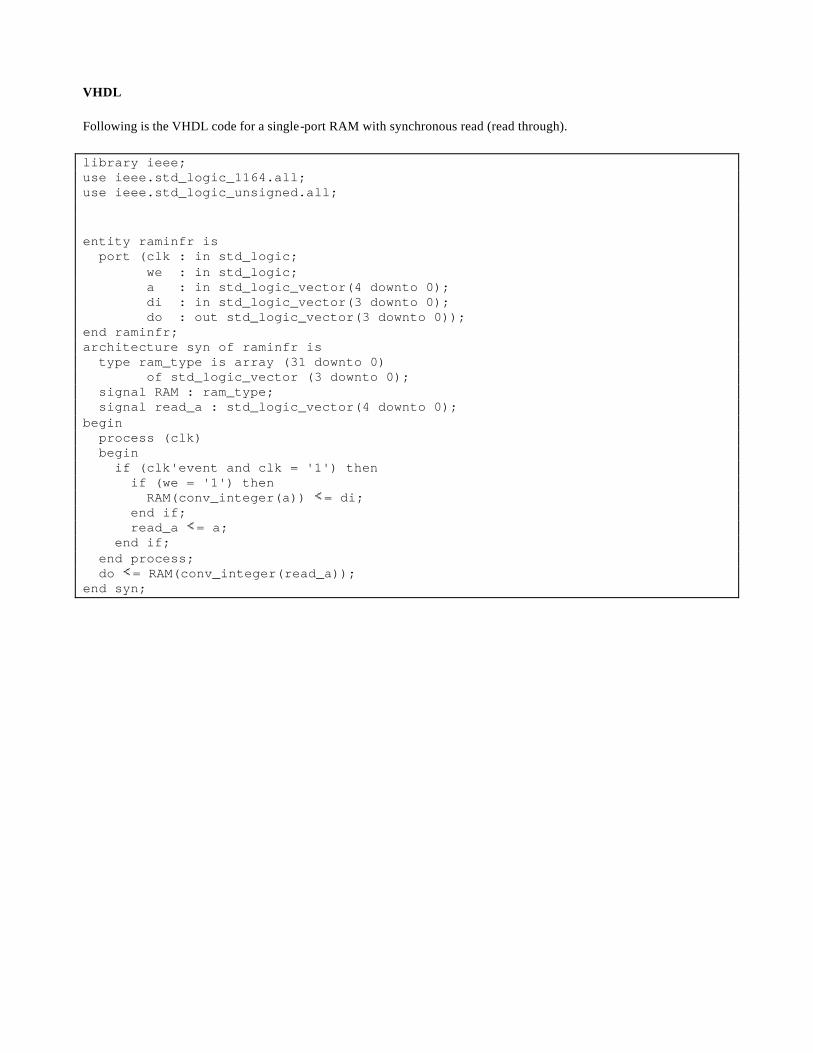
VHDL
Following is the VHDL code for a single-port RAM with synchronous read (read through).
library ieee; use ieee.std_logic_1164.all; use ieee.std_logic_unsigned.all; entity raminfr is port (clk : in std_logic; we : in std_logic; a : in std_logic_vector(4 downto 0); di : in std_logic_vector(3 downto 0); do : out std_logic_vector(3 downto 0)); end raminfr; architecture syn of raminfr is type ram_type is array (31 downto 0) of std_logic_vector (3 downto 0); signal RAM : ram_type; signal read_a : std_logic_vector(4 downto 0); begin process (clk) begin if (clk'event and clk = '1') then if (we = '1') then RAM(conv_integer(a)) = di; end if; read_a = a; end if; end process; do = RAM(conv_integer(read_a)); end syn;
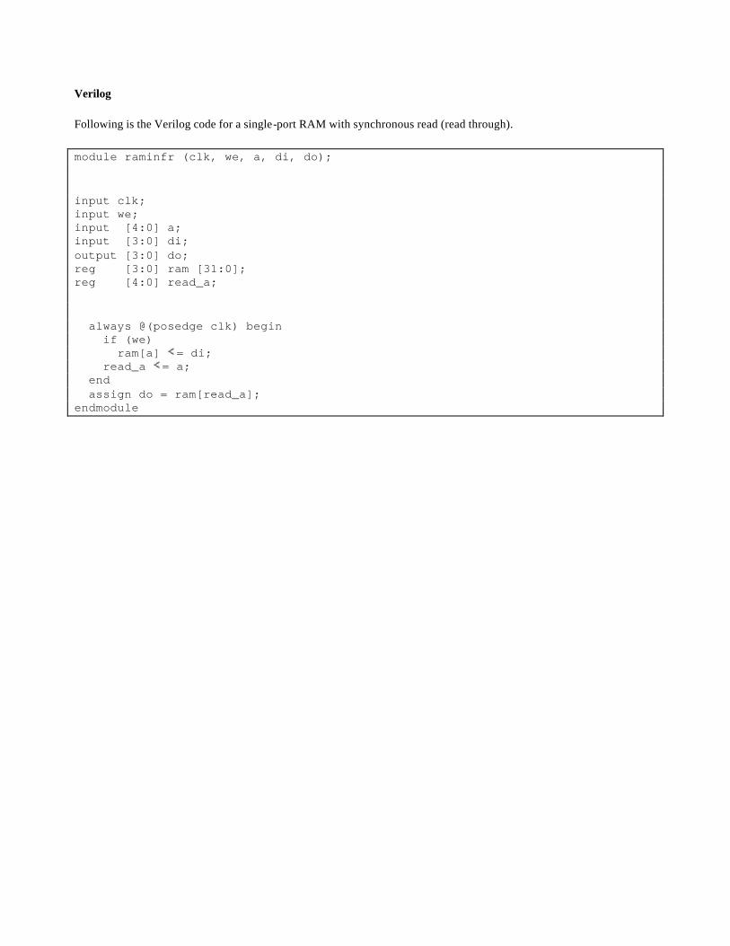
Verilog
Following is the Verilog code for a single-port RAM with synchronous read (read through).
module raminfr (clk, we, a, di, do); input clk; input we; input [4:0] a; input [3:0] di; output [3:0] do; reg [3:0] ram [31:0]; reg [4:0] read_a; always @(posedge clk) begin if (we) ram[a] = di; read_a = a; end assign do = ram[read_a]; endmodule
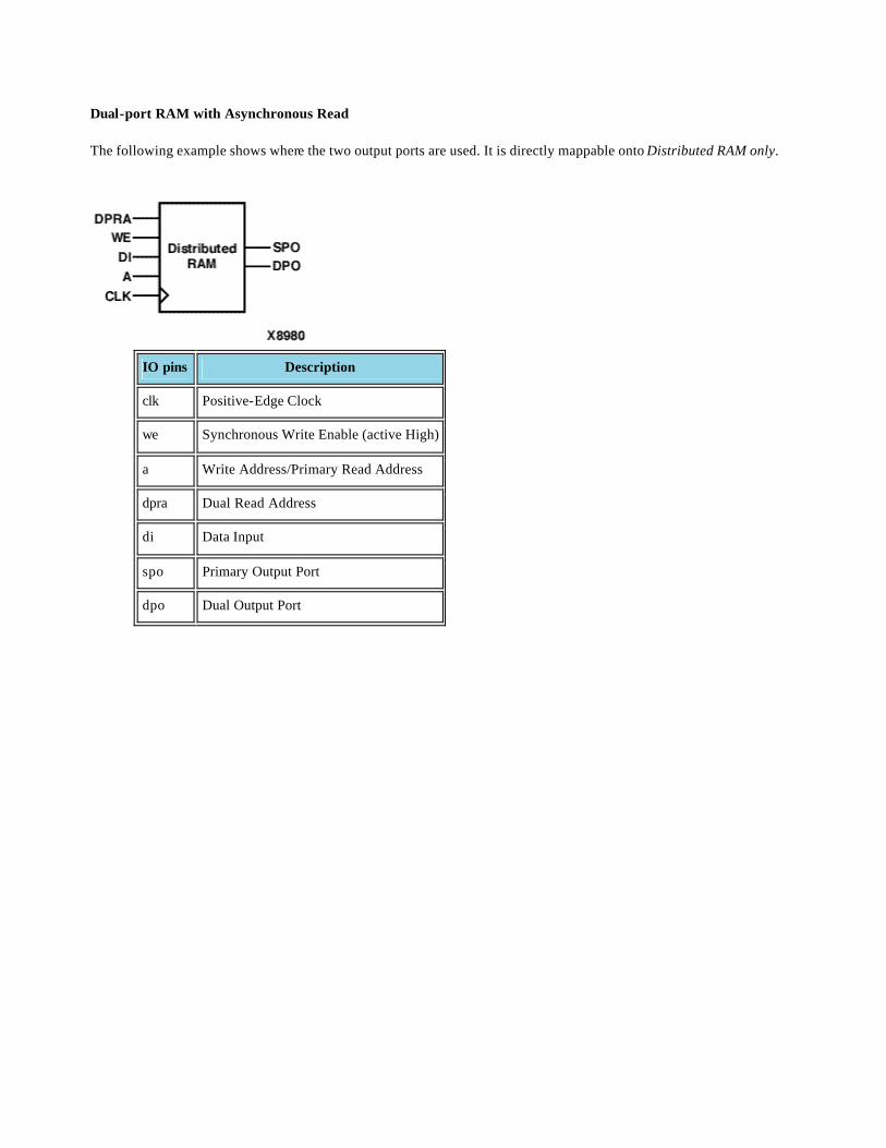
Dual-port RAM with Asynchronous Read
The following example shows where the two output ports are used. It is directly mappable onto Distributed RAM only.
IO pins Description
clk Positive-Edge Clock
we Synchronous Write Enable (active High)
a Write Address/Primary Read Address
dpra Dual Read Address
di Data Input
spo Primary Output Port
dpo Dual Output Port
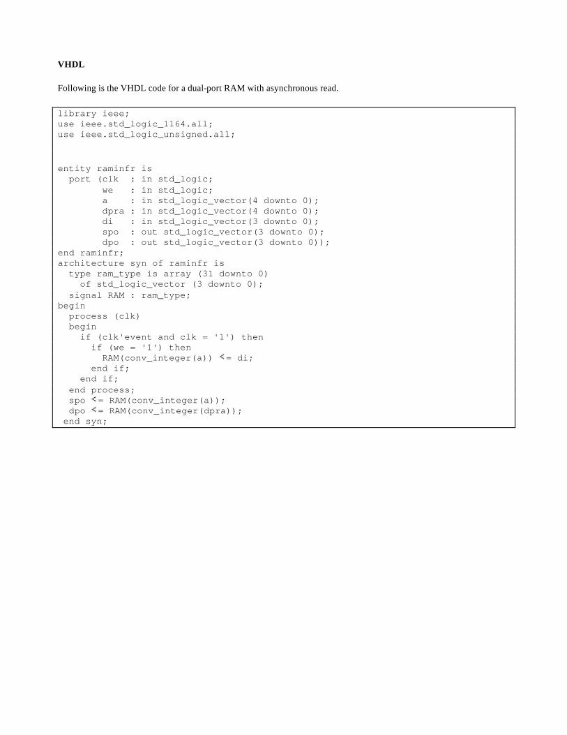
VHDL
Following is the VHDL code for a dual-port RAM with asynchronous read.
library ieee; use ieee.std_logic_1164.all; use ieee.std_logic_unsigned.all; entity raminfr is port (clk : in std_logic; we : in std_logic; a : in std_logic_vector(4 downto 0); dpra : in std_logic_vector(4 downto 0); di : in std_logic_vector(3 downto 0); spo : out std_logic_vector(3 downto 0); dpo : out std_logic_vector(3 downto 0)); end raminfr; architecture syn of raminfr is type ram_type is array (31 downto 0) of std_logic_vector (3 downto 0); signal RAM : ram_type; begin process (clk) begin if (clk'event and clk = '1') then if (we = '1') then RAM(conv_integer(a)) = di; end if; end if; end process; spo = RAM(conv_integer(a)); dpo = RAM(conv_integer(dpra)); end syn;
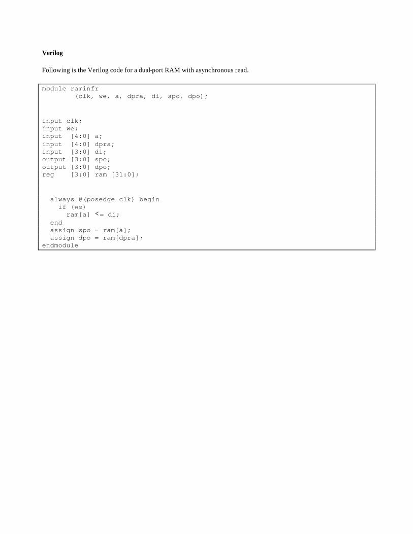
Verilog
Following is the Verilog code for a dual-port RAM with asynchronous read.
module raminfr (clk, we, a, dpra, di, spo, dpo); input clk; input we; input [4:0] a; input [4:0] dpra; input [3:0] di; output [3:0] spo; output [3:0] dpo; reg [3:0] ram [31:0]; always @(posedge clk) begin if (we) ram[a] = di; end assign spo = ram[a]; assign dpo = ram[dpra]; endmodule
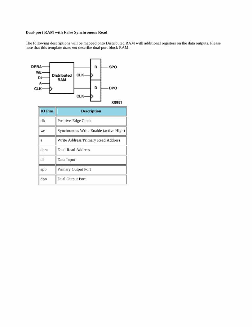
Dual-port RAM with False Synchronous Read
The following descriptions will be mapped onto Distributed RAM with additional registers on the data outputs. Please note that this template does not describe dual-port block RAM.
IO Pins Description
clk Positive-Edge Clock
we Synchronous Write Enable (active High)
a Write Address/Primary Read Address
dpra Dual Read Address
di Data Input
spo Primary Output Port
dpo Dual Output Port
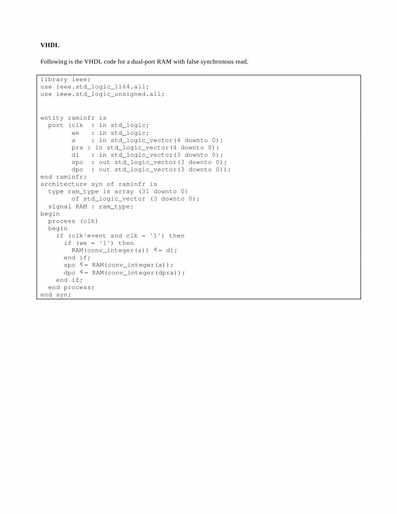
VHDL
Following is the VHDL code for a dual-port RAM with false synchronous read.
library ieee; use ieee.std_logic_1164.all; use ieee.std_logic_unsigned.all; entity raminfr is port (clk : in std_logic; we : in std_logic; a : in std_logic_vector(4 downto 0); pra : in std_logic_vector(4 downto 0); di : in std_logic_vector(3 downto 0); spo : out std_logic_vector(3 downto 0); dpo : out std_logic_vector(3 downto 0)); end raminfr; architecture syn of raminfr is type ram_type is array (31 downto 0) of std_logic_vector (3 downto 0); signal RAM : ram_type; begin process (clk) begin if (clk'event and clk = '1') then if (we = '1') then RAM(conv_integer(a)) = di; end if; spo = RAM(conv_integer(a)); dpo = RAM(conv_integer(dpra)); end if; end process; end syn;
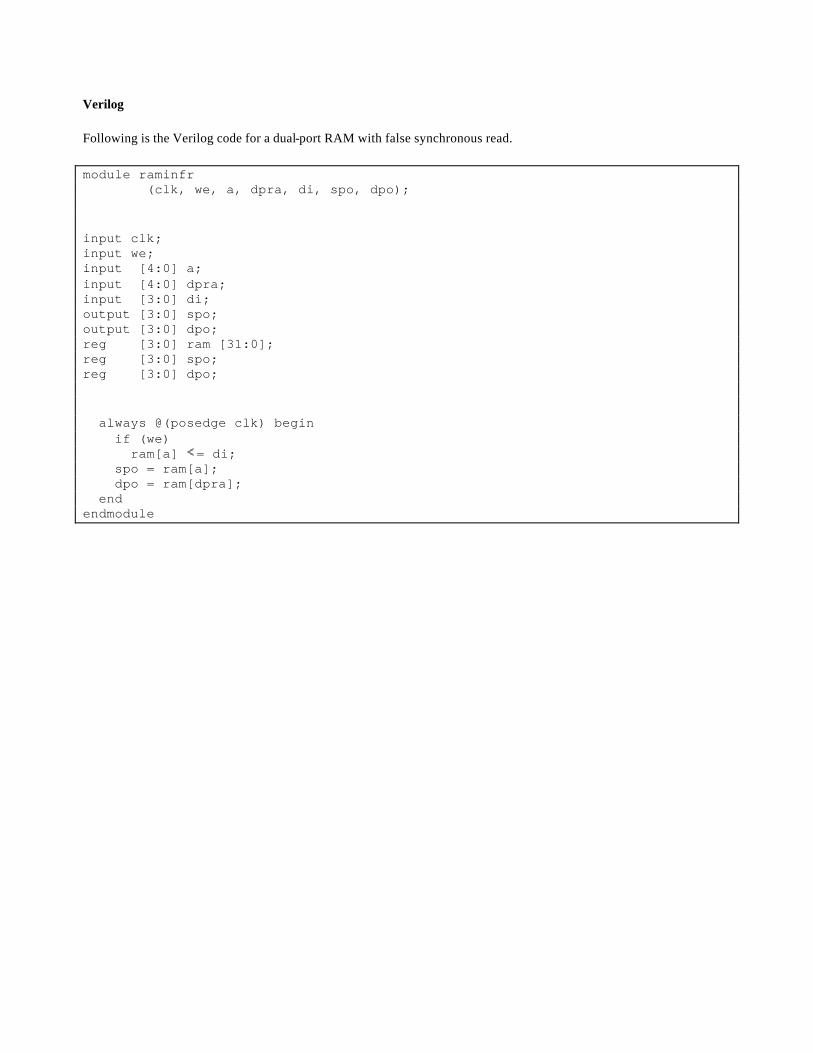
Verilog
Following is the Verilog code for a dual-port RAM with false synchronous read.
module raminfr (clk, we, a, dpra, di, spo, dpo); input clk; input we; input [4:0] a; input [4:0] dpra; input [3:0] di; output [3:0] spo; output [3:0] dpo; reg [3:0] ram [31:0]; reg [3:0] spo; reg [3:0] dpo; always @(posedge clk) begin if (we) ram[a] = di; spo = ram[a]; dpo = ram[dpra]; end endmodule
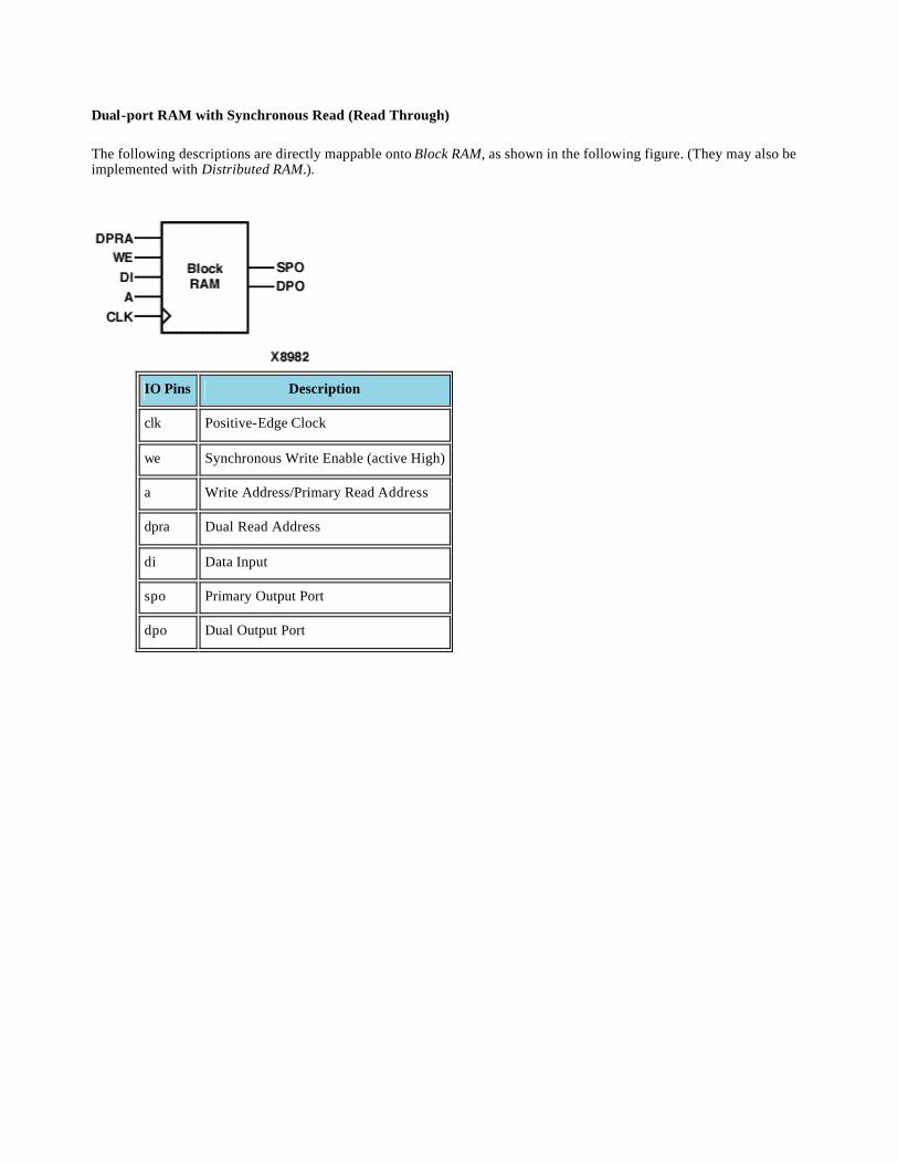
Dual-port RAM with Synchronous Read (Read Through)
The following descriptions are directly mappable onto Block RAM, as shown in the following figure. (They may also be implemented with Distributed RAM.).
IO Pins Description
clk Positive-Edge Clock
we Synchronous Write Enable (active High)
a Write Address/Primary Read Address
dpra Dual Read Address
di Data Input
spo Primary Output Port
dpo Dual Output Port
VHDL
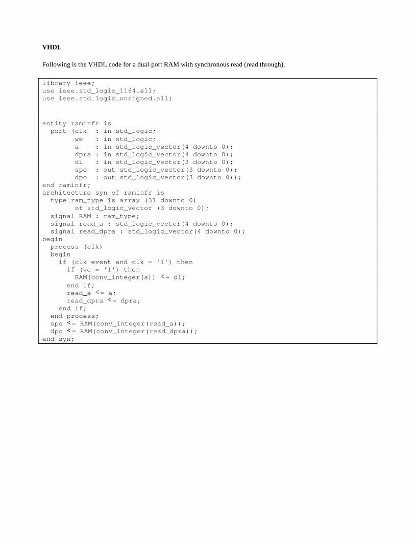
Following is the VHDL code for a dual-port RAM with synchronous read (read through).
library ieee; use ieee.std_logic_1164.all; use ieee.std_logic_unsigned.all; entity raminfr is port (clk : in std_logic; we : in std_logic; a : in std_logic_vector(4 downto 0); dpra : in std_logic_vector(4 downto 0); di : in std_logic_vector(3 downto 0); spo : out std_logic_vector(3 downto 0); dpo : out std_logic_vector(3 downto 0)); end raminfr; architecture syn of raminfr is type ram_type is array (31 downto 0) of std_logic_vector (3 downto 0); signal RAM : ram_type; signal read_a : std_logic_vector(4 downto 0); signal read_dpra : std_logic_vector(4 downto 0); begin process (clk) begin if (clk'event and clk = '1') then if (we = '1') then RAM(conv_integer(a)) = di; end if; read_a = a; read_dpra = dpra; end if; end process; spo = RAM(conv_integer(read_a)); dpo = RAM(conv_integer(read_dpra)); end syn;
Verilog
Following is the Verilog code for a dual-port RAM with synchronous read (read through).
module raminfr (clk, we, a, dpra, di, spo, dpo); input clk; input we; input [4:0] a; input [4:0] dpra; input [3:0] di; output [3:0] spo; output [3:0] dpo; reg [3:0] ram [31:0]; reg [4:0] read_a; reg [4:0] read_dpra; always @(posedge clk) begin if (we) ram[a] = di; read_a = a; read_dpra = dpra; end assign spo = ram[read_a]; assign dpo = ram[read_dpra]; endmodule
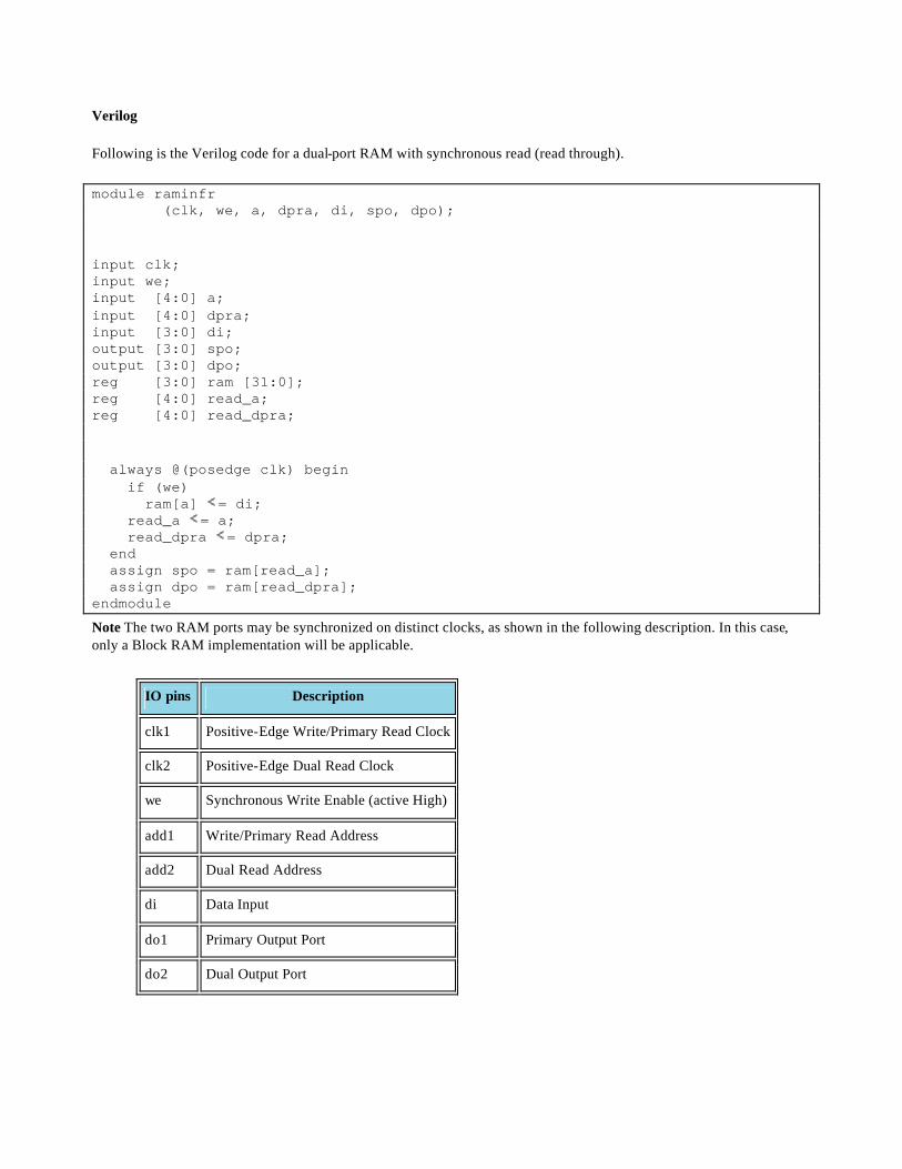
Note The two RAM ports may be synchronized on distinct clocks, as shown in the following description. In this case, only a Block RAM implementation will be applicable.
IO pins Description
clk1 Positive-Edge Write/Primary Read Clock
clk2 Positive-Edge Dual Read Clock
we Synchronous Write Enable (active High)
add1 Write/Primary Read Address
add2 Dual Read Address
di Data Input
do1 Primary Output Port
do2 Dual Output Port
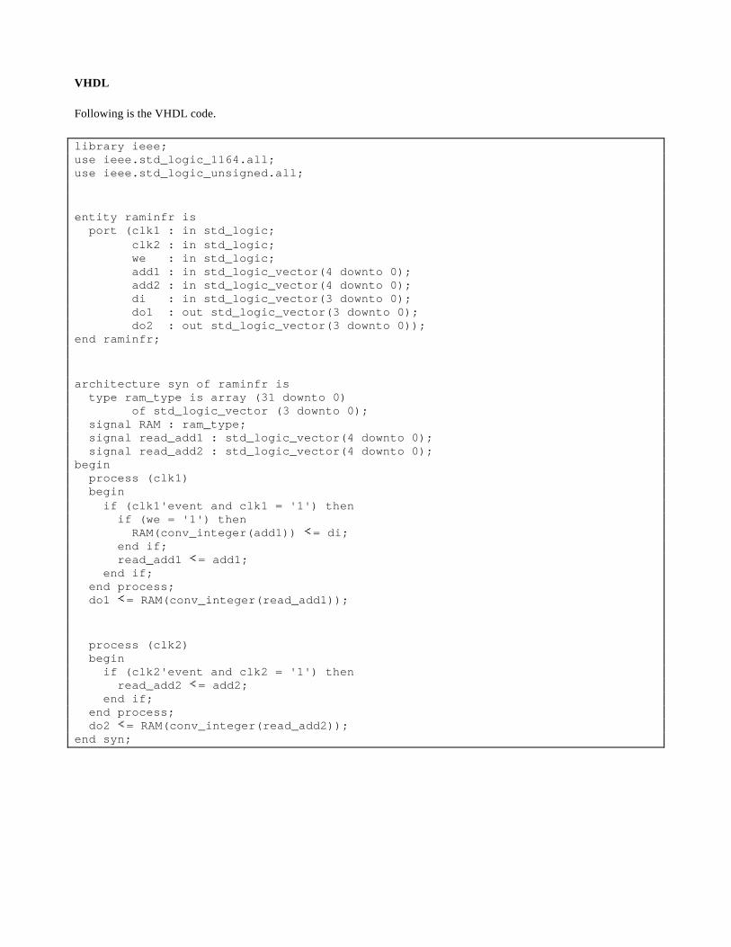
VHDL
Following is the VHDL code.
library ieee; use ieee.std_logic_1164.all; use ieee.std_logic_unsigned.all; entity raminfr is port (clk1 : in std_logic; clk2 : in std_logic; we : in std_logic; add1 : in std_logic_vector(4 downto 0); add2 : in std_logic_vector(4 downto 0); di : in std_logic_vector(3 downto 0); do1 : out std_logic_vector(3 downto 0); do2 : out std_logic_vector(3 downto 0)); end raminfr; architecture syn of raminfr is type ram_type is array (31 downto 0) of std_logic_vector (3 downto 0); signal RAM : ram_type; signal read_add1 : std_logic_vector(4 downto 0); signal read_add2 : std_logic_vector(4 downto 0); begin process (clk1) begin if (clk1'event and clk1 = '1') then if (we = '1') then RAM(conv_integer(add1)) = di; end if; read_add1 = add1; end if; end process; do1 = RAM(conv_integer(read_add1)); process (clk2) begin if (clk2'event and clk2 = '1') then read_add2 = add2; end if; end process; do2 = RAM(conv_integer(read_add2)); end syn;
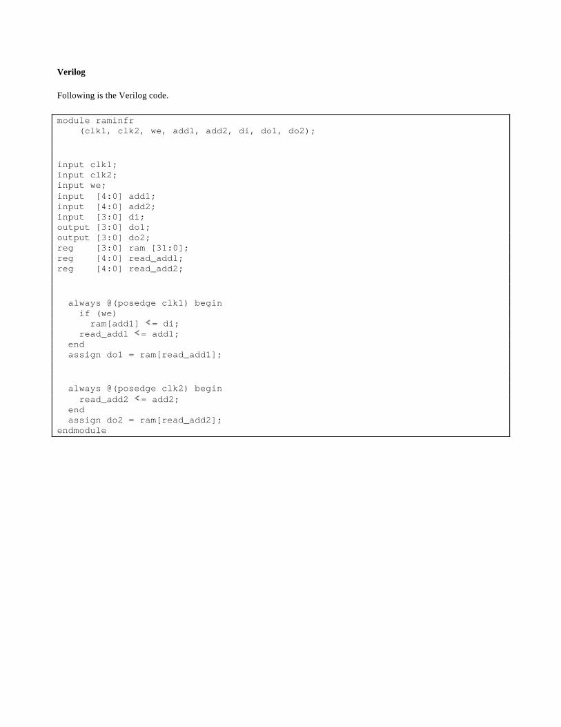
Verilog
Following is the Verilog code.
module raminfr (clk1, clk2, we, add1, add2, di, do1, do2); input clk1; input clk2; input we; input [4:0] add1; input [4:0] add2; input [3:0] di; output [3:0] do1; output [3:0] do2; reg [3:0] ram [31:0]; reg [4:0] read_add1; reg [4:0] read_add2; always @(posedge clk1) begin if (we) ram[add1] = di; read_add1 = add1; end assign do1 = ram[read_add1]; always @(posedge clk2) begin read_add2 = add2; end assign do2 = ram[read_add2]; endmodule
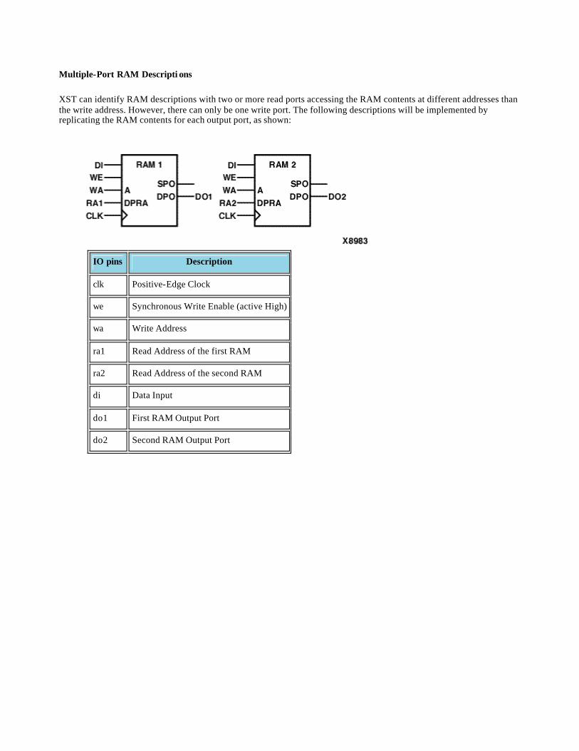
Multiple-Port RAM Descripti ons
XST can identify RAM descriptions with two or more read ports accessing the RAM contents at different addresses than the write address. However, there can only be one write port. The following descriptions will be implemented by replicating the RAM contents for each output port, as shown:
IO pins Description
clk Positive-Edge Clock
we Synchronous Write Enable (active High)
wa Write Address
ra1 Read Address of the first RAM
ra2 Read Address of the second RAM
di Data Input
do1 First RAM Output Port
do2 Second RAM Output Port
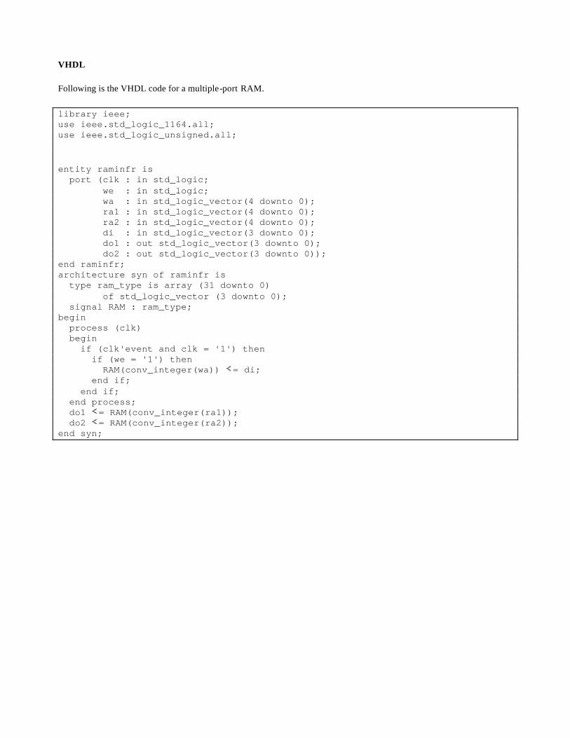
VHDL
Following is the VHDL code for a multiple-port RAM.
library ieee; use ieee.std_logic_1164.all; use ieee.std_logic_unsigned.all; entity raminfr is port (clk : in std_logic; we : in std_logic; wa : in std_logic_vector(4 downto 0); ra1 : in std_logic_vector(4 downto 0); ra2 : in std_logic_vector(4 downto 0); di : in std_logic_vector(3 downto 0); do1 : out std_logic_vector(3 downto 0); do2 : out std_logic_vector(3 downto 0)); end raminfr; architecture syn of raminfr is type ram_type is array (31 downto 0) of std_logic_vector (3 downto 0); signal RAM : ram_type; begin process (clk) begin if (clk'event and clk = '1') then if (we = '1') then RAM(conv_integer(wa)) = di; end if; end if; end process; do1 = RAM(conv_integer(ra1)); do2 = RAM(conv_integer(ra2)); end syn;
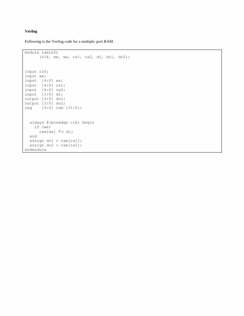
Verilog
Following is the Verilog code for a multiple -port RAM.
module raminfr (clk, we, wa, ra1, ra2, di, do1, do2); input clk; input we; input [4:0] wa; input [4:0] ra1; input [4:0] ra2; input [3:0] di; output [3:0] do1; output [3:0] do2; reg [3:0] ram [31:0]; always @(posedge clk) begin if (we) ram[wa] = di; end assign do1 = ram[ra1]; assign do2 = ram[ra2]; endmodule