Embed Size (px)
Citation preview

PRESENTATION ON “ DESIGN AND ANALYSIS OF
D-FLIP FLOP USING DIFFERENT
TECHNIQUES ”
Submitted By:-Hardeep Kaur
Roll No.1304105
Supervised By: Er. Swarnjeet singh(Asst.Prof.,ECE)

2
TABLE OF CONTENTS
Introduction : D Flip Flop Literature survey Problem formulation Thesis objective Delay in CMOS Power Dissipation in CMOS D Flip Flop Circuit Design , Output waveforms Simulation Results Conclusion Paper publications References

3
INTRODUCTION
Flip flops -:• Flip-flops, also called bistable gates, are digital logic
circuits.• Flip-flops maintain their state until an input pulse called a
trigger is received. When a trigger is received, the flip-flop outputs change state according to defined rules and remain in those states until another trigger is received.
• There are several different kinds of flip-flop circuits such as T (toggle), S-R (set/reset) J-K and D (delay).
• A flip-flop typically includes one or two input signals as well as a clock signal and an output signal..

D Flip flop -: It is also known as a "data" or "delay" flip-flop. The D flip-flop captures the value of the D-input at a definite portion of the clock cycle. That captured value becomes the Q output. At other times, the output Q does not change.
Clock D Qnext
Rising edge 0 0
Rising edge 1 1
Non-Rising X Q

Applications of Flip flops -: • Flip flops are used to design registers and counters. • Registers basic function is to hold information. • Counters basic function is to produce a specified output pattern• sequence. • FPGA contains edge triggered flip flops. D flip flops are also used in finite state machines.

Literature Review
1. Vladimir stojanovic and Vojin G. Oklobdizija,”Comparative Analysis of Master slave latches and flip flops for high performance and low power system”, had proposed a set of rules for consistent estimation of the real performance and power features of the flip-flop and master–slave latch structures. A new simulation and optimization approach is presented, targeting both high performance and power budget issues. Among different single-ended design styles, their work has stated as the most suitable for low-power applications.
2. Mohamed Elgamel et.all,”Noise tolerant low power TSPCL D flip flops,” has proposes a technique to achieve low energy consumption in tspcl d flip flops using 180nm technology.These flip flops has low transistor count thus are small in area.low power was achevied by reducing the swiching activity at some internal nodes.

3. Arkadiy Morgenshtein¹, Alexander Fish² and Israel A. Wagner , “An efficient implementation of D flip flop using The GDI Technique” In this an optimization procedure was developed for GDI DFF, based on iterative transistor sizing, while targeting a minimal power-delay product. A variety of circuits have been implemented in 0.35μm and 0.18μm technologies to compare the proposed GDI structure with a set of representative flip-flops.
4. Ahmed Sayed and Hussain Al.Asaad,’’A new low power high performance flip flop” in this paper they delve into detail of flip flop design and optimization of low power. Also compare the lowest power flip flops of different technologies.
5. N.Vishnu Pradhan et.all,” GDI based low power subthreshold D Flip flop”, In this a digital logic subthreshold operation is introduced to achieve high energy savings.subtthreshold operation is suited for circuits which have low frequency requirments. In this an improved design is GDI MUX is also proposed.

6. Sameer Gull Alie et.al,”Power and delay optimized edge triggered flip flop for low power microcontrollers,” In this paper, a novel highly efficient power and delay optimized True Single Phase clocked (TPSC) edge triggered flip-flop has been proposed. The proposed circuit uses lesser number of transistors than the conventional transmission gate D flip-flop that reduce the overall power and delay. The proposed design is also free from both glitch and charge sharing problems making it suitable for high speed and low power applications. The circuits are simulated in TANNER EDA simulation tool using 180nm technology files to compare the performance of proposed circuit with the existing ones.

Problem Formulation
As per literature review, we consider that the Power has become a burning issue in modern VLSI design. Moreover, power consumed by clocking has taken a major part whole design. To deal with the difficulty efficiently, we have proposed several techniques to design flip flop , and also reduce its other parameters like Delay and Area.

THESIS OBJECTIVE1. In this thesis work, D - Flip flop is designed and simulated using
different techniques like Complementary Metal Oxide Semiconductor static(CMOS), C2MOS, Gate Diffusion input (GDI), Transmission Gate (TG), GDI MUX,TSPC and POWER PC at 180nm &130nm .
2. After that, comparison of these different techniques is done in terms of no. of transistors, delay and power dissipation.
3. The main goal is to find the right logic style for high speed and low power dissipation.

DELAY DEFINITIONS
Rise Time (tr) : Time for the waveform to rise from 10 % to 90% of its steady state value.
Fall Time (tf) : Time for the waveform to fall from 90 % to 10% of its steady state value.
Delay Time (td) : Time difference between input transition(50%) and the 50 % output level.

POWER DISSIPATION IN CMOS CIRCUITS
The total power in a CMOS circuit is given by
Ptotal = Pd + Psc + Ps
where Pd is the Dynamic power dissipation,
Psc is the Short circuit power and Ps is the Static power dissipation.
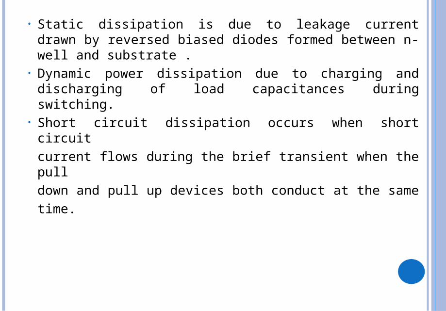
• Static dissipation is due to leakage current drawn by reversed biased diodes formed between n- well and substrate .
• Dynamic power dissipation due to charging and discharging of load capacitances during switching.
• Short circuit dissipation occurs when short circuit
current flows during the brief transient when the pull
down and pull up devices both conduct at the same
time.

LOGICAL OPERATION OF SWITCHES
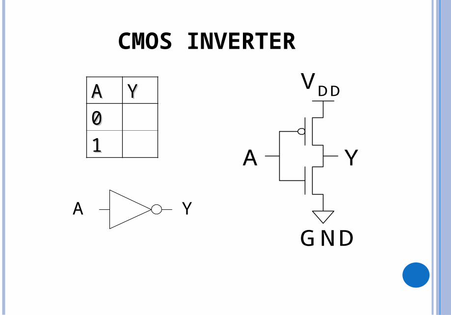
CMOS INVERTER
A Y
AA YY
00
11
VDD
A Y
GND
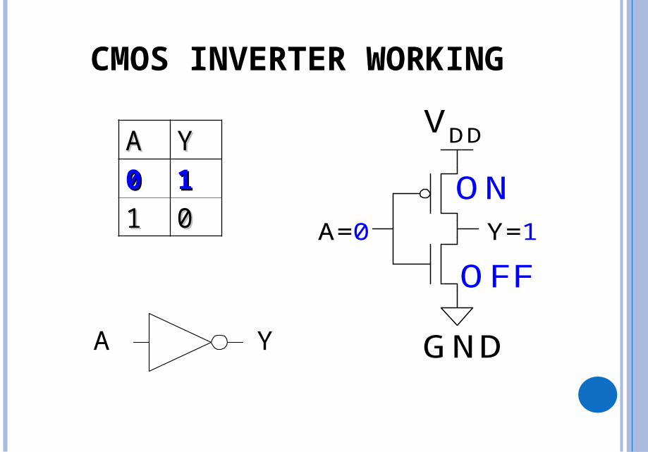
CMOS INVERTER WORKING
AA YY
00 11
11 00
VDD
A=0 Y=1
GND
OFF
ON
A Y

CMOS INVERTER WORKING
VDD
A=1 Y=0
GND
ON
OFF
AA YY
00
11 00
A Y

D FLIP FLOPDESIGN
TECHNIQUES

CONVENTIONAL STATIC CMOS LOGIC
Conventional Static CMOS logic consists of nMOS pull-down and pMOS pull-up transistors together in a complementary way. The simplest CMOS circuit, a logic inverter, requires only one of each type of transistor. CSL has good noise margin, fast speed, low power consumption and easier to design.
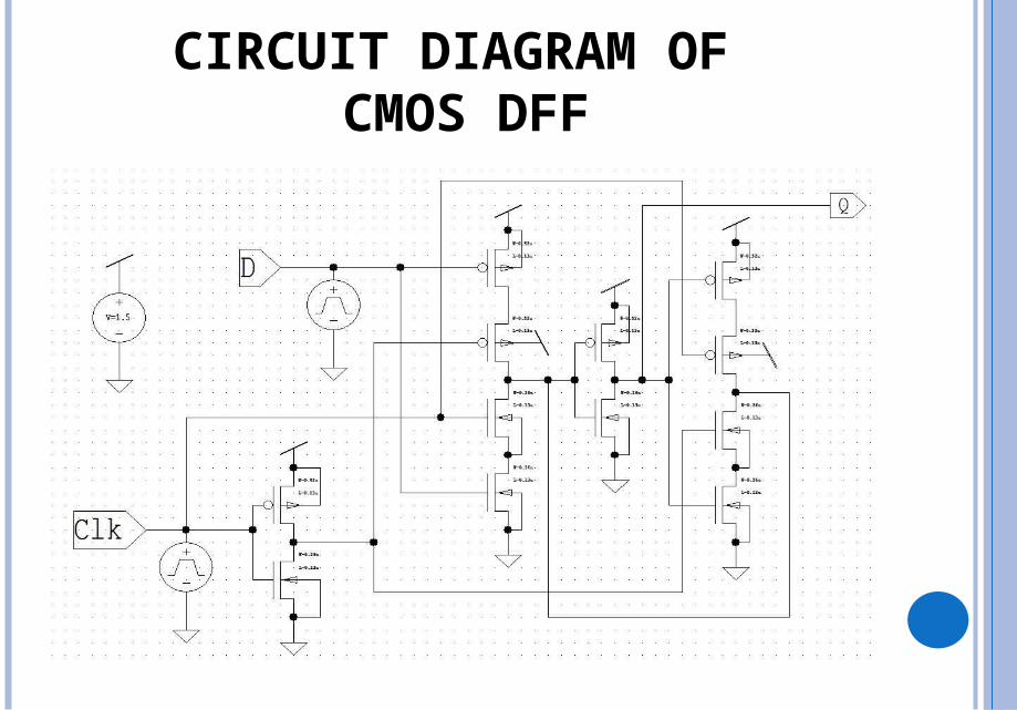
CIRCUIT DIAGRAM OF CMOS DFF

CMOS DFF OUTPUT WAVEFORM

CLOCKED CMOS DFF (C2MOS)
C2MOS is composed of a static logic circuit with tri-state output network (made up of FETs M1 and M2) that is controlled by and
» When , both M1 and M2 are active, and become to a standard static logic gate
» When , both M1 and M2 are cutoff, so the output is a Hi-Z state
01

CIRCUIT DIAGRAM OF C2MOS DFF

C2MOS DFF OUTPUT WAVEFORM
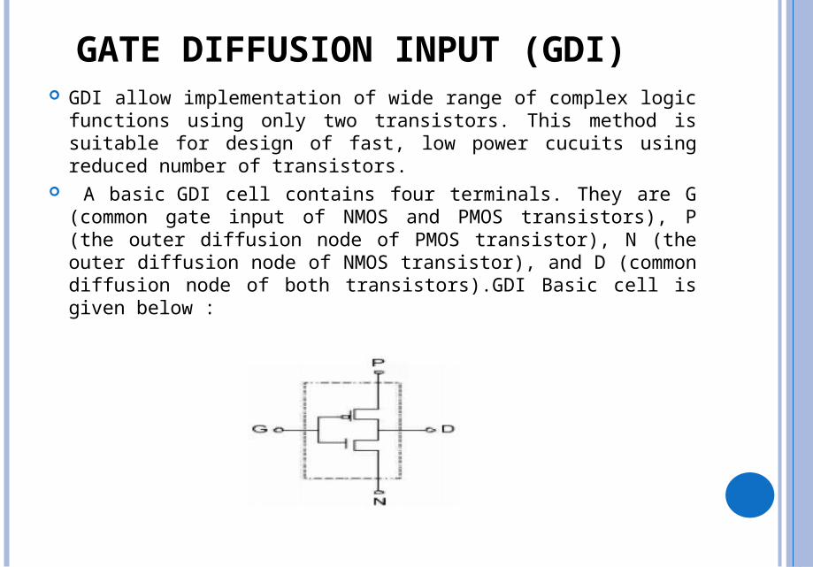
GATE DIFFUSION INPUT (GDI) GDI allow implementation of wide range of complex logic functions
using only two transistors. This method is suitable for design of fast, low power cucuits using reduced number of transistors.
A basic GDI cell contains four terminals. They are G (common gate input of NMOS and PMOS transistors), P (the outer diffusion node of PMOS transistor), N (the outer diffusion node of NMOS transistor), and D (common diffusion node of both transistors).GDI Basic cell is given below :

CIRCUIT DIAGRAM OF GATE DIFFUSION INPUT ( GDI) DFF

OUTPUT WAVEFORM OF GATE DIFFUSION INPUT ( GDI)
DFF

GATE DIFFUSION INPUT ( GDI) MUX DFF
GDI multiplexors are composed of single pair of transistors and a cross coupled pair of inverters. First multiplexer is connected to the system clock and its inputs are connected to the D input and feedback loop. The inverted signal is the input to the second latch , with the feedback loop connected to the opposite input of the second multiplexer .This topology creates a positive edge triggered flip flop with a reduced propagation delay due to single inversion required before the output Q is ready.

CIRCUIT DIGARM OF GATE DIFFUSION INPUT ( GDI) MUX
DFF

OUTPUT WAVEFORM OF GATE DIFFUSION INPUT ( GDI) MUX DFF

TRANSMISSION GATE
A CMOS transmission gate can be constructed by parallel combination of NMOS and PMOS transistors, with complementary gate signals.
The main advantage of transmission gate compared to NMOS transmission gate is to allow the input signal to be transmitted to the output without the threshold voltage attenuation. The schematic diagram of transmission gate is shown below :

CIRCUIT DIGARM OF TRANSMISSION GATE DFF

OUTPUT WAVEFORM OF TRANSMISSION GATE DFF

POWERPC DFF
Main advantages of PowerPC DFF, are short direct path and low-power feedback. Its big clock load greatly influences the total power consumption on chip.

CIRCUIT DIAGRAM OF POWERPC DFF

OUTPUT WAVEFORM OF POWERPC DFF

TRUE SINGLE PHASED CLOCKED (TSPC )DFF
In true single phased clocked logic we have only clock and do not need an inverted clock. This technique eliminated skew problems due to different clock phases. The TSPC logic style was introduced to overcome the complexity of the circuit.

CIRCUIT DIAGRAM OF TSPC DFF

OUTPUT WAVEFORM OF TSPC DFF

PERFORMANCE ANALYSIS OF DIFFERENT DESIGN STYLES AT
180NMS.No. DESIGN STYLE POWER
DISSIPATION(µW)
PROPAGATION DELAY(nsec)
FIGURE OF MERIT(µ-nJ)
NO. OF TRANSISTORS
1 CMOS 3.2 4.93 15.78 18
2 C2MOS 0.94 4.71 4.43 14
4 GDI 1.06 55.48 58.81 18
5 GDI MUX 2.9 2.73 7.92 12
6 POWER PC 58.14 30 1744.20 20
7 TG 1.06 4.67 4.95 12
8 TSPC 0.77 0.37 0.28 9

PERFORMANCE ANALYSIS OF DIFFERENT DESIGN STYLES AT
130NMS.No. DESIGN STYLE POWER
DISSIPATION(µW)
PROPAGATION DELAY(nsec)
FIGURE OF MERIT(µ-nJ)
NO. OF TRANSISTORS
1 CMOS 2 4.94 9.88 18
2 CCMOS 0.52 4.71 2.4492 14
3 GDI 1.3 55 71.5 18
4 GDI MUX 2.43 2.78 6.7554 12
5 POWER PC 0.09 30 2.7 20
6 TG 1.33 0.001 0.00133 12
7 TSPC 0.53 0.29 0.1537 9

CONCLUTIONS1. It is concluded from Power dissipation comparison that PowerPC has
lowest power dissipation at 130nm but TSPC at 180nm. So it is better
to design a digital system with PowerPC or TSPC where low power
dissipation is required like portable digital systems e.g. laptop.
2. It is concluded from Propagation delay comparison that TG design
style has least propagation delay time at 130nm and TSPC at 180nm.
So it is better to use TG or TSPC logic style to design a system where
fast speed is required. The GDI technique is slowest among all.

3. It is concluded from number of transistors
comparison that TSPC technique requires less number
of transistor to design a system than other two design
styles. So electronics circuits designed using TSPC logic
style will occupy less space on the chip.
4. It is also concluded that TG style has the lowest
power- delay product at 130nm and TSPC at
180nm.Thus TG or TSPC has the best performance in
terms of speed and power dissipation at lower supply
voltages.

PAPER PUBLISHED “A Review On Design and Analysis of D Flip Flop Using Different Technologies” INTERNATIONAL JOURNAL
OF TECHNOLOGY ENHANCEMENTS AND EMERGING ENGINEERING RESEARCH, VOL 3, ISSUE 04 32 ISSN 2347-4289
“Design of Single Edge Triggered D Flip Flop Using GDI Technique” IOSR Journal of Electronics and Communication Engineering (IOSR-JECE) e-ISSN: 2278-2834,p- ISSN: 2278-8735.Volume 10, Issue 2, Ver. II (Mar - Apr.2015), PP 47-50 www.iosrjournals.org
“A Review Article On Design Techniques for Low Power Consumption in a Storage Element” International Journal of Innovative Research in Computer and Communication Engineering (An I SO 3297: 2007 Certified Organization) Vol. 3, Issue 4, April 2015
“Design and Analysis of Storage Element using different Technologies” International Journal of Engineering Technology and Computer Research (IJETCR) Available Online at www.ijetcr.org Volume 3; Issue 2; Page No. 169-171
“Design and Optimization of GDI Based 1-bit Comparator using Reverse Logic” International Journal of Recent Research in Electrical and Electronics Engineering (IJRREEE) Vol. 2, Issue 2, pp: (6-10), Month: April 2015 - June 2015, Available at: www.paperpublications.org
“A Review on Analysis of 4-bit Comparator using Different Full-Adder Logic Style with Different Technologies” International Journal of Engineering Technology and Computer Research (IJETCR) Available Online at www.ijetcr.org Volume 3; Issue 3; May-June; Page No. 25-28

REFERENCES[1] Vladimir Stojanovic and Vojin G. Oklobdzija, “Comparative Analysis of Master–Slave
Latches and Flip-Flops for High-Performance and Low-Power Systems”, IEEE Journal of Solid-state Circuits , Vol. 34, No. 4, 1999
[2] M. Alioto and G. Palumbo, “Modeling and Optimized Design of Current Mode MUX/XOR and D Flip-Flop”, IEEE Transactions on Circuits and Systems,Vol. 47, No. 5, 2000
[3] Morgenshtein, A. Fish, I.A. Wagner, “Gate-Diffusion Input (GDI) – A Power Efficient Method for Digital Combinatorial Circuits,” IEEE Transactions,Vol. 10, No. 5, pp. 566-581, 2002
[4] Po-Hui Yang, Jinn-Shyan Rang and Yi-Ming Wang, “A 1-GHz Low-Power
Transposition Memory Using New Pulse-Clocked D Flip-Flops”, ISCAS,IEEE
International Symposium on Circuits and Systems, 2000
[5] Mohamed Elgamel, Tariek Darvish and Magdy Bayoumi”Noise tolerant low power TSPCL D flip flops”, ICSAS,IEEE,2002
[6] Morgenshtein, A. Fish, I.A. Wagner,”An efficient implementation of D flip flop using GDI Technique,”IEEE,2004
[7] Ahmed Sayed and Hussain Al-Asaad,” A new low power high performance flip flop”,IEEE ,2006
[8] Sagi Fisher,Adam Teman, Dmirity Vaysman, Alexander Gertsman,Orly Yadid Pecht,”Ultra low power subthreshold flip flop design,”IEEE, 2009

[9] Manoj sharma, Dr Arti Noor et.al, “An Area and Power Efficient design of Single EdgeTriggered D-Flip Flop”, International Conference on Advances in Recent Technologies in Communication and Computing, 2009
[10] N.vishnu Vardhan Reddy, C.Leela Mohan and M.Srilakshmi, “GDI Based Subthreshold Low Power D- Flip flop”, International Journal of VLSI and Embedded Systems-IJVES , Vol 04, 2013
[11] Sameer Gull Alie , Ms.Tarana Afrin Chandel and Jehangir Rashid dar,” Power and Delay Optimized Edge Triggered Flip-Flop for low power microcontrollers.” International Journal of Scientific and Research Publications, Volume 4, Issue 5, May 2014

THANK YOU