Embed Size (px)
Citation preview
Power Integrations
5245 Hellyer Avenue, San Jose, CA 95138 USA. Tel: +1 408 414 9200 Fax: +1 408 414 9201
www.powerint.com
Title Reference Design Report for a 2.78 W USB Charger Using LNK613DG
Specification 85 – 265 VAC Input; 5 V, 555 mA Output
Application Low-cost Charger or Adapter
Author Applications Engineering Department
Document Number RDR-157
Date October 28, 2008
Revision 1.1
Summary and Features
• Revolutionary control concept provides very low cost, low part-count solution • Primary-side control eliminates secondary-side control and optocoupler • Provides +/-5% constant voltage (CV) and +/-10% constant current (CC) accuracy
including output cable voltage drop compensation for 26 AWG (0.49 Ω) or 24 AWG (0.3 Ω) cables
Over-temperature protection – tight tolerance (+/-5%) with hysteretic recovery for safe PCB temperatures under all conditions
Auto-restart output short circuit and open-loop protection • EcoSmart® – Easily meets all current international energy efficiency standards –
China (CECP) / CEC / ENERGY STAR 2 / EU CoC No-load input energy consumption: <50 mW at 230 VAC Ultra-low leakage current: <5 µA at 265 VAC input (no Y capacitor required) Design easily meets EN550022 and CISPR-22 Class B EMI with >10 dB margin
• Meets IEC 61000-4-5 Class 3 AC line surge • Meets IEC 61000-4-2 ESD immunity (contact and air discharge at 15 kV) • Meets <5 µA battery discharge requirement
PATENT INFORMATION The products and applications illustrated herein (including transformer construction and circuits external to the products) may be covered by one or more U.S. and foreign patents, or potentially by pending U.S. and foreign patent applications assigned to Power Integrations. A complete list of Power Integrations' patents may be found at www.powerint.com. Power Integrations grants its customers a license under certain patent rights as set forth at <http://www.powerint.com/ip.htm>.
28-Oct-08 RDR-157 – 5.0 V / 2.78 W USB Charger
Page 2 of 40
Power Integrations Tel: +1 408 414 9200 Fax: +1 408 414 9201 www.powerint.com
Table of Contents 1 Introduction.................................................................................................................4 2 Power Supply Specification ........................................................................................6 3 Schematic...................................................................................................................7 Circuit Description..............................................................................................................8
3.1 Input Filter ...........................................................................................................8 3.2 LNK613DG Primary.............................................................................................8 3.3 Output Rectification and Filtering ........................................................................8 3.4 Output Regulation ...............................................................................................9
PCB Layout .....................................................................................................................10 4 Bill of Materials .........................................................................................................12 5 Transformer Specification.........................................................................................13
5.1 Electrical Diagram .............................................................................................13 5.2 Electrical Specifications.....................................................................................13 5.3 Materials............................................................................................................13 5.4 Transformer Build Diagram ...............................................................................14 5.5 Transformer Construction..................................................................................15
6 Design Spreadsheet .................................................................................................16 7 Performance Data ....................................................................................................20
7.1 Full Load Efficiency ...........................................................................................20 7.2 Active Mode Measurement Data .......................................................................21
7.2.1 Energy Star v1.1 / CEC (2008)...................................................................21 7.2.2 Energy Star v2 (April 2008) ........................................................................22
7.3 No-Load Input Power ........................................................................................23 7.4 Regulation .........................................................................................................24
7.4.1 Load and Temperature...............................................................................24 8 Thermal Performance...............................................................................................27 9 Waveforms ...............................................................................................................28
9.1 Drain Voltage and Current, Normal Operation...................................................28 9.2 Output Voltage Start-up Profiles........................................................................28
9.2.1 No-Load Start-up Characteristic.................................................................28 9.2.2 Start-up Characteristic Measured Using a Resistive Load (10 Ω) ..............29
9.3 Start-up Characteristic with a Battery Model as Load........................................30 9.4 Drain Voltage and Current Start-up Profile ........................................................31 Load Transient Response (50% to 100% Load Step) ..................................................32 9.5 Output Ripple Measurements............................................................................33
9.5.1 Ripple Measurement Technique ................................................................33 9.5.2 Measurement Results ................................................................................34
10 Line Surge.............................................................................................................36 11 ESD ......................................................................................................................36
11.1 Single-shot Results ...........................................................................................36 11.2 Free-running Results .........................................................................................36
12 Conducted EMI .....................................................................................................37 13 Revision History ....................................................................................................38
RDR-157 – 5.0 V / 2.78 W USB Charger 28-Oct-08
Page 3 of 40
Power Integrations Tel: +1 408 414 9200 Fax: +1 408 414 9201
www.powerint.com
Important Note: Although this board is designed to satisfy safety isolation requirements, the engineering prototype has not been agency approved. Therefore, all testing should be performed using an isolation transformer to provide the AC input to the prototype board.
28-Oct-08 RDR-157 – 5.0 V / 2.78 W USB Charger
Page 4 of 40
Power Integrations Tel: +1 408 414 9200 Fax: +1 408 414 9201 www.powerint.com
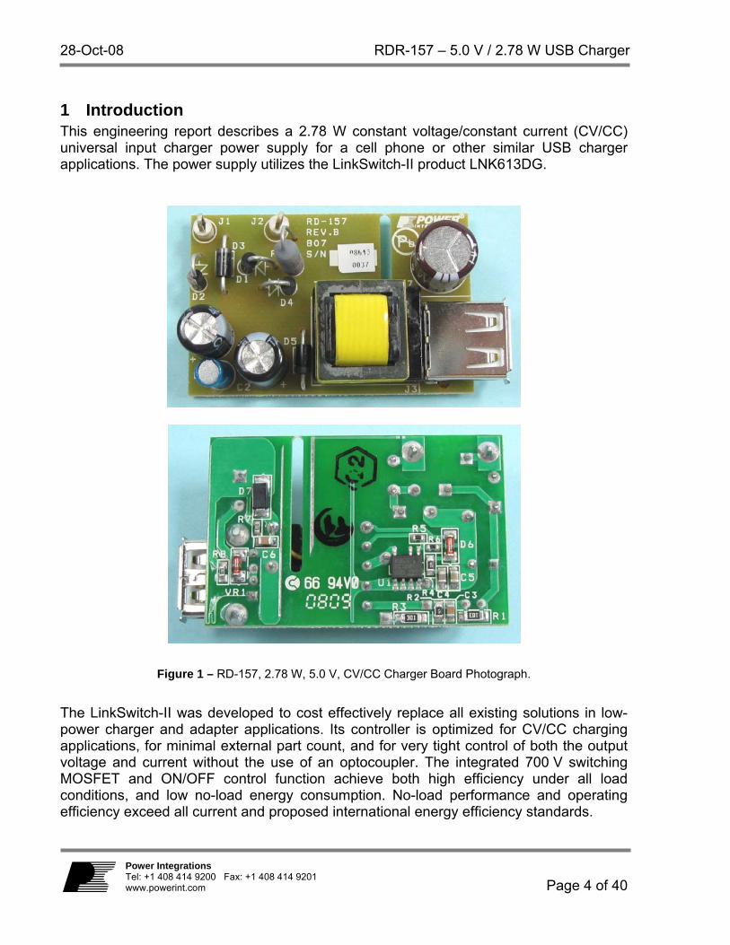
1 Introduction This engineering report describes a 2.78 W constant voltage/constant current (CV/CC) universal input charger power supply for a cell phone or other similar USB charger applications. The power supply utilizes the LinkSwitch-II product LNK613DG.
Figure 1 – RD-157, 2.78 W, 5.0 V, CV/CC Charger Board Photograph.
The LinkSwitch-II was developed to cost effectively replace all existing solutions in low-power charger and adapter applications. Its controller is optimized for CV/CC charging applications, for minimal external part count, and for very tight control of both the output voltage and current without the use of an optocoupler. The integrated 700 V switching MOSFET and ON/OFF control function achieve both high efficiency under all load conditions, and low no-load energy consumption. No-load performance and operating efficiency exceed all current and proposed international energy efficiency standards.
RDR-157 – 5.0 V / 2.78 W USB Charger 28-Oct-08
Page 5 of 40
Power Integrations Tel: +1 408 414 9200 Fax: +1 408 414 9201
www.powerint.com
A unique ON/OFF control scheme provides voltage regulation, as well as support for cable voltage-drop compensation, and tight regulation over a wide temperature range. The output current is regulated by modulating the switching frequency to provide a linear CC characteristic. The LNK613DG controller consists of an oscillator, feedback (sense and logic) circuitry, a 5.8 V regulator, BYPASS (BP) pin programming functions, over-temperature protection, frequency jittering, current-limit circuitry, leading-edge blanking, a frequency controller for CC regulation, and an ON/OFF state machine for CV control. The LNK613DG also provides a sophisticated range of protection features including auto-restart for control loop component open/short circuit faults and output short-circuit conditions. Accurate hysteretic thermal shutdown ensures safe average PCB temperatures under all conditions. The IC package provides extended creepage distance between high and low voltage pins (both at the package and the PCB), which is required in very humid conditions to prevent arcing and to further improve reliability. The LNK613DG can be configured as either self-biased from the high voltage drain pin or supplied via an optional bias supply. When configured as self biased, the very low IC current consumption provides a worst-case no-load power consumption of approximately 200 mW at 265 VAC, well within the 300 mW European Union CoC requirement. When fed from an optional bias supply (as in this design), the no-load power consumption reduces to <40 mW. The EE16 transformer bobbin in this design provides extended creepage to meet safety spacing requirements. Both the EF12.6 and EE13 core sizes could also have been used at this power level. This document contains the power supply specifications, schematic, bill of materials, transformer specifications, and typical performance characteristics for this reference design using the LNK613DG.
28-Oct-08 RDR-157 – 5.0 V / 2.78 W USB Charger
Page 6 of 40
Power Integrations Tel: +1 408 414 9200 Fax: +1 408 414 9201 www.powerint.com
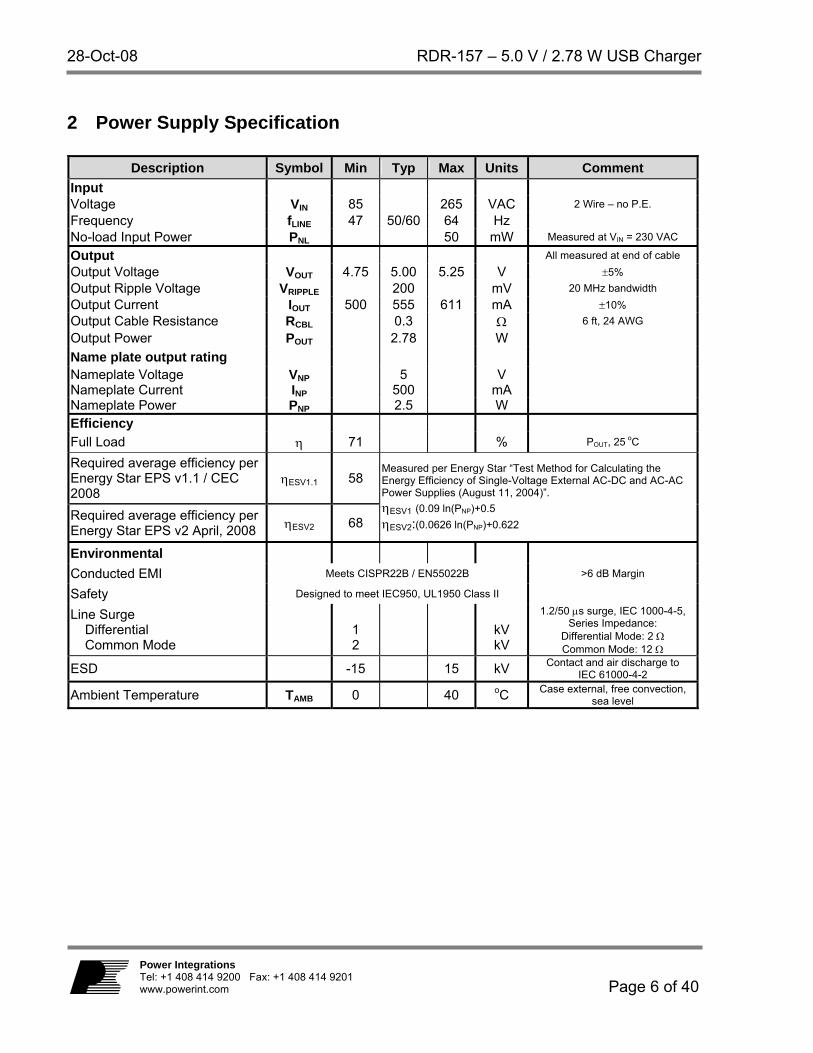
2 Power Supply Specification
Description Symbol Min Typ Max Units Comment Input Voltage VIN 85 265 VAC 2 Wire – no P.E. Frequency fLINE 47 50/60 64 Hz No-load Input Power PNL 50 mW Measured at VIN = 230 VAC
Output All measured at end of cable Output Voltage VOUT 4.75 5.00 5.25 V ±5% Output Ripple Voltage VRIPPLE 200 mV 20 MHz bandwidth Output Current IOUT 500 555 611 mA ±10% Output Cable Resistance RCBL 0.3 Ω 6 ft, 24 AWG
Output Power POUT 2.78 W
Name plate output rating
Nameplate Voltage VNP 5 V Nameplate Current INP 500 mA Nameplate Power PNP 2.5 W
Efficiency
Full Load η 71 % POUT, 25 oC
Required average efficiency per Energy Star EPS v1.1 / CEC 2008
ηESV1.1 58
Required average efficiency per Energy Star EPS v2 April, 2008 ηESV2 68
Measured per Energy Star “Test Method for Calculating the Energy Efficiency of Single-Voltage External AC-DC and AC-AC Power Supplies (August 11, 2004)”. ηESV1 (0.09 ln(PNP)+0.5 ηESV2:(0.0626 ln(PNP)+0.622
Environmental
Conducted EMI Meets CISPR22B / EN55022B >6 dB Margin
Safety Designed to meet IEC950, UL1950 Class II
Line Surge Differential Common Mode
1 2
kV kV
1.2/50 µs surge, IEC 1000-4-5, Series Impedance:
Differential Mode: 2 Ω Common Mode: 12 Ω
ESD -15 15 kV Contact and air discharge to IEC 61000-4-2
Ambient Temperature TAMB 0 40 oC Case external, free convection, sea level
RDR-157 – 5.0 V / 2.78 W USB Charger 28-Oct-08
Page 7 of 40
Power Integrations Tel: +1 408 414 9200 Fax: +1 408 414 9201
www.powerint.com
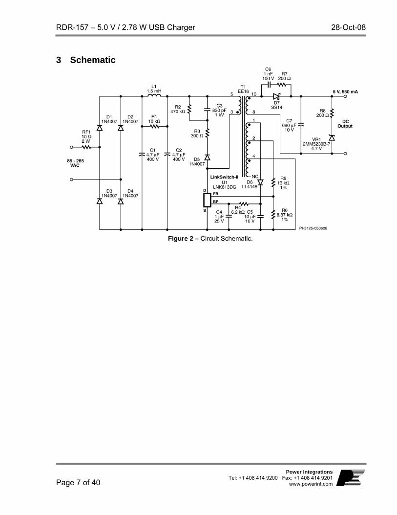
3 Schematic
Figure 2 – Circuit Schematic.
28-Oct-08 RDR-157 – 5.0 V / 2.78 W USB Charger
Page 8 of 40
Power Integrations Tel: +1 408 414 9200 Fax: +1 408 414 9201 www.powerint.com
Circuit Description This circuit uses the LNK613DG in a primary-side regulated flyback power supply configuration.
3.1 Input Filter The AC input power is rectified by diodes D1 through D4. Bulk storage capacitors C1 and C2 filter the rectified AC. Inductor L1 forms a pi (π) filter with C1 and C2 to attenuate conducted differential-mode EMI noise. This configuration, and the use of Power Integrations’ transformer E-shield™ technology, allows this supply to comply with EMI standard EN55022 class B, with good margin, and without a Y capacitor. Fusible resistor RF1 provides protection against catastrophic failure. It should be rated to withstand the instantaneous dissipation when the supply is first connected to AC input (while the input capacitors charge) at VACMAX. This means choosing either an over-sized metal-film or a wire-wound resistor. This design uses a wire-wound resistor for RF1.
3.2 LNK613DG Primary The LNK613DG device (U1) incorporates the power switching device, an oscillator, a CC/CV control engine, startup circuitry, and protection functions into one IC. The integrated 700 V MOSFET allows sufficient voltage margin for universal input AC applications. The device is completely self-powered from the BYPASS pin (BP) and decoupling capacitor C4. Capacitor C4 also selects the output voltage cable-drop compensation amount. For this design standard cable voltage drop compensation was selected by choosing a 1 µF value (to compensate the drop of a 0.3 Ω, 24 AWG USB output cable). The optional bias circuit consisting of D6, C5, and R4 increases efficiency and reduces the no-load input power to less than 40 mW at 265 VAC. The rectified and filtered input voltage is applied to one side of transformer T1’s primary winding. The integrated MOSFET in U1 drives the other side of T1’s primary winding. The leakage inductance drain voltage spike is limited by an RCD-R clamp consisting of D5, R2, R3, and C3. Resistor R3 has a relatively large value to prevent any excessive ringing on the drain voltage waveform, also caused by leakage inductance. When the output voltage is being sampled by the LNK613DG, 2.5 µs after turn off, the sample remains unaffected by such ringing and prevents increased output ripple.
3.3 Output Rectification and Filtering Transformer T1’s secondary is rectified by D7 and filtered by C7. A Schottky barrier-type diode was selected for higher efficiency. Capacitor C7 was selected to have a sufficiently low ESR to meet the output voltage ripple requirement without using an LC post-filter. If it provides lower cost overall, select a smaller value for C7, and follow it with a ferrite bead and another capacitor (100 µF) to provide the necessary filtering to meet the output ripple specification.
RDR-157 – 5.0 V / 2.78 W USB Charger 28-Oct-08
Page 9 of 40
Power Integrations Tel: +1 408 414 9200 Fax: +1 408 414 9201
www.powerint.com
In designs where lower (3% to 4%) average efficiency is acceptable, diode D7 may be replaced by a PN-junction diode to lower cost. Note that R5 and R6 must be re-adjusted to ensure the output voltage stays centered. Capacitor C6 and R7 form a snubber network to both limit the magnitude of the transient voltage spikes that appear across D7 and reduce radiated EMI. Resistor R8 and VR1 form the output pre-load, necessary to prevent the output voltage rising at no-load. The series resistor and Zener diode arrangement vs. a single resistor prevents self discharge when the output is used to charge a battery. In designs where this is not a requirement a single 1 kΩ resistor may be used.
3.4 Output Regulation The LNK613DG regulates the output using ON/OFF control for CV regulation and frequency control for CC regulation. The feedback resistors (R5 and R6) were selected using standard 1% resistor values to center both the nominal output voltage and constant current regulation thresholds.
28-Oct-08 RDR-157 – 5.0 V / 2.78 W USB Charger
Page 10 of 40
Power Integrations Tel: +1 408 414 9200 Fax: +1 408 414 9201 www.powerint.com
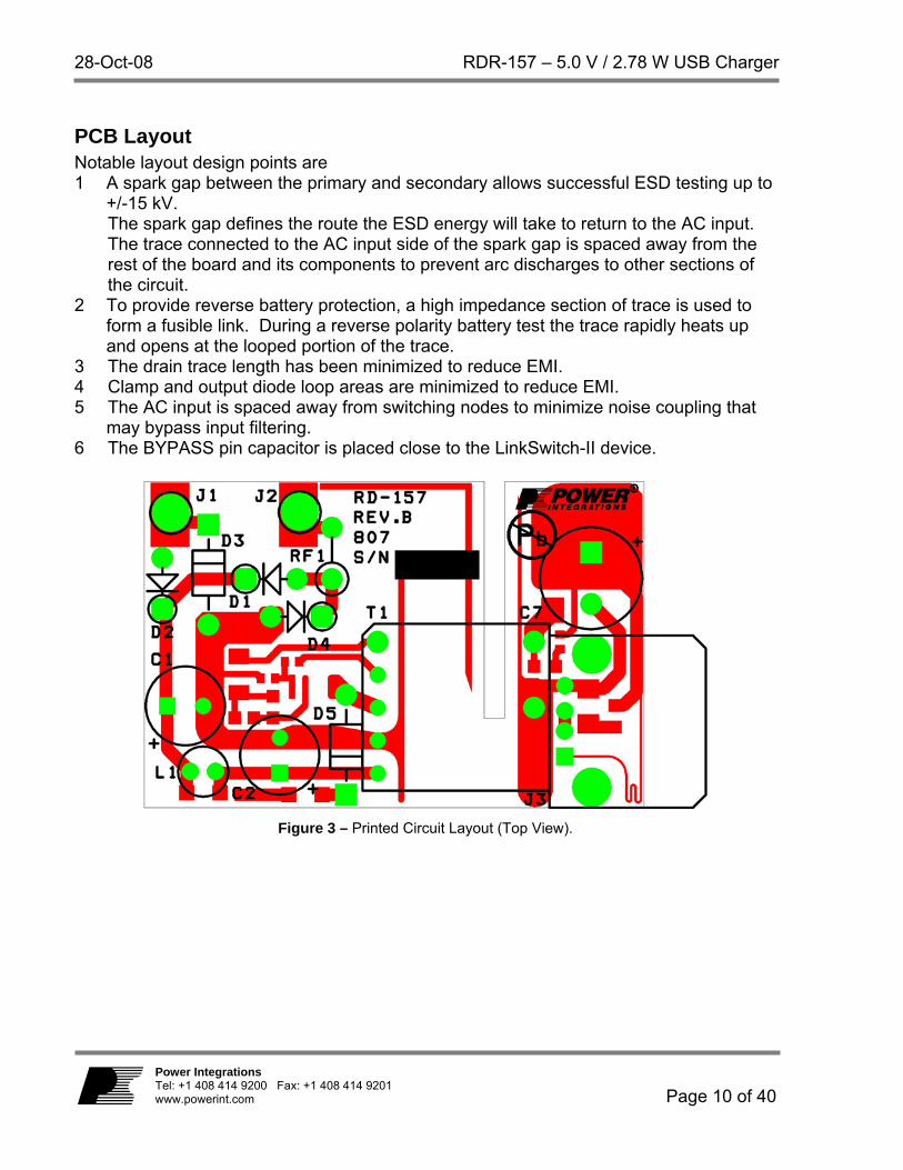
PCB Layout Notable layout design points are 1 A spark gap between the primary and secondary allows successful ESD testing up to
+/-15 kV. The spark gap defines the route the ESD energy will take to return to the AC input. The trace connected to the AC input side of the spark gap is spaced away from the rest of the board and its components to prevent arc discharges to other sections of the circuit.
2 To provide reverse battery protection, a high impedance section of trace is used to form a fusible link. During a reverse polarity battery test the trace rapidly heats up and opens at the looped portion of the trace.
3 The drain trace length has been minimized to reduce EMI. 4 Clamp and output diode loop areas are minimized to reduce EMI. 5 The AC input is spaced away from switching nodes to minimize noise coupling that
may bypass input filtering. 6 The BYPASS pin capacitor is placed close to the LinkSwitch-II device.
Figure 3 – Printed Circuit Layout (Top View).
RDR-157 – 5.0 V / 2.78 W USB Charger 28-Oct-08
Page 11 of 40
Power Integrations Tel: +1 408 414 9200 Fax: +1 408 414 9201
www.powerint.com
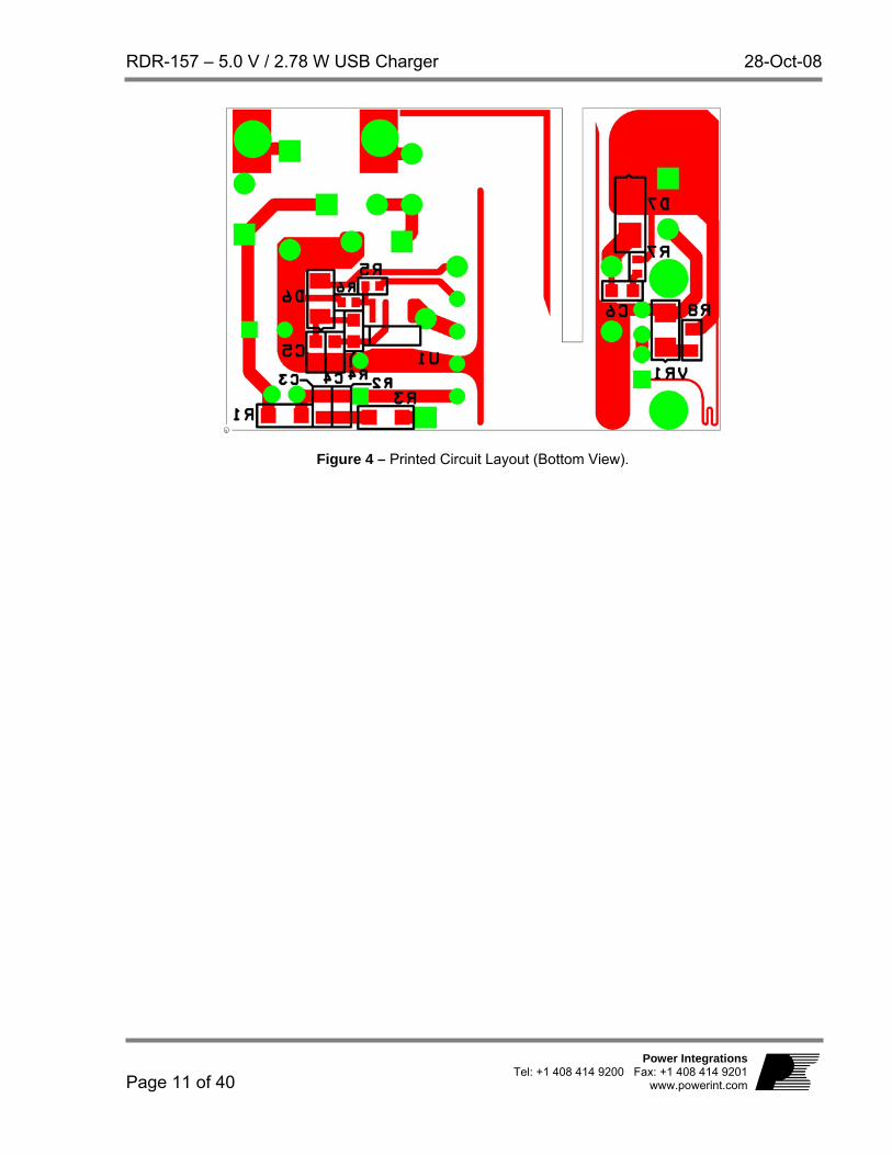
Figure 4 – Printed Circuit Layout (Bottom View).
28-Oct-08 RDR-157 – 5.0 V / 2.78 W USB Charger
Page 12 of 40
Power Integrations Tel: +1 408 414 9200 Fax: +1 408 414 9201 www.powerint.com
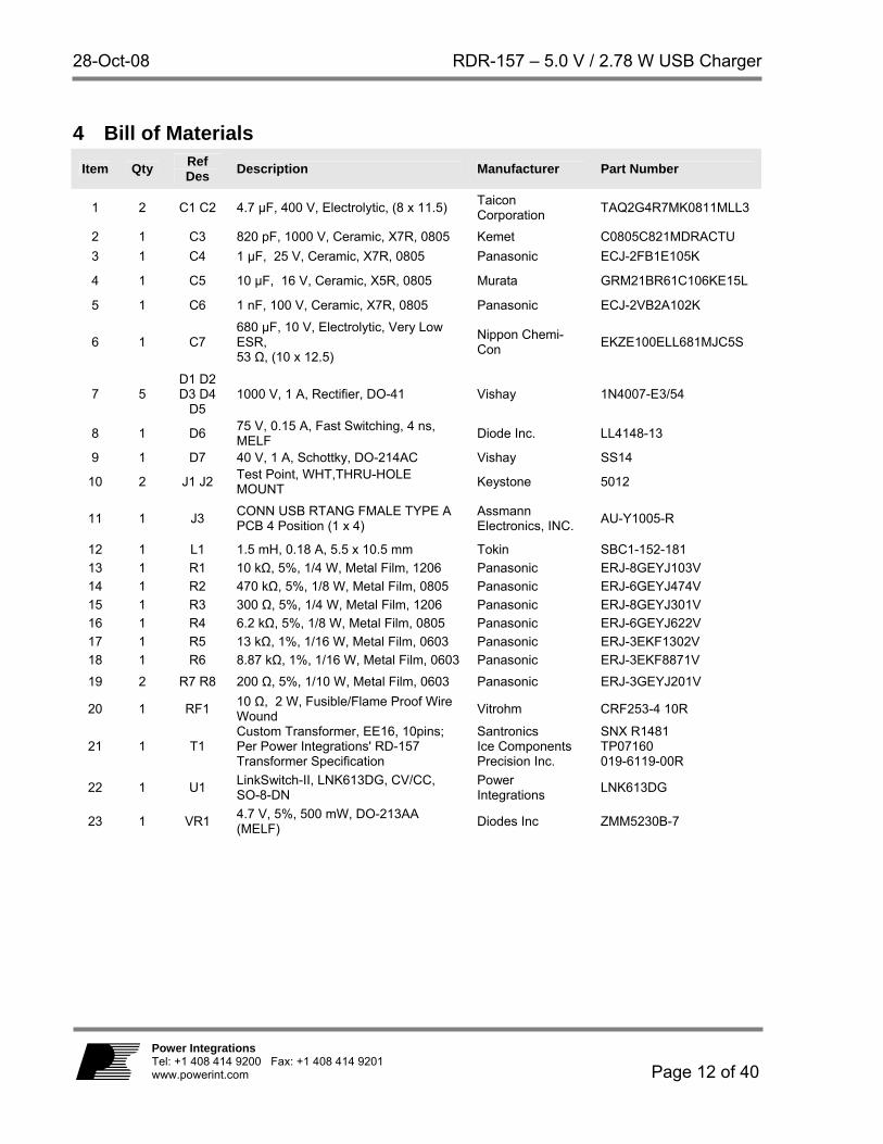
4 Bill of Materials Item Qty Ref
Des Description Manufacturer Part Number
1 2 C1 C2 4.7 µF, 400 V, Electrolytic, (8 x 11.5) Taicon Corporation TAQ2G4R7MK0811MLL3
2 1 C3 820 pF, 1000 V, Ceramic, X7R, 0805 Kemet C0805C821MDRACTU 3 1 C4 1 µF, 25 V, Ceramic, X7R, 0805 Panasonic ECJ-2FB1E105K
4 1 C5 10 µF, 16 V, Ceramic, X5R, 0805 Murata GRM21BR61C106KE15L
5 1 C6 1 nF, 100 V, Ceramic, X7R, 0805 Panasonic ECJ-2VB2A102K
6 1 C7 680 µF, 10 V, Electrolytic, Very Low ESR, 53 Ω, (10 x 12.5)
Nippon Chemi-Con EKZE100ELL681MJC5S
7 5 D1 D2 D3 D4
D5 1000 V, 1 A, Rectifier, DO-41 Vishay 1N4007-E3/54
8 1 D6 75 V, 0.15 A, Fast Switching, 4 ns, MELF Diode Inc. LL4148-13
9 1 D7 40 V, 1 A, Schottky, DO-214AC Vishay SS14
10 2 J1 J2 Test Point, WHT,THRU-HOLE MOUNT Keystone 5012
11 1 J3 CONN USB RTANG FMALE TYPE A PCB 4 Position (1 x 4)
Assmann Electronics, INC. AU-Y1005-R
12 1 L1 1.5 mH, 0.18 A, 5.5 x 10.5 mm Tokin SBC1-152-181 13 1 R1 10 kΩ, 5%, 1/4 W, Metal Film, 1206 Panasonic ERJ-8GEYJ103V 14 1 R2 470 kΩ, 5%, 1/8 W, Metal Film, 0805 Panasonic ERJ-6GEYJ474V 15 1 R3 300 Ω, 5%, 1/4 W, Metal Film, 1206 Panasonic ERJ-8GEYJ301V 16 1 R4 6.2 kΩ, 5%, 1/8 W, Metal Film, 0805 Panasonic ERJ-6GEYJ622V 17 1 R5 13 kΩ, 1%, 1/16 W, Metal Film, 0603 Panasonic ERJ-3EKF1302V 18 1 R6 8.87 kΩ, 1%, 1/16 W, Metal Film, 0603 Panasonic ERJ-3EKF8871V 19 2 R7 R8 200 Ω, 5%, 1/10 W, Metal Film, 0603 Panasonic ERJ-3GEYJ201V
20 1 RF1 10 Ω, 2 W, Fusible/Flame Proof Wire Wound Vitrohm CRF253-4 10R
21 1 T1 Custom Transformer, EE16, 10pins; Per Power Integrations' RD-157 Transformer Specification
Santronics Ice Components Precision Inc.
SNX R1481 TP07160 019-6119-00R
22 1 U1 LinkSwitch-II, LNK613DG, CV/CC, SO-8-DN
Power Integrations LNK613DG
23 1 VR1 4.7 V, 5%, 500 mW, DO-213AA (MELF) Diodes Inc ZMM5230B-7
RDR-157 – 5.0 V / 2.78 W USB Charger 28-Oct-08
Page 13 of 40
Power Integrations Tel: +1 408 414 9200 Fax: +1 408 414 9201
www.powerint.com
5 Transformer Specification
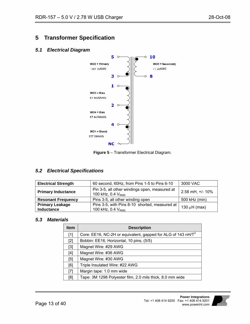
5.1 Electrical Diagram
Figure 5 – Transformer Electrical Diagram.
5.2 Electrical Specifications Electrical Strength 60 second, 60Hz, from Pins 1-5 to Pins 6-10 3000 VAC
Primary Inductance Pin 3-5, all other windings open, measured at 100 kHz, 0.4 VRMS 2.58 mH, +/- 10%
Resonant Frequency Pins 3-5, all other winding open 500 kHz (min) Primary Leakage Inductance
Pins 3-5, with Pins 8-10 shorted, measured at 100 kHz, 0.4 VRMS 130 µH (max)
5.3 Materials Item Description [1] Core: EE16, NC-2H or equivalent, gapped for ALG of 143 nH/T2 [2] Bobbin: EE16, Horizontal, 10 pins, (5/5) [3] Magnet Wire: #29 AWG [4] Magnet Wire: #36 AWG [5] Magnet Wire: #30 AWG [6] Triple Insulated Wire: #22 AWG [7] Margin tape: 1.0 mm wide [8] Tape: 3M 1298 Polyester film, 2.0 mils thick, 8.0 mm wide
28-Oct-08 RDR-157 – 5.0 V / 2.78 W USB Charger
Page 14 of 40
Power Integrations Tel: +1 408 414 9200 Fax: +1 408 414 9201 www.powerint.com
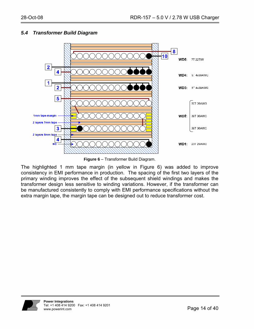
5.4 Transformer Build Diagram
Figure 6 – Transformer Build Diagram.
The highlighted 1 mm tape margin (in yellow in Figure 6) was added to improve consistency in EMI performance in production. The spacing of the first two layers of the primary winding improves the effect of the subsequent shield windings and makes the transformer design less sensitive to winding variations. However, if the transformer can be manufactured consistently to comply with EMI performance specifications without the extra margin tape, the margin tape can be designed out to reduce transformer cost.
RDR-157 – 5.0 V / 2.78 W USB Charger 28-Oct-08
Page 15 of 40
Power Integrations Tel: +1 408 414 9200 Fax: +1 408 414 9201
www.powerint.com
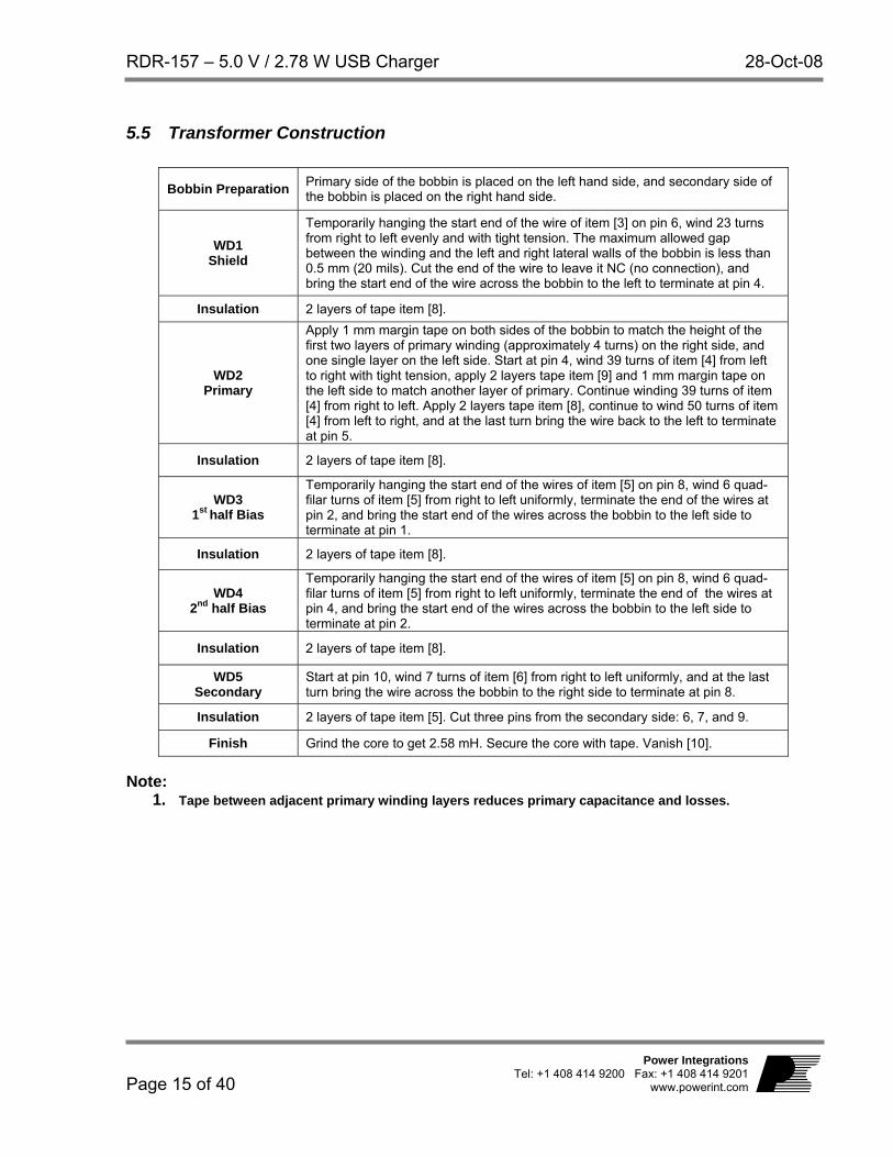
5.5 Transformer Construction
Bobbin Preparation Primary side of the bobbin is placed on the left hand side, and secondary side of the bobbin is placed on the right hand side.
WD1 Shield
Temporarily hanging the start end of the wire of item [3] on pin 6, wind 23 turns from right to left evenly and with tight tension. The maximum allowed gap between the winding and the left and right lateral walls of the bobbin is less than 0.5 mm (20 mils). Cut the end of the wire to leave it NC (no connection), and bring the start end of the wire across the bobbin to the left to terminate at pin 4.
Insulation 2 layers of tape item [8].
WD2 Primary
Apply 1 mm margin tape on both sides of the bobbin to match the height of the first two layers of primary winding (approximately 4 turns) on the right side, and one single layer on the left side. Start at pin 4, wind 39 turns of item [4] from left to right with tight tension, apply 2 layers tape item [9] and 1 mm margin tape on the left side to match another layer of primary. Continue winding 39 turns of item [4] from right to left. Apply 2 layers tape item [8], continue to wind 50 turns of item [4] from left to right, and at the last turn bring the wire back to the left to terminate at pin 5.
Insulation 2 layers of tape item [8].
WD3 1st half Bias
Temporarily hanging the start end of the wires of item [5] on pin 8, wind 6 quad-filar turns of item [5] from right to left uniformly, terminate the end of the wires at pin 2, and bring the start end of the wires across the bobbin to the left side to terminate at pin 1.
Insulation 2 layers of tape item [8].
WD4 2nd half Bias
Temporarily hanging the start end of the wires of item [5] on pin 8, wind 6 quad-filar turns of item [5] from right to left uniformly, terminate the end of the wires at pin 4, and bring the start end of the wires across the bobbin to the left side to terminate at pin 2.
Insulation 2 layers of tape item [8].
WD5 Secondary
Start at pin 10, wind 7 turns of item [6] from right to left uniformly, and at the last turn bring the wire across the bobbin to the right side to terminate at pin 8.
Insulation 2 layers of tape item [5]. Cut three pins from the secondary side: 6, 7, and 9.
Finish Grind the core to get 2.58 mH. Secure the core with tape. Vanish [10]. Note:
1. Tape between adjacent primary winding layers reduces primary capacitance and losses.
28-Oct-08 RDR-157 – 5.0 V / 2.78 W USB Charger
Page 16 of 40
Power Integrations Tel: +1 408 414 9200 Fax: +1 408 414 9201 www.powerint.com
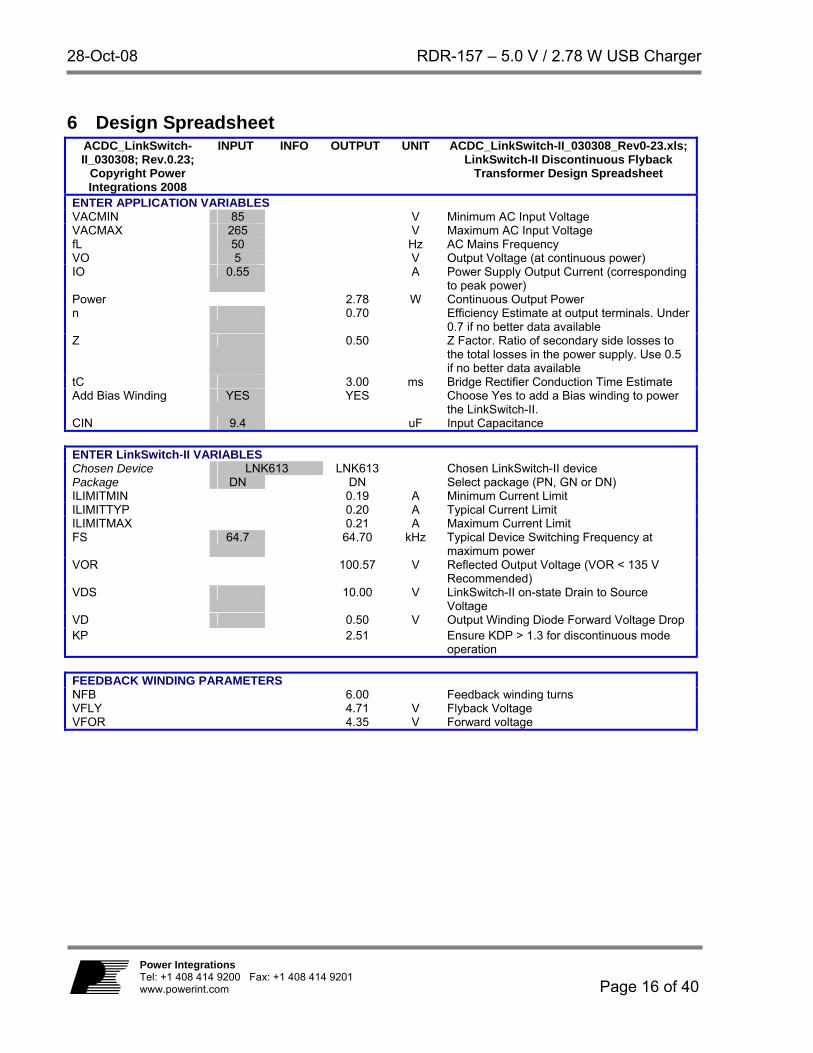
6 Design Spreadsheet ACDC_LinkSwitch-II_030308; Rev.0.23;
Copyright Power Integrations 2008
INPUT INFO OUTPUT UNIT ACDC_LinkSwitch-II_030308_Rev0-23.xls; LinkSwitch-II Discontinuous Flyback
Transformer Design Spreadsheet
ENTER APPLICATION VARIABLES VACMIN 85 V Minimum AC Input Voltage VACMAX 265 V Maximum AC Input Voltage fL 50 Hz AC Mains Frequency VO 5 V Output Voltage (at continuous power) IO 0.55 A Power Supply Output Current (corresponding
to peak power) Power 2.78 W Continuous Output Power n 0.70 Efficiency Estimate at output terminals. Under
0.7 if no better data available Z 0.50 Z Factor. Ratio of secondary side losses to
the total losses in the power supply. Use 0.5 if no better data available
tC 3.00 ms Bridge Rectifier Conduction Time Estimate Add Bias Winding YES YES Choose Yes to add a Bias winding to power
the LinkSwitch-II. CIN 9.4 uF Input Capacitance
ENTER LinkSwitch-II VARIABLES Chosen Device LNK613 LNK613 Chosen LinkSwitch-II device Package DN DN Select package (PN, GN or DN) ILIMITMIN 0.19 A Minimum Current Limit ILIMITTYP 0.20 A Typical Current Limit ILIMITMAX 0.21 A Maximum Current Limit FS 64.7 64.70 kHz Typical Device Switching Frequency at
maximum power VOR 100.57 V Reflected Output Voltage (VOR < 135 V
Recommended) VDS 10.00 V LinkSwitch-II on-state Drain to Source
Voltage VD 0.50 V Output Winding Diode Forward Voltage Drop KP 2.51 Ensure KDP > 1.3 for discontinuous mode
operation
FEEDBACK WINDING PARAMETERS NFB 6.00 Feedback winding turns VFLY 4.71 V Flyback Voltage VFOR 4.35 V Forward voltage
RDR-157 – 5.0 V / 2.78 W USB Charger 28-Oct-08
Page 17 of 40
Power Integrations Tel: +1 408 414 9200 Fax: +1 408 414 9201
www.powerint.com
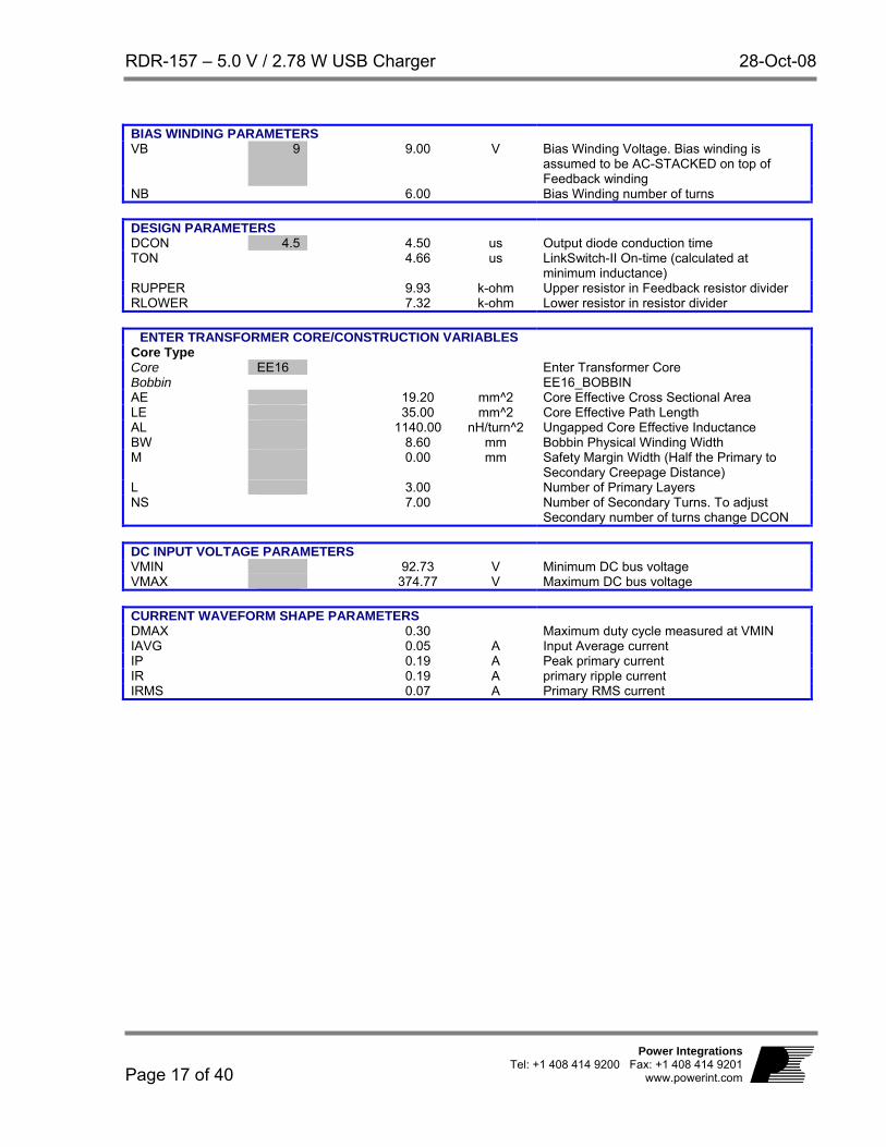
BIAS WINDING PARAMETERS VB 9 9.00 V Bias Winding Voltage. Bias winding is
assumed to be AC-STACKED on top of Feedback winding
NB 6.00 Bias Winding number of turns
DESIGN PARAMETERS DCON 4.5 4.50 us Output diode conduction time TON 4.66 us LinkSwitch-II On-time (calculated at
minimum inductance) RUPPER 9.93 k-ohm Upper resistor in Feedback resistor divider RLOWER 7.32 k-ohm Lower resistor in resistor divider
ENTER TRANSFORMER CORE/CONSTRUCTION VARIABLES
Core Type Core EE16 Enter Transformer Core Bobbin EE16_BOBBIN AE 19.20 mm^2 Core Effective Cross Sectional Area LE 35.00 mm^2 Core Effective Path Length AL 1140.00 nH/turn^2 Ungapped Core Effective Inductance BW 8.60 mm Bobbin Physical Winding Width M 0.00 mm Safety Margin Width (Half the Primary to
Secondary Creepage Distance) L 3.00 Number of Primary Layers NS 7.00 Number of Secondary Turns. To adjust
Secondary number of turns change DCON
DC INPUT VOLTAGE PARAMETERS VMIN 92.73 V Minimum DC bus voltage VMAX 374.77 V Maximum DC bus voltage
CURRENT WAVEFORM SHAPE PARAMETERS DMAX 0.30 Maximum duty cycle measured at VMIN IAVG 0.05 A Input Average current IP 0.19 A Peak primary current IR 0.19 A primary ripple current IRMS 0.07 A Primary RMS current
28-Oct-08 RDR-157 – 5.0 V / 2.78 W USB Charger
Page 18 of 40
Power Integrations Tel: +1 408 414 9200 Fax: +1 408 414 9201 www.powerint.com
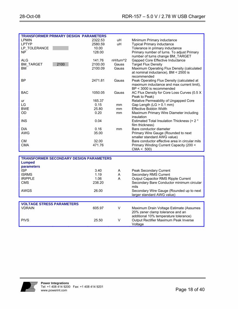
TRANSFORMER PRIMARY DESIGN PARAMETERS LPMIN 2322.53 uH Minimum Primary inductance LPTYP 2580.59 uH Typical Primary inductance LP_TOLERANCE 10.00 Tolerance in primary inductance NP 128.00 Primary number of turns. To adjust Primary
number of turns change BM_TARGET ALG 141.76 nH/turn^2 Gapped Core Effective Inductance BM_TARGET 2100 2100.00 Gauss Target Flux Density BM 2100.09 Gauss Maximum Operating Flux Density (calculated
at nominal inductance), BM < 2500 is recommended
BP 2471.81 Gauss Peak Operating Flux Density (calculated at maximum inductance and max current limit), BP < 3000 is recommended
BAC 1050.05 Gauss AC Flux Density for Core Loss Curves (0.5 X Peak to Peak)
ur 165.37 Relative Permeability of Ungapped Core LG 0.15 mm Gap Length (LG > 0.1 mm) BWE 25.80 mm Effective Bobbin Width OD 0.20 mm Maximum Primary Wire Diameter including
insulation INS 0.04 Estimated Total Insulation Thickness (= 2 *
film thickness) DIA 0.16 mm Bare conductor diameter AWG 35.00 Primary Wire Gauge (Rounded to next
smaller standard AWG value) CM 32.00 Bare conductor effective area in circular mils CMA 471.76 Primary Winding Current Capacity (200 <
CMA < 500)
TRANSFORMER SECONDARY DESIGN PARAMETERS Lumped parameters
ISP 3.40 A Peak Secondary Current ISRMS 1.19 A Secondary RMS Current IRIPPLE 1.06 A Output Capacitor RMS Ripple Current CMS 238.20 Secondary Bare Conductor minimum circular
mils AWGS 26.00 Secondary Wire Gauge (Rounded up to next
larger standard AWG value)
VOLTAGE STRESS PARAMETERS VDRAIN 605.97 V Maximum Drain Voltage Estimate (Assumes
20% zener clamp tolerance and an additional 10% temperature tolerance)
PIVS 25.50 V Output Rectifier Maximum Peak Inverse Voltage
RDR-157 – 5.0 V / 2.78 W USB Charger 28-Oct-08
Page 19 of 40
Power Integrations Tel: +1 408 414 9200 Fax: +1 408 414 9201
www.powerint.com
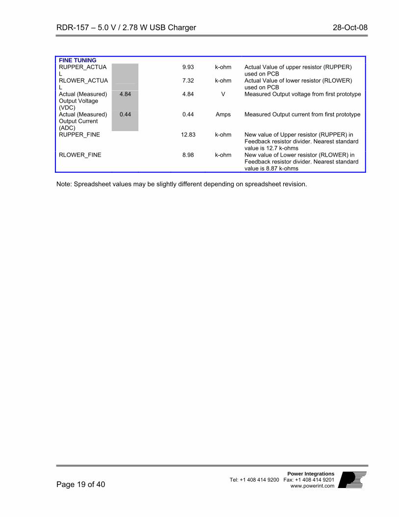
FINE TUNING RUPPER_ACTUAL
9.93 k-ohm Actual Value of upper resistor (RUPPER) used on PCB
RLOWER_ACTUAL
7.32 k-ohm Actual Value of lower resistor (RLOWER) used on PCB
Actual (Measured) Output Voltage (VDC)
4.84 4.84 V Measured Output voltage from first prototype
Actual (Measured) Output Current (ADC)
0.44 0.44 Amps Measured Output current from first prototype
RUPPER_FINE 12.83 k-ohm New value of Upper resistor (RUPPER) in Feedback resistor divider. Nearest standard value is 12.7 k-ohms
RLOWER_FINE 8.98 k-ohm New value of Lower resistor (RLOWER) in Feedback resistor divider. Nearest standard value is 8.87 k-ohms
Note: Spreadsheet values may be slightly different depending on spreadsheet revision.
28-Oct-08 RDR-157 – 5.0 V / 2.78 W USB Charger
Page 20 of 40
Power Integrations Tel: +1 408 414 9200 Fax: +1 408 414 9201 www.powerint.com
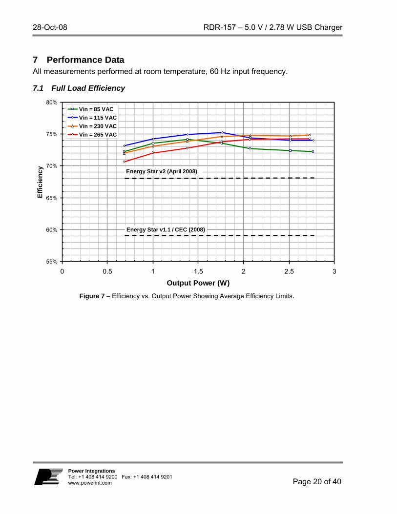
7 Performance Data All measurements performed at room temperature, 60 Hz input frequency.
7.1 Full Load Efficiency
55%
60%
65%
70%
75%
80%
0 0.5 1 1.5 2 2.5 3
Output Power (W)
Effic
ienc
y
Vin = 85 VACVin = 115 VACVin = 230 VACVin = 265 VAC
Energy Star v1.1 / CEC (2008)
Energy Star v2 (April 2008)
Figure 7 – Efficiency vs. Output Power Showing Average Efficiency Limits.
RDR-157 – 5.0 V / 2.78 W USB Charger 28-Oct-08
Page 21 of 40
Power Integrations Tel: +1 408 414 9200 Fax: +1 408 414 9201
www.powerint.com
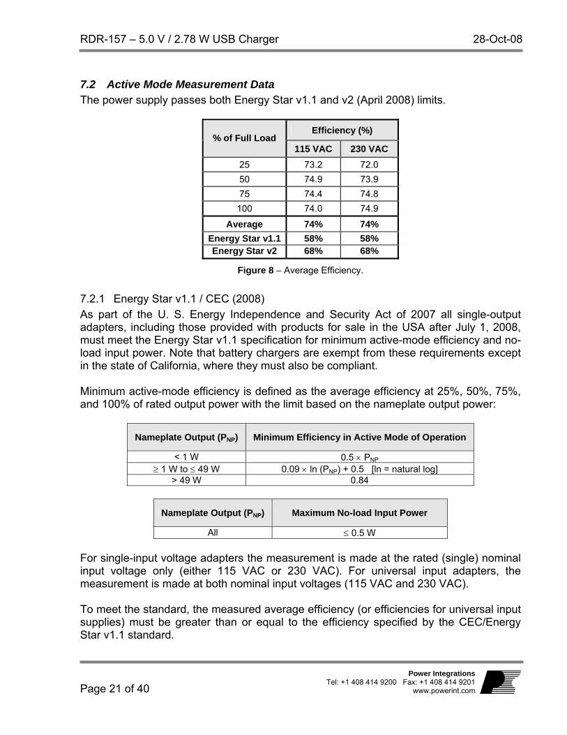
7.2 Active Mode Measurement Data The power supply passes both Energy Star v1.1 and v2 (April 2008) limits.
Efficiency (%) % of Full Load
115 VAC 230 VAC
25 73.2 72.0 50 74.9 73.9 75 74.4 74.8
100 74.0 74.9
Average 74% 74% Energy Star v1.1 58% 58% Energy Star v2 68% 68%
Figure 8 – Average Efficiency.
7.2.1 Energy Star v1.1 / CEC (2008) As part of the U. S. Energy Independence and Security Act of 2007 all single-output adapters, including those provided with products for sale in the USA after July 1, 2008, must meet the Energy Star v1.1 specification for minimum active-mode efficiency and no-load input power. Note that battery chargers are exempt from these requirements except in the state of California, where they must also be compliant. Minimum active-mode efficiency is defined as the average efficiency at 25%, 50%, 75%, and 100% of rated output power with the limit based on the nameplate output power:
Nameplate Output (PNP) Minimum Efficiency in Active Mode of Operation
< 1 W 0.5 × PNP ≥ 1 W to ≤ 49 W 0.09 × ln (PNP) + 0.5 [ln = natural log]
> 49 W 0.84
Nameplate Output (PNP) Maximum No-load Input Power
All ≤ 0.5 W For single-input voltage adapters the measurement is made at the rated (single) nominal input voltage only (either 115 VAC or 230 VAC). For universal input adapters, the measurement is made at both nominal input voltages (115 VAC and 230 VAC). To meet the standard, the measured average efficiency (or efficiencies for universal input supplies) must be greater than or equal to the efficiency specified by the CEC/Energy Star v1.1 standard.
28-Oct-08 RDR-157 – 5.0 V / 2.78 W USB Charger
Page 22 of 40
Power Integrations Tel: +1 408 414 9200 Fax: +1 408 414 9201 www.powerint.com
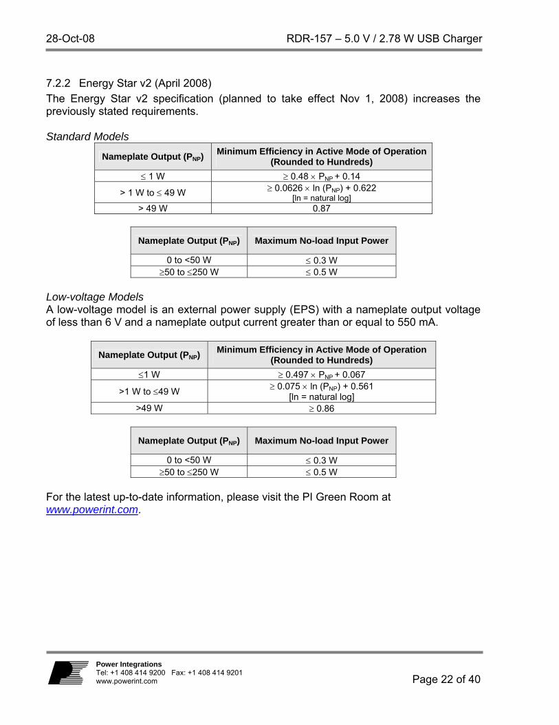
7.2.2 Energy Star v2 (April 2008) The Energy Star v2 specification (planned to take effect Nov 1, 2008) increases the previously stated requirements. Standard Models
Nameplate Output (PNP) Minimum Efficiency in Active Mode of Operation (Rounded to Hundreds)
≤ 1 W ≥ 0.48 × PNP + 0.14
> 1 W to ≤ 49 W ≥ 0.0626 × ln (PNP) + 0.622 [ln = natural log]
> 49 W 0.87
Nameplate Output (PNP) Maximum No-load Input Power
0 to <50 W ≤ 0.3 W ≥50 to ≤250 W ≤ 0.5 W
Low-voltage Models A low-voltage model is an external power supply (EPS) with a nameplate output voltage of less than 6 V and a nameplate output current greater than or equal to 550 mA.
Nameplate Output (PNP) Minimum Efficiency in Active Mode of Operation (Rounded to Hundreds)
≤1 W ≥ 0.497 × PNP + 0.067
>1 W to ≤49 W ≥ 0.075 × ln (PNP) + 0.561 [ln = natural log]
>49 W ≥ 0.86
Nameplate Output (PNP) Maximum No-load Input Power
0 to <50 W ≤ 0.3 W ≥50 to ≤250 W ≤ 0.5 W
For the latest up-to-date information, please visit the PI Green Room at www.powerint.com.
RDR-157 – 5.0 V / 2.78 W USB Charger 28-Oct-08
Page 23 of 40
Power Integrations Tel: +1 408 414 9200 Fax: +1 408 414 9201
www.powerint.com
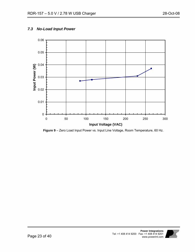
7.3 No-Load Input Power
0
0.01
0.02
0.03
0.04
0.05
0.06
0 50 100 150 200 250 300
Input Voltage (VAC)
Inpu
t Pow
er (W
)
Figure 9 – Zero Load Input Power vs. Input Line Voltage, Room Temperature, 60 Hz.
28-Oct-08 RDR-157 – 5.0 V / 2.78 W USB Charger
Page 24 of 40
Power Integrations Tel: +1 408 414 9200 Fax: +1 408 414 9201 www.powerint.com
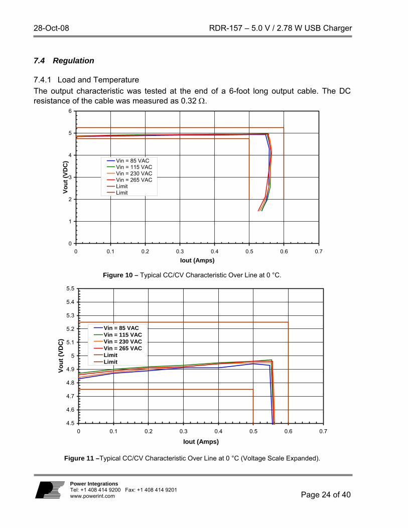
7.4 Regulation
7.4.1 Load and Temperature The output characteristic was tested at the end of a 6-foot long output cable. The DC resistance of the cable was measured as 0.32 Ω.
0
1
2
3
4
5
6
0 0.1 0.2 0.3 0.4 0.5 0.6 0.7
Iout (Amps)
Vout
(VD
C) Vin = 85 VAC
Vin = 115 VACVin = 230 VACVin = 265 VACLimitLimit
Figure 10 – Typical CC/CV Characteristic Over Line at 0 °C.
4.5
4.6
4.7
4.8
4.9
5
5.1
5.2
5.3
5.4
5.5
0 0.1 0.2 0.3 0.4 0.5 0.6 0.7
Iout (Amps)
Vout
(VD
C)
Vin = 85 VACVin = 115 VACVin = 230 VACVin = 265 VACLimitLimit
Figure 11 –Typical CC/CV Characteristic Over Line at 0 °C (Voltage Scale Expanded).
RDR-157 – 5.0 V / 2.78 W USB Charger 28-Oct-08
Page 25 of 40
Power Integrations Tel: +1 408 414 9200 Fax: +1 408 414 9201
www.powerint.com
0
1
2
3
4
5
6
0 0.1 0.2 0.3 0.4 0.5 0.6 0.7
Iout (Amps)
Vout
(VD
C) Vin = 85 VAC
Vin = 115 VACVin = 230 VACVin = 265 VACLimitLimit
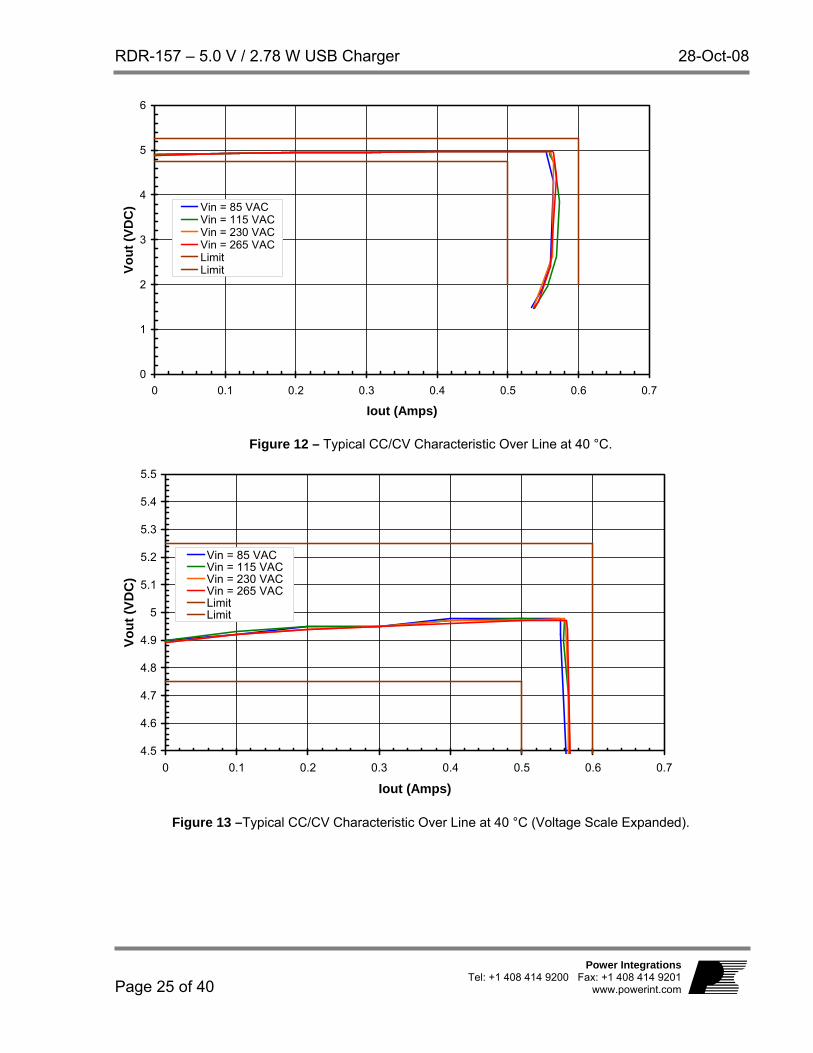
Figure 12 – Typical CC/CV Characteristic Over Line at 40 °C.
4.5
4.6
4.7
4.8
4.9
5
5.1
5.2
5.3
5.4
5.5
0 0.1 0.2 0.3 0.4 0.5 0.6 0.7
Iout (Amps)
Vout
(VD
C)
Vin = 85 VACVin = 115 VACVin = 230 VACVin = 265 VACLimitLimit
Figure 13 –Typical CC/CV Characteristic Over Line at 40 °C (Voltage Scale Expanded).
28-Oct-08 RDR-157 – 5.0 V / 2.78 W USB Charger
Page 26 of 40
Power Integrations Tel: +1 408 414 9200 Fax: +1 408 414 9201 www.powerint.com
0
1
2
3
4
5
6
0 0.1 0.2 0.3 0.4 0.5 0.6 0.7
Iout (Amps)
Vout
(VD
C) Vin = 85 VAC
Vin = 115 VACVin = 230 VACVin = 265 VACLimitLimit
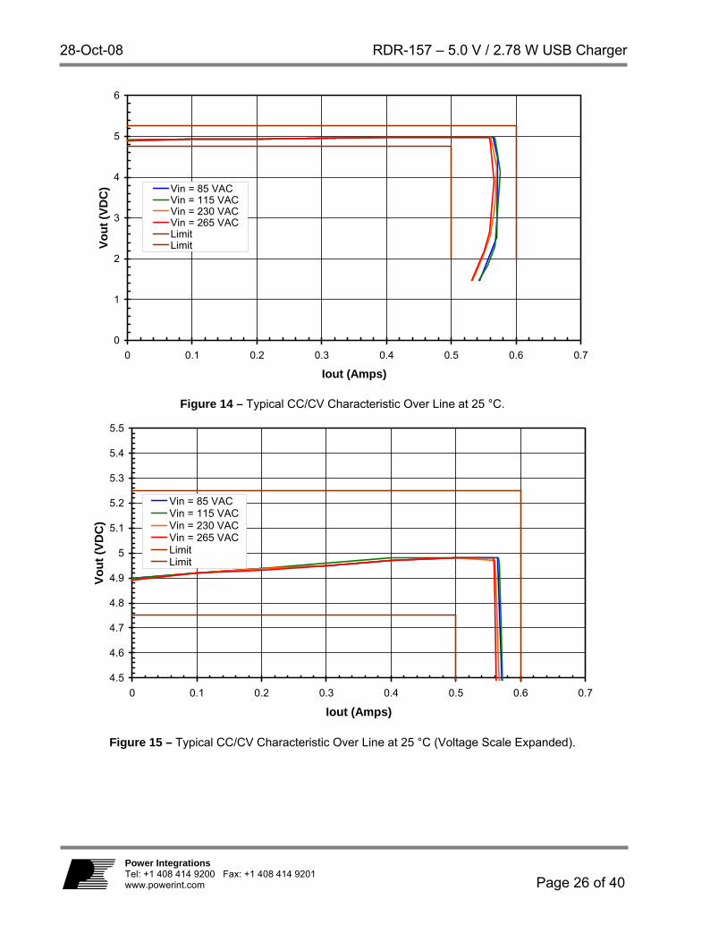
Figure 14 – Typical CC/CV Characteristic Over Line at 25 °C.
4.5
4.6
4.7
4.8
4.9
5
5.1
5.2
5.3
5.4
5.5
0 0.1 0.2 0.3 0.4 0.5 0.6 0.7
Iout (Amps)
Vout
(VD
C)
Vin = 85 VACVin = 115 VACVin = 230 VACVin = 265 VACLimitLimit
Figure 15 – Typical CC/CV Characteristic Over Line at 25 °C (Voltage Scale Expanded).
RDR-157 – 5.0 V / 2.78 W USB Charger 28-Oct-08
Page 27 of 40
Power Integrations Tel: +1 408 414 9200 Fax: +1 408 414 9201
www.powerint.com
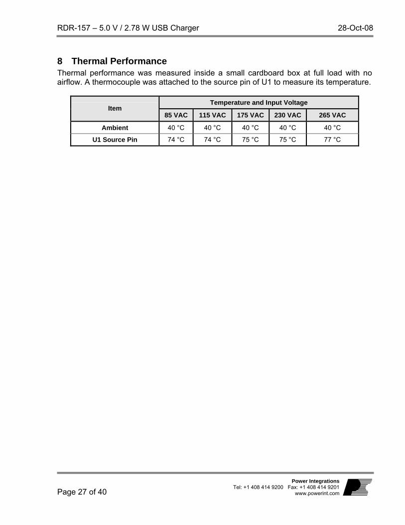
8 Thermal Performance Thermal performance was measured inside a small cardboard box at full load with no airflow. A thermocouple was attached to the source pin of U1 to measure its temperature.
Temperature and Input Voltage Item
85 VAC 115 VAC 175 VAC 230 VAC 265 VAC
Ambient 40 °C 40 °C 40 °C 40 °C 40 °C
U1 Source Pin 74 °C 74 °C 75 °C 75 °C 77 °C
28-Oct-08 RDR-157 – 5.0 V / 2.78 W USB Charger
Page 28 of 40
Power Integrations Tel: +1 408 414 9200 Fax: +1 408 414 9201 www.powerint.com
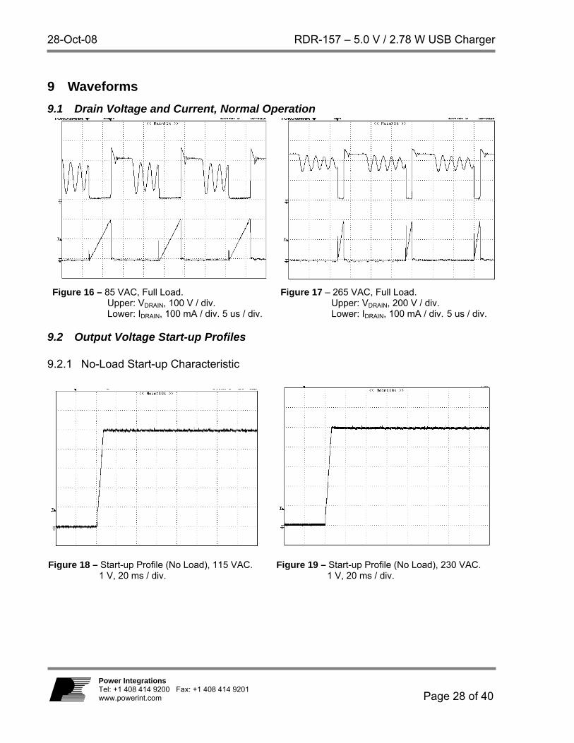
9 Waveforms 9.1 Drain Voltage and Current, Normal Operation
Figure 16 – 85 VAC, Full Load.
Upper: VDRAIN, 100 V / div. Lower: IDRAIN, 100 mA / div. 5 us / div.
Figure 17 – 265 VAC, Full Load. Upper: VDRAIN, 200 V / div. Lower: IDRAIN, 100 mA / div. 5 us / div.
9.2 Output Voltage Start-up Profiles
9.2.1 No-Load Start-up Characteristic
Figure 18 – Start-up Profile (No Load), 115 VAC. 1 V, 20 ms / div.
Figure 19 – Start-up Profile (No Load), 230 VAC. 1 V, 20 ms / div.
RDR-157 – 5.0 V / 2.78 W USB Charger 28-Oct-08
Page 29 of 40
Power Integrations Tel: +1 408 414 9200 Fax: +1 408 414 9201
www.powerint.com
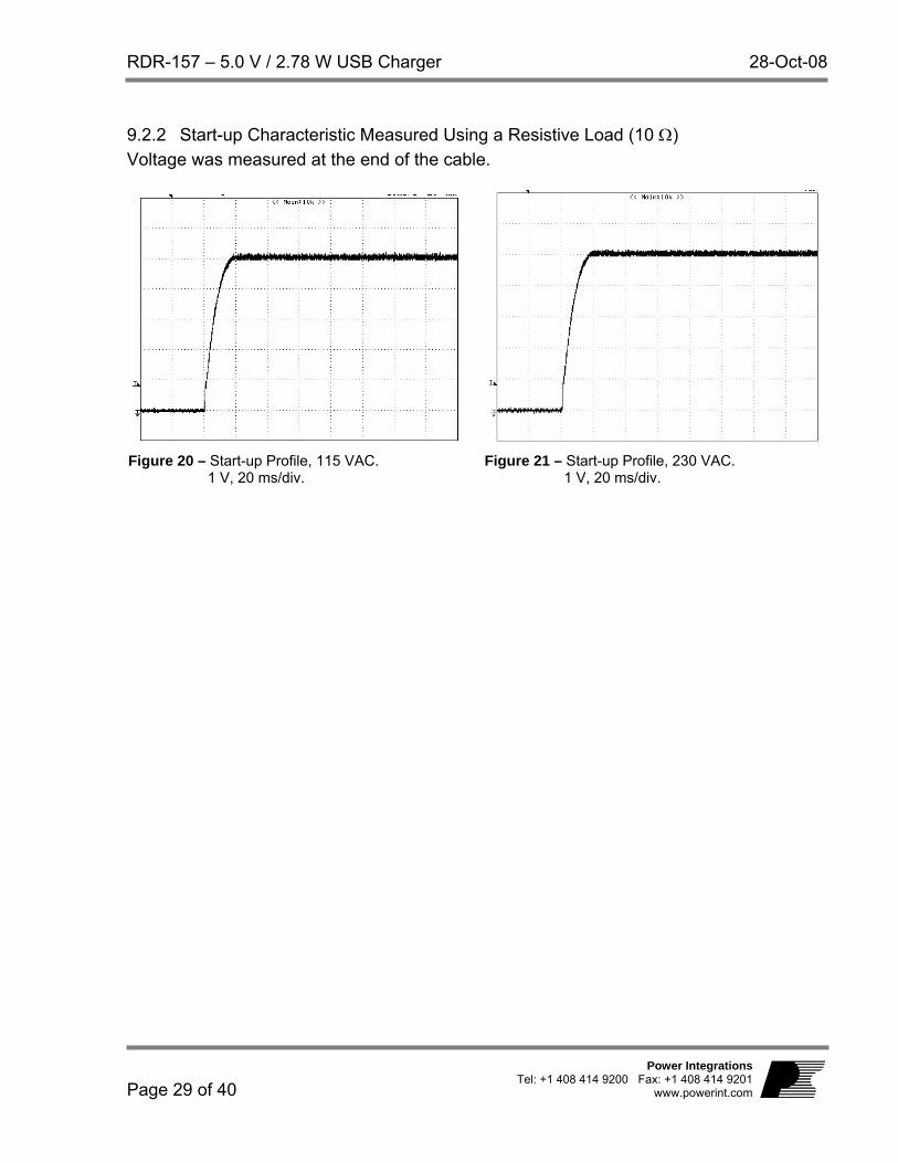
9.2.2 Start-up Characteristic Measured Using a Resistive Load (10 Ω) Voltage was measured at the end of the cable.
Figure 20 – Start-up Profile, 115 VAC.
1 V, 20 ms/div. Figure 21 – Start-up Profile, 230 VAC.
1 V, 20 ms/div.
28-Oct-08 RDR-157 – 5.0 V / 2.78 W USB Charger
Page 30 of 40
Power Integrations Tel: +1 408 414 9200 Fax: +1 408 414 9201 www.powerint.com
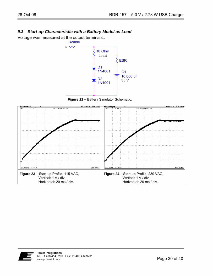
9.3 Start-up Characteristic with a Battery Model as Load Voltage was measured at the output terminals..
C110,000 uF35 V
D11N4001
D21N4001
ESR
10 Ohm
Rcable
Load
Figure 22 – Battery Simulator Schematic.
Figure 23 – Start-up Profile, 115 VAC, Vertical: 1 V / div. Horizontal: 20 ms / div.
Figure 24 – Start-up Profile, 230 VAC, Vertical: 1 V / div. Horizontal: 20 ms / div.
RDR-157 – 5.0 V / 2.78 W USB Charger 28-Oct-08
Page 31 of 40
Power Integrations Tel: +1 408 414 9200 Fax: +1 408 414 9201
www.powerint.com
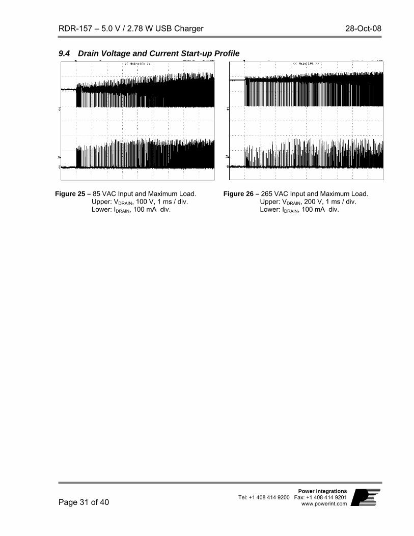
9.4 Drain Voltage and Current Start-up Profile
Figure 25 – 85 VAC Input and Maximum Load. Upper: VDRAIN, 100 V, 1 ms / div. Lower: IDRAIN, 100 mA div.
Figure 26 – 265 VAC Input and Maximum Load. Upper: VDRAIN, 200 V, 1 ms / div. Lower: IDRAIN, 100 mA div.
28-Oct-08 RDR-157 – 5.0 V / 2.78 W USB Charger
Page 32 of 40
Power Integrations Tel: +1 408 414 9200 Fax: +1 408 414 9201 www.powerint.com
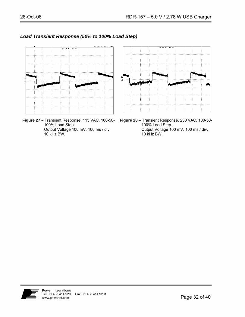
Load Transient Response (50% to 100% Load Step)
Figure 27 – Transient Response, 115 VAC, 100-50-100% Load Step. Output Voltage 100 mV, 100 ms / div. 10 kHz BW.
Figure 28 – Transient Response, 230 VAC, 100-50-100% Load Step. Output Voltage 100 mV, 100 ms / div. 10 kHz BW.
RDR-157 – 5.0 V / 2.78 W USB Charger 28-Oct-08
Page 33 of 40
Power Integrations Tel: +1 408 414 9200 Fax: +1 408 414 9201
www.powerint.com
9.5 Output Ripple Measurements
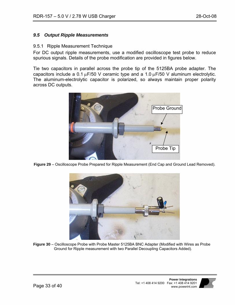
9.5.1 Ripple Measurement Technique For DC output ripple measurements, use a modified oscilloscope test probe to reduce spurious signals. Details of the probe modification are provided in figures below. Tie two capacitors in parallel across the probe tip of the 5125BA probe adapter. The capacitors include a 0.1 µF/50 V ceramic type and a 1.0 µF/50 V aluminum electrolytic. The aluminum-electrolytic capacitor is polarized, so always maintain proper polarity across DC outputs.
Figure 29 – Oscilloscope Probe Prepared for Ripple Measurement (End Cap and Ground Lead Removed).
Figure 30 – Oscilloscope Probe with Probe Master 5125BA BNC Adapter (Modified with Wires as Probe
Ground for Ripple measurement with two Parallel Decoupling Capacitors Added).
Probe Ground
Probe Tip
28-Oct-08 RDR-157 – 5.0 V / 2.78 W USB Charger
Page 34 of 40
Power Integrations Tel: +1 408 414 9200 Fax: +1 408 414 9201 www.powerint.com
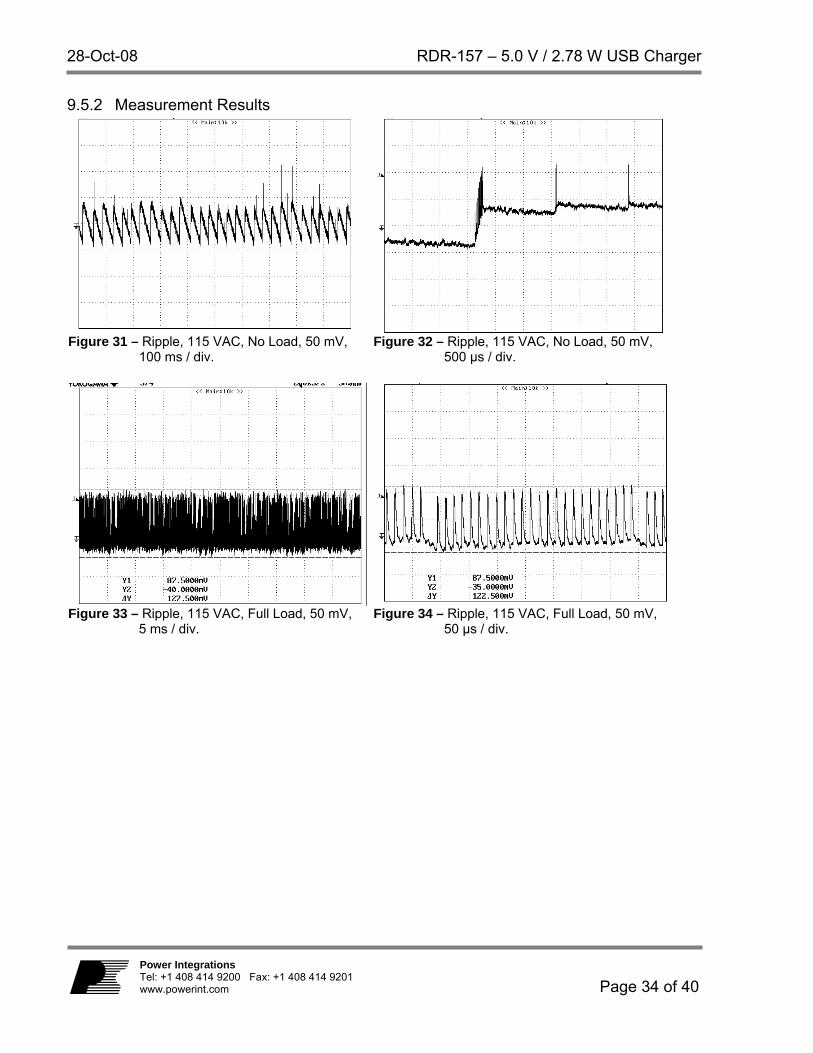
9.5.2 Measurement Results
Figure 31 – Ripple, 115 VAC, No Load, 50 mV,
100 ms / div. Figure 32 – Ripple, 115 VAC, No Load, 50 mV,
500 µs / div.
Figure 33 – Ripple, 115 VAC, Full Load, 50 mV,
5 ms / div. Figure 34 – Ripple, 115 VAC, Full Load, 50 mV,
50 µs / div.
RDR-157 – 5.0 V / 2.78 W USB Charger 28-Oct-08
Page 35 of 40
Power Integrations Tel: +1 408 414 9200 Fax: +1 408 414 9201
www.powerint.com
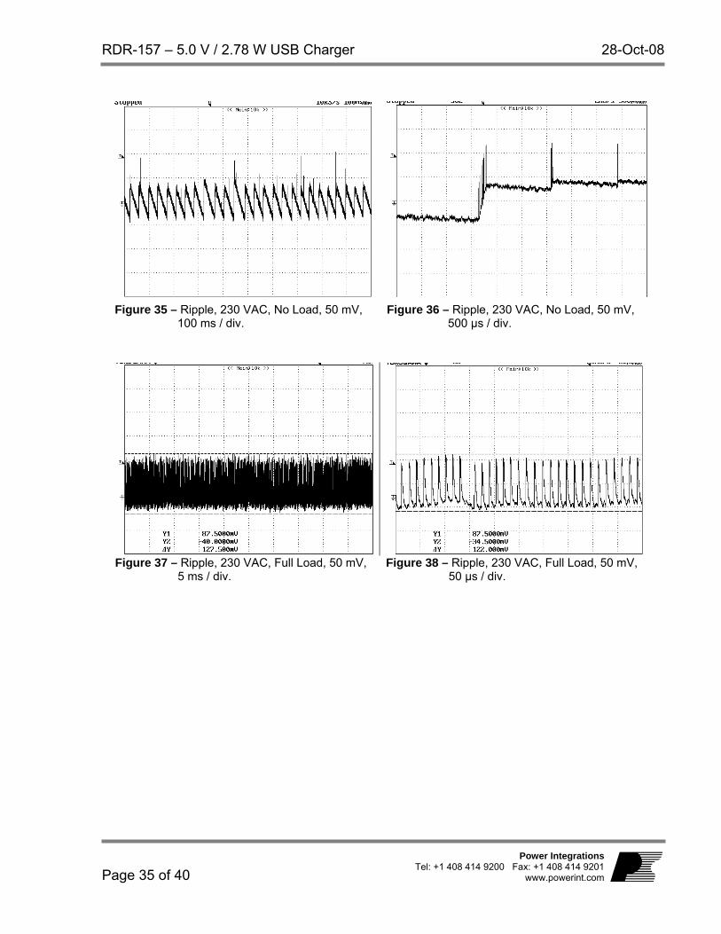
Figure 35 – Ripple, 230 VAC, No Load, 50 mV, 100 ms / div.
Figure 36 – Ripple, 230 VAC, No Load, 50 mV, 500 µs / div.
Figure 37 – Ripple, 230 VAC, Full Load, 50 mV,
5 ms / div. Figure 38 – Ripple, 230 VAC, Full Load, 50 mV,
50 µs / div.
28-Oct-08 RDR-157 – 5.0 V / 2.78 W USB Charger
Page 36 of 40
Power Integrations Tel: +1 408 414 9200 Fax: +1 408 414 9201 www.powerint.com
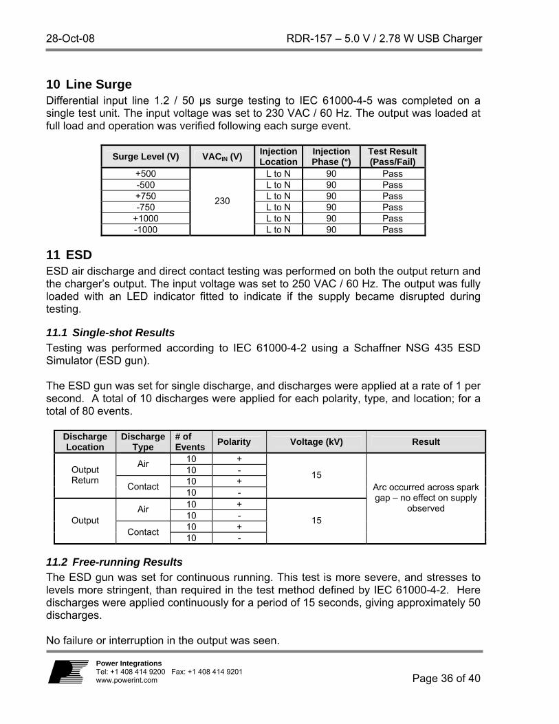
10 Line Surge Differential input line 1.2 / 50 µs surge testing to IEC 61000-4-5 was completed on a single test unit. The input voltage was set to 230 VAC / 60 Hz. The output was loaded at full load and operation was verified following each surge event.
Surge Level (V) VACIN (V) Injection Location
Injection Phase (°)
Test Result (Pass/Fail)
+500 L to N 90 Pass -500 L to N 90 Pass +750 L to N 90 Pass -750 L to N 90 Pass
+1000 L to N 90 Pass -1000
230
L to N 90 Pass
11 ESD ESD air discharge and direct contact testing was performed on both the output return and the charger’s output. The input voltage was set to 250 VAC / 60 Hz. The output was fully loaded with an LED indicator fitted to indicate if the supply became disrupted during testing.
11.1 Single-shot Results Testing was performed according to IEC 61000-4-2 using a Schaffner NSG 435 ESD Simulator (ESD gun). The ESD gun was set for single discharge, and discharges were applied at a rate of 1 per second. A total of 10 discharges were applied for each polarity, type, and location; for a total of 80 events.
Discharge Location
Discharge Type
# of Events Polarity Voltage (kV) Result
10 + Air 10 - 10 +
Output Return
Contact 10 -
15
10 + Air 10 - 10 +
Output Contact 10 -
15
Arc occurred across spark gap – no effect on supply
observed
11.2 Free-running Results The ESD gun was set for continuous running. This test is more severe, and stresses to levels more stringent, than required in the test method defined by IEC 61000-4-2. Here discharges were applied continuously for a period of 15 seconds, giving approximately 50 discharges. No failure or interruption in the output was seen.
RDR-157 – 5.0 V / 2.78 W USB Charger 28-Oct-08
Page 37 of 40
Power Integrations Tel: +1 408 414 9200 Fax: +1 408 414 9201
www.powerint.com
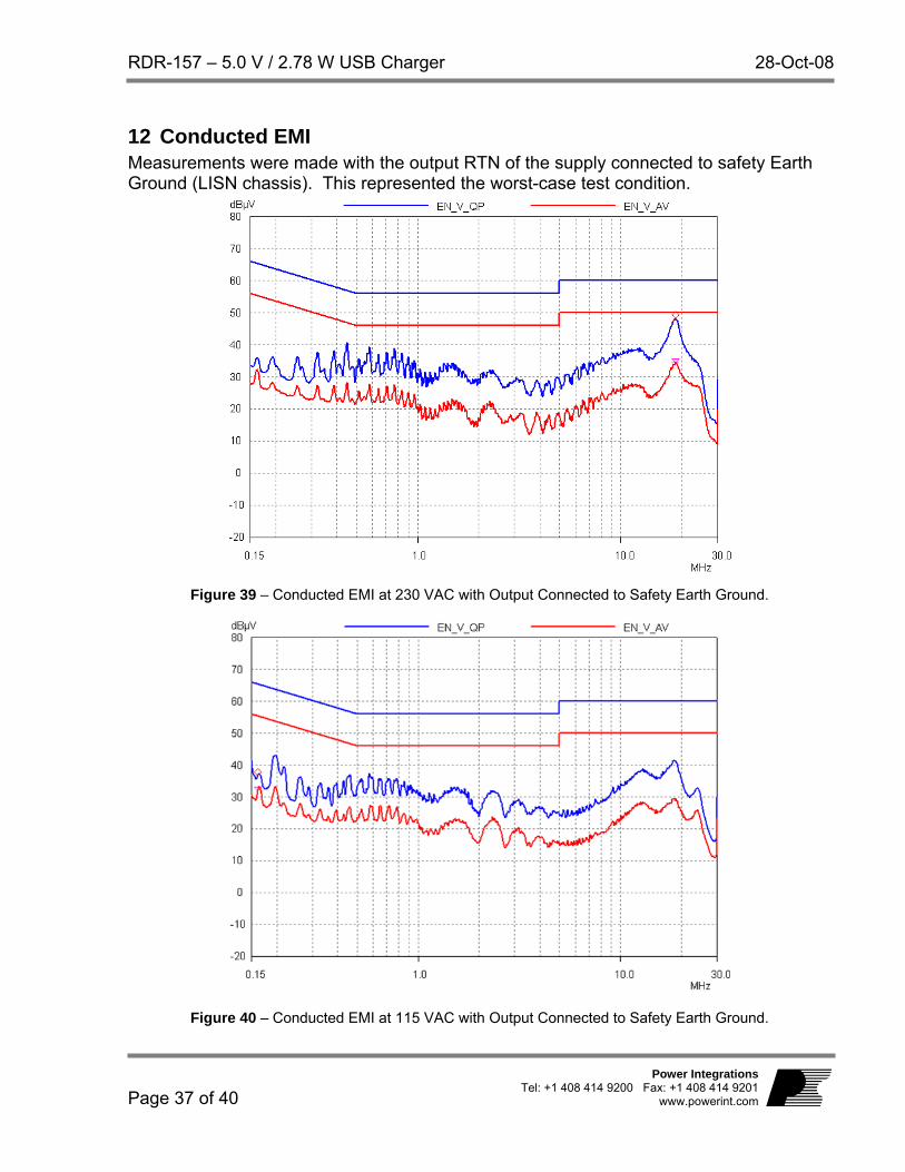
12 Conducted EMI Measurements were made with the output RTN of the supply connected to safety Earth Ground (LISN chassis). This represented the worst-case test condition.
Figure 39 – Conducted EMI at 230 VAC with Output Connected to Safety Earth Ground.
Figure 40 – Conducted EMI at 115 VAC with Output Connected to Safety Earth Ground.
28-Oct-08 RDR-157 – 5.0 V / 2.78 W USB Charger
Page 38 of 40
Power Integrations Tel: +1 408 414 9200 Fax: +1 408 414 9201 www.powerint.com
13 Revision History
Date Author Revision Description and changes Reviewed 15-May-08
JAC 1.0 Initial Release
JD
28-Oct-08 JAC 1.1 Removed figures 29 & 30 JD
RDR-157 – 5.0 V / 2.78 W USB Charger 28-Oct-08
Page 39 of 40
Power Integrations Tel: +1 408 414 9200 Fax: +1 408 414 9201
www.powerint.com
Notes

28-Oct-08 RDR-157 – 5.0 V / 2.78 W USB Charger
Page 40 of 40
Power Integrations Tel: +1 408 414 9200 Fax: +1 408 414 9201 www.powerint.com
For the latest updates, visit our website: www.powerint.com Power Integrations reserves the right to make changes to its products at any time to improve reliability or manufacturability. Power Integrations does not assume any liability arising from the use of any device or circuit described herein. POWER INTEGRATIONS MAKES NO WARRANTY HEREIN AND SPECIFICALLY DISCLAIMS ALL WARRANTIES INCLUDING, WITHOUT LIMITATION, THE IMPLIED WARRANTIES OF MERCHANTABILITY, FITNESS FOR A PARTICULAR PURPOSE, AND NON-INFRINGEMENT OF THIRD PARTY RIGHTS.
PATENT INFORMATION The products and applications illustrated herein (including transformer construction and circuits external to the products) may be covered by one or more U.S. and foreign patents, or potentially by pending U.S. and foreign patent applications assigned to Power Integrations. A complete list of Power Integrations’ patents may be found at www.powerint.com. Power Integrations grants its customers a license under certain patent rights as set forth at http://www.powerint.com/ip.htm. The PI Logo, TOPSwitch, TinySwitch, LinkSwitch, DPA-Switch, PeakSwitch, EcoSmart, Clampless, E-Shield, Filterfuse, StackFET, PI Expert and PI FACTS are trademarks of Power Integrations, Inc. Other trademarks are property of their respective companies. ©Copyright 2008 Power Integrations, Inc.
Power Integrations Worldwide Sales Support Locations
WORLD HEADQUARTERS 5245 Hellyer Avenue San Jose, CA 95138, USA. Main: +1-408-414-9200 Customer Service: Phone: +1-408-414-9665 Fax: +1-408-414-9765 e-mail: [email protected]
GERMANY Rueckertstrasse 3 D-80336, Munich Germany Phone: +49-89-5527-3911 Fax: +49-89-5527-3920 e-mail: [email protected]
JAPAN Kosei Dai-3 Bldg., 2-12-11, Shin-Yokohama, Kohoku-ku, Yokohama-shi, Kanagawa 222-0033 Phone: +81-45-471-1021 Fax: +81-45-471-3717 e-mail: [email protected]
TAIWAN 5F, No. 318, Nei Hu Rd., Sec. 1 Nei Hu Dist. Taipei, Taiwan 114, R.O.C. Phone: +886-2-2659-4570 Fax: +886-2-2659-4550 e-mail: [email protected]
CHINA (SHANGHAI) Rm 1601/1610, Tower 1, Kerry Everbright City No. 218 Tianmu Road West, Shanghai, P.R.C. 200070 Phone: +86-21-6354-6323 Fax: +86-21-6354-6325 e-mail: [email protected]
INDIA #1, 14th Main Road Vasanthanagar Bangalore-560052 India Phone: +91-80-41138020 Fax: +91-80-41138023 e-mail: [email protected]
KOREARM 602, 6FL Korea City Air Terminal B/D, 159-6 Samsung-Dong, Kangnam-Gu, Seoul, 135-728, Korea Phone: +82-2-2016-6610 Fax: +82-2-2016-6630 e-mail: [email protected]
UNITED KINGDOM 1st Floor, St. James’s House East Street, Farnham Surrey, GU9 7TJ United Kingdom Phone: +44 (0) 1252-730-141 Fax: +44 (0) 1252-727-689 e-mail: [email protected]
CHINA (SHENZHEN) Rm A, B & C 4th Floor, Block C, Electronics Science and Technology Building, 2070 Shennan Zhong Rd, Shenzhen, Guangdong, China, 518031 Phone: +86-755-8379-3243 Fax: +86-755-8379-5828 e-mail: [email protected]
ITALY Via De Amicis 2 20091 Bresso MI – Italy Phone: +39-028-928-6000 Fax: +39-028-928-6009 e-mail: [email protected]
SINGAPORE 51 Newton Road, #15-08/10 Goldhill Plaza, Singapore, 308900 Phone: +65-6358-2160 Fax: +65-6358-2015 e-mail: [email protected]
APPLICATIONS HOTLINE World Wide +1-408-414-9660 APPLICATIONS FAX World Wide +1-408-414-9760