Embed Size (px)
Citation preview

Power Integrations
5245 Hellyer Avenue, San Jose, CA 95138 USA. Tel: +1 408 414 9200 Fax: +1 408 414 9201
www.power.com
Design Example Report
Title 300 W Non-PFC Stage Forward Power Supply Using HiperTFS TM-2 TFS7707H
Specification 90 VAC – 132 VAC Input; 61 V / 4.59 A Main Output (CV/CC) and 5 V / 4 A Standby Output
Application Battery Charger
Author Applications Engineering Department
Document Number DER-472
Date November 19, 2015
Revision 1.2
Summary and Features • Integrated forward power stage and flyback standby for a very low component count design • 90-132 VAC voltage doubler input (no PFC) • 132 kHz forward stage for small magnetics size • >88% full load efficiency PATENT INFORMATION The products and applications illustrated herein (including transformer construction and circuits external to the products) may be covered by one or more U.S. and foreign patents, or potentially by pending U.S. and foreign patent applications assigned to Power Integrations. A complete list of Power Integrations' patents may be found at www.powerint.com. Power Integrations grants its customers a license under certain patent rights as set forth at <http://www.powerint.com/ip.htm>.

DER-472 300 W Battery Charger 19-Nov-15
Page 2 of 68
Power Integrations, Inc. Tel: +1 408 414 9200 Fax: +1 408 414 9201 www.power.com
Table of Contents 1 Introduction ......................................................................................................... 4 2 Power Supply Specification ................................................................................... 6 3 Schematic ............................................................................................................ 7 4 Circuit Description ................................................................................................ 8
4.1 General Topology .......................................................................................... 8 4.2 EMI Filtering / Voltage Doubler ....................................................................... 8 4.3 Primary Bias Supply ....................................................................................... 8 4.4 Main Forward Converter / Standby.................................................................. 8 4.5 Output Rectification ..................................................................................... 10 4.6 Output Current and Voltage Control .............................................................. 10 4.7 Standby Output ........................................................................................... 11
5 PCB Layout ........................................................................................................ 12 6 Bill of Materials .................................................................................................. 14 7 Magnetics .......................................................................................................... 17
7.1 Transformer (T1) Specification ..................................................................... 17 Electrical Diagram ................................................................................. 17 7.1.1 Electrical Specifications.......................................................................... 17 7.1.2 Material List .......................................................................................... 17 7.1.3 Build Diagram ....................................................................................... 18 7.1.4 Winding Instructions ............................................................................. 18 7.1.5 Winding Illustrations ............................................................................. 19 7.1.6
7.2 Standby Transformer (T2) Specification ........................................................ 22 Electrical Diagram ................................................................................. 22 7.2.1 Electrical Specifications.......................................................................... 22 7.2.2 Material List .......................................................................................... 22 7.2.3 Build Diagram ....................................................................................... 23 7.2.4 Winding Instructions ............................................................................. 23 7.2.5 Winding Illustrations ............................................................................. 24 7.2.6
7.3 Output Choke .............................................................................................. 29 Schematic ............................................................................................. 29 7.3.1 Material List .......................................................................................... 29 7.3.2 Winding Illustration ............................................................................... 29 7.3.3
8 Transformer/Inductor Design Spreadsheet ........................................................... 30 9 Heat Sinks ......................................................................................................... 38
9.1 Main Primary Heat Sink ................................................................................ 38 Primary Heat Sink Sheet Metal ............................................................... 38 9.1.1 Finished Primary Heat Sink with Hardware .............................................. 39 9.1.2 Primary Heat Sink Assembly .................................................................. 40 9.1.3
9.2 Diode Bridge Heat Sink ................................................................................ 41 Diode Bridge Heat Sink Sheet Metal ....................................................... 41 9.2.1 Completed Diode Bridge Heat Sink with Hardware .................................. 42 9.2.2

19-Nov-15 DER-472 300 W Battery Charger
Page 3 of 68
Power Integrations Tel: +1 408 414 9200 Fax: +1 408 414 9201
www.power.com
Diode Bridge Heat Sink Assembly ........................................................... 43 9.2.39.3 Output Rectifier Heat Sink ............................................................................ 44
Output Rectifier Heat Sink Sheet Metal Drawing ...................................... 44 9.3.1 Finished Output Rectifier Heat Sink with Hardware .................................. 45 9.3.2 Output Rectifier Heat Sink Assembly ...................................................... 46 9.3.3
9.4 Standby Output Rectifier Heat Sink Assembly ................................................ 47 10 Performance Data ........................................................................................... 48
10.1 Output Load Considerations for Testing a CV/CC Supply in Battery ................. 48 10.2 Efficiency .................................................................................................... 49 10.3 No-Load Input Power ................................................................................... 50 10.4 Main Output V-I Characteristic ...................................................................... 51
Main Output V-I Characteristic, Constant Resistance Load ....................... 51 10.4.1 Main Output V-I Characteristic, Constant Voltage Load ............................ 52 10.4.2
11 Waveforms ..................................................................................................... 53 11.1 Primary Voltage and Current, Main and Standby Converters ........................... 53 11.2 Output Rectifier Peak Reverse Voltage .......................................................... 54 11.3 Main Start-up Output Voltage / Current and Transformer Primary Current ....... 55
Main and Standby Start-Up, Supply Started via AC Input ......................... 55 11.3.1 Main Output Start-Up Using Enable Switch ............................................. 56 11.3.2
11.4 Load Transient Response, Voltage Mode 50%-75%-50% Load Step ............... 57 11.5 Output Ripple Measurements ........................................................................ 58
Ripple Measurement Technique ............................................................. 58 11.5.1 Output Ripple Measurements ................................................................. 59 11.5.2
12 Temperature Profiles ....................................................................................... 61 12.1 Spot Temperature Measurements ................................................................. 61
115 VAC, 60 Hz, 100% Load Overall Temperature Profile ........................ 62 12.1.113 Gain-Phase ..................................................................................................... 63
13.1 Main Output Constant Voltage Mode Gain-Phase ........................................... 63 13.2 Main Output Constant Current Mode Gain-Phase ........................................... 64
14 Conducted EMI ............................................................................................... 65 14.1 Conducted EMI Scan .................................................................................... 66
15 Revision History .............................................................................................. 67
Important Notes: Although this board is designed to satisfy safety isolation requirements, the engineering prototype has not been agency approved. All testing should be performed using an isolation transformer to provide the AC input to the prototype board.
DER-472 300 W Battery Charger 19-Nov-15
Page 4 of 68
Power Integrations, Inc. Tel: +1 408 414 9200 Fax: +1 408 414 9201 www.power.com
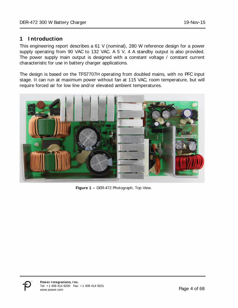
1 Introduction This engineering report describes a 61 V (nominal), 280 W reference design for a power supply operating from 90 VAC to 132 VAC. A 5 V, 4 A standby output is also provided. The power supply main output is designed with a constant voltage / constant current characteristic for use in battery charger applications. The design is based on the TFS7707H operating from doubled mains, with no PFC input stage. It can run at maximum power without fan at 115 VAC, room temperature, but will require forced air for low line and/or elevated ambient temperatures.
Figure 1 – DER-472 Photograph, Top View.

19-Nov-15 DER-472 300 W Battery Charger
Page 5 of 68
Power Integrations Tel: +1 408 414 9200 Fax: +1 408 414 9201
www.power.com
Figure 2 – DER-472 Photograph, Bottom View.
DER-472 300 W Battery Charger 19-Nov-15
Page 6 of 68
Power Integrations, Inc. Tel: +1 408 414 9200 Fax: +1 408 414 9201 www.power.com
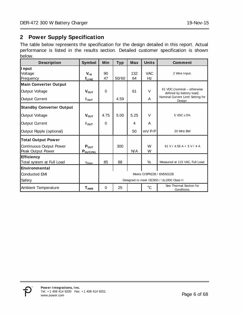
2 Power Supply Specification The table below represents the specification for the design detailed in this report. Actual performance is listed in the results section. Detailed customer specification is shown below.
Description Symbol Min Typ Max Units Comment Input Voltage VIN 90 132 VAC 2 Wire Input.
Frequency fLINE 47 50/60 64 Hz
Main Converter Output
Output Voltage VOUT 0 61 V 61 VDC (nominal – otherwise defined by battery load).
Output Current IOUT 4.59 A Nominal Current Limit Setting for Design.
Standby Converter Output
Output Voltage VOUT 4.75 5.00 5.25 V 5 VDC ±5%
Output Current IOUT 0 4 A
Output Ripple (optional) 50 mV P-P 20 MHz BW
Total Output Power
Continuous Output Power POUT 300 W 61 V / 4.59 A + 5 V / 4 A
Peak Output Power POUT(PK) N/A W
Efficiency
Total system at Full Load ηMain 85 88 % Measured at 115 VAC, Full Load.
Environmental
Conducted EMI Meets CISPR22B / EN55022B
Safety Designed to meet IEC950 / UL1950 Class II
Ambient Temperature TAMB 0 25 oC See Thermal Section for Conditions.

19-Nov-15 DER-472 300 W Battery Charger
Page 7 of 68
Power Integrations Tel: +1 408 414 9200 Fax: +1 408 414 9201
www.power.com
3 Schematic
Figure 3 – Schematic - Forward Battery Charger Application Circuit - Input Filter, FWD Stage, Bias
Supplies and Output Voltage/Current Control.

DER-472 300 W Battery Charger 19-Nov-15
Page 8 of 68
Power Integrations, Inc. Tel: +1 408 414 9200 Fax: +1 408 414 9201 www.power.com
4 Circuit Description
4.1 General Topology The schematic in Figure 3 shows a 2-switch forward power supply with flyback standby utilizing the TFS7707H, powered via a voltage doubler. The secondary control circuitry provides CV/CC control for use in battery charger applications
4.2 EMI Filtering / Voltage Doubler Capacitors C1 and C2 are used to control differential mode noise. Resistors R1-3 discharge C1 and C2 when AC power is removed. Inductors L1 and L2 primarily control common mode EMI, and to some extent, differential mode EMI. The heat sink for U1 is connected to primary return to eliminate the heat sink as a source of radiated/capacitive coupled noise. Thermistor RT1 provides inrush limiting. Capacitors C10 and C26 filter common mode EMI. Capacitors C3 and C4, along with BR1, form a voltage doubler to provide a ~250-380 VDC B+ supply from the 90-132 VAC input. Capacitor C27 provides local HV bypassing for the 5V standby converter.
4.3 Primary Bias Supply The standby supply utilizes built-in capability of the U1 HiperTFS-2 device. Components D15 and C28 provide a 15 V (nominal) flyback bias supply for U1 generated from a primary-referred winding on standby transformer T2. Components D17 and C30 generate a 12 V bias supply for the secondary control circuitry via a secondary-referred winding on T2. Components R42, R44, and VR5-6 clamp the primary and secondary VCC output voltages when the 5 V standby supply is heavily loaded. Components Q3, R31, and C20 comprise a “capacitor multiplier” circuit to provide extra ripple filtering for the secondary VCC supply.
4.4 Main Forward Converter / Standby The schematic in Figures 3 depicts a 61 V, 280 W Forward DC-DC converter with constant voltage/ constant current output implemented using the TFS7707H. Integrated circuit U1 incorporates the control circuitry, drivers and output MOSFETs necessary for a 2-switch forward converter and a flyback standby converter. Components D6, C11, R19-20, and VR4 form a turn-off clamping circuit that limits the standby drain voltage of U1. Zener VR4 provides a defined clamp voltage and maintains a maximum voltage (150 V) on clamp capacitor C11 for higher light/no-load efficiency. Diode D5 provides initial biasing for the main converter high-side driver in U1. Subsequent power is supplied by a winding on T1, rectified and filtered by D3, C6-7 and R15.

19-Nov-15 DER-472 300 W Battery Charger
Page 9 of 68
Power Integrations Tel: +1 408 414 9200 Fax: +1 408 414 9201
www.power.com
The low-side drain of the main output forward converter is clamped by D2, R7, R14, C5, and VR1-3. This clamping scheme is described as “clamp to ground” and enables a wider operating duty cycle for the main forward converter. This in turn allows the turns ratio of main transformer T1 to be dropped (lower peak output voltage), enabling use of lower voltage rating (lower voltage drop) components for forward output rectifier and catch diode D7. The high-side drain is clamped by D5. Most of the leakage and magnetizing energy associated with the main and standby converters is returned back to the B+ supply due to the slow recovery aspect of blocking diodes D2 and D6. During the main converter off-time, the main transformer is reset by a substantially higher voltage than VIN, hence the main converter can operate above 50% duty cycle, lowering RMS switch currents without penalizing holdup time. Use of a clamp to ground snubber for the main converter instead of the usual clamp to rail scheme allows this advantage to be exploited even further. The BYPASS (BP) pin along with C8 provides a decoupled regulated 5.85 V for the HiperTFS-2 controller. The value for C8 (10 µF) also selects the operating frequency of the main converter at 132 kHz. At start-up the bypass capacitor is charged from a current source internal to U1. When the BP pin voltage reaches 5.8 V, the standby converter can begin switching and both the secondary and primary-side bias voltages will begin to rise. Output of the primary bias winding is used to supply power via resistor R5 to the HiperTFS BP pin during standby-only operation. Additional current is provided via current source Q1-2, R4, R6, and D1 by the primary bias supply when remote-on switch SW1 activates U5A and U5B. The value of R4 is selected to satisfy the maximum current requirement of U1. The value of R5 is selected to maintain the minimum 700 µA required into BP pin to inhibit the internal HiperTFS-2 high voltage current source and thus reduce no-load consumption when the main converter is turned off. The ENABLE (EN) pin is the feedback pin for the flyback standby controller section. Prior to start-up a resistor (R16) connected from EN to BP can be detected by the controller to select the internal current limit for standby section. The circuit presented here uses a 107 kΩ resistor (R16) at the EN pin for a standby ILIM of 750 mA (nominal). A capacitor (C9) is placed between EN and G to filter high frequency noise and help prevent pulse bunching, especially at maximum output power. The FEEDBACK (FB) pin has no pull-up resistor to the BP pin, selecting the minimum primary current limit option for the U1 main forward converter. The FB pin provides feedback for the main converter. An increase in current sinking from FB pin to ground will reduce the operating duty cycle.
DER-472 300 W Battery Charger 19-Nov-15
Page 10 of 68
Power Integrations, Inc. Tel: +1 408 414 9200 Fax: +1 408 414 9201 www.power.com
Capacitor C6 is the filtering and charge storage capacitor for the U1 high-side driver. During start-up the high-side MOSFET HS pin of U1 is briefly pulled to Source for 12 ms to precharge C6 using an internal current source. The nominal voltage on C6 during normal operation is shunt regulated to approximately 12 V. Components D3, C7, and R15 provide an efficient alternate source of current from a winding on main transformer T1 to power the high-side driver of U1, so that the internal high voltage supply for the high-side driver is turned off. This increases efficiency at light load and prevents main converter from pulse skipping, especially at light output loads. Resistors R8-10 are used to translate the maximum available OFF time reset voltage into a current for the R pin and compare with the L pin current to compute the maximum allowable duty cycle to prevent saturation and to also determine the maximum allowable duty factor as a function of peak on-time flux. The LINE-SENSE (L) pin provides an input bulk voltage line-sense function. This information is used by the under-voltage and over-voltage detection circuits for both the Main and standby sections. This pin can also be pulled down to Source to implement a remote-ON/OFF for both the standby and main supplies simultaneously. Resistors R11-R13 are used to translate the input voltage into a current for the L pin. Components R50, SW1, and U5 (on the standby converter secondary output) provide remote start. When SW1 is closed, the output transistor of U5 turns on current source Q1-2 on the primary side of the supply, providing operating current to the main converter via the BP pin of U1. Opening SW1 turns off U5, shutting down the main converter function of U1.
4.5 Output Rectification The output of transformer T1 is rectified and filtered by D7, L3, and C13-14. Output rectifier D7 is a 300 V rectifier chosen for high efficiency. A snubber consisting of R21 and C12 helps limit the peak voltage excursion on the output rectifier.
4.6 Output Current and Voltage Control Output current is sensed via resistors R39 and R40. These resistors are clamped by diode D14 to avoid damage to the current control circuitry during an output short-circuit. Components R32 and U2 provide a voltage reference for current sense and voltage sense amplifiers U3A and U3B. The reference voltage for current sense amplifier U3A is divided down by R34-35 and R38. The default current limit setting is 4.589 A, as programmed by R39-40, R34-35, and R38. Voltage from the current sense resistors is applied to the inverting input of U3A via R36. Opamp U3A drives optocoupler U4 through D8 and R23. Components R23, R33, R36, R37, C23, and C25 are used for frequency compensation of the current loop.
19-Nov-15 DER-472 300 W Battery Charger
Page 11 of 68
Power Integrations Tel: +1 408 414 9200 Fax: +1 408 414 9201
www.power.com
Opamp U3B is used for output constant voltage control when the current limit is not engaged. Resistors R27 and R29 sense the output voltage. A reference voltage is applied to the non-inverting input of U3B from U2 via R30 and C19. Opamp U3B drives optocoupler U4 via D9 and R24. Components R24-26 and C16-C17 all affect the frequency compensation of the voltage control loop. Networks R28, C18, and D10-D11, along with R22, C15, and D12-D13, are used as soft-finish networks to reduce output voltage and/or output current overshoot during startup. Capacitor C15 on the current soft finish network has been reduced to a very small placeholder value (47 pF) in order to disable the current soft-finish function for this design. The networks can be eliminated if main output start-up overshoot is not a concern.
4.7 Standby Output A 5 V, 4 A standby output is provided via a triple insulated winding on standby transformer T2. This winding is rectified and filtered by D16, and C31-32. Components L4 and C35 provide additional filtering to remove high frequency ripple and noise. Snubber C29 and R43 helps limit the peak voltage excursion on D16. The 5 V output is divided down by R49 and R51, and is applied to the reference input of error amplifier U7, which controls the standby section of U1 via R45 and U6. Resistor R46 provides bias current to U7, while C33 and R47 comprise a soft-finish network to eliminate output voltage overshoot at start-up. Components R45, R48, and C34 compensate the standby control loop.
DER-472 300 W Battery Charger 19-Nov-15
Page 12 of 68
Power Integrations, Inc. Tel: +1 408 414 9200 Fax: +1 408 414 9201 www.power.com
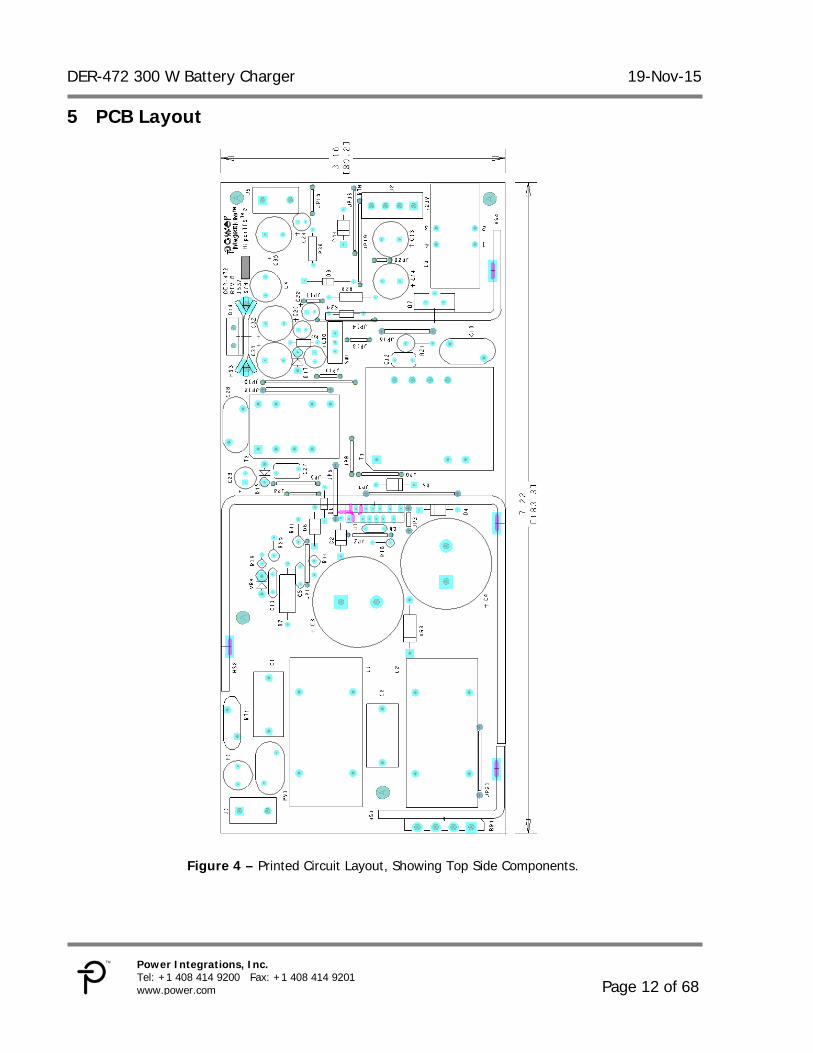
5 PCB Layout
Figure 4 – Printed Circuit Layout, Showing Top Side Components.

19-Nov-15 DER-472 300 W Battery Charger
Page 13 of 68
Power Integrations Tel: +1 408 414 9200 Fax: +1 408 414 9201
www.power.com
Figure 5 – Printed Circuit Layout, Bottom Side Traces and Components.

DER-472 300 W Battery Charger 19-Nov-15
Page 14 of 68
Power Integrations, Inc. Tel: +1 408 414 9200 Fax: +1 408 414 9201 www.power.com
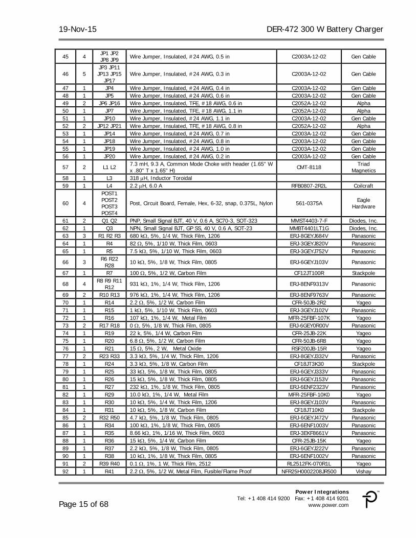
6 Bill of Materials Item Qty Ref Des Description Mfg Part Number Mfg
1 1 BR1 600 V, 8 A, Bridge Rectifier, GBU Case GBU8J-BP Micro Commercial
2 1 C1 220 nF, 275 VAC, Film, X2 ECQ-U2A224ML Panasonic 3 1 C2 470 nF, 275 VAC, Film, X2 80-R46KI347050P1M Kemet 4 2 C3 C4 680 µF, 200 V, Electrolytic, (25 x 40) LGY2D681MELA Nichicon 5 1 C5 2.2 nF, 1 KV, Ceramic, SL, 0.2" L.S. DEBB33A222KA2B Murata 6 2 C6 C7 100 nF 50 V, Ceramic, X7R, 0603 C1608X7R1H104K TDK 7 1 C8 10 µF, 16 V, Ceramic, X5R FK24X5R1C106K TDK 8 1 C9 220 pF, 250 V, Ceramic, COG, 0603 C1608C0G2E221J TDK 9 2 C10 C26 4.7 nF, Ceramic, Y1 440LD47-R Vishay 10 1 C11 2.2 nF, 1 kV, Disc Ceramic NCD222K1KVY5FF NIC 11 1 C12 47 pF, 1 kV, Disc Ceramic 561R10TCCQ47 Vishay 12 2 C13 C14 150 µF, 80 V, Electrolytic, Gen. Purpose, (10 x 33) UPJ1K151MPD Nichicon 13 1 C15 47 pF, 100 V, Ceramic, COG, 0805 08051A470JAT2A Kemet 14 1 C16 680 pF 100 V, Ceramic, NPO, 0603 CGA3E2C0G2A681J TDK 15 2 C17 C19 10 nF, 200 V, Ceramic, X7R, 0805 08052C103KAT2A AVX 16 2 C18 C25 15 nF, 50 V, Ceramic, X7R, 0805 CC0805KRX7R9BB153 Yageo
17 3 C20 C22 C24 10 µF, 50 V, Electrolytic, Gen. Purpose, (5 x 11) EKMG500ELL100ME11D Nippon Chemi-
Con 18 1 C21 100 nF, 50 V, Ceramic, X7R, 0805 CC0805KRX7R9BB104 Yageo 19 1 C23 47 nF, 50 V, Ceramic, X7R, 0805 GRM21BR71H473KA01L Murata 20 1 C27 1.0 nF, 1 kV, Disc Ceramic 562R10TSD10 Vishay
21 2 C28 C30 100 µF, 35 V, Electrolytic, Low ESR, 180 mΩ, (6.3 x 15) ELXZ350ELL101MF15D Nippon Chemi-Con
22 1 C29 1 nF, 200 V, Ceramic, X7R, 0805 08052C102KAT2A AVX 23 2 C31 C32 1200 µF, 10 V, Electrolytic, Radial EEU-FM1A122 Panasonic 24 1 C33 2.2 µF, 25 V, Ceramic, X7R, 0805 C2012X7R1E225M TDK 25 1 C34 330 nF, 50 V, Ceramic, X7R, 0805 GRM219R71H334KA88 Murata
26 1 C35 330 µF, 25 V, Electrolytic, Low ESR, 90 mΩ, (10 x 12.5) ELXZ250ELL331MJC5S Nippon Chemi-Con
27 2 D1 D8 75 V, 300 mA, Fast Switching, DO-35 1N4148TR Vishay 28 2 D2 D6 1000 V, 1 A, Rectifier, DO-41 1N4007-E3/54 Vishay 29 1 D3 Diode Ultrafast, SW, 200 V, 1 A, SMA US1D-13-F Diodes, Inc. 30 2 D4 D5 600 V, 1 A, Ultrafast Recovery, 75 ns, DO-41 UF4005-E3 Vishay 31 1 D7 300 V, 10 A, Diode ARRAY, GP, 35 ns, TO-220AB STTH2003CT ST Micro
32 5 D9 D10 D11 D12
D13 100 V, 0.2 A, Fast Switching, 50 ns, SOD-323 BAV19WS-7-F Diodes, Inc.
33 1 D14 100 V, 1 A, Rectifier, DO-41 1N4002-E3/54 Vishay 34 2 D15 D17 200 V, 1 A, Ultrafast Recovery, 50 ns, DO-41 UF4003-E3 Vishay 35 1 D16 45 V, 10 A, Schottky, TO-220AC MBR1045 Vishay
36 1 ESIP CLIP1 Heat Sink Hardware, Edge Clip, 12.40 mm x 6.50 mm TRK-24 Kang Tang
37 1 F1 5 A, 250 V, Slow, TR5 37215000411 Wickman
38 1 HOTMELT_V1 Adhesive, Hot Melt, VO 3748 VO-TC 3M
39 1 HS1 FAB, Heat Sink, BRIDGE, DER-472 Custom 40 1 HS2 FAB, Heat Sink, eSIP, DER-472 Custom
41 1 HS3 Heat Sink, TO-220, Copper base, staggered, Vertical 6025DG Aavid Thermalloy
42 1 HS4 FAB, Heat Sink, DIODE, DER-472 Custom 43 2 J1 J5 3 Position (1 x 3) header, 0.156 pitch, Vertical 26-48-1031 Molex 44 1 J2 4 Position (1 x 4) header, 0.156 pitch, Vertical 26-48-1045 Molex
19-Nov-15 DER-472 300 W Battery Charger
Page 15 of 68
Power Integrations Tel: +1 408 414 9200 Fax: +1 408 414 9201
www.power.com
45 4 JP1 JP2 JP8 JP9 Wire Jumper, Insulated, #24 AWG, 0.5 in C2003A-12-02 Gen Cable
46 5 JP3 JP11 JP13 JP15
JP17 Wire Jumper, Insulated, #24 AWG, 0.3 in C2003A-12-02 Gen Cable
47 1 JP4 Wire Jumper, Insulated, #24 AWG, 0.4 in C2003A-12-02 Gen Cable 48 1 JP5 Wire Jumper, Insulated, #24 AWG, 0.6 in C2003A-12-02 Gen Cable 49 2 JP6 JP16 Wire Jumper, Insulated, TFE, #18 AWG, 0.6 in C2052A-12-02 Alpha 50 1 JP7 Wire Jumper, Insulated, TFE, #18 AWG, 1.1 in C2052A-12-02 Alpha 51 1 JP10 Wire Jumper, Insulated, #24 AWG, 1.1 in C2003A-12-02 Gen Cable 52 2 JP12 JP21 Wire Jumper, Insulated, TFE, #18 AWG, 0.8 in C2052A-12-02 Alpha 53 1 JP14 Wire Jumper, Insulated, #24 AWG, 0.7 in C2003A-12-02 Gen Cable 54 1 JP18 Wire Jumper, Insulated, #24 AWG, 0.8 in C2003A-12-02 Gen Cable 55 1 JP19 Wire Jumper, Insulated, #24 AWG, 1.0 in C2003A-12-02 Gen Cable 56 1 JP20 Wire Jumper, Insulated, #24 AWG, 0.2 in C2003A-12-02 Gen Cable
57 2 L1 L2 7.3 mH, 9.3 A, Common Mode Choke with header (1.65" W x .80" T x 1.65" H) CMT-8118 Triad
Magnetics 58 1 L3 318 µH, Inductor Toroidal 59 1 L4 2.2 µH, 6.0 A RFB0807-2R2L Coilcraft
60 4
POST1 POST2 POST3 POST4
Post, Circuit Board, Female, Hex, 6-32, snap, 0.375L, Nylon 561-0375A Eagle Hardware
61 2 Q1 Q2 PNP, Small Signal BJT, 40 V, 0.6 A, SC70-3, SOT-323 MMST4403-7-F Diodes, Inc. 62 1 Q3 NPN, Small Signal BJT, GP SS, 40 V, 0.6 A, SOT-23 MMBT4401LT1G Diodes, Inc. 63 3 R1 R2 R3 680 kΩ, 5%, 1/4 W, Thick Film, 1206 ERJ-8GEYJ684V Panasonic 64 1 R4 82 Ω, 5%, 1/10 W, Thick Film, 0603 ERJ-3GEYJ820V Panasonic 65 1 R5 7.5 kΩ, 5%, 1/10 W, Thick Film, 0603 ERJ-3GEYJ752V Panasonic
66 3 R6 R22 R28 10 kΩ, 5%, 1/8 W, Thick Film, 0805 ERJ-6GEYJ103V Panasonic
67 1 R7 100 Ω, 5%, 1/2 W, Carbon Film CF12JT100R Stackpole
68 4 R8 R9 R11 R12 931 kΩ, 1%, 1/4 W, Thick Film, 1206 ERJ-8ENF9313V Panasonic
69 2 R10 R13 976 kΩ, 1%, 1/4 W, Thick Film, 1206 ERJ-8ENF9763V Panasonic 70 1 R14 2.2 Ω, 5%, 1/2 W, Carbon Film CFR-50JB-2R2 Yageo 71 1 R15 1 kΩ, 5%, 1/10 W, Thick Film, 0603 ERJ-3GEYJ102V Panasonic 72 1 R16 107 kΩ, 1%, 1/4 W, Metal Film MFR-25FBF-107K Yageo 73 2 R17 R18 0 Ω, 5%, 1/8 W, Thick Film, 0805 ERJ-6GEY0R00V Panasonic 74 1 R19 22 k, 5%, 1/4 W, Carbon Film CFR-25JB-22K Yageo 75 1 R20 6.8 Ω, 5%, 1/2 W, Carbon Film CFR-50JB-6R8 Yageo 76 1 R21 15 Ω, 5%, 2 W, Metal Oxide RSF200JB-15R Yageo 77 2 R23 R33 3.3 kΩ, 5%, 1/4 W, Thick Film, 1206 ERJ-8GEYJ332V Panasonic 78 1 R24 3.3 kΩ, 5%, 1/8 W, Carbon Film CF18JT3K30 Stackpole 79 1 R25 33 kΩ, 5%, 1/8 W, Thick Film, 0805 ERJ-6GEYJ333V Panasonic 80 1 R26 15 kΩ, 5%, 1/8 W, Thick Film, 0805 ERJ-6GEYJ153V Panasonic 81 1 R27 232 kΩ, 1%, 1/8 W, Thick Film, 0805 ERJ-6ENF2323V Panasonic 82 1 R29 10.0 kΩ, 1%, 1/4 W, Metal Film MFR-25FBF-10K0 Yageo 83 1 R30 10 kΩ, 5%, 1/4 W, Thick Film, 1206 ERJ-8GEYJ103V Panasonic 84 1 R31 10 kΩ, 5%, 1/8 W, Carbon Film CF18JT10K0 Stackpole 85 2 R32 R50 4.7 kΩ, 5%, 1/8 W, Thick Film, 0805 ERJ-6GEYJ472V Panasonic 86 1 R34 100 kΩ, 1%, 1/8 W, Thick Film, 0805 ERJ-6ENF1003V Panasonic 87 1 R35 8.66 kΩ, 1%, 1/16 W, Thick Film, 0603 ERJ-3EKF8661V Panasonic 88 1 R36 15 kΩ, 5%, 1/4 W, Carbon Film CFR-25JB-15K Yageo 89 1 R37 2.2 kΩ, 5%, 1/8 W, Thick Film, 0805 ERJ-6GEYJ222V Panasonic 90 1 R38 10 kΩ, 1%, 1/8 W, Thick Film, 0805 ERJ-6ENF1002V Panasonic 91 2 R39 R40 0.1 Ω, 1%, 1 W, Thick Film, 2512 RL2512FK-070R1L Yageo 92 1 R41 2.2 Ω, 5%, 1/2 W, Metal Film, Fusible/Flame Proof NFR25H0002208JR500 Vishay

DER-472 300 W Battery Charger 19-Nov-15
Page 16 of 68
Power Integrations, Inc. Tel: +1 408 414 9200 Fax: +1 408 414 9201 www.power.com
93 4 R42 R44 R46 R48 1 kΩ, 5%, 1/8 W, Thick Film, 0805 ERJ-6GEYJ102V Panasonic
94 1 R43 4.7 Ω, 5%, 1/4 W, Thick Film, 1206 ERJ-8GEYJ4R7V Panasonic 95 1 R45 100 Ω, 5%, 1/8 W, Thick Film, 0805 ERJ-6GEYJ101V Panasonic 96 1 R47 680 Ω, 5%, 1/8 W, Thick Film, 0805 ERJ-6GEYJ681V Panasonic 97 2 R49 R51 4.99 kΩ, 1%, 1/8 W, Thick Film, 0805 ERJ-6ENF4991V Panasonic 98 1 RT1 NTC Thermistor, 2.5 Ohms, 7 A SL15 2R507 Ametherm
99 2 RTV1 RTV2 Thermally conductive Silicone Grease 120-SA Wakefield
100 1 RV1 175 V, 70 J, 14 mm, RADIAL ERZ-V14D271 Panasonic
101 1 SCREW1 SCREW MACHINE PHIL 4-40 X 1/4 SS PMSSS 440 0025 PH Building Fasteners
102 1 SCREW2 SCREW MACHINE PHIL 4-40X 3/16 SS 67413609 MSC Industrial
103 1 SCREW3 SCREW MACHINE PHIL 4-40 X 5/16 SS PMSSS 440 0031 PH Building Fasteners
104 2
SPACER_CER1
SPACER_CER2
SPACER RND, Steatite C220 Ceramic CER-2 Richco
105 1 SW1 SWITCH SLIDE SPDT 30 V. 2 A PC MNT EG1218 E-Switch 106 1 T1 Transformer, EER35, Vertical, 14 pins Custom 107 1 T2 Transformer, EF25/13/7, Vertical, 10 pins Custom
108 1 TO-220 PAD1 THERMAL PAD TO-220 .009" SP1000 1009-58 Bergquist
109 1 U1 HiperTFS-2, ESIP16/12 TFS7707H Power Integrations
110 1 U2 IC, REG ZENER SHUNT ADJ SOT-23 LM431BIM3/NOPB National Semi 111 1 U3 DUAL Op Amp, LM358ADR2G, Single Supply, SOIC-8 LM358ADR2G ON Semi 112 3 U4 U5 U6 Optocoupler, 80 V, CTR 80-160%, 4-Mini Flat PC357N1TJ00F Sharp 113 1 U7 IC, REG ZENER SHUNT ADJ SOT-23 LM431AIM3/NOPB National Semi 114 2 VR1 VR2 150 V, 5 W, 5%, DO214AA (SMB) SMBJ150A Littlefuse 115 1 VR3 170 V, 5 W, 5%, TVS, DO204AC (DO-15) P6KE170A Littlefuse 116 1 VR4 150 V, 5 W, 5%, TVS, DO204AC (DO-15) P6KE150A Littlefuse 117 2 VR5 VR6 Diode Zener 18 V 500 MW SOD123 MMSZ5248B-7-F Diodes, Inc.
118 1 WASHER1 WASHER FLAT #4 SS FWSS 004 Building Fasteners
119 2 WASHER2 WASHER4
WASHER FLAT #4 Zinc, OD 0.219, ID 0.125, Thk 0.032, Yellow Chromate Finish 5205820-2 Tyco
120 1 WASHER3 Washer, Shoulder, #4, 0.032 Shoulder x 0.116" Dia, Polyphenylene Sulfide PPS 7721-7PPSG Aavid
Thermalloy
19-Nov-15 DER-472 300 W Battery Charger
Page 17 of 68
Power Integrations Tel: +1 408 414 9200 Fax: +1 408 414 9201
www.power.com
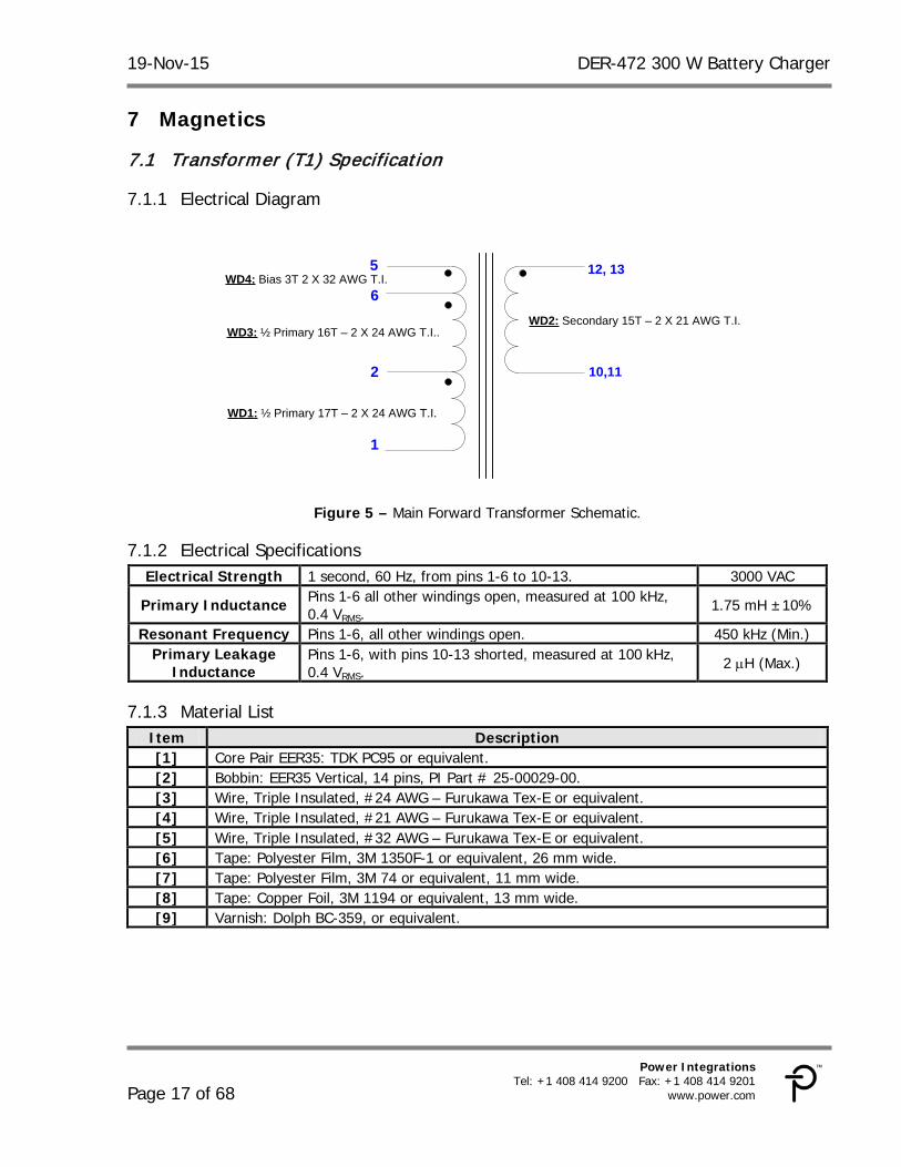
7 Magnetics
7.1 Transformer (T1) Specification
Electrical Diagram 7.1.1
5
2
12, 13
10,11
WD1: ½ Primary 17T – 2 X 24 AWG T.I.
WD2: Secondary 15T – 2 X 21 AWG T.I.WD3: ½ Primary 16T – 2 X 24 AWG T.I..
WD4: Bias 3T 2 X 32 AWG T.I.
1
6
Figure 5 – Main Forward Transformer Schematic.
Electrical Specifications 7.1.2Electrical Strength 1 second, 60 Hz, from pins 1-6 to 10-13. 3000 VAC
Primary Inductance Pins 1-6 all other windings open, measured at 100 kHz, 0.4 VRMS.
1.75 mH ±10%
Resonant Frequency Pins 1-6, all other windings open. 450 kHz (Min.) Primary Leakage
Inductance Pins 1-6, with pins 10-13 shorted, measured at 100 kHz, 0.4 VRMS.
2 µH (Max.)
Material List 7.1.3Item Description [1] Core Pair EER35: TDK PC95 or equivalent. [2] Bobbin: EER35 Vertical, 14 pins, PI Part # 25-00029-00. [3] Wire, Triple Insulated, #24 AWG – Furukawa Tex-E or equivalent. [4] Wire, Triple Insulated, #21 AWG – Furukawa Tex-E or equivalent. [5] Wire, Triple Insulated, #32 AWG – Furukawa Tex-E or equivalent. [6] Tape: Polyester Film, 3M 1350F-1 or equivalent, 26 mm wide. [7] Tape: Polyester Film, 3M 74 or equivalent, 11 mm wide. [8] Tape: Copper Foil, 3M 1194 or equivalent, 13 mm wide. [9] Varnish: Dolph BC-359, or equivalent.

DER-472 300 W Battery Charger 19-Nov-15
Page 18 of 68
Power Integrations, Inc. Tel: +1 408 414 9200 Fax: +1 408 414 9201 www.power.com
Build Diagram 7.1.4
WD1: ½ Pri 17T – 2 X #24 AWG T.I.
WD2: Sec 15T – 2 X #21 AWG T.I.
WD3: ½ Pri 16T – 2 X #24 AWG T. I.
WD4: Bias 3T – 2 X #32 AWG T.I.
21
12, 13
62
65
10, 11
Figure 6 – Transformer Build Diagram.
Winding Instructions 7.1.5
General note For the purpose of these instructions, bobbin is oriented on winder such that pins 1-7 are on the left side (see illustration). Winding direction as shown is clockwise.
WD1: ½ Primary
Starting on pin 2, wind 17 bifilar turns of triple insulated wire item [3] in 1 layer, finish on pin 1.
Insulation Apply 2 layers of tape item [6].
WD2: Secondary
Starting at pins 12 and 13, wind 12 bifilar turns of triple insulated wire item [4] in one layer. Wind remaining 3 turns back evenly across bobbin width, finishing at pins 10 and 11.
Insulation Apply 2 layers of tape item [6].
WD3: ½ Primary
Starting on pin 6, wind 16 bifilar turns of triple insulated wire item [3] in 1 layer, and finish on pin 2.
Insulation Apply 2 layers of tape item [6].
WD4: Bias Starting at pin 5, wind 3 bifilar turns of triple insulated wire [5] finish on pin 6.
Insulation Apply 3 layers of tape item [6].
Core Gapping Apply tape shim gap item [7] to mating faces of one core half as shown. Polish core faces against flat surface to remove air bubbles from tape and assure minimum possible gap.
Assembly (1)
Assemble gapped and ungapped core halves in bobbin, secure with tape. Using copper tape item [8], apply an outside flux band centered in the bobbin window as shown in illustration. Overlap and solder ends of band to form a shorted turn. Attach wire item [5] to copper band and terminate to pin 7.
Assembly (2) Apply 1 layer of tape item [6] around transformer as shown to insulate flux band. Remove pins 3, 4, 8, 9, and 14. Cut pin 2 short. Dip varnish [9].
19-Nov-15 DER-472 300 W Battery Charger
Page 19 of 68
Power Integrations Tel: +1 408 414 9200 Fax: +1 408 414 9201
www.power.com
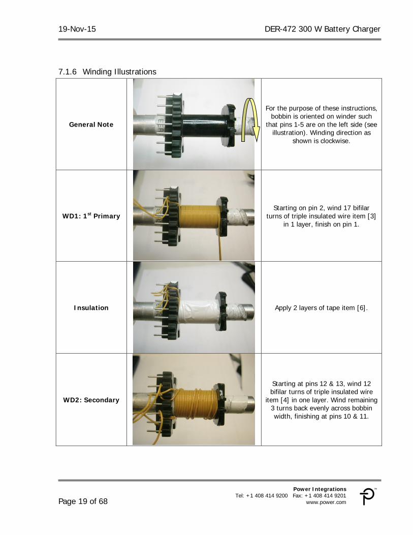
Winding Illustrations 7.1.6
General Note
For the purpose of these instructions, bobbin is oriented on winder such
that pins 1-5 are on the left side (see illustration). Winding direction as
shown is clockwise.
WD1: 1st Primary
Starting on pin 2, wind 17 bifilar turns of triple insulated wire item [3]
in 1 layer, finish on pin 1.
Insulation
Apply 2 layers of tape item [6].
WD2: Secondary
Starting at pins 12 & 13, wind 12 bifilar turns of triple insulated wire
item [4] in one layer. Wind remaining 3 turns back evenly across bobbin width, finishing at pins 10 & 11.
DER-472 300 W Battery Charger 19-Nov-15
Page 20 of 68
Power Integrations, Inc. Tel: +1 408 414 9200 Fax: +1 408 414 9201 www.power.com
Insulation
Apply 2 layers of tape item [6].
WD3: ½ Primary
Starting on pin 6, wind 16 bifilar turns of triple insulated wire item [3]
in 1 layer, and finish on pin 2.
Insulation
Apply 2 layers of tape item [6].
WD4: Bias
Starting at pin 5, wind 3 bifilar turns of triple insulated wire [5] finish on
pin 6.

19-Nov-15 DER-472 300 W Battery Charger
Page 21 of 68
Power Integrations Tel: +1 408 414 9200 Fax: +1 408 414 9201
www.power.com
Insulation
Apply 3 layers of tape item [6].
Core Gapping
Apply tape shim gap item [7] to mating faces of one core half as
shown. Polish core faces against flat surface to remove air bubbles from tape and assure minimum possible
gap.
Assembly (1)
Assemble gapped and ungapped core halves in bobbin, secure with tape.
Using copper tape item [8], apply an outside flux band centered in the
bobbin window as shown in illustration. Overlap and solder ends
of band to form a shorted turn. Attach wire item [5] to copper band
and terminate to pin 7.
Assembly (2)
Apply 1 layer of tape item [6] around transformer as shown to insulate flux band. Remove pins 3, 4, 8, 9, and 14.
Cut pin 2 short. Dip varnish [9].
DER-472 300 W Battery Charger 19-Nov-15
Page 22 of 68
Power Integrations, Inc. Tel: +1 408 414 9200 Fax: +1 408 414 9201 www.power.com
7.2 Standby Transformer (T2) Specification
Electrical Diagram 7.2.1
4
5
7
61
2
WD1: 1st Primary39T – #28 AWG
WD4: Sec Bias9T – #32 AWG_T.I.
WD2: PBias12T – #32 AWG T.I.
WD5: 2nd primary34T – #28 AWG
3
WD3: SBY Out4T – 2 X 23 AWG_T.I
10
9
Figure 7 – Transformer Electrical Diagram.
Electrical Specifications 7.2.2Electrical Strength 1 second, 60 Hz, from pins 1-5 to 6-10. 3000 V
Primary Inductance Pins 4-3, all other windings open, measured at 100 kHz, 0.4 VRMS.
1074 µH ±10%
Resonant Frequency Pins 4-3, all other windings open. 600 kHz (Min.) Primary Leakage
Inductance Pins 4-3, with pins 9-10 shorted, measured at 100 kHz, 0.4 VRMS.
30 µH (Max.)
Material List 7.2.3Item Description
[1] Core: EF25, TDK PC44 material or equivalent. Gap for inductance coefficient (AL) of 202 nH/T².
[2] Bobbin, EF25, Vertical, 10 Pins (5/5), PI Part # 25-00012-00. [3] Tape, Polyester film, 3M 1350F-1 or equivalent, 16.4 mm wide. [4] Tape, Polyester film, 3M 1350F-1 or equivalent, 14.9 mm wide. [5] Tape, Polyester web, 3M 44 or equivalent, 1.5 mm wide. [6] Wire, Magnet #28 AWG, solderable double coated. [7] Wire, Triple Insulated, Furukawa TEX-E or equivalent, #23 AWG. [8] Wire, Triple Insulated, Furukawa TEX-E or equivalent, #32 AWG. [9] Transformer Varnish, Dolph BC-359 or equivalent.
19-Nov-15 DER-472 300 W Battery Charger
Page 23 of 68
Power Integrations Tel: +1 408 414 9200 Fax: +1 408 414 9201
www.power.com
Build Diagram 7.2.4
WD1: 1st Primary 39T – #28 AWG
WD2: Bias 12T – #32 AWG T.I.
WD3: Secondary 4T – 2 X #23 AWG T. I.
WD4: Sec. Bias 9 T – #32 AWG T.I.
45
2
1
109
67
35
WD5: 2nd primary 34 T – #28 AWG
1.5mm Margin Tape
1.5mm Margin Tape
Figure 8 – Transformer Build Diagram.
Winding Instructions 7.2.5
General Note For the purpose of these instructions, bobbin is oriented on winder such that pins 1-5 are on the left side (see illustration). Winding direction as shown is clockwise.
Margin Apply 1.5 mm margin on pins side of bobbin using tape [5]. Match height of WDG 1 WD1: 1st Primary Starting at pin 4, wind 39 turns of wire item [6] in 1 layer. Finish at pin 5.
Insulation Use 1 layer of tape item [3] for insulation. WD2: Primary
Bias Starting at pin 2, wind 12 turns of triple insulated wire item [8] in one layer. Finish at pin 1.
Insulation Use 2 layers of tape item [3] for insulation. WD3:
Secondary Starting at pin 10, wind 4 bifilar turns of triple insulated wire item [4] in one layer. Finish at pin 9.
Insulation Use 1 layer of tape item [3] for insulation. WD4:
Secondary Bias Starting at pin 7, wind 9 turns of triple insulated wire item [8] in one layer. Finish at pin 6.
Insulation Use 2 layers of tape item [3] for insulation. Margin Apply 1.5 mm margin on pins side of bobbin using tape [5]. Match height of WDG 5.
WD5: 2nd Primary Starting at pin 5, wind 34 turns of wire item [6] in 1 layer. Finish at pin 3.
Insulation Use 3 layers of tape item [3] to secure the windings.
Assembly
Grind core halves for specified primary inductance. Wrap one core half with 2 layers of tape item [4] as shown in Figure 11. Insert this core in pin side of bobbin. Secure core halves with tape. Remove pin 8, cut pin 5 short. Dip varnish item [9].

DER-472 300 W Battery Charger 19-Nov-15
Page 24 of 68
Power Integrations, Inc. Tel: +1 408 414 9200 Fax: +1 408 414 9201 www.power.com
Winding Illustrations 7.2.6
General Note
For the purpose of these instructions, bobbin is oriented on winder such that pins 1-5
are on the left side (see illustration). Winding direction
as shown is clockwise.
Margin
Apply 1.5 mm margin on pins side of bobbin using tape [5]. Match height of WDG 1 & 2.
WD1: 1st Primary
Starting at pin 4, wind 39 turns of wire item [6] in 1 layer.
Finish at pin 5.

19-Nov-15 DER-472 300 W Battery Charger
Page 25 of 68
Power Integrations Tel: +1 408 414 9200 Fax: +1 408 414 9201
www.power.com
Insulation
Use 1 layer of tape item [3] for insulation.
WD2: Primary Bias
Starting at pin 2, wind 12 turns of triple insulated wire item [8]
in one layer. Finish at pin 1.
Insulation
Use 2 layers of tape item [3] for insulation.

DER-472 300 W Battery Charger 19-Nov-15
Page 26 of 68
Power Integrations, Inc. Tel: +1 408 414 9200 Fax: +1 408 414 9201 www.power.com
WD3: Secondary
Starting at pin 10, wind 4 bifilar turns of triple insulated
wire item [4] in one layer. Finish at pin 9.
Insulation
Use 1 layer of tape item [3] for insulation.
WD4: Secondary Bias
Starting at pin 7, wind 9 turns of triple insulated wire item [8]
in one layer. Finish at pin 6.

19-Nov-15 DER-472 300 W Battery Charger
Page 27 of 68
Power Integrations Tel: +1 408 414 9200 Fax: +1 408 414 9201
www.power.com
Insulation
Use 2 layers of tape item [3] for insulation.
Margin
Apply 1.5 mm margin on pins side of bobbin using tape [5].
Match height of WDG 5.
WD5: 2nd Primary
Starting at pin 5, wind 34 turns of wire item [6] in 1 layer.
Finish at pin 3.
Insulation
Use 3 layers of tape item [3] to secure the windings.

DER-472 300 W Battery Charger 19-Nov-15
Page 28 of 68
Power Integrations, Inc. Tel: +1 408 414 9200 Fax: +1 408 414 9201 www.power.com
Assembly
Grind core halves for specified primary inductance.
Wrap one core half with 2 layers of tape item [4] as
shown in Figure 11. Insert this core in pin side of bobbin.
Secure core halves with tape. Remove pin 8, cut pin 5 short.
Dip varnish item [9].
7mm
19-Nov-15 DER-472 300 W Battery Charger
Page 29 of 68
Power Integrations Tel: +1 408 414 9200 Fax: +1 408 414 9201
www.power.com
7.3 Output Choke
Schematic 7.3.1
FL1&2
WD1: 45T – 2 X 20 AWG
FL 3&4
Inductance – 318 uH +/- 10%
Figure 9 – Output Choke Schematic.
Material List 7.3.2 Description
[1] Core: Sendust Toroid 125µ, 27.7 mm diameter, Mag-Inc 77930-A7 or equivalent. [4] Wire, Magnet, #20 AWG, solderable double coated.
Winding Illustration 7.3.3
Figure 10 – Finished Output Choke.

DER-472 300 W Battery Charger 19-Nov-15
Page 30 of 68
Power Integrations, Inc. Tel: +1 408 414 9200 Fax: +1 408 414 9201 www.power.com
8 Transformer/Inductor Design Spreadsheet The main transformer design shown in this spreadsheet was refined by measuring the actual minimum B+ value at 90 VAC, 100% load (measured at the bottom of the ripple trough) and entering it as the VMIN value in the “Input Voltage and UV/OV” section of the spreadsheet. HiperTFS2_Two-switch_Forward_041114; Rev.2.0; Copyright Power Integrations 2013
INPUT INFO OUTPUT UNIT HiperTFS2_041114_Rev2-0.xls; Two-switch Forward Transformer Design Spreadsheet
Hiper-TFS MAIN OUTPUT (TWO-SWITCH FORWARD STAGE) OUTPUT VOLTAGE AND CURRENT VMAIN 61.00 61.00 V Main output voltage IMAIN 4.59 4.59 A Main output current
VOUT2 0.00 V Output2 voltage - enter zero or leave blank if none
IOUT2 0.00 A Output2 current - enter zero or leave blank if none
Post Regulated Output
Post Regulator NONE NONE Select post regulator from Mag-Amp, Buck, or NONE
V_SOURCE NONE NONE V Select source of input voltage for post regulator. Enter None if Post regulator not used.
VOUT3 0.00 V Enter post regulator output voltage. Enter zero or leave blank if none
IOUT3 0.00 A Enter post regulator output current. Enter zero or leave blank if none
n_PR 1.00 Enter post regulator efficiency (Buck only) Coupled Inductor (Low Power) derived output
VOUT4 0.00 V Output choke derived (low power) output voltage (typically -12 V)
IOUT4 0.00 A Output choke derived (low power) output current
System Power POUT(Main) 280.0 W Total output power (Main converter)
POUT_PEAK(Main) 280.0 280.0 W Peak Output power (Main converter). If there is no peak power requirement enter value equal to continuous power
POUT(Standby) 20.3 W Continuous output power from Standby power supply
POUT_PEAK(Standby) 20.3 W Peak output power from Standby section below
POUT(System Total) 300.3 W Total system continuous output power
POUT_PEAK(System Total) 300.3 W Total system peak output power INPUT VOLTAGE AND UV/OV
CIN_MIN 253 uF Minimum Input Capacitance to meet holdup time. To increase CMIN, increase T_HOLDUP
T_HOLDUP 20.0 ms Holdup time CIN_ACTUAL 330 330 uF Select Actual Bulk Capacitor CIN_ESR 0.25 Ω Bulk capacitor ESR IRMS_CIN 1.13 A RMS current through bulk capacitor PLOSS_CIN 0.32 W Bulk capacitor ESR losses
VMIN 220 220 V Minimum input voltage to guarantee output regulation at full load
VNOM 322 322 V Nominal input voltage VMAX 392 V Maximum DC input voltage

19-Nov-15 DER-472 300 W Battery Charger
Page 31 of 68
Power Integrations Tel: +1 408 414 9200 Fax: +1 408 414 9201
www.power.com
RR 3.32 MΩ R pin resistor
RL 3.32 MΩ Line Sense resistor value (L-pin) - goal seek (VUV OFF) for std 1% resistor series
UV and OV thresholds Clamp Section
Clamp Selection CLAMP TO GND Select either "CLAMP TO RAIL" (default)
or "CLAMP TO GND" VCLAMP 530 V Asymmetric Clamp Zener Voltage
VDSOP 530 V Estimated Maximum Hiper-TFS Drain voltage (at VOVOFF_MAX)
DUTY CYCLE VALUES (REGULATION) DVMIN 0.67 Duty cycle at minimum DC input voltage
DVNOM_GOAL 0.46 Target duty cycle at nominal input voltage (VNOM)
DVNOM 0.45 Duty cycle at nominal DC input voltage DVMAX 0.37 Duty cycle at maximum DC input voltage
DOVOFF MIN 0.37 Duty cycle at over-voltage DC input voltage (DOVOFF_MIN)
Maximum Duty Cycle values DMAX_UVOFF_MIN 0.78 Max duty cycle clamp at VUVOFF_MIN DMAX_VMIN 0.71 Max duty clamp cycle at VMIN DMAX_VNOM 0.56 Max duty clamp cycle at VNOM DMAX_VMAX 0.46 Max duty clamp cycle at VMAX DMAX_OVOFFMIN 0.46 Max duty clamp cycle at VOVOFF_MAX DEVICE VARIABLES Device TFS7707 TFS7707 Selected HiperTFS device Select Frequency mode Auto 132 kHz Select Frequency mode. ILIMIT_MIN 4.36 A Device current limit (Minimum) ILIMIT_TYP 4.69 A Device current limit (Typical) ILIMIT_MAX 5.02 A Device current limit (Maximum) fSMIN 124,000 Hz Device switching frequency (Minimum) fS 132,000 Hz Device switching frequency (Typical) fSMAX 140,000 Hz Device switching frequency (Maximum)
KI 0.7 0.7 Select Current limit factor (KI=1.0 for default ILIMIT, or select KI=0.9 or KI=0.7)
R(FB) 1740 kΩ Feedback Pin Resistor value ILIMIT SELECT 3.05 A Selected current limit
RDS(ON) 2.54 Ω Sum of Rds(on) of high and low-side MOSFETs at 100°C
VDS 4.51 V HiperTFS full-load average on-state Drain to Source Voltage (sum for both MOSFETs)
Main MOSFET losses MAIN TRANSFORMER Transformer core selection Core Type EER35 EER35 Selected core type AE 1.07 cm^2 Core effective cross sectional area LE 9.08 cm Core Effective Path Length AL 2770 nH/T^2 Ungapped Core Effective Inductance BW 26.1 mm Bobbin Physical Winding Width B_HT 5.52 mm Height of bobbin (to calculate fit) B_WA 1.44 cm^2 Bobbin Winding area
M 4.5 mm Bobbin safety margin tape width (2 * M = Total Margin)
Primary Inductance
LMAG_MAX 9.1 mH Max LMAG to hit min zero-load resonant frequency, calculated from C_PRI. Do not exceed.
LMAG 4.4 4.4 mH Actual magnetizing inductance (measured) of transformer
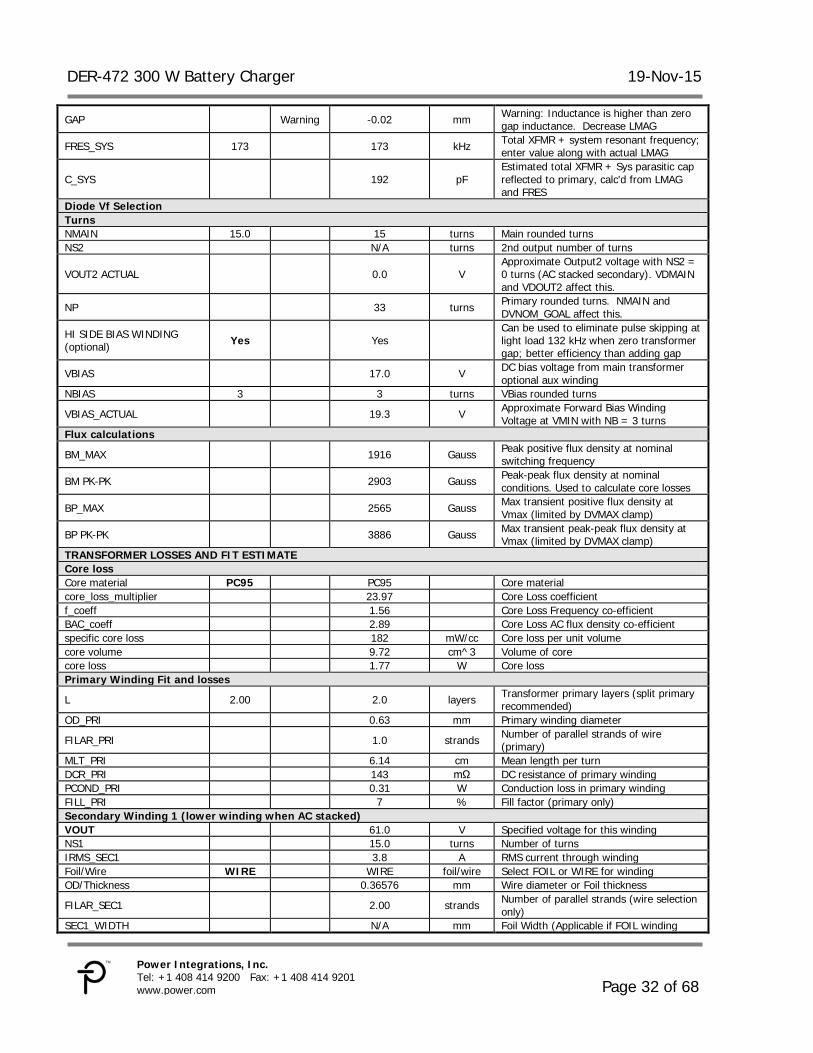
DER-472 300 W Battery Charger 19-Nov-15
Page 32 of 68
Power Integrations, Inc. Tel: +1 408 414 9200 Fax: +1 408 414 9201 www.power.com
GAP Warning -0.02 mm Warning: Inductance is higher than zero gap inductance. Decrease LMAG
FRES_SYS 173 173 kHz Total XFMR + system resonant frequency; enter value along with actual LMAG
C_SYS 192 pF Estimated total XFMR + Sys parasitic cap reflected to primary, calc'd from LMAG and FRES
Diode Vf Selection Turns NMAIN 15.0 15 turns Main rounded turns NS2 N/A turns 2nd output number of turns
VOUT2 ACTUAL 0.0 V Approximate Output2 voltage with NS2 = 0 turns (AC stacked secondary). VDMAIN and VDOUT2 affect this.
NP 33 turns Primary rounded turns. NMAIN and DVNOM_GOAL affect this.
HI SIDE BIAS WINDING (optional) Yes Yes
Can be used to eliminate pulse skipping at light load 132 kHz when zero transformer gap; better efficiency than adding gap
VBIAS 17.0 V DC bias voltage from main transformer optional aux winding
NBIAS 3 3 turns VBias rounded turns
VBIAS_ACTUAL 19.3 V Approximate Forward Bias Winding Voltage at VMIN with NB = 3 turns
Flux calculations
BM_MAX 1916 Gauss Peak positive flux density at nominal switching frequency
BM PK-PK 2903 Gauss Peak-peak flux density at nominal conditions. Used to calculate core losses
BP_MAX 2565 Gauss Max transient positive flux density at Vmax (limited by DVMAX clamp)
BP PK-PK 3886 Gauss Max transient peak-peak flux density at Vmax (limited by DVMAX clamp)
TRANSFORMER LOSSES AND FIT ESTIMATE Core loss Core material PC95 PC95 Core material core_loss_multiplier 23.97 Core Loss coefficient f_coeff 1.56 Core Loss Frequency co-efficient BAC_coeff 2.89 Core Loss AC flux density co-efficient specific core loss 182 mW/cc Core loss per unit volume core volume 9.72 cm^3 Volume of core core loss 1.77 W Core loss Primary Winding Fit and losses
L 2.00 2.0 layers Transformer primary layers (split primary recommended)
OD_PRI 0.63 mm Primary winding diameter
FILAR_PRI 1.0 strands Number of parallel strands of wire (primary)
MLT_PRI 6.14 cm Mean length per turn DCR_PRI 143 mΩ DC resistance of primary winding PCOND_PRI 0.31 W Conduction loss in primary winding FILL_PRI 7 % Fill factor (primary only) Secondary Winding 1 (lower winding when AC stacked) VOUT 61.0 V Specified voltage for this winding NS1 15.0 turns Number of turns IRMS_SEC1 3.8 A RMS current through winding Foil/Wire WIRE WIRE foil/wire Select FOIL or WIRE for winding OD/Thickness 0.36576 mm Wire diameter or Foil thickness
FILAR_SEC1 2.00 strands Number of parallel strands (wire selection only)
SEC1_WIDTH N/A mm Foil Width (Applicable if FOIL winding

19-Nov-15 DER-472 300 W Battery Charger
Page 33 of 68
Power Integrations Tel: +1 408 414 9200 Fax: +1 408 414 9201
www.power.com
used) SEC1_MLT 6.14 cm Mean length per turn DCR_SEC1 96.86 mΩ DC resistance of secondary winding PCOND_SEC1 1.38 W Conduction loss in secondary winding FILL_SEC1 2 % Fill factor (secondary 1 only) Secondary Winding 2 (upper winding when AC stacked) VOUT 0.0 V Specified voltage for this winding NS2 0.0 turns Number of turns IRMS_SEC2 0.0 A RMS current through winding Foil/Wire FOIL FOIL foil/wire Select FOIL or WIRE for winding OD/Thickness 0.125 mm Wire diameter or Foil thickness
FILAR_SEC2 N/A strands Number of parallel strands (wire selection only)
SEC2_WIDTH 18.0 mm Foil Width (Applicable if FOIL winding used)
SEC2_MLT 6.14 cm Mean length per turn DCR_SEC2 0.00 mΩ DC resistance of secondary winding PCOND_SEC2 0.00 W Conduction loss in secondary winding FILL_SEC2 0 % Fill factor (secondary 1 only) Fill Factor and losses of main transformer FILL_TOTAL 9 % Total transformer fill factor TOTAL_CU_LOSS 1.69 W Total copper losses in transformer TOTAL_CORE_LOSS 1.77 W Total core losses in transformer TOTAL_TRF_LOSS 3.46 W Total losses in transformer CURRENT WAVESHAPE PARAMETERS IP 2.79 A Peak primary current at Full Load, VNOM
IP_PEAK 2.79 A Peak primary current at Peak Load and VNOM
IPRMS(NOM) 1.49 A Primary RMS current at Full Load, VNOM IMAG 0.25 A Peak magnetizing current at VMIN OUTPUT INDUCTOR
KDI_ACTUAL 0.44 Current ripple factor of combined Main and Output2 outputs
Turns
POWDER TURNS MULTIPLIER 3.00 3.0
Powder only. Multiplier factor between main number of turns in transformer and inductor (default value = 3 for 66kHz or 4 for 132kHz).
NMAIN_INDUCTOR 45.0 turns Main output inductor number of turns - affected by powder turns multiplier or ferrite Target BM
NOUT2_INDUCTOR turns Output 2 inductor number of turns NOUT4_INDUCTOR N/A turns Output 4 number of turns (low power) Inductance and flux
LMAIN_ACTUAL 144.9 uH Estimated inductance of main output at full load
LOUT_2 0.0 uH Estimated inductance of auxiliary output at full load
BM_IND 2412 gauss DC component of flux density BAC_IND 498 gauss AC component of flux density Core Selection
Core Type Kool Mu 125u Kool Mu 125u Select core type
Core Auto 77930(O.D)=27.7 Output choke core size - verify on bench AE 65.4 mm^2 Core Effective Cross Sectional Area LE 63.5 mm Core Effective Path Length AL 157.0 nH/T^2 Ungapped Core Effective Inductance BW 44.3 mm Bobbin Physical Winding Width VE 4150 mm^3 Volume of core Powder cores (Sendust and Powdered Iron) Cores MUR 125 Relative permeability of material at 0 bias

DER-472 300 W Battery Charger 19-Nov-15
Page 34 of 68
Power Integrations, Inc. Tel: +1 408 414 9200 Fax: +1 408 414 9201 www.power.com
H 34.7 AT/cm Magnetic field strength
MUR_RATIO 0.46 Ratio of permeability at full load divided by initial permeability
LMAIN_0bias 317.9 uH Estimated inductance of main output with 0 DC bias
Ferrite Cores LG N/A mm Gap length of inductor cores Target BM N/A Gauss Target maximum flux density Choke wires Total number of layers 1.80 layers Total number of layers for chosen toroid
IRMS_MAIN 4.59 A RMS current through main inductor windings
IRMS_AUX 0.00 A RMS current through aux winding AWG_MAIN 20.00 20 AWG Main inductor winding wire gauge OD_MAIN 0.88 mm Main winding wire gauge outer diameter
FILAR_MAIN 2 strands Number of parallel strands for main output
RDC_MAIN 28.88 mΩ Resistance of wire for main inductor winding
AC Resistance Ratio (Main) 11.79 Ratio of total resistance (AC + DC) to the DC resistance (using Dowell curves)
CMA_MAIN 445 CMA Cir mils per amp for main inductor winding
J_MAIN 7.57 A/mm^2 Current density in main inductor winding AWG_AUX 0 AWG Aux winding wire gauge
OD_AUX N/A mm Auxiliary winding wire gauge outer diameter
FILAR_AUX 2 strands Number of parallel strands for aux output
RDC_AUX 0.00 mΩ Resistance of wire for aux inductor winding
AC Resistance Ratio (Aux) 0.00 Ratio of total resistance (AC + DC) to the DC resistance (using Dowell curves)
CMA_AUX Info 0 CMA !!! Info. Low CMA may cause overheating. Verify acceptable temperature rise
J_AUX 0.00 A/mm^2 Current density in auxiliary winding Choke Losses PCOPPER_MAIN 0.61 W Copper loss in main inductor winding PCOPPER_AUX 0.00 W Copper loss in aux inductor windings PCORE 1.28 W Total core loss PTOTAL_IND 1.89 W Total losses in output choke SECONDARY OUTPUT DIODE PARAMETERS Main Output
ISFWDRMS 3.77 A Full load forward diode RMS current at nominal input voltage
ISCATCHRMS 4.14 A Freewheeling diode RMS current at nominal input voltage
IDAVMAINF 3.07 A Worst case average current of forward rectifier at VMIN (single device rating)
IDAVMAINC 2.89 A Worst case average current of freewheeling diode at VMAX(single device rating)
IRMSMAIN 0.58 A Maximum RMS current, Main output capacitor
PD_LOSS_MAIN 2.30 W Conduction loss of forward diode Second Output
ISFWD2RMS 0.00 A Full load forward diode RMS current at nominal input voltage
ISCATCH2RMS 0.00 A Freewheeling diode RMS current at nominal input voltage
IDAVOUT2F 0.00 A Worst case average current of forward rectifier at VMIN (single device rating)

19-Nov-15 DER-472 300 W Battery Charger
Page 35 of 68
Power Integrations Tel: +1 408 414 9200 Fax: +1 408 414 9201
www.power.com
IDAVOUT2C 0.00 A Worst case average current of freewheeling diode at VMAX(single device rating)
IRMSOUT2 0.00 A Maximum RMS current, Main output capacitor
PD_LOSS_OUT2 0.00 W Conduction loss of forward diode Diode Derating
VPIVMAINF 0.80 301.1 V Main Forward Diode peak-inverse voltage (at VDSOP), including derating
VPIVMAINC 0.80 222.9 V Main Catch Diode peak-inverse voltage (at VOVOFF_MAX), including derating
VPIVOUT2F 1.00 0.0 V Output2 Forward Diode peak-inverse voltage (at VDSOP), including derating
VPIVOUT2C 1.00 0.0 V Output2 Catch Diode peak-inverse voltage (at VOVOFF_MAX), including derating
VPIVB 1.00 48.2 V Bias output rectifier peak-inverse voltage (at VDSOP), including derating
Hiper-TFS STANDBY SECTION (FLYBACK STAGE) ENTER APPLICATION VARIABLES VACMIN 85 V Minimum AC Input Voltage VACMAX 132 132 V Maximum AC Input Voltage fL 50 Hz AC Mains Frequency VO_SB 5.0 V Output Voltage (at continuous power)
IO_SB 4.00 4.00 A Power Supply Output Current (corresponding to peak power)
IO_SB_PK 4.00 A Peak output current POUT_SB 20.00 W Continuous Output Power
POUT_SB_TOTAL 20.32 W Total Standby power (Includes Bias winding power)
POUT_SB_PK 20.32 W Peak Standby Output Power
n 0.70 Efficiency Estimate at output terminals. Under 0.7 if no better data available
Z 0.50 Z Factor. Ratio of secondary side losses to the total losses in the power supply. Use 0.5 if no better data available
tC 3.00 ms Bridge Rectifier Conduction Time Estimate ENTER Hiper-TFS STANDBY VARIABLES
Select Current Limit INC Increased Current Limit
Enter "LOW" for low current limit, "RED" for reduced current limit (sealed adapters), "STD" for standard current limit or "INC" for increased current limit (peak or higher power applications)
ILIM_MIN 0.70 A Minimum Current Limit ILIM_TYP 0.75 A Typical Current Limit ILIM_MAX 0.80 A Maximum Current Limit R(EN) 107 kΩ Enable pin resistor fSmin 124,000 Hz Minimum Device Switching Frequency
I^2fmin 66.8 A^2kHz I^2f (product of current limit squared and frequency is trimmed for tighter tolerance)
VOR 100 V Reflected Output Voltage (VOR < 135 V Recommended)
VDS 10.0 V Hiper-TFS Standby On State Drain to Source Voltage
VD_SB 0.5 V Output Winding Diode Forward Voltage Drop
KP 0.51 Ripple to Peak Current Ratio (KP < 6)
KP_TRANSIENT 0.27 Transient Ripple to Peak Current Ratio. Ensure KP_TRANSIENT > 0.25
ENTER BIAS WINDING VARIABLES VB 16.0 V Bias Winding Voltage IB 20.0 mA Bias winding Load current

DER-472 300 W Battery Charger 19-Nov-15
Page 36 of 68
Power Integrations, Inc. Tel: +1 408 414 9200 Fax: +1 408 414 9201 www.power.com
PB 0.32 W Bias winding power VDB 0.70 V Bias Winding Diode Forward Voltage Drop NB 12.1 turns Bias Winding Number of Turns
VZOV 22 V Over Voltage Protection zener diode voltage.
UVLO VARIABLES
RLS 3.32 MΩ Line sense resistor (from Main converter section)
V_UV_ACTUAL 85 V Typical DC start-up voltage ENTER TRANSFORMER CORE/CONSTRUCTION VARIABLES Core Type EF25 EF25 Enter Transformer Core AE 0.518 cm^2 Core Effective Cross Sectional Area LE 5.78 cm Core Effective Path Length AL 2000 nH/T^2 Ungapped Core Effective Inductance BW 15.6 mm Bobbin Physical Winding Width
M 1.50 1.5 mm Safety Margin Width (Half the Primary to Secondary Creepage Distance)
L 2.00 2 Number of Primary Layers NS_SB 4 4 Number of Secondary Turns DC INPUT VOLTAGE PARAMETERS VMIN_SB 113 V Minimum DC Input Voltage VMAX_SB 187 V Maximum DC Input Voltage CURRENT WAVEFORM SHAPE PARAMETERS
DMAX_SB 0.49 Duty Ratio at full load, minimum primary inductance and minimum input voltage
IAVG 0.28 A Average Primary Current IP_SB 0.70 A Minimum Peak Primary Current IR_SB 0.35 A Primary Ripple Current IRMS_SB 0.43 A Primary RMS Current TRANSFORMER PRIMARY DESIGN PARAMETERS
LP_SB 1074 uH Typical Primary Inductance. +/- 10% to ensure a minimum primary inductance of 976 uH
LP_TOLERANCE 10 % Primary inductance tolerance NP_SB 73 turns Primary Winding Number of Turns ALG 203 nH/T^2 Gapped Core Effective Inductance
BM 2287 Gauss Maximum Operating Flux Density, BM<3000 is recommended
BAC 579 Gauss AC Flux Density for Core Loss Curves (0.5 X Peak to Peak)
ur 1776 Relative Permeability of Ungapped Core LG 0.29 mm Gap Length (Lg > 0.1 mm) BWE 25.2 mm Effective Bobbin Width
OD 0.35 mm Maximum Primary Wire Diameter including insulation
INS 0.06 mm Estimated Total Insulation Thickness (= 2 * film thickness)
DIA 0.29 mm Bare conductor diameter
AWG 29 AWG Primary Wire Gauge (Rounded to next smaller standard AWG value)
CM 128 Cmils Bare conductor effective area in circular mils
CMA 299 Cmils/Amp Primary Winding Current Capacity (200 < CMA < 500)
TRANSFORMER SECONDARY DESIGN PARAMETERS Lumped parameters ISP 12.7 A Peak Secondary Current ISRMS 7.91 A Secondary RMS Current IRIPPLE 6.83 A Output Capacitor RMS Ripple Current CMS 1583 Cmils Secondary Bare Conductor minimum

19-Nov-15 DER-472 300 W Battery Charger
Page 37 of 68
Power Integrations Tel: +1 408 414 9200 Fax: +1 408 414 9201
www.power.com
circular mils
AWGS 18 AWG Secondary Wire Gauge (Rounded up to next larger standard AWG value)
VOLTAGE STRESS PARAMETERS
VDRAIN 417 V Maximum Drain Voltage Estimate (Assumes 20% zener clamp tolerance and an additional 10% temperature tolerance)
PIVS 15 V Output Rectifier Maximum Peak Inverse Voltage
Forward DC-DC System efficiency P_MOSFET_MAIN_TOTAL 7.17 W HiperTFS losses P_XFMR_LOSS 3.5 W Main transformer losses P_MAIN_OUT_DIODE 2.3 W Output diode losses P_CIN_ESR 0.32 W Bulk capacitor ESR losses P_IND_MAIN 1.9 W Output choke losses
OTHER_LOSSES 0.13 W Other losses (includes PCB traces, clamp loss, magamp loss etc.)
EFFICIENCY_STDBY 70.0% Estimated efficiency of flyback power supply
EFFICIENCY_MAIN 94.6% Estimated Forward efficiency
EFFICIENCY_SYSTEM 92.4% Estimated System efficiency (forward + standby)
Other Losses Detailed Mosfet Loss Information

DER-472 300 W Battery Charger 19-Nov-15
Page 38 of 68
Power Integrations, Inc. Tel: +1 408 414 9200 Fax: +1 408 414 9201 www.power.com
9 Heat Sinks
9.1 Main Primary Heat Sink
Primary Heat Sink Sheet Metal 9.1.1
Figure 11 – DER-472 Primary Heat Sink Sheet Metal Drawing.
19-Nov-15 DER-472 300 W Battery Charger
Page 39 of 68
Power Integrations Tel: +1 408 414 9200 Fax: +1 408 414 9201
www.power.com
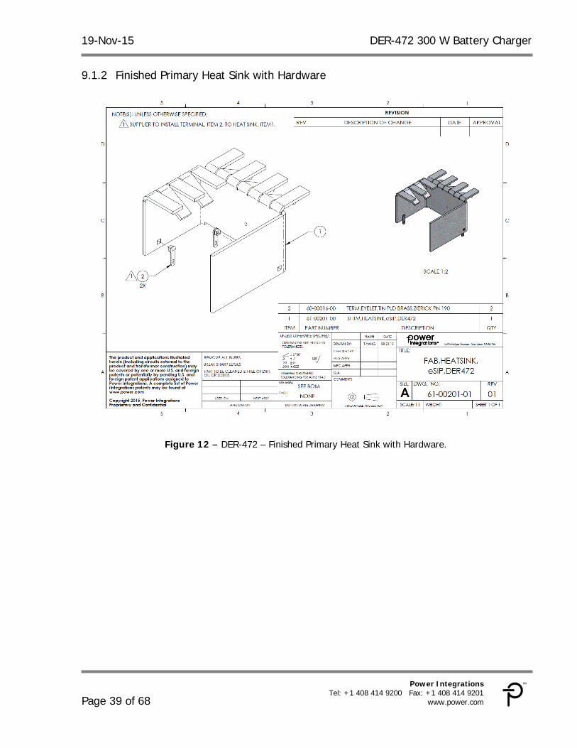
Finished Primary Heat Sink with Hardware 9.1.2
Figure 12 – DER-472 – Finished Primary Heat Sink with Hardware.

DER-472 300 W Battery Charger 19-Nov-15
Page 40 of 68
Power Integrations, Inc. Tel: +1 408 414 9200 Fax: +1 408 414 9201 www.power.com
Primary Heat Sink Assembly 9.1.3
Figure 13 – Primary Heat Sink Assembly

19-Nov-15 DER-472 300 W Battery Charger
Page 41 of 68
Power Integrations Tel: +1 408 414 9200 Fax: +1 408 414 9201
www.power.com
9.2 Diode Bridge Heat Sink
Diode Bridge Heat Sink Sheet Metal 9.2.1
Figure 14 – DER-472 Diode Bridge Heat Sink Sheet Metal Drawing.

DER-472 300 W Battery Charger 19-Nov-15
Page 42 of 68
Power Integrations, Inc. Tel: +1 408 414 9200 Fax: +1 408 414 9201 www.power.com
Completed Diode Bridge Heat Sink with Hardware 9.2.2
Figure 15 – DER-472 Finished Diode Bridge Heat Sink with Hardware.

19-Nov-15 DER-472 300 W Battery Charger
Page 43 of 68
Power Integrations Tel: +1 408 414 9200 Fax: +1 408 414 9201
www.power.com
Diode Bridge Heat Sink Assembly 9.2.3
Figure 16 – DER-472 Diode Bridge Heat Sink Assembly.

DER-472 300 W Battery Charger 19-Nov-15
Page 44 of 68
Power Integrations, Inc. Tel: +1 408 414 9200 Fax: +1 408 414 9201 www.power.com
9.3 Output Rectifier Heat Sink
Output Rectifier Heat Sink Sheet Metal Drawing 9.3.1
Figure 17 – DER-472 Output Rectifier Heat Sink Sheet Metal Drawing.
19-Nov-15 DER-472 300 W Battery Charger
Page 45 of 68
Power Integrations Tel: +1 408 414 9200 Fax: +1 408 414 9201
www.power.com
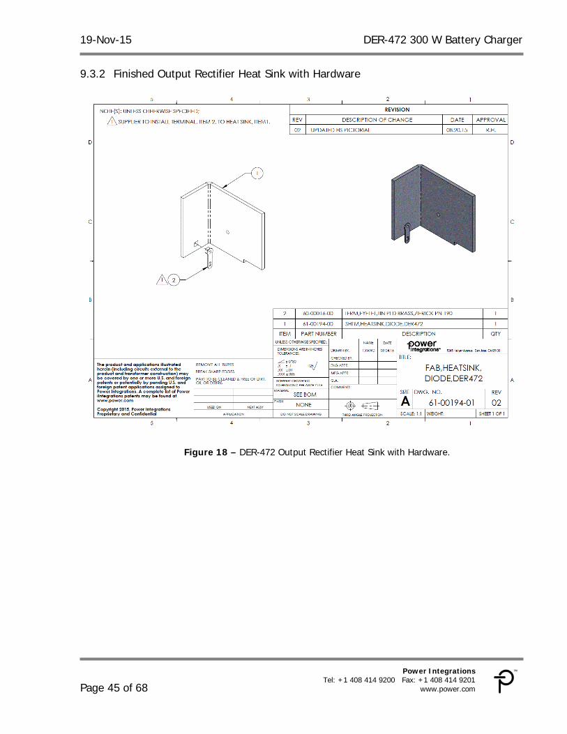
Finished Output Rectifier Heat Sink with Hardware 9.3.2
Figure 18 – DER-472 Output Rectifier Heat Sink with Hardware.
DER-472 300 W Battery Charger 19-Nov-15
Page 46 of 68
Power Integrations, Inc. Tel: +1 408 414 9200 Fax: +1 408 414 9201 www.power.com
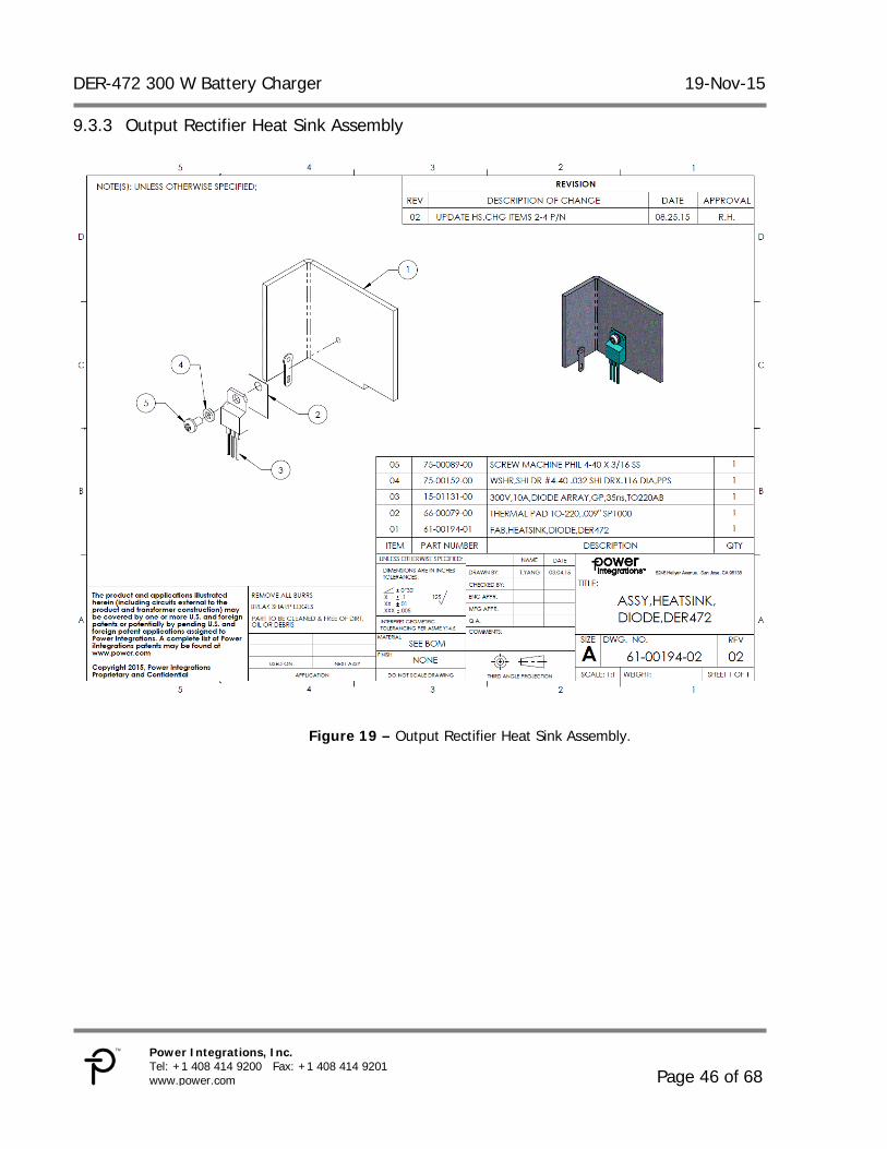
Output Rectifier Heat Sink Assembly 9.3.3
Figure 19 – Output Rectifier Heat Sink Assembly.
19-Nov-15 DER-472 300 W Battery Charger
Page 47 of 68
Power Integrations Tel: +1 408 414 9200 Fax: +1 408 414 9201
www.power.com
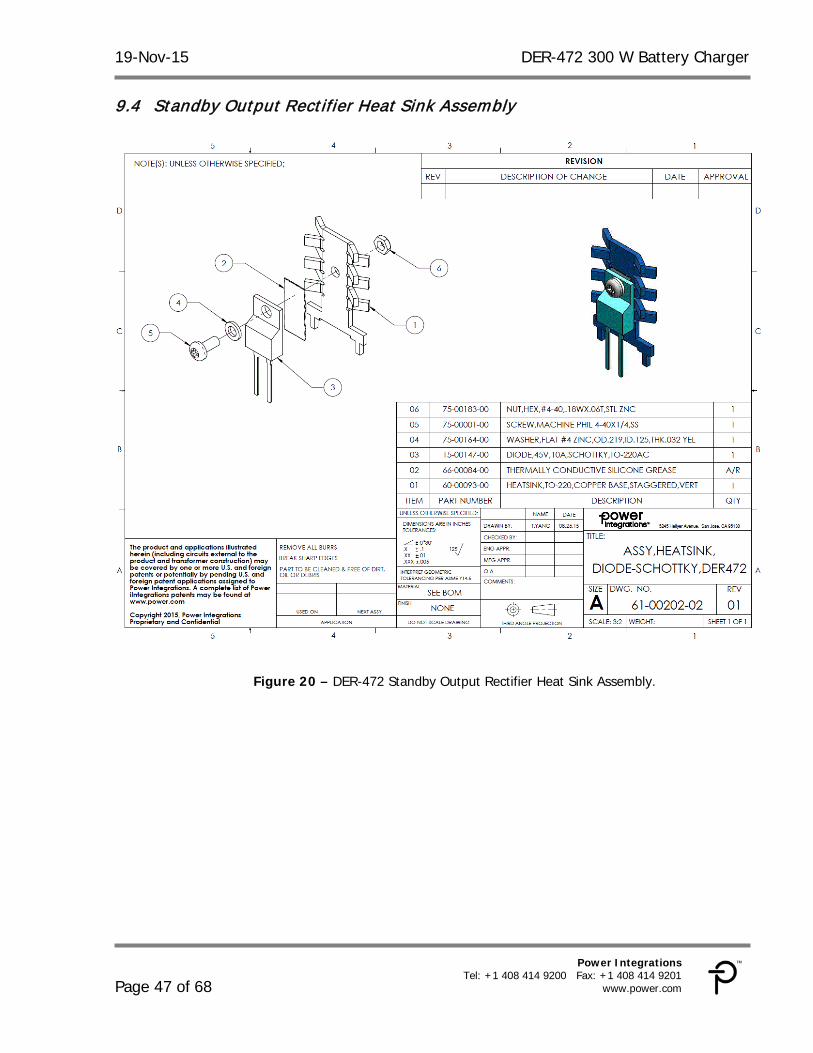
9.4 Standby Output Rectifier Heat Sink Assembly
Figure 20 – DER-472 Standby Output Rectifier Heat Sink Assembly.
DER-472 300 W Battery Charger 19-Nov-15
Page 48 of 68
Power Integrations, Inc. Tel: +1 408 414 9200 Fax: +1 408 414 9201 www.power.com
10 Performance Data All measurements were taken at room temperature and 60 Hz (input frequency) unless otherwise specified. Output voltage measurements were taken at the output connectors.
10.1 Output Load Considerations for Testing a CV/ CC Supply in Battery Charger Applications Since this power supply has a constant voltage/constant current output and normally operates in CC mode in its intended application (battery charging), some care must be taken in selecting the type/s of output load for testing. The default setting for most electronic loads is constant current. This setting can be used in testing a CV/CC supply in the CV portion of its load range below the power supply current limit set point. Once the current limit of the DUT is reached, a constant current load will cause the output voltage of the DUT to immediately collapse to the minimum voltage capability of the electronic load. To test a CV/CC supply in both its CV and CC regions (an example - obtaining a V-I characteristic curve that spans both the CV and CC regions of operation), an electronic load set for constant resistance can be used. However, in an application where the control loop is strongly affected by the output impedance, use of a CR load will give results for loop compensation that are overly optimistic and will likely oscillate when tested with an actual low impedance battery load. For final characterization and tuning the output control loops, a constant voltage load should be used. Having said this, many electronic loads incorporate a constant voltage setting, but the output impedance of the load in this setting may not be sufficiently low to successfully emulate a real-world battery (impedance on the order of tens of milliohms). Simulating this impedance can be crucial in properly setting the compensation of the current control loop in order to prevent oscillation in a real-life application.
19-Nov-15 DER-472 300 W Battery Charger
Page 49 of 68
Power Integrations Tel: +1 408 414 9200 Fax: +1 408 414 9201
www.power.com
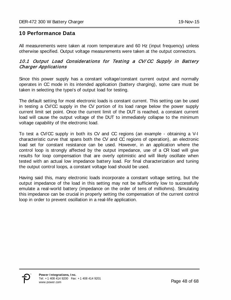
10.2 Efficiency To make this measurement, the supply was powered with an AC source. The figure shown includes the efficiency of the main forward stage combined with that of the standby/bias flyback supply.
Figure 21 – Efficiency vs. Output Power, 115 VAC Input.
72
74
76
78
80
82
84
86
88
90
92
0 25 50 75 100 125 150 175 200 225 250 275 300 325
Effi
cien
cy (
%)
Output Power (W)

DER-472 300 W Battery Charger 19-Nov-15
Page 50 of 68
Power Integrations, Inc. Tel: +1 408 414 9200 Fax: +1 408 414 9201 www.power.com
10.3 No-Load Input Power No-load input power was measured with no-load on the main and standby outputs and with the main enable switch turned off, such that only the standby supply remained active.
Figure 22 – No-Load Input Power vs. Input Voltage.
100
120
140
160
180
200
220
240
260
280
300
80 85 90 95 100 105 110 115 120 125 130 135 140
Inpu
t P
ower
(m
W)
Input Voltage (VAC)
19-Nov-15 DER-472 300 W Battery Charger
Page 51 of 68
Power Integrations Tel: +1 408 414 9200 Fax: +1 408 414 9201
www.power.com
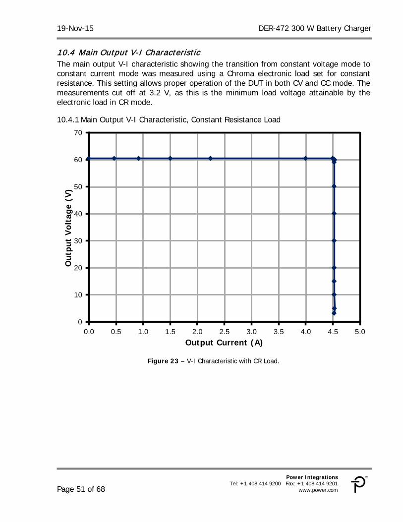
10.4 Main Output V-I Characteristic The main output V-I characteristic showing the transition from constant voltage mode to constant current mode was measured using a Chroma electronic load set for constant resistance. This setting allows proper operation of the DUT in both CV and CC mode. The measurements cut off at 3.2 V, as this is the minimum load voltage attainable by the electronic load in CR mode.
Main Output V-I Characteristic, Constant Resistance Load 10.4.1
Figure 23 – V-I Characteristic with CR Load.
0
10
20
30
40
50
60
70
0.0 0.5 1.0 1.5 2.0 2.5 3.0 3.5 4.0 4.5 5.0
Out
put
Vol
tage
(V
)
Output Current (A)

DER-472 300 W Battery Charger 19-Nov-15
Page 52 of 68
Power Integrations, Inc. Tel: +1 408 414 9200 Fax: +1 408 414 9201 www.power.com
Main Output V-I Characteristic, Constant Voltage Load 10.4.2The main output V-I characteristic in constant current mode was measured using a Chroma electronic load set for constant voltage mode. The minimum operating voltage of the load in CV mode is ~0.37 V.
Figure 24 – V-I Characteristic with CV Load.
0
10
20
30
40
50
60
70
0 1 2 3 4 5 6 7 8 9
Out
put
Vol
tage
(V
)
Output Current (A)
19-Nov-15 DER-472 300 W Battery Charger
Page 53 of 68
Power Integrations Tel: +1 408 414 9200 Fax: +1 408 414 9201
www.power.com
11 Waveforms
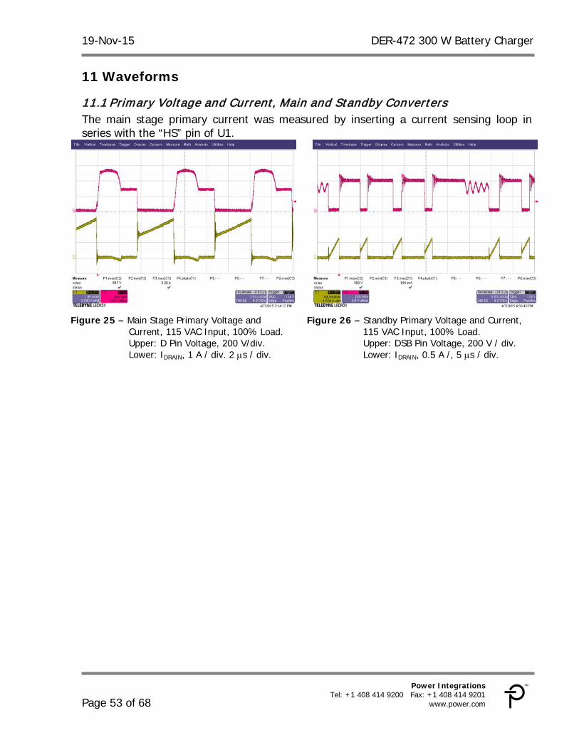
11.1 Primary Voltage and Current, Main and Standby Converters The main stage primary current was measured by inserting a current sensing loop in series with the “HS” pin of U1.
Figure 25 – Main Stage Primary Voltage and Current, 115 VAC Input, 100% Load. Upper: D Pin Voltage, 200 V/div. Lower: IDRAIN, 1 A / div. 2 µs / div.
Figure 26 – Standby Primary Voltage and Current, 115 VAC Input, 100% Load. Upper: DSB Pin Voltage, 200 V / div. Lower: IDRAIN, 0.5 A /, 5 µs / div.
DER-472 300 W Battery Charger 19-Nov-15
Page 54 of 68
Power Integrations, Inc. Tel: +1 408 414 9200 Fax: +1 408 414 9201 www.power.com
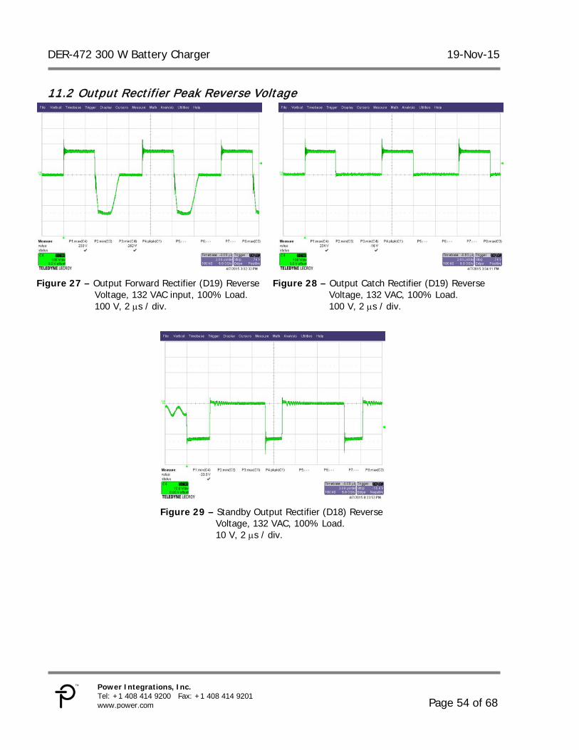
11.2 Output Rectifier Peak Reverse Voltage
Figure 27 – Output Forward Rectifier (D19) Reverse Voltage, 132 VAC input, 100% Load. 100 V, 2 µs / div.
Figure 28 – Output Catch Rectifier (D19) Reverse Voltage, 132 VAC, 100% Load. 100 V, 2 µs / div.
Figure 29 – Standby Output Rectifier (D18) Reverse
Voltage, 132 VAC, 100% Load. 10 V, 2 µs / div.
19-Nov-15 DER-472 300 W Battery Charger
Page 55 of 68
Power Integrations Tel: +1 408 414 9200 Fax: +1 408 414 9201
www.power.com
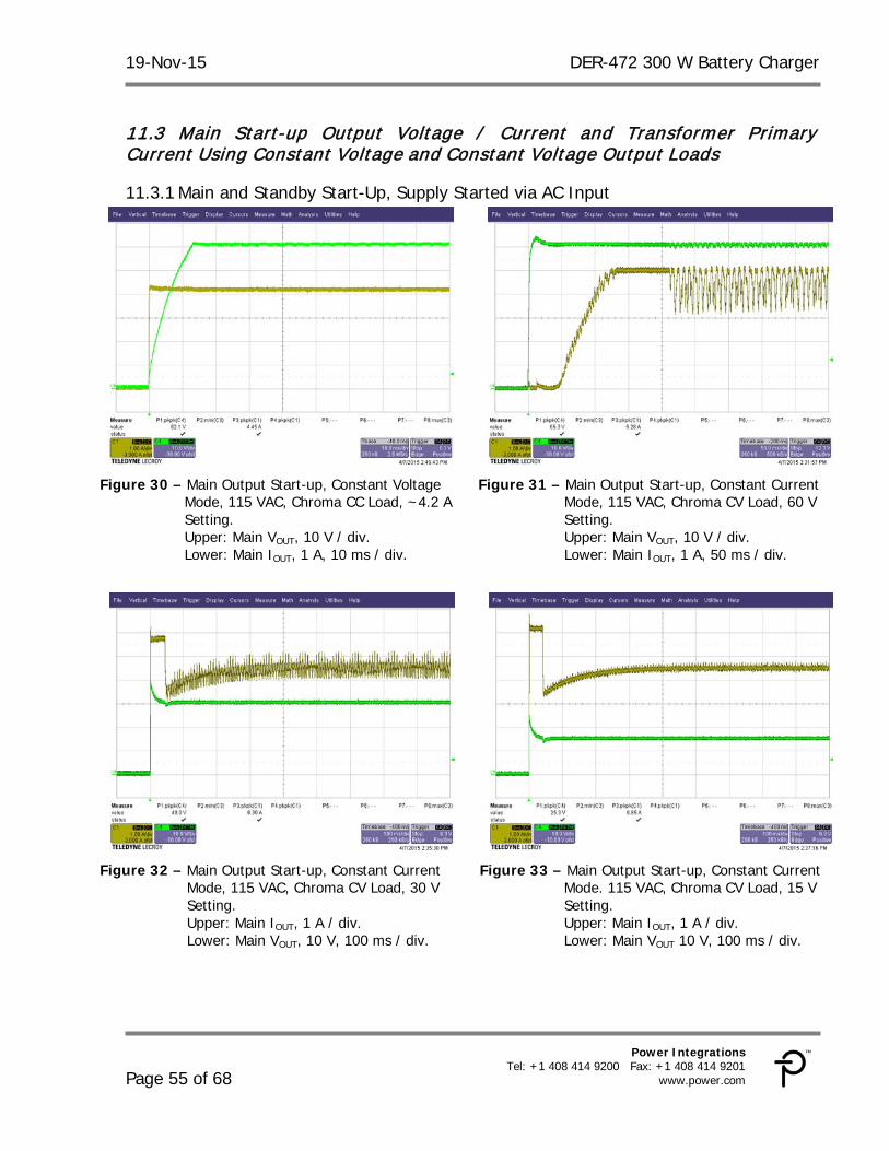
11.3 Main Start-up Output Voltage / Current and Transformer Primary Current Using Constant Voltage and Constant Voltage Output Loads
Main and Standby Start-Up, Supply Started via AC Input 11.3.1
Figure 30 – Main Output Start-up, Constant Voltage Mode, 115 VAC, Chroma CC Load, ~4.2 A Setting. Upper: Main VOUT, 10 V / div. Lower: Main IOUT, 1 A, 10 ms / div.
Figure 31 – Main Output Start-up, Constant Current Mode, 115 VAC, Chroma CV Load, 60 V Setting. Upper: Main VOUT, 10 V / div. Lower: Main IOUT, 1 A, 50 ms / div.
Figure 32 – Main Output Start-up, Constant Current Mode, 115 VAC, Chroma CV Load, 30 V Setting. Upper: Main IOUT, 1 A / div. Lower: Main VOUT, 10 V, 100 ms / div.
Figure 33 – Main Output Start-up, Constant Current Mode. 115 VAC, Chroma CV Load, 15 V Setting. Upper: Main IOUT, 1 A / div. Lower: Main VOUT 10 V, 100 ms / div.

DER-472 300 W Battery Charger 19-Nov-15
Page 56 of 68
Power Integrations, Inc. Tel: +1 408 414 9200 Fax: +1 408 414 9201 www.power.com
Figure 34 – Standby Start-up, 100% Load,
115 VAC Input, 1 V / 5 ms / div. Figure 35 – Standby Start-up, No-Load,
115 VAC Input, 1 V / 5 ms / div.
Main Output Start-Up Using Enable Switch 11.3.2
Figure 36 – Main Output Start-up, Constant Voltage
Mode, 115 VAC, Chroma CC Load, ~4.2 A Setting. Upper: Main VOUT, 10 V / div. Lower: Main IOUT, 1 A, 10 ms / div.
Figure 37 – Main Output Start-up, Constant Current Mode, 115 VAC, Chroma CV Load, 60 V Setting. Upper: Main VOUT, 10 V / div. Lower: Main IOUT, 1 A, 100 ms / div.

19-Nov-15 DER-472 300 W Battery Charger
Page 57 of 68
Power Integrations Tel: +1 408 414 9200 Fax: +1 408 414 9201
www.power.com
Figure 38 – Main Output Start-up, Constant Current
Mode, 115 VAC, Chroma CV Load, 30 V Setting. Upper: Main IOUT, 1 A / div. Lower: Main VOUT, 10 V, 100 ms / div.
Figure 39 – Main Output Start-up, Constant Current Mode, 115 VAC, Chroma CV Load, 15 V Setting. Upper: Main IOUT, 1 A / div. Lower: Main VOUT 10 V, 100 ms / div.
11.4 Load Transient Response, Voltage Mode 50% -75% -50% Load Step 32 cycles of averaging were used on load transient waveforms to filter out ripple and better view actual output voltage excursion due to load transient.
Figure 40 – Main Output Transient Response, CV Mode,
50%-75%-50% Load Step, 115 VAC Input. Upper: VOUT, 200 mV / div. Lower: Main Output ILOAD, 1 A, 500 µs / div.
Figure 41 – Standby Output Transient Response, CV Mode, 50%-75%-50% Load Step, 115 VAC Input. Upper: VOUT, 50 mV / div. Lower: Main Output ILOAD, 1 A, 500 µs / div.
DER-472 300 W Battery Charger 19-Nov-15
Page 58 of 68
Power Integrations, Inc. Tel: +1 408 414 9200 Fax: +1 408 414 9201 www.power.com
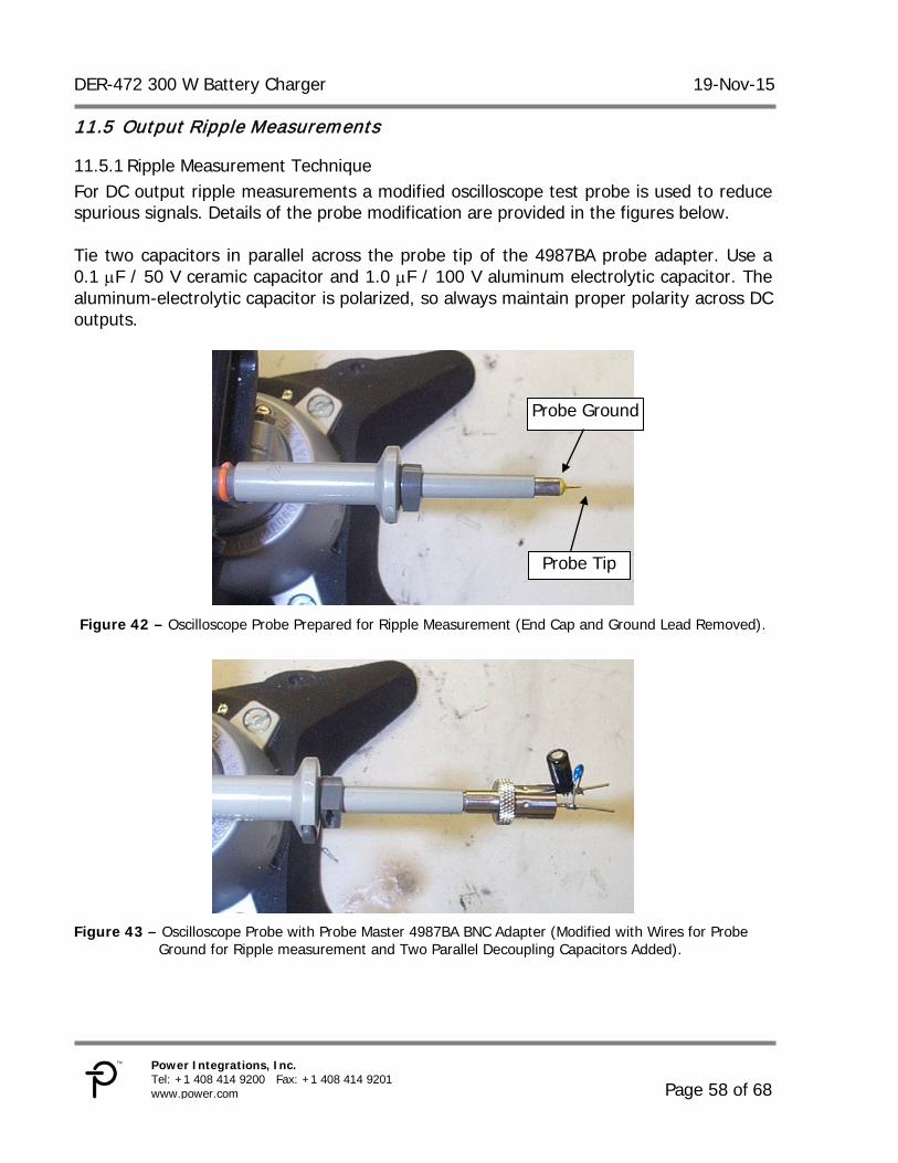
11.5 Output R ipple Measurements
Ripple Measurement Technique 11.5.1For DC output ripple measurements a modified oscilloscope test probe is used to reduce spurious signals. Details of the probe modification are provided in the figures below. Tie two capacitors in parallel across the probe tip of the 4987BA probe adapter. Use a 0.1 µF / 50 V ceramic capacitor and 1.0 µF / 100 V aluminum electrolytic capacitor. The aluminum-electrolytic capacitor is polarized, so always maintain proper polarity across DC outputs.
Figure 42 – Oscilloscope Probe Prepared for Ripple Measurement (End Cap and Ground Lead Removed).
Figure 43 – Oscilloscope Probe with Probe Master 4987BA BNC Adapter (Modified with Wires for Probe
Ground for Ripple measurement and Two Parallel Decoupling Capacitors Added).
Probe Ground
Probe Tip
19-Nov-15 DER-472 300 W Battery Charger
Page 59 of 68
Power Integrations Tel: +1 408 414 9200 Fax: +1 408 414 9201
www.power.com
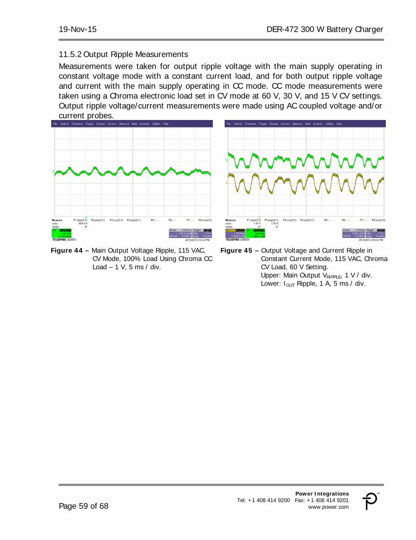
Output Ripple Measurements 11.5.2Measurements were taken for output ripple voltage with the main supply operating in constant voltage mode with a constant current load, and for both output ripple voltage and current with the main supply operating in CC mode. CC mode measurements were taken using a Chroma electronic load set in CV mode at 60 V, 30 V, and 15 V CV settings. Output ripple voltage/current measurements were made using AC coupled voltage and/or current probes.
Figure 44 – Main Output Voltage Ripple, 115 VAC, CV Mode, 100% Load Using Chroma CC Load – 1 V, 5 ms / div.
Figure 45 – Output Voltage and Current Ripple in Constant Current Mode, 115 VAC, Chroma CV Load, 60 V Setting. Upper: Main Output VRIPPLE, 1 V / div. Lower: IOUT Ripple, 1 A, 5 ms / div.

DER-472 300 W Battery Charger 19-Nov-15
Page 60 of 68
Power Integrations, Inc. Tel: +1 408 414 9200 Fax: +1 408 414 9201 www.power.com
Figure 46 – Main Output Voltage and Current Ripple in Constant Current Mode, 115 VAC, Chroma CV Load, 30 V Setting. Upper: Main Output VRIPPLE, 1 V / div. Lower:, IOUT Ripple, 1 A, 5 ms /div.
Figure 47 – Main Output Voltage and Current Ripple in Constant Current Mode, 115 VAC, Chroma CV Load, 15 V Setting. Upper: Main Output VRIPPLE, 1 V / div. Lower: IOUT Ripple, 1 A, 5 ms /div.
Figure 48 – Standby Output Voltage Ripple, 100%
Load, 115 VAC with 100% Load on Main Output – 50 mV, 5 ms / div.
Figure 49 – Standby Output Voltage Ripple, 100% Load, 115 VAC, Main Output Disabled with ON/OFF Switch – 50 mV, 5 ms / div.

19-Nov-15 DER-472 300 W Battery Charger
Page 61 of 68
Power Integrations Tel: +1 408 414 9200 Fax: +1 408 414 9201
www.power.com
12 Temperature Profiles The board was operated at room temperature, with output set at maximum using a Chroma electronic load with constant resistance for the main output and constant current mode for the standby output. The constant resistance load for the main output allows the main load to be set for maximum power output without having the main output drift into current limit and collapsing the output voltage, as can happen when a constant current load is used. The unit was allowed to thermally stabilize (~1 hr) before measurements were made.
12.1 Spot Temperature Measurements
Position Temperature (°C) 115 VAC
T1 (Main) 80.4 Outside / 95.7 (Inner Hot Spot) T2 (SBY) 62.5
BR1 65 L6 (CM) 49 L8 (CM) 49.4
L3 (Main) 55.7 R47 (Main Sec Snubber) 65.1
U1 92.9 D19 Main (FWD/CTH) 84.4
D18 SBY Rect 75 Ambient 25
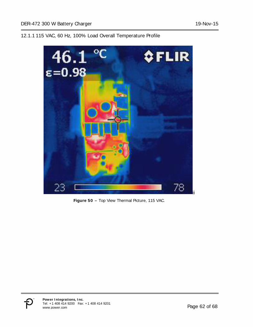
DER-472 300 W Battery Charger 19-Nov-15
Page 62 of 68
Power Integrations, Inc. Tel: +1 408 414 9200 Fax: +1 408 414 9201 www.power.com
115 VAC, 60 Hz, 100% Load Overall Temperature Profile 12.1.1
ii Figure 50 – Top View Thermal Picture, 115 VAC.
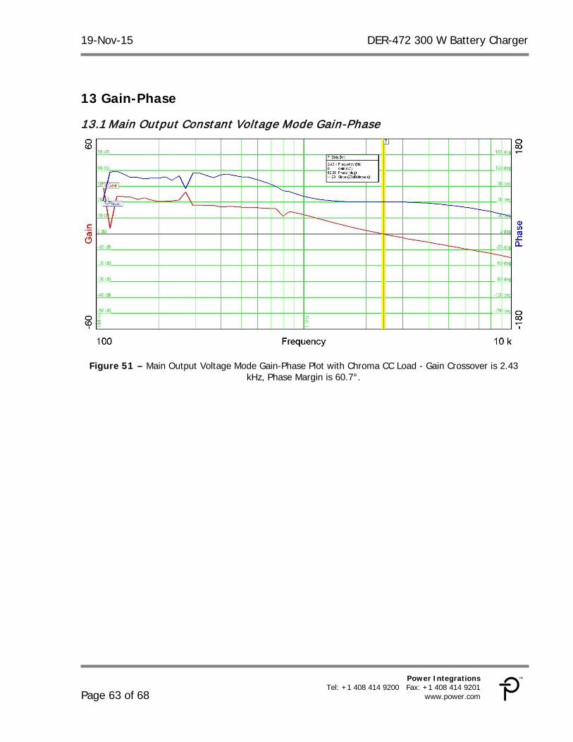
19-Nov-15 DER-472 300 W Battery Charger
Page 63 of 68
Power Integrations Tel: +1 408 414 9200 Fax: +1 408 414 9201
www.power.com
13 Gain-Phase
13.1 Main Output Constant Voltage Mode Gain-Phase
Figure 51 – Main Output Voltage Mode Gain-Phase Plot with Chroma CC Load - Gain Crossover is 2.43
kHz, Phase Margin is 60.7°.

DER-472 300 W Battery Charger 19-Nov-15
Page 64 of 68
Power Integrations, Inc. Tel: +1 408 414 9200 Fax: +1 408 414 9201 www.power.com
13.2 Main Output Constant Current Mode Gain-Phase Gain-phase was tested using a Chroma electronic load set to constant voltage mode at three set points - 60 V, 30 V, and 15 V, obtaining the gain-phase measurements for three widely separated points on the V-I characteristic curve. Using a CV load maximizes the CC loop gain (worst case for control loop) and simulates operating while charging a low impedance load like a battery. Using the constant resistance setting for the electronic load will yield overly optimistic results for gain-phase measurements and for determining component values for frequency compensation.
Figure 52 – Main Output Gain-Phase, Constant Current Output, Chroma Constant Voltage Load.
Red/Blue – 60 V Gain and Phase Crossover Frequency – 361 Hz, Phase Margin – 93°. Brown/Green – 30 V Gain and Phase Crossover Frequency – 709 Hz, Phase Margin – 79°. Pink/Purple – 15 V Gain and Phase Crossover Frequency – 668 Hz, Phase Margin – 69°.
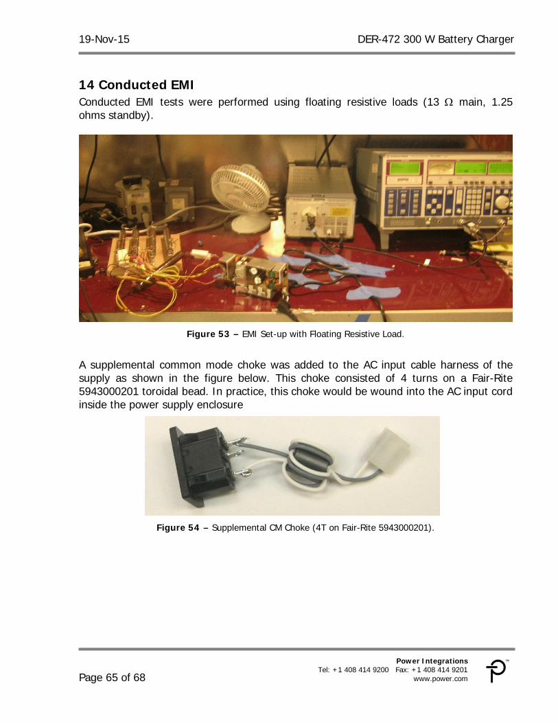
19-Nov-15 DER-472 300 W Battery Charger
Page 65 of 68
Power Integrations Tel: +1 408 414 9200 Fax: +1 408 414 9201
www.power.com
14 Conducted EMI Conducted EMI tests were performed using floating resistive loads (13 Ω main, 1.25 ohms standby).
Figure 53 – EMI Set-up with Floating Resistive Load.
A supplemental common mode choke was added to the AC input cable harness of the supply as shown in the figure below. This choke consisted of 4 turns on a Fair-Rite 5943000201 toroidal bead. In practice, this choke would be wound into the AC input cord inside the power supply enclosure
Figure 54 – Supplemental CM Choke (4T on Fair-Rite 5943000201).
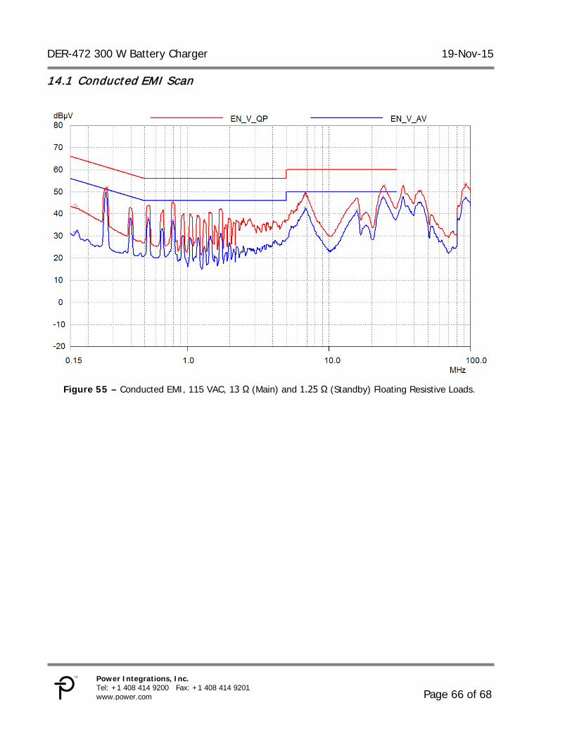
DER-472 300 W Battery Charger 19-Nov-15
Page 66 of 68
Power Integrations, Inc. Tel: +1 408 414 9200 Fax: +1 408 414 9201 www.power.com
14.1 Conducted EMI Scan
Figure 55 – Conducted EMI, 115 VAC, 13 Ω (Main) and 1.25 Ω (Standby) Floating Resistive Loads.

19-Nov-15 DER-472 300 W Battery Charger
Page 67 of 68
Power Integrations Tel: +1 408 414 9200 Fax: +1 408 414 9201
www.power.com
15 Revision History Date Author Revision Description & changes Reviewed 30-Oct-15 RH 1.0 Initial Release. Apps & Mktg 12-Nov-15 RH 1.1 Updated Circuit Description Text. 19-Nov-15 RH 1.2 Updated Circuit Description Text.

DER-472 300 W Battery Charger 19-Nov-15
Page 68 of 68
Power Integrations, Inc. Tel: +1 408 414 9200 Fax: +1 408 414 9201 www.power.com
For the latest updates, visit our website: www.power.com
Power Integrations reserves the right to make changes to its products at any time to improve reliability or manufacturability. Power Integrations does not assume any liability arising from the use of any device or circuit described herein. POWER INTEGRATIONS MAKES NO WARRANTY HEREIN AND SPECIFICALLY DISCLAIMS ALL WARRANTIES INCLUDING, WITHOUT LIMITATION, THE IMPLIED WARRANTIES OF MERCHANTABILITY, FITNESS FOR A PARTICULAR PURPOSE, AND NON-INFRINGEMENT OF THIRD PARTY RIGHTS.
Patent Information The products and applications illustrated herein (including transformer construction and circuits’ external to the products) may be covered by one or more U.S. and foreign patents, or potentially by pending U.S. and foreign patent applications assigned to Power Integrations. A complete list of Power Integrations’ patents may be found at www.power.com. Power Integrations grants its customers a license under certain patent rights as set forth at http://www.power.com/ip.htm.
The PI Logo, TOPSwitch, TinySwitch, LinkSwitch, LYTSwitch, InnoSwtich, DPA-Switch, PeakSwitch, CAPZero, SENZero, LinkZero, HiperPFS, HiperTFS, HiperLCS, Qspeed, EcoSmart, Clampless, E-Shield, Filterfuse, FluxLink, StackFET, PI Expert and PI FACTS are trademarks of Power Integrations, Inc. Other trademarks are property of their respective companies. ©Copyright 2015 Power Integrations, Inc.
Power Integrations Worldwide Sales Support Locations
WORLD HEADQUARTERS 5245 Hellyer Avenue San Jose, CA 95138, USA. Main: +1-408-414-9200 Customer Service: Phone: +1-408-414-9665 Fax: +1-408-414-9765 e-mail: [email protected]
GERMANY Lindwurmstrasse 114 80337, Munich Germany Phone: +49-895-527-39110 Fax: +49-895-527-39200 e-mail: [email protected]
JAPAN Kosei Dai-3 Building 2-12-11, Shin-Yokohama, Kohoku-ku, Yokohama-shi, Kanagawa 222-0033 Japan Phone: +81-45-471-1021 Fax: +81-45-471-3717 e-mail: [email protected]
TAIWAN 5F, No. 318, Nei Hu Rd., Sec. 1 Nei Hu District Taipei 11493, Taiwan R.O.C. Phone: +886-2-2659-4570 Fax: +886-2-2659-4550 e-mail: [email protected]
CHINA (SHANGHAI) Rm 2410, Charity Plaza, No. 88, North Caoxi Road, Shanghai, PRC 200030 Phone: +86-21-6354-6323 Fax: +86-21-6354-6325 e-mail: [email protected]
INDIA #1, 14th Main Road Vasanthanagar Bangalore-560052 India Phone: +91-80-4113-8020 Fax: +91-80-4113-8023 e-mail: [email protected]
KOREA RM 602, 6FL Korea City Air Terminal B/D, 159-6 Samsung-Dong, Kangnam-Gu, Seoul, 135-728 Korea Phone: +82-2-2016-6610 Fax: +82-2-2016-6630 e-mail: [email protected]
UK Cambridge Semiconductor, a Power Integrations company Westbrook Centre, Block 5, 2nd Floor Milton Road Cambridge CB4 1YG Phone: +44 (0) 1223-446483 e-mail: [email protected]
CHINA (SHENZHEN) 17/F, Hivac Building, No. 2, Keji Nan 8th Road, Nanshan District, Shenzhen, China, 518057 Phone: +86-755-8672-8689 Fax: +86-755-8672-8690 e-mail: [email protected]
ITALY Via Milanese 20, 3rd. Fl. 20099 Sesto San Giovanni (MI) Italy Phone: +39-024-550-8701 Fax: +39-028-928-6009 e-mail: [email protected]
SINGAPORE 51 Newton Road, #19-01/05 Goldhill Plaza Singapore, 308900 Phone: +65-6358-2160 Fax: +65-6358-2015 e-mail: [email protected]