Embed Size (px)
Citation preview
Rev.1A 18 August 2006 RD#0618 Page 1 of 24 WORLD HEADQUARTERS: 233 Kansas St., El Segundo, California 90245 Tel: (310) 252-7105
http://www.irf.com/ Data and specifications subject to change without notice.
10 Ang Mo Kio Street 65, #03-18 TechPoint, Singapore 569059
Reference Design # 0618
IRAC1166-100W
+16V Low-side Smart Rectification 100W Flyback Demo Board
User’s Guide
by
ISRAEL SERRANO
18 August 2006
Rev.1A 18 August 2006 RD#0618 Page 2 of 24 WORLD HEADQUARTERS: 233 Kansas St., El Segundo, California 90245 Tel: (310) 252-7105
http://www.irf.com/ Data and specifications subject to change without notice.
Page(s)Table of Contents 2 1.0 INTRODUCTION 3 2.0 GENERAL DESCRIPTION 3 2.1 IRAC1166-100W +16V Demo Board Schematic Diagram 4 2.2 IRAC1166-100W +16V Demo Board Pictures 5 2.3 IRAC1166-100W +16V Demo Board PCB Layout 6 3.0 Circuit Description 7 4.0 Test Connection and Set up Pictures 8 5.0 Circuit Features 9 5.1 OVT Setting 9 5.2 ENABLE Setting 9 5.3 MOT Setting 9 5.4 Mosfet Selection Design Tips 10 6.0 Test Waveforms 11-18 6.1.1 Transient Load Test 11-13 6.1.2 Static Load Test 14-15 6.1.3 Ripple And Noise Measurement 16 6.1.4 Dynamic load Test 17 6.4 Startup & UVLO Test 18 7.0 Line / Load Regulation Test 19 7.1 IR1166 Demo Board V-I Characteristics Curve 19 7.2 System Efficiency Test 20 7.3 Thermal Verification 20 8.0 Summary 21 9.0 Appendix 21-25 9.1 Transformer turns ratio, Duty Cycle and Secondary Current Relationship Chart
21
9.2 IR1166 100W +16V SR Demo Board Power Transformer Specs 22 10.0 IRAC1166-100W +16V Demo Board Bill of Materials (BOM) 23-24
Rev.1A 18 August 2006 RD#0618 Page 3 of 24 WORLD HEADQUARTERS: 233 Kansas St., El Segundo, California 90245 Tel: (310) 252-7105
http://www.irf.com/ Data and specifications subject to change without notice.
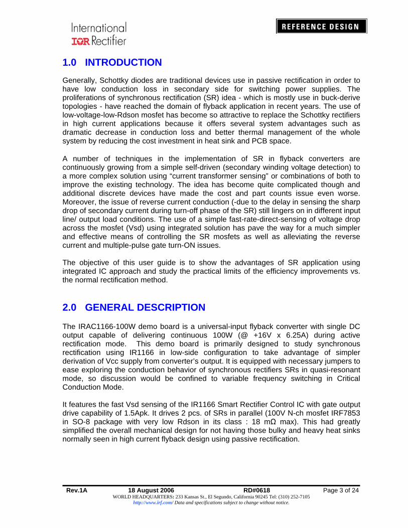
1.0 INTRODUCTION Generally, Schottky diodes are traditional devices use in passive rectification in order to have low conduction loss in secondary side for switching power supplies. The proliferations of synchronous rectification (SR) idea - which is mostly use in buck-derive topologies - have reached the domain of flyback application in recent years. The use of low-voltage-low-Rdson mosfet has become so attractive to replace the Schottky rectifiers in high current applications because it offers several system advantages such as dramatic decrease in conduction loss and better thermal management of the whole system by reducing the cost investment in heat sink and PCB space. A number of techniques in the implementation of SR in flyback converters are continuously growing from a simple self-driven (secondary winding voltage detection) to a more complex solution using “current transformer sensing” or combinations of both to improve the existing technology. The idea has become quite complicated though and additional discrete devices have made the cost and part counts issue even worse. Moreover, the issue of reverse current conduction (-due to the delay in sensing the sharp drop of secondary current during turn-off phase of the SR) still lingers on in different input line/ output load conditions. The use of a simple fast-rate-direct-sensing of voltage drop across the mosfet (Vsd) using integrated solution has pave the way for a much simpler and effective means of controlling the SR mosfets as well as alleviating the reverse current and multiple-pulse gate turn-ON issues. The objective of this user guide is to show the advantages of SR application using integrated IC approach and study the practical limits of the efficiency improvements vs. the normal rectification method. 2.0 GENERAL DESCRIPTION The IRAC1166-100W demo board is a universal-input flyback converter with single DC output capable of delivering continuous 100W (@ +16V x 6.25A) during active rectification mode. This demo board is primarily designed to study synchronous rectification using IR1166 in low-side configuration to take advantage of simpler derivation of Vcc supply from converter’s output. It is equipped with necessary jumpers to ease exploring the conduction behavior of synchronous rectifiers SRs in quasi-resonant mode, so discussion would be confined to variable frequency switching in Critical Conduction Mode. It features the fast Vsd sensing of the IR1166 Smart Rectifier Control IC with gate output drive capability of 1.5Apk. It drives 2 pcs. of SRs in parallel (100V N-ch mosfet IRF7853 in SO-8 package with very low Rdson in its class : 18 mΩ max). This had greatly simplified the overall mechanical design for not having those bulky and heavy heat sinks normally seen in high current flyback design using passive rectification.
Rev.1A 18 August 2006 RD#0618 Page 4 of 24 WORLD HEADQUARTERS: 233 Kansas St., El Segundo, California 90245 Tel: (310) 252-7105
http://www.irf.com/ Data and specifications subject to change without notice.
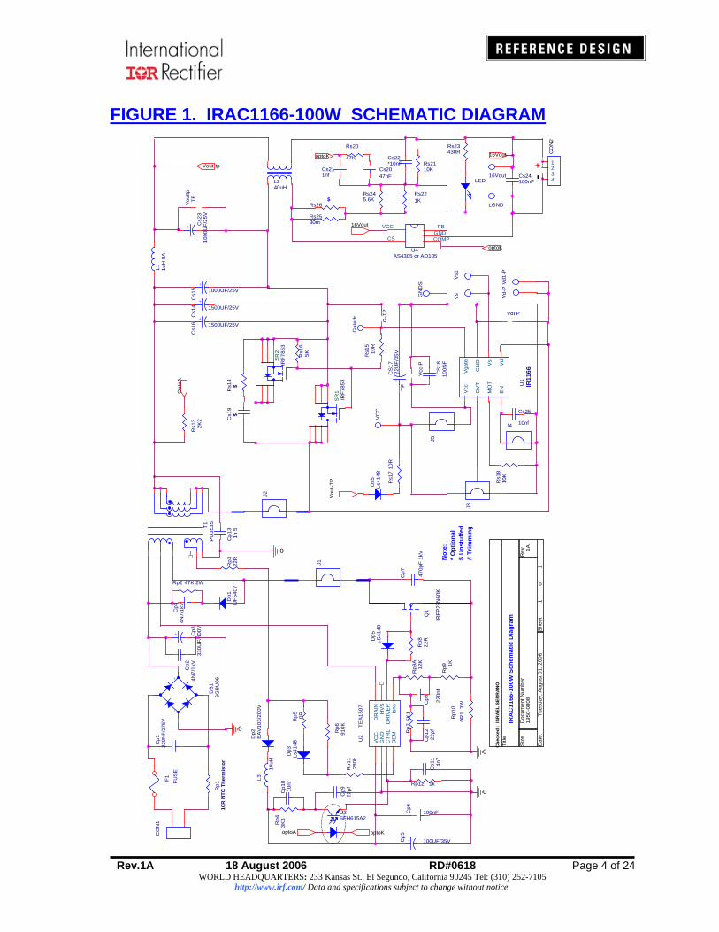
FIGURE 1. IRAC1166-100W SCHEMATIC DIAGRAM
#
Vout-tp
Rs20
47KRs2110K
Cs22*10nF
Cs211nf
Rs1
510
R
12
Dp5
LS41
48
Rs23430R
LED
Rp2 47K 2W
Cs2047nF
Cp4
4N7/
1kV
Rp3
22R
Vcc
-P
TPC
p7 470p
F 1k
V12
J51
2
CS
1810
0NF
12
10K
Rs1
8
12
J1
13
2J3
6 14
10 125 2
98711
3
T1P
Q35
35
Vd-
P
12
Rp6
910K
16Vout
G-T
P
Cp1
31n
5
Title
Siz
eD
ocum
ent N
umbe
rR
ev
Dat
e:S
heet
of
1950
-080
81A
IRA
C11
66-1
00W
Sch
emat
ic D
iagr
am
11
Tues
day,
Aug
ust 0
1, 2
006
+
CS
1722
UF/
35V
12
Rp5 0R
Vcc
1
OV
T2
MO
T3
EN
4V
d5
Vs
6G
ND
7V
gate
8
U1
IR11
66
Cs1
9$
0
Rs1
4$
12
Dp2
BA
V10
3/20
0V
Rs1
65K
0
12
J2
16Vout
12
Dp3
Ls41
48
0
Rs1
32K
2
Vd1
-P
+C
s16 1500UF/25V
+C
s14 1500UF/25V
+C
s15 1000UF/25V
Rp4
3K3
1 FB2 GND3 COMP4CS
5VCC
U4AS4305 or AQ105
Vs
Cp1
222
pf
Rs1
710
R
Cp1
010
nf
Vou
ttpTP
Cp9
22pf
VdTP
GN
DS
Vs1
Cp6
100nF
0
+Cp5
100UF/35V
21
L1 1uH
8A
1 2
Rp1
128
0k
+ Cs2
310
00U
F/25
V
21
L3
10uH
U3SFH615A2
4
123
5678
IRF7
853
SR
1
VC
C1
CTR
L3
DR
AIN
8
GN
D2
HV
S7
DR
IVE
R6
Isns
5D
EM
4
U2
TEA
1507
Rp12 1k
13
24 L2
40uH
Rp9
A12
K
Cp1
14n
7
Cp8 22
0nf
Che
cked
: IS
RA
EL S
ERR
AN
O
Gat
edr
Rp9 1K
Cs24100nF
4
123
5678
IRF7
853
SR
2
13
CO
N1
2
1
3
4-
+
DB
16G
BU
06
12 R
p75K
1
12
Rp1
10R
NTC
The
rmis
tor
1 2Cp1
220N
F/27
5V
21
Rp1
00R
1 3
W
F1 FUS
E
1 2
Ds5
Ls41
48
LGND
3
1
2
Q1
IRFP
22N
60K
12 Dp1
UF5
407
VC
C
11
22
33
44
CO
N2
Rs2530m
12
J4
Rs26$
Cp2
4N7/
1kV
1 2+ Cp3
330U
F/40
0V 12
Rp8
22R
optoA
Opt
oA
optoK
+
-
Cs25
10nf
Rs245.6K
Vou
t-TP
optoK
Rs221K
16Vout
optoK
Not
e:* O
ptio
nal
$ U
nstu
ffed
# Tr
imm
ing
Rev.1A 18 August 2006 RD#0618 Page 5 of 24 WORLD HEADQUARTERS: 233 Kansas St., El Segundo, California 90245 Tel: (310) 252-7105
http://www.irf.com/ Data and specifications subject to change without notice.
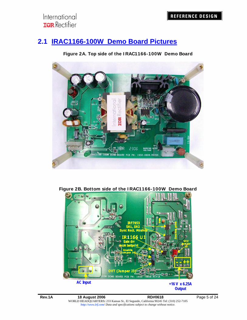
2.1 IRAC1166-100W Demo Board Pictures
Figure 2A. Top side of the IRAC1166-100W Demo Board
Figure 2B. Bottom side of the IRAC1166-100W Demo Board
AC Input +16 V x 6.25A
Output
- - ++
Rev.1A 18 August 2006 RD#0618 Page 6 of 24 WORLD HEADQUARTERS: 233 Kansas St., El Segundo, California 90245 Tel: (310) 252-7105
http://www.irf.com/ Data and specifications subject to change without notice.
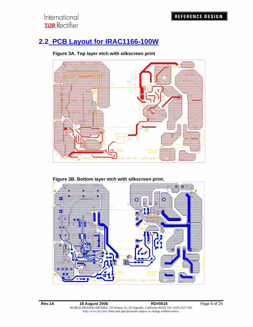
2.2 PCB Layout for IRAC1166-100W
Figure 3A. Top layer etch with silkscreen print
Figure 3B. Bottom layer etch with silkscreen print.

Rev.1A 18 August 2006 RD#0618 Page 7 of 24 WORLD HEADQUARTERS: 233 Kansas St., El Segundo, California 90245 Tel: (310) 252-7105
http://www.irf.com/ Data and specifications subject to change without notice.
3.0 CIRCUIT DESCRIPTION The PCB design is basically optimized as a test platform to evaluate of active rectification using Smart synchronous rectification and as well as basic features of flyback converter operating in quasi-resonant mode. This demo board has 2-pin connector ( CON1 ) for AC input and a time-lag type 3.5A fuse for input current overload protection. Minimum input filtering is provided (Cp1-Xcap) before AC input voltage (90-264VAC) is routed to a 6Amp-bridge rectifier (DB1). Primary side controller (U2) basically drives the primary Mosfet Q1 to operate in Critical-Conduction mode to eliminate turn-ON switching loss thru ZVS (zero voltage switching only occurs when NVsec > Vdcin ) or thru LVS ( low-voltage switching when nVsec< Vdcin) to reduce capacitive losses of Q1 especially at high line condition. The switching frequency Fsw at full load varies from ~38 to ~76kHz typically from low to high input condition and falls back to minimum value (fixed ~ 6 -10kHz) to reduce input power during light load condition. Auxiliary winding is loosely monitored by demagnetization pin4 of U2 through Dp3, Rp5 and Rp11 network that sets the OVP limit with Rp6 and Rp11 sets the over power limit of the converter. Resonant capacitor Cp7 is added to augment the overall parasitic winding capacitance and the primary mosfet Q1’s Coss to achieve ZVS and LVS at low and high input line condition respectively. Optocoupler U3 provides isolated output voltage feedback to the primary side. The output voltage level across load connector CON2 (+16Vo) is monitored and regulated by the V/I Secondary error amplifier U4 (AQ105 or AS4305) that also manages the output current limiting function by monitoring the voltage across the RS25-26 current sense resistors. The power stage of the secondary is using 2-SO8 low IRF7853 synch-fets (SR) in parallel to implement the low-side synchronous rectification. In this configuration, it is simpler to derive the Vcc supply for the U1 (IR1166 SO8-IC) controller directly from the DC output Vout. Jumper J5 is used to isolate U1’s Vcc from Vout so that user may easily evaluate IC’s power consumption especially during standby load condition. In the absence of a sensitive low current probe, the quiescent current Icc through Dp4 can be calculated from the differential voltage across the Rs17. The decoupling capacitor Cs17 and Cs18 provides additional filtering which is necessary to clean high frequency noise especially when U1 is driving several mosfets (SR1 // SR2) with high Qg parameters normally associated with high current-low voltage mosfets. The Vd and Vs sense pins monitor the voltage (Vsd) across the sync rect mosfets and proper attention was taken during PCB routing to ensure the integrity of differential voltage Vsd. This is done by directly taking the signal Vd from the drain pins of SR1//SR2 using a dedicated trace. Probe points as well as redundant test hook points are provided to facilitate easy probing of essential test waveforms.

Rev.1A 18 August 2006 RD#0618 Page 8 of 24 WORLD HEADQUARTERS: 233 Kansas St., El Segundo, California 90245 Tel: (310) 252-7105
http://www.irf.com/ Data and specifications subject to change without notice.
4.0 TEST CONNECTION AND SETUP DIAGRAM 4.1 Recommended setup for Voltage and Current probing
Fig. 4A Direct gate voltage
probing using tip & gnd spring.
Fig. 4C Connecting O-scope probe to
hook Gate drive test points.
Fig. 4B Recommended probing of
secondary current waveform.
Fig. 4D Recommended probing of Vout’s Ripple & Noise voltage.

Rev.1A 18 August 2006 RD#0618 Page 9 of 24 WORLD HEADQUARTERS: 233 Kansas St., El Segundo, California 90245 Tel: (310) 252-7105
http://www.irf.com/ Data and specifications subject to change without notice.
5.0 CIRCUIT FEATURES 5.1 OVT setting: The Offset Voltage Threshold can be easily selected by changing the position of jumper J3 according to system mode of operation as shown on Table 1 below. Since the demo board is practically designed to operate in Critical conduction mode, OVT pin can be left floating or grounded to prolong the MOSFET’s channel conduction period a bit compared 5to connecting it to Vcc. As a result, this would give the advantage of further reducing the conduction period of the MOSFET’s (SR1 & SR2) body diode, thus achieving more efficient operation. Reducing the chance of having reverse current during the fast turn-off phase of the sync-fets is another strong reason for having this feature available.
Table 1 System mode of operation OVT connected to
DCM or CrCM Ground, VTH1= -3.5mV Boundary CCM Floating, VTH1= -10.5mV
CCM VCC, VTH1= -19.0 mV The general observation during light load condition (~10-20% full load) is that a ~0.5 to ~1.2% efficiency improvement was seen for OVT=Gnd compared to OVT=floating. This small difference is no longer significant when the load becomes heavy for CrCM operation. 5.2 Enable setting: The IC is enabled by default knowing that EN pin is tied internally to VCC through a resistor. Having a jumper on J4 location will connect EN pin to Gnd and will immediately disable the internal gate drive circuit of the IR1166 IC. By putting a jumper J4 in/out would help the user to quickly evaluate the effect in efficiency by investigating the change in input power as a result of having SR fets working compared to just having an ordinary passive rectification offered by the body diode(s) when the gate drive is disabled. CAUTION : This demo board is basically designed for evaluation of functionality of IR1166 IC. The users may disable the IC by shorting J4 EN to GND for quick testing at full load but with care should be taken. It is strongly advise not to load more than 4.6 - 6Amp with IR1166 disabled for a prolong period of time (>1min). This is to prevent damaging the MOSFET’s body diode due to overheating when the load current passes through the mosfets’ body diode while SRs are turned-OFF. Never power-up the unit without shorting J5. 5.3 Minimum ON Time (MOT) setting: MOT setting is used to de-sensitize the IC from multiple change in Vsd during the turn-ON phase of SRs which is cause by the ringing of the secondary winding voltage (Vsec). MOT can be adjusted through Rs18 (according to AN1087 simplified equation RMOT = 2.5x10¹⁰ *tmot ) and is chosen to be 400 ns which is usually enough to ignore the parasitic noises at Vsd in a quasi-resonant switching converters such as this demo board.

Rev.1A 18 August 2006 RD#0618 Page 10 of 24 WORLD HEADQUARTERS: 233 Kansas St., El Segundo, California 90245 Tel: (310) 252-7105
http://www.irf.com/ Data and specifications subject to change without notice.
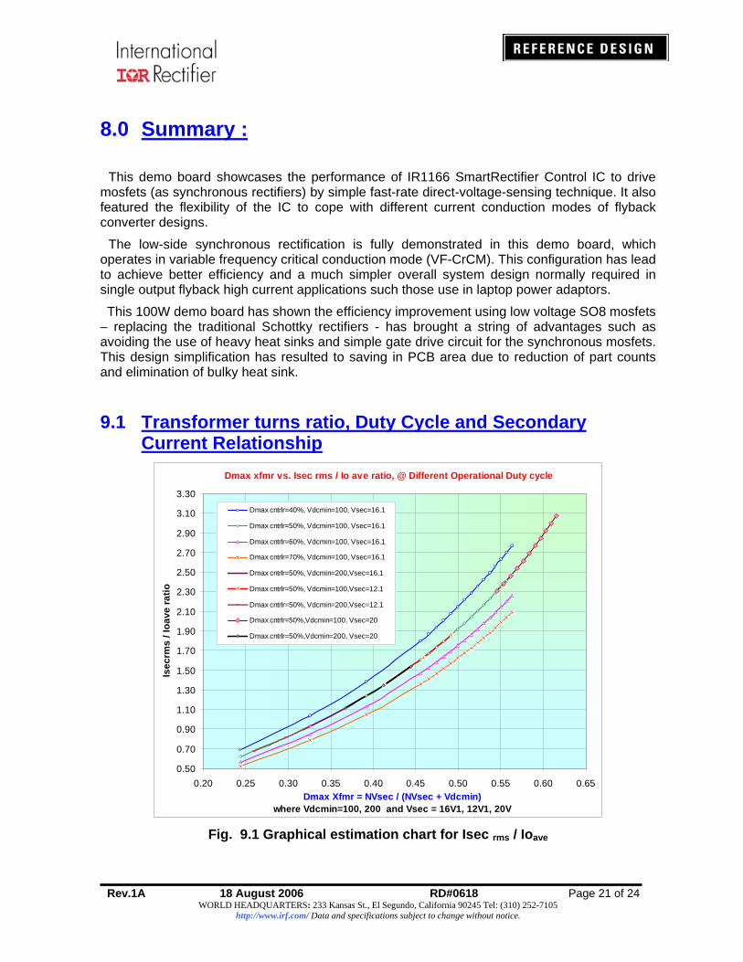
5.4 Mosfet Selection Design Tips Application note AN1087 has made it easy to understand the calculations required in flyback sync-rect driving circuits using IR1166 IC. Choosing the right mosfet(s) to satisfy the performance–cost requirement of any sync rect design should be simple as well. Voltage rating: SRs should also follow similar equation in most flyback design as shown below: Vsd > k*[Vo +(VDCinmax /(Npri/Nsec) )] where k =1.1 to 1.4 as a guard band for startup stress due to leakage spike. RdsON rating: Generally, it is easy to meet >1% system efficiency improvement if the conduction loss of the SRs becomes twice smaller than normal passive rectification approach. This is to achieve better thermal performance especially if the designer wishes to consider not having too bulky and heavy heatsink in the design, but take note that it would still be largely dependent on the size PCB copper area allotted to the SRs. We should also consider the estimated Rdson at 25˚C (normally shown in the datasheet) would be approximately ~1.8 times higher at Tj=125˚C. As a rule of thumb, we will base our calculation on these assumptions to simplify the mosfet selection criteria. For typical 100V Schottky rectifiers, Vf is around ~ 600 mV ( @Tj=125˚C), so in this case we should find a 100-V mosfet(s) with lower Rdson which will have a ~150mV max Vsd at rated full load current (Ioave). For quick estimation of Isecrms, designer might find Fig. 9.1 useful to quickly estimate Isecrms since Ioave is normally given as standard design specs.
Calculating the rms value of secondarycurrent is easier for CrCM mode where D = N*Vsec/ (N*Vsec + Vdcinmin) eqn. 1
N=Npri / Nsec , N = 31/5 Let Vsec =16.1, Vdcmin=100, D= ~50%h = Vf (Schottkydiode) / Vsd(mosfet ) eqn.2
Pdis SR < 1/h* Vfdiode* Ioave eqn.3
With h > 2, Target VSD(@Tj=125˚C) ≤ 600mV / 2 ≤ 300mV
I2secrms*RdsON (@Tj=125˚C) ≤ 300 mV*Ioave
eqn.4 RdsON (@Tj=125˚C) = ~1.8*RdsON (@Tj=25˚C) eqn.5
)1(3/)1(2
secD
DIoI ave
rms −−
= eqn.6
Combining equations 4, 5, and 6
aveCTjDSON Io
DmVR4
)]1(3[16625@
−≤
=
eqn.7
Ω==≤ 010.025.6
5.0*125.0%)50(*125.0
aveDSON Io
R
RdsON @Tj=25˚C ≤ 10 mΩ We can use 2-SO8 mosfets (IRF7853)in parallel having equivalent RdsON
(@Tj=25˚C) of ~9 mΩ. Note : Vsd(@Tj=125˚C)<100mV would yieldlower Rdson and can be achieve betterthermal performance but it would meanraising the parts count and cost.

Rev.1A 18 August 2006 RD#0618 Page 11 of 24 WORLD HEADQUARTERS: 233 Kansas St., El Segundo, California 90245 Tel: (310) 252-7105
http://www.irf.com/ Data and specifications subject to change without notice.
6.0 TEST WAVEFORMS 6.1.1 Transient Test
Fig 6A - 90 Vacin startup @ no load.
Ch1 : 50V/div, @ 90Vac Ch2 : 1V/div Vsd of sync rect (SR) Ch3 : 2V/div Vgate of SR1 & SR2 (IRF7853), F3: (zoom of Ch3) Ch4 ( x10A/V) =Isd ~54 Apk (max) 2.Vsd of sync rects are quite clean 3. The IR1166 IC start its sync rect oper’n only after ~3 msec from the first switching of the primary section. The body diodes of the sync rect mosfets act as the passive rectifiers during this particular period. The Gate drive (fsw : ~7.3kHz) pulses became so narrow after the output voltage stabilizes and reached the regulation at no load condition (-see Fig. 6G for more details). 4. Plot F4 is the zoom view of Ch4 (Isd) No significant reverse current during startup at full load.
Fig 6B - 265 Vacin –startup @ no load.
Ch1 : 50V/div, @265Vac Ch2 : 1V/div, Vsd of sync rect (SR) Ch3 : 2V/div, Vgate, F3: (zoom of Ch3) Ch4 ( x10A/V),Isd : ~38 Apk (max) 2. Vsd of sync-rects is uniform and switching regularly. 3. Gate drive pulses become narrow at light load condition and the switching frequency decreases after the output voltage reached its regulation level. 4. Plot F4 is the zoom view of Ch4 (Isd) - no significant reverse current during startup at full load. Narrow current pulses approx.~7 to 8Apk (see Fig 6H) is keeping the Vout within regulation during standby mode ( no load condition).
Rev.1A 18 August 2006 RD#0618 Page 12 of 24 WORLD HEADQUARTERS: 233 Kansas St., El Segundo, California 90245 Tel: (310) 252-7105
http://www.irf.com/ Data and specifications subject to change without notice.
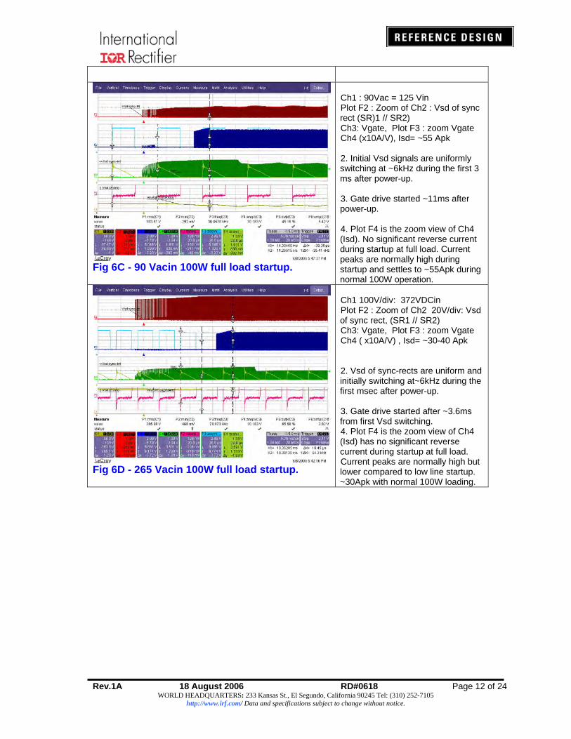
Fig 6C - 90 Vacin 100W full load startup.
Ch1 : 90Vac = 125 Vin Plot F2 : Zoom of Ch2 : Vsd of sync rect (SR)1 // SR2) Ch3: Vgate, Plot F3 : zoom Vgate Ch4 (x10A/V), Isd= ~55 Apk 2. Initial Vsd signals are uniformly switching at ~6kHz during the first 3 ms after power-up. 3. Gate drive started ~11ms after power-up. 4. Plot F4 is the zoom view of Ch4 (Isd). No significant reverse current during startup at full load. Current peaks are normally high during startup and settles to ~55Apk during normal 100W operation.
Fig 6D - 265 Vacin 100W full load startup.
Ch1 100V/div: 372VDCin Plot F2 : Zoom of Ch2 20V/div: Vsd of sync rect, (SR1 // SR2) Ch3: Vgate, Plot F3 : zoom Vgate Ch4 ( x10A/V) , Isd= ~30-40 Apk 2. Vsd of sync-rects are uniform and initially switching at~6kHz during the first msec after power-up. 3. Gate drive started after ~3.6ms from first Vsd switching. 4. Plot F4 is the zoom view of Ch4 (Isd) has no significant reverse current during startup at full load. Current peaks are normally high but lower compared to low line startup. ~30Apk with normal 100W loading.

Rev.1A 18 August 2006 RD#0618 Page 13 of 24 WORLD HEADQUARTERS: 233 Kansas St., El Segundo, California 90245 Tel: (310) 252-7105
http://www.irf.com/ Data and specifications subject to change without notice.
Fig 6E - Power down @ 90Vacin @ 100W full load
Ch1 : 90Vac = 125Vdc to ~44 Vdcin Ch2 : Vsd of sync rect (SR)1 // SR2) Ch3: Vgate,,, Plot F3 : zoom Vgate Ch4 @ x10A/V , Isd= ~56 Apk (max) 1. Switching stops after primary bulk voltage drops to ~40VDC. 2. (Plot F2) Vsd of sync-rects switching freq. at ~14kHz 3. Gate pulses stops probably due to IC’s UVLO threshold has been reached after Vout continuously dropped. 4. Plot F4 is the zoom view of Ch4. Isd rises as the output tries to maintain constant current while Vout start to drop until the IR1166 IC reach UVLO and sync rectification stops.
Fig 6F - Power down @ 265Vacin @ 100W full load
Ch1 : 100V/div Ch2 : 20V/div :VSD of sync rect (SR)1 // SR2) Ch3: Vgate, Plot F3 : zoom Vgate Ch4 (x10A/V), Isd= ~56 Apk (max) 1. Switching stops after primary bulk voltage drops to ~40VDC. 2. Vsd of sync-rects were switching at ~14kHz before IC‘s UVLO was reached. 3. Sync-rect gate drive also stops when the switching at the primary side ceases. 4. Ch4 is showing Isd rise from ~35Apk to ~56Apk before the unit completely shutdown.
Rev.1A 18 August 2006 RD#0618 Page 14 of 24 WORLD HEADQUARTERS: 233 Kansas St., El Segundo, California 90245 Tel: (310) 252-7105
http://www.irf.com/ Data and specifications subject to change without notice.
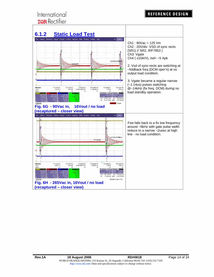
6.1.2 Static Load Test
Fig. 6G - 90Vac in, 16Vout / no load (recaptured – closer view)
Ch1 : 90Vac = 125 Vin Ch2 : 20V/div :VSD of sync rects (SR1) // SR2, IRF7853 ) Ch3: Vgate Ch4 ( x10A/V), Isd= ~5 Apk 2. Vsd of sync-rects are switching at ~foldback freq (DCM oper’n) at no output load condition. 3. Vgate became a regular narrow (~1.14us) pulses switching @~14kHz (fix freq. DCM) during no load standby operation.
Fig. 6H - 265Vac in, 16Vout / no load (recaptured – closer view)
Fsw falls back to a fix low frequency around ~6kHz with gate pulse width reduce to a narrow ~2usec at high line - no load condition.
Rev.1A 18 August 2006 RD#0618 Page 15 of 24 WORLD HEADQUARTERS: 233 Kansas St., El Segundo, California 90245 Tel: (310) 252-7105
http://www.irf.com/ Data and specifications subject to change without notice.
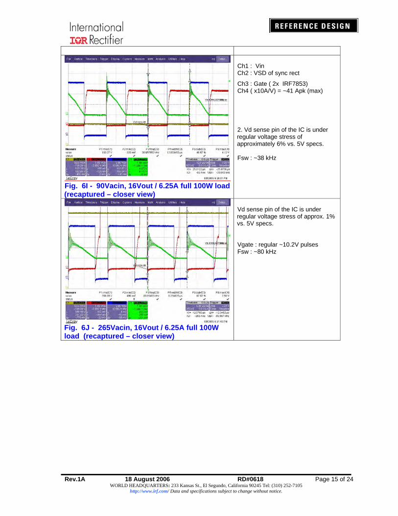
Fig. 6I - 90Vacin, 16Vout / 6.25A full 100W load (recaptured – closer view)
Ch1 : Vin Ch2 : VSD of sync rect
Ch3 : Gate ( 2x IRF7853) Ch4 ( x10A/V) = ~41 Apk (max)
2. Vd sense pin of the IC is under regular voltage stress of approximately 6% vs. 5V specs. Fsw : ~38 kHz
Fig. 6J - 265Vacin, 16Vout / 6.25A full 100W load (recaptured – closer view)
Vd sense pin of the IC is under regular voltage stress of approx. 1% vs. 5V specs. Vgate : regular ~10.2V pulses Fsw : ~80 kHz
Rev.1A 18 August 2006 RD#0618 Page 16 of 24 WORLD HEADQUARTERS: 233 Kansas St., El Segundo, California 90245 Tel: (310) 252-7105
http://www.irf.com/ Data and specifications subject to change without notice.
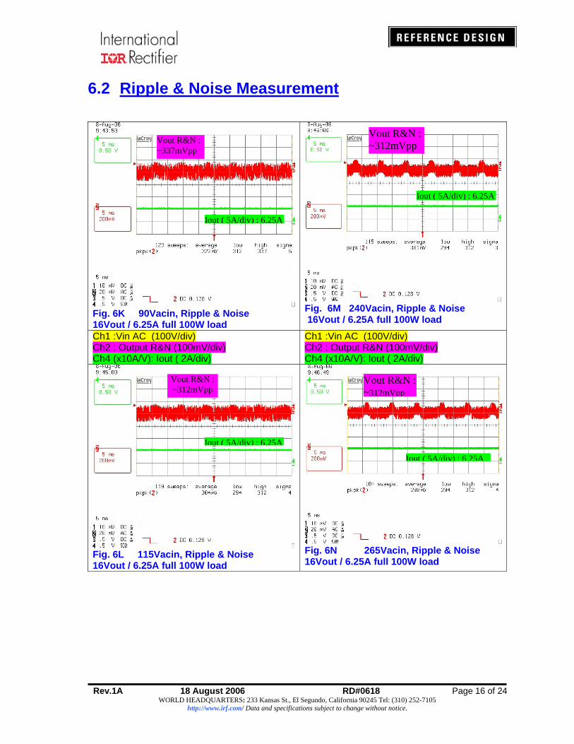
6.2 Ripple & Noise Measurement
Fig. 6K 90Vacin, Ripple & Noise 16Vout / 6.25A full 100W load
Fig. 6M 240Vacin, Ripple & Noise 16Vout / 6.25A full 100W load
Ch1 :Vin AC (100V/div) Ch2 : Output R&N (100mV/div) Ch4 (x10A/V): Iout ( 2A/div)
Ch1 :Vin AC (100V/div) Ch2 : Output R&N (100mV/div) Ch4 (x10A/V): Iout ( 2A/div)
Fig. 6L 115Vacin, Ripple & Noise 16Vout / 6.25A full 100W load
Fig. 6N 265Vacin, Ripple & Noise 16Vout / 6.25A full 100W load
Iout ( 5A/div) : 6.25A
Iout ( 5A/div) : 6.25A
Vout R&N : ~312mVpp Vout R&N :
~337mVpp
Iout ( 5A/div) : 6.25A
Iout ( 5A/div) : 6.25A
Vout R&N : ~312mVpp
Vout R&N : ~312mVpp

Rev.1A 18 August 2006 RD#0618 Page 17 of 24 WORLD HEADQUARTERS: 233 Kansas St., El Segundo, California 90245 Tel: (310) 252-7105
http://www.irf.com/ Data and specifications subject to change without notice.
6.3 Dynamic Load Test
( 0 – 100% rated load, +/- 800mA/usec)
Fig. 6O 90Vacin, Ripple & Noise +16Vout , 6.25A 5msec, 0A 5msec Fig. 5Q 240Vacin, Ripple & Noise
+16Vout , 6.25A 5msec, 0A 5msec Ch1 :Vin AC (100V/div) Ch2 : Output R&N (200mV/div) Ch4 (x10A/V): Iout ( 5A/div)
Ch1 :Vin AC (100V/div) Ch2 : Output R&N (200mV/div) Ch4 (x10A/V): Iout ( 5A/div)
Fig. 5P 115Vacin, Ripple & Noise +16Vout , 6.25A 5msec, 0A 5msec
Fig. 5R 265Vacin, Ripple & Noise +16Vout, 6.25A 5msec, 0A 5msec
Iout ( 5A/div)
Vout R&N : 869mVpp
Vout R&N : 831mVpp
Vout R&N : 812mVpp
Vout R&N : 806mVpp
Iout ( 5A/div)
Iout ( 5A/div) Iout ( 5A/div)
Rev.1A 18 August 2006 RD#0618 Page 18 of 24 WORLD HEADQUARTERS: 233 Kansas St., El Segundo, California 90245 Tel: (310) 252-7105
http://www.irf.com/ Data and specifications subject to change without notice.
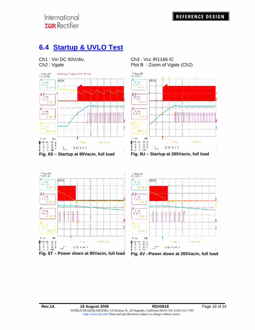
6.4 Startup & UVLO Test Ch1 : Vin DC 50V/div, Ch2 : Vgate
Fig. 6S – Startup at 90Vacin, full load
Fig. 6T – Power down at 90Vacin, full load
Ch3 : Vcc IR1166 IC Plot B : Zoom of Vgate (Ch2)
Fig. 6U – Startup at 265Vacin, full load Possible
Fig. 6V –Power down at 265Vacin, full load Spurious

Rev.1A 18 August 2006 RD#0618 Page 19 of 24 WORLD HEADQUARTERS: 233 Kansas St., El Segundo, California 90245 Tel: (310) 252-7105
http://www.irf.com/ Data and specifications subject to change without notice.
7.0 LINE/ LOAD REGULATION TEST
Figure 7.1. Output Voltage vs. Load Current Characteristic Curve
7.1 IR1166 Demo Board V-I Characteristics Table 2
Vin 90 115 180 220 230 265 Iout (A) Vout (V) Vout (V) Vout (V) Vout (V) Vout (V) Vout (V)
0 16.12 16.11 16.12 16.12 16.12 16.12
1 16.12 16.12 16.12 16.12 16.12 16.12
2 16.12 16.12 16.12 16.12 16.12 16.12
3 16.12 16.12 16.12 16.12 16.12 16.12
4 16.12 16.12 16.12 16.12 16.12 16.12
5 16.11 16.11 16.12 16.12 16.11 16.12
6 16.09 16.09 16.09 16.10 16.10 16.10
6.25 16.09 16.09 16.10 16.10 16.10 16.10
6.5 16.09 16.10 16.11 16.11 16.11 16.11
6.75 13.91 13.82 13.91 13.88 13.93 13.98
7 10.60 10.58 10.55 10.66 10.73 10.78
7.25 Bounce Bounce Bounce Bounce Bounce Bounce
IRAC1166-100W Demo Board V / ICharacteristic Curve
0123456789
1011121314151617
0 1 2 3 4 5 6 7 8Output Load Current (A)
Out
put V
olta
ge (V
) 90Vac115Vac180VAc220Vac230Vac265Vac
Rev.1A 18 August 2006 RD#0618 Page 20 of 24 WORLD HEADQUARTERS: 233 Kansas St., El Segundo, California 90245 Tel: (310) 252-7105
http://www.irf.com/ Data and specifications subject to change without notice.
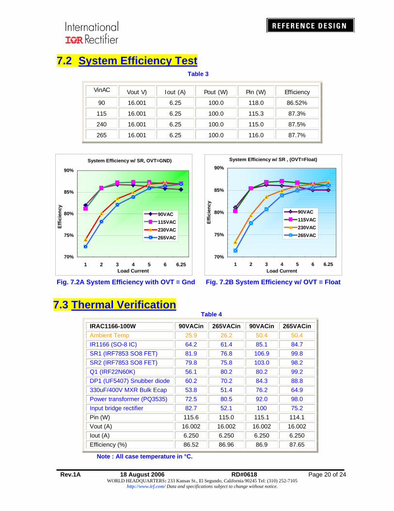
7.2 System Efficiency Test Table 3
VinAC Vout V) Iout (A) Pout (W) Pin (W) Efficiency
90 16.001 6.25 100.0 118.0 86.52%
115 16.001 6.25 100.0 115.3 87.3%
240 16.001 6.25 100.0 115.0 87.5%
265 16.001 6.25 100.0 116.0 87.7%
System Efficiency w/ SR, OVT=GND)
70%
75%
80%
85%
90%
1 2 3 4 5 6 6.25Load Current
Effic
ienc
y
90VAC115VAC230VAC265VAC
7.3 Thermal Verification Table 4
IRAC1166-100W 90VACin 265VACin 90VACin 265VACin Ambient Temp 25.9 26.2 50.4 50.4 IR1166 (SO-8 IC) 64.2 61.4 85.1 84.7 SR1 (IRF7853 SO8 FET) 81.9 76.8 106.9 99.8 SR2 (IRF7853 SO8 FET) 79.8 75.8 103.0 98.2 Q1 (IRF22N60K) 56.1 80.2 80.2 99.2 DP1 (UF5407) Snubber diode 60.2 70.2 84.3 88.8 330uF/400V MXR Bulk Ecap 53.8 51.4 76.2 64.9 Power transformer (PQ3535) 72.5 80.5 92.0 98.0 Input bridge rectifier 82.7 52.1 100 75.2 Pin (W) 115.6 115.0 115.1 114.1 Vout (A) 16.002 16.002 16.002 16.002 Iout (A) 6.250 6.250 6.250 6.250 Efficiency (%) 86.52 86.96 86.9 87.65
Note : All case temperature in °C.
Fig. 7.2B System Efficiency w/ OVT = FloatFig. 7.2A System Efficiency with OVT = Gnd
System Efficiency w/ SR , (OVT=Float)
70%
75%
80%
85%
90%
1 2 3 4 5 6 6.25Load Current
Effic
ienc
y90VAC115VAC230VAC265VAC
Rev.1A 18 August 2006 RD#0618 Page 21 of 24 WORLD HEADQUARTERS: 233 Kansas St., El Segundo, California 90245 Tel: (310) 252-7105
http://www.irf.com/ Data and specifications subject to change without notice.
8.0 Summary :
This demo board showcases the performance of IR1166 SmartRectifier Control IC to drive mosfets (as synchronous rectifiers) by simple fast-rate direct-voltage-sensing technique. It also featured the flexibility of the IC to cope with different current conduction modes of flyback converter designs.
The low-side synchronous rectification is fully demonstrated in this demo board, which operates in variable frequency critical conduction mode (VF-CrCM). This configuration has lead to achieve better efficiency and a much simpler overall system design normally required in single output flyback high current applications such those use in laptop power adaptors.
This 100W demo board has shown the efficiency improvement using low voltage SO8 mosfets – replacing the traditional Schottky rectifiers - has brought a string of advantages such as avoiding the use of heavy heat sinks and simple gate drive circuit for the synchronous mosfets. This design simplification has resulted to saving in PCB area due to reduction of part counts and elimination of bulky heat sink. 9.1 Transformer turns ratio, Duty Cycle and Secondary
Current Relationship Dmax xfmr vs. Isec rms / Io ave ratio, @ Different Operational Duty cycle
0.50
0.70
0.90
1.10
1.30
1.50
1.70
1.90
2.10
2.30
2.50
2.70
2.90
3.10
3.30
0.20 0.25 0.30 0.35 0.40 0.45 0.50 0.55 0.60 0.65Dmax Xfmr = NVsec / (NVsec + Vdcmin)
where Vdcmin=100, 200 and Vsec = 16V1, 12V1, 20V
Isec
rms
/ Ioa
ve ra
tio
Dmax cntrlr=40%, Vdcmin=100, Vsec=16.1
Dmax cntrlr=50%, Vdcmin=100, Vsec=16.1
Dmax cntrlr=60%, Vdcmin=100, Vsec=16.1
Dmax cntrlr=70%, Vdcmin=100, Vsec=16.1
Dmax cntrlr=50%, Vdcmin=200,Vsec=16.1
Dmax cntrlr=50%, Vdcmin=100,Vsec=12.1
Dmax cntrlr=50%, Vdcmin=200,Vsec=12.1
Dmax cntrlr=50%,Vdcmin=100, Vsec=20
Dmax cntrlr=50%,Vdcmin=200, Vsec=20
Fig. 9.1 Graphical estimation chart for Isec rms / Ioave
Rev.1A 18 August 2006 RD#0618 Page 22 of 24 WORLD HEADQUARTERS: 233 Kansas St., El Segundo, California 90245 Tel: (310) 252-7105
http://www.irf.com/ Data and specifications subject to change without notice.
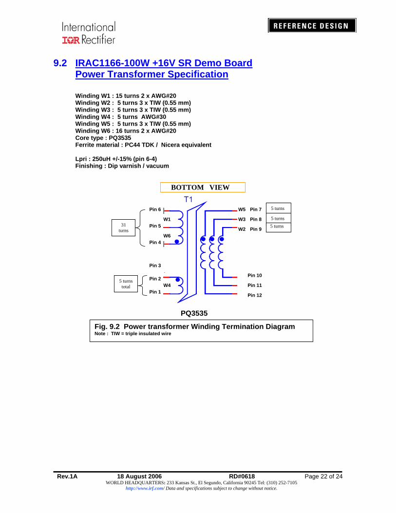
9.2 IRAC1166-100W +16V SR Demo Board
Power Transformer Specification Winding W1 : 15 turns 2 x AWG#20 Winding W2 : 5 turns 3 x TIW (0.55 mm) Winding W3 : 5 turns 3 x TIW (0.55 mm) Winding W4 : 5 turns AWG#30 Winding W5 : 5 turns 3 x TIW (0.55 mm) Winding W6 : 16 turns 2 x AWG#20 Core type : PQ3535 Ferrite material : PC44 TDK / Nicera equivalent Lpri : 250uH +/-15% (pin 6-4) Finishing : Dip varnish / vacuum
PQ3535
W1
W6
W3
W5
W4
W2
Pin 6
Pin 5
Pin 4
Pin 3
Pin 2
Pin 1
Pin 7
Pin 8
Pin 9
Pin 10
Pin 11
Pin 12
BOTTOM VIEW
31 turns
5 turns total
5 turns
5 turns 5 turns
Fig. 9.2 Power transformer Winding Termination Diagram Note : TIW = triple insulated wire
Rev.1A 18 August 2006 RD#0618 Page 23 of 24 WORLD HEADQUARTERS: 233 Kansas St., El Segundo, California 90245 Tel: (310) 252-7105
http://www.irf.com/ Data and specifications subject to change without notice.
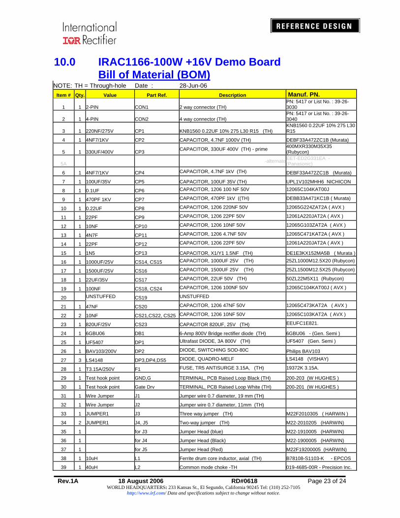
10.0 IRAC1166-100W +16V Demo Board Bill of Material (BOM)
NOTE: TH = Through-hole Date : 28-Jun-06 Item # Qty. Value Part Ref. Description Manuf. PN.
1 1 2-PIN CON1 2 way connector (TH) PN: 5417 or List No. : 39-26-3030
2 1 4-PIN CON2 4 way connector (TH) PN: 5417 or List No. : 39-26-3040
3 1 220NF/275V CP1 KNB1560 0.22UF 10% 275 L30 R15 (TH) KNB1560 0.22UF 10% 275 L30 R15
4 1 4NF7/1KV CP2 CAPACITOR, 4.7NF 1000V (TH) DEBF33A472ZC1B (Murata)
5 1 330UF/400V CP3 CAPACITOR, 330UF 400V (TH) - prime 400MXR330M35X35 (Rubycon)
5A -alternateEET-ED2G331EA - (Panasonic)
6 1 4NF7/1KV CP4 CAPACITOR, 4.7NF 1kV (TH) DEBF33A472ZC1B (Murata)
7 1 100UF/35V CP5 CAPACITOR, 100UF 35V (TH) UPL1V102MHH6 NICHICON
8 1 0.1UF CP6 CAPACITOR, 1206 100 NF 50V 12065C104KAT00J
9 1 470PF 1KV CP7 CAPACITOR, 470PF 1kV ((TH) DEBB33A471KC1B ( Murata)
10 1 0.22UF CP8 CAPACITOR, 1206 220NF 50V 12065G224ZAT2A ( AVX )
11 1 22PF CP9 CAPACITOR, 1206 22PF 50V 12061A220JAT2A ( AVX )
12 1 10NF CP10 CAPACITOR, 1206 10NF 50V 12065G103ZAT2A ( AVX )
13 1 4N7F CP11 CAPACITOR, 1206 4.7NF 50V 12065C471KAT2A ( AVX )
14 1 22PF CP12 CAPACITOR, 1206 22PF 50V 12061A220JAT2A ( AVX )
15 1 1N5 CP13 CAPACITOR, X1/Y1 1.5NF (TH) DE1E3KX152MA5B ( Murata )
16 1 1000UF/25V CS14, CS15 CAPACITOR, 1000UF 25V (TH) 25ZL1000M12.5X20 (Rubycon)
17 1 1500UF/25V CS16 CAPACITOR, 1500UF 25V (TH) 25ZL1500M12.5X25 (Rubycon)
18 1 22UF/35V CS17 CAPACITOR, 22UF 50V (TH) 50ZL22M5X11 (Rubycon)
19 1 100NF CS18, CS24 CAPACITOR, 1206 100NF 50V 12065C104KAT00J ( AVX )
20 UNSTUFFED CS19 UNSTUFFED 2222 680 34689. BCE-SUD
21 1 47NF CS20 CAPACITOR, 1206 47NF 50V 12065C473KAT2A ( AVX )
22 2 10NF CS21,CS22, CS25 CAPACITOR, 1206 10NF 50V 12065C103KAT2A ( AVX )
23 1 820UF/25V CS23 CAPACITOR 820UF, 25V (TH) EEUFC1E821.
24 1 6GBU06 DB1 6-Amp 800V Bridge rectifier diode (TH) 6GBU06 - (Gen. Semi )
25 1 UF5407 DP1 Ultrafast DIODE, 3A 800V (TH) UF5407 (Gen. Semi )
26 1 BAV103/200V DP2 DIODE, SWITCHING SOD-80C Philips BAV103
27 3 LS4148 DP3,DP4,DS5 DIODE, QUADRO-MELF LS4148 (VISHAY)
28 1 T3.15A/250V F1 FUSE, TR5 ANTISURGE 3.15A, (TH) 19372K 3.15A.
29 1 Test hook point GND,G TERMINAL, PCB Raised Loop Black (TH) 200-203 (W HUGHES )
30 1 Test hook point Gate Drv TERMINAL, PCB Raised Loop White (TH) 200-201 (W HUGHES )
31 1 Wire Jumper J1 Jumper wire 0.7 diameter, 19 mm (TH)
32 1 Wire Jumper J2 Jumper wire 0.7 diameter, 11mm (TH)
33 1 JUMPER1 J3 Three way jumper (TH) M22F2010305 ( HARWIN )
34 2 JUMPER1 J4, J5 Two-way jumper (TH) M22-2010205 (HARWIN)
35 1 for J3 Jumper Head (blue) M22-1910005 (HARWIN)
36 1 for J4 Jumper Head (Black) M22-1900005 (HARWIN)
37 1 for J5 Jumper Head (Red) M22F19200005 (HARWIN)
38 1 10uH L1 Ferrite drum core inductor, axial (TH) B78108-S1103-K - EPCOS
39 1 40uH L2 Common mode choke -TH 019-4685-00R - Precision Inc.
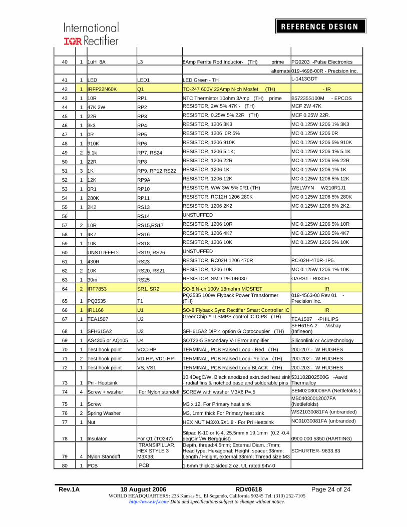
Rev.1A 18 August 2006 RD#0618 Page 24 of 24 WORLD HEADQUARTERS: 233 Kansas St., El Segundo, California 90245 Tel: (310) 252-7105
http://www.irf.com/ Data and specifications subject to change without notice.
40 1 1uH 8A L3 8Amp Ferrite Rod Inductor- (TH) prime PG0203 -Pulse Electronics
alternate019-4698-00R - Precision Inc.
41 1 LED LED1 LED Green - TH L-1413GDT
42 1 IRFP22N60K Q1 TO-247 600V 22Amp N-ch Mosfet (TH) - IR
43 1 10R RP1 NTC Thermistor 10ohm 3Amp (TH) prime B57235S100M - EPCOS
44 1 47K 2W RP2 RESISTOR, 2W 5% 47K - (TH) MCF 2W 47K
45 1 22R RP3 RESISTOR, 0.25W 5% 22R (TH) MCF 0.25W 22R.
46 1 3k3 RP4 RESISTOR, 1206 3K3 MC 0.125W 1206 1% 3K3
47 1 0R RP5 RESISTOR, 1206 0R 5% MC 0.125W 1206 0R
48 1 910K RP6 RESISTOR, 1206 910K MC 0.125W 1206 5% 910K
49 2 5.1k RP7, RS24 RESISTOR, 1206 5.1K; MC 0.125W 1206 1% 5.1K
50 1 22R RP8 RESISTOR, 1206 22R MC 0.125W 1206 5% 22R
51 3 1K RP9, RP12,RS22 RESISTOR, 1206 1K MC 0.125W 1206 1% 1K
52 1 12K RP9A RESISTOR, 1206 12K MC 0.125W 1206 5% 12K
53 1 0R1 RP10 RESISTOR, WW 3W 5% 0R1 (TH) WELWYN W210R1J1
54 1 280K RP11 RESISTOR, RC12H 1206 280K MC 0.125W 1206 5% 280K
55 1 2K2 RS13 RESISTOR, 1206 2K2 MC 0.125W 1206 5% 2K2.
56 RS14 UNSTUFFED
57 2 10R RS15,RS17 RESISTOR, 1206 10R MC 0.125W 1206 5% 10R
58 1 4K7 RS16 RESISTOR, 1206 4K7 MC 0.125W 1206 5% 4K7
59 1 10K RS18 RESISTOR, 1206 10K MC 0.125W 1206 5% 10K
60 UNSTUFFED RS19, RS26 UNSTUFFED
61 1 430R RS23 RESISTOR, RC02H 1206 470R RC-02H-470R-1P5.
62 2 10K RS20, RS21 RESISTOR, 1206 10K MC 0.125W 1206 1% 10K
63 1 30m RS25 RESISTOR, SMD 1% 0R030 OARS1 - R030FI.
64 2 IRF7853 SR1, SR2 SO-8 N-ch 100V 18mohm MOSFET IR
65 1 PQ3535 T1 PQ3535 100W Flyback Power Transformer (TH)
019-4563-00 Rev 01 -Precision Inc.
66 1 IR1166 U1 SO-8 Flyback Sync Rectifier Smart Controller IC IR
67 1 TEA1507 U2 GreenChip™ II SMPS control IC DIP8 (TH) TEA1507 -PHILIPS
68 1 SFH615A2 U3 SFH615A2 DIP 4 option G Optocoupler (TH) SFH615A-2 -Vishay (Infineon)
69 1 AS4305 or AQ105 U4 SOT23-5 Secondary V-I Error amplifier Siliconlink or Acutechnology
70 1 Test hook point VCC-HP TERMINAL, PCB Raised Loop - Red (TH) 200-207 - W HUGHES
71 2 Test hook point VD-HP, VD1-HP TERMINAL, PCB Raised Loop- Yellow (TH) 200-202 - W HUGHES
72 1 Test hook point VS, VS1 TERMINAL, PCB Raised Loop BLACK (TH) 200-203 - W HUGHES
73 1 Pri - Heatsink 10.4DegC/W, Black anodized extruded heat sink - radial fins & notched base and solderable pins
531102B02500G -Aavid Thermalloy
74 4 Screw + washer For Nylon standoff SCREW with washer M3X6 P=.5 SEM02030006FA (Nettlefolds )
75 1 Screw M3 x 12, For Primary heat sink MB04030012007FA (Nettlefolds)
76 2 Spring Washer M3, 1mm thick For Primary heat sink WS21030081FA (unbranded)
77 1 Nut HEX NUT M3X0.5X1.8 - For Pri Heatsink NC01030081FA (unbranded)
78 1 Insulator For Q1 (TO247) Silpad K-10 or K-4, 25.5mm x 19.1mm (0.2 -0.4 degCin2/W Bergquist) 0900 000 5350 (HARTING)
79 4 Nylon Standoff
TRANSIPILLAR, HEX STYLE 3 M3X38;
Depth, thread:4.5mm; External Diam.,:7mm; Head type: Hexagonal; Height, spacer:38mm; Length / Height, external:38mm; Thread size:M3
SCHURTER- 9633.83
80 1 PCB PCB 1.6mm thick 2-sided 2 oz, UL rated 94V-0