Embed Size (px)
Citation preview
Reduction of Mutual Coupling between Radiating
Elements of an Array Antenna Using EBG
Electromagnetic Band Structures
Sara Said, Abdenacer Es-salhi, and Mohammed Elhitmy
Department of Physics, University of Mohamed Premier, Oujda, Morocco
Email: [email protected]; [email protected]
Abstract—In this paper, a new array antenna configuration based on Electromagnetic Band Gap (EBG) structures has been proposed for 3.5GHz wireless communication systems. The proposed slotted EBG structure, high impedance surface (SHI), consists of three squares and a square ring deposited on a substrate (Rogers RO4350) which has a relative permittivity of 10.2 and a thickness of 1.27mm. Initially a matrix of 3×7 unit cells of EBG structures is introduced between two patches of an array and then a matrix of 3×14 unit cell of EBG structures is integrated between eight patches, which resonate around 3.5GHz (Wi MAX). The insertion of these structures between the radiating elements of an array antenna reduces the mutual coupling and antenna dimensions by approximately (8dB, 11%) and (12 dB, 5%) respectively for two, eight elements array antenna. In addition, the directivity has been slightly improved in the presence of EBG structures, from 4.52dB to 6.09dB for a two-element array antenna, and from 8.18dB to
8.4dB for an eight-element antenna.
Index Terms—Antenna array, electromagnetic band gap structure, mutual coupling, radiation pattern
I. INTRODUCTION
Several scientific studies have been conducted to improve the radiation performance of antenna arrays. The antenna printed on an isotropic substrate has been the subject of a certain number of research works during the last decades, the concept of the radiating structure was first studied by Deschamps in 1950 [1], [2]. The development of methods to reduce the mutual coupling between radiating sources has become a topical issue. Microstrip antenna array is widely used in several communication systems such as mobile telephony, wireless multimedia systems (WiFi, Bluetooth) and also space communications, and radar applications. However, as the separations between the array elements are reduced, the mutual coupling between the antennas caused by surface waves becomes stronger. Therefore, the use of high impedance surface (SHI) type electromagnetic band gap structures may be a solution. The SHI (high impedance surface) structure was proposed by Sievenpiper in [3], it consists of four parts: a ground plane, a dielectric substrate, metal plates and connection
Manuscript received May 16, 2020; revised August 8, 2020;
accepted August 18, 2020.
Corresponding author: Sara Said (email: [email protected]).
vias. To analyze the characteristics of the SHI (high impedance surface) structure, different methods have been implemented. These methods can be classified into three categories: a model based on the equivalent circuit [4], [5], a model based on the transmission line [6]-[8] and a model based on the periodic boundary conditions [9]. The model of the equivalent circuit is the simplest one, which describes the SHI structure as an LC resonant circuit. The values of inductance L and capacitance C are determined by the SHI (high impedance surface) geometry, and its resonance behavior is used to explain the band gap characteristic of the SHI structure. This model is simple to understand, but the results are not very accurate due to the simplified approximation of L and C.
This structure has interesting behaviors in microwave frequencies [3], [10], it is applied to reject frequency bands [11] and avoid unwanted electromagnetic waves from propagating [12]. The suppression of surface waves helps to improve the performance of an antenna by increasing the antenna gain and reducing the return radiation [13]. Various SHI (high impedance surface) structures have been extensively studied in the last decade [14]-[16]. Other types of structures can play the same role. For example in references [17] and [18], there is about 16 dB of mutual coupling attenuation obtained by inserting slots in the ground plane Defected Ground Structure (DGS), but the back-lobe radiation is increased due to the existence of the slots in the ground plane, whereas Electromagnetic Band Gap (EBG) structures are a good choice for mutual coupling reduction between the radiating elements [19]-[22], which in turn improves antenna performance.
This paper focuses on the one hand on reducing the mutual coupling between two antenna arrays each containing four microstrip patch antennas and on the other hand on improving array antenna performance by using EBG electromagnetic band gap structures as shown in Fig. 1.
Fig. 1. The integration of the EBG and the antenna array
International Journal of Electrical and Electronic Engineering & Telecommunications Vol. 10, No. 2, March 2021
©2021 Int. J. Elec. & Elecn. Eng. & Telcomm. 91doi: 10.18178/ijeetc.10.2.91-98

The proposed structure is printed on a Rogers RO4350
substrate with a dielectric constant of 10.2 and thickness
h=1.27mm. We present in this paper the results of the
simulations which will be discussed in Section II, III and
Section IV.
II. CONFIGURATION AND DESIGN OF THE EBG
STRUCTURE
The slot-loaded EBG structure is a new type of electromagnetic band gap structures which are designed by adding some slots in the metal plates of conventional mushroom like EBG. These slots affect the one hand the current distribution on the patches resulting in a longer current path, and on the other hand they create additional capacitance formed between the edges of the slots. In this paper, we designed a new EBG slotted structure by introducing three squares and a square ring deposited on a substrate (Rogers RO4350) which has a relative permittivity 10.2 and a thickness of 1.27mm. The width of the three squares is 0.8mm, while 0.3mm is the width of the ring. The unit cell of the EBG structure is illustrated in Fig. 2 and the summary of the parametric values of this cell is presented in the Table I.
The equivalent circuit model describes the EBG structure as an LC resonant circuit. An electromagnetic wave which strikes the structure causes electric fields to cover the narrow spaces between the neighboring metal plates and this causes the accumulation of charges on the ends of the metal patches, which can be described as an effective capacitance C. The charges which go back, circulate around the conducting paths through the vias and the ground plane, describing an inductance L associated with the conduction currents. The whole forms a parallel resonant circuit which dictates the electromag-netic behavior of the EBG structure as shown in Fig. 3.
Fig. 2. Configuration of the EBG unit cell (top and side views)
TABLE I: DESCRIBES THE SUMMARY OF THE PARAMETRIC VALUES OF
THE EBG UNIT CELL
Parameters description Values (mm)
ic thickness of interior squares 0.8
i thickness of the square ring 0.3
g The space between the unit cells 0.2
Wp Length or width (Wp) of the unit cell 6.4
h Substrate thickness 1.27
m Ground plane thickness 0.0175
r Via radius 0.5
Fig. 3. Equivalent electric model.
The initial inductance L and capacitance C of the
conventional mushroom-like EBG structure are [23]:
0 rL h (1)
10 (1 )cosh
π
rw w gC
g
(2)
where ε0 and μ0 are the permittivity and permeability of
the free space respectively, the parameter g represents the
gap between the elements of the EBG structure and w
represents the width of the patch.
The inductance and capacitance equivalents are equal
to the inductance and capacitance of the conventional
mushroom-like structure, in addition to the new L and C
which are created by the slots. Thus by inserting the slots
the initial value of L and C remains unchanged while the
value of equivalent L and C will increase and cause a
lower resonant frequency and finally a compact structure.
The resonance frequency of the equivalent circuit is
given by
1
LC (3)
And the bandwidth of the band gap frequency is expressed as
1W
LB
C
(4)
where η is the impedance of the free space.
The surface impedance being defined by effective
equivalent circuit parameters which are determined by the
geometry of the surface texture. Capacitors are formed by
fringed electric fields between adjacent metal patches.
The inductance is fixed by the thickness of the structure.
According to Sievenpiper [12], the surface impedance is
given by the following expression:
21
j LZ
LC
(5)
To get the accurate band gap characteristics, the design
parameters of the unit cell illustrated in Fig. 2 have been
optimized so that the band gap frequency interval
contains the Wi MAX band. See Fig. 4.
Fig. 4. Transmission coefficient S21 of the EBG unit cell.
International Journal of Electrical and Electronic Engineering & Telecommunications Vol. 10, No. 2, March 2021
©2021 Int. J. Elec. & Elecn. Eng. & Telcomm. 92

Fig. 5. Designing steps of the EBG unit cell.
From Fig. 4 we can see that the transmission
coefficient S21 is less that 20dB, between 3.2GHz and
3.4GHz, indicates the behavior of the EBG structure that
acts like a stop band filter in order to obtain a rejection
around these frequencies.
The proposed EBG was obtained in four successive
steps as demonstrated by Fig. 5. It is clear that the
proposed EBG is designed by creating three squares and a
square ring in the metal plates of conventional mushroom
like EBG. These slots are created to achieve better
antenna performance parameters. (See Fig. 9 in the
section III-B).
III. TWO-ELEMENT ARRAY ANTENNA WITH AND
WITHOUT EBG STRUCTURE
A. Two-Element Array Antenna Design
Printed antennas are widely used in wireless
communications because of their advantages: low profile,
light weight, planar structure and low cost, they also have
some disadvantages, such as narrow bandwidth and low
gain. To meet the requirements of long distance
communication, it is necessary to design antennas with
very high gain. The array antenna model is considered to
be one of the simplest ways to improve gain and
bandwidth, but these improvements introduce mutual
coupling between patches, which can reduce array
efficiency. To see the effect of the EBG structure SHI-
type on the coupling between antennas, we must first
study the coupling between two printed antennas
resonating at 3.5GHz. The array antenna geometry and
parameters are illustrated in Fig. 6
Fig. 6. Two patches resonating at 3.5GHz on a substrate of εr =10.2, W=
70mm, L = 25.3mm, lp =12.65mm, wp = 18.11 mm, wf = 1mm, Lf =
8mm, d = 26.86mm (d=1 λ3.5).
3,2 3,3 3,4 3,5 3,6 3,7 3,8
-40
-35
-30
-25
-20
-15
-10
S-parameter [Magnitude in dB]
/
Frequency / GHz
S12--d=16,11mm: - 15,76 dB
S12--d=19,33 mm: -18,69 dB
S12--d=21,48 mm: -19,87 dB
S12--d=26,86 mm: -24,41 dB
Fig. 7. Variation of mutual coupling depending on the distance d
between two array antennas.
Fig. 8. Over view of the EBG structure, W=62.37mm, L=L= 25.3mm,
d= 19.33mm (d= 0.72λ3.5).
B. Reduction of Mutual Coupling Using Slotted EBG
To study the variation of the mutual coupling as a
function of the distance d between the two radiating
elements, first we take a distance d = 26.86mm (1.0 λ3.5
GHz) between the two antennas, a weak mutual coupling
exists between radiant elements.
Then for d=21.48mm (0.8 λ3.5 GHz), d = 19.33mm
(0.72 λ3.5 GHz) and d = 16.11mm (0.6 λ3.5 GHz), it can be
seen from Fig.7 that as the distance between the two array
elements decreases, the mutual coupling increases. In
conclusion, the mutual coupling between two radiating
elements depends on the distance between them.
The surface waves generated have a significant effect
on the mutual coupling between the elements of the
antenna array. Especially in the case of array elements on
high permittivity substrates. The introduction of the EBG
structure between the array elements has shown its ability
to suppress surface waves and to reduce mutual coupling
at the resonant frequency, knowing that the distance
between the two elements is reduced to d=19.33mm (this
distance is chosen because it gives a better reduction of
mutual coupling between the radiating elements). A
matrix of 3×7 unit cells of EBG structures are inserted
between two patch antennas to reduce mutual coupling,
as shown in Fig. 8. From Fig. 8 we can see that the
antenna dimension is reduced around 11%.
In a first step we insert between the two radiating
elements, a matrix of 3×7 unit cells of EBG mushroom
like, then a matrix of 3×7 unit cells of EBG slotted 1,
EBG slotted 2, EBG proposed, in order to make a Mutual
coupling comparison of the four steps of EBG.
International Journal of Electrical and Electronic Engineering & Telecommunications Vol. 10, No. 2, March 2021
©2021 Int. J. Elec. & Elecn. Eng. & Telcomm. 93

Fig. 9. Mutual coupling (S12) comparaison for the design steps between
two elements.
2,0 2,5 3,0 3,5 4,0 4,5 5,0
-90
-80
-70
-60
-50
-40
-30
-20
-10
0
S11 with EBG
S11 without EBG
S12 with EBG: - 26,08dB
S12 without EBG: -18,69 dB
S-parameter [Magnitude in dB]
Frequency / GHz Fig. 10. Mutual coupling and reflection coefficient of array antenna with
and without EBG structure.
Fig. 9 illustrates the S12 (mutual coupling) comparison
between two radiating elements for the four involved
steps in designing EBG structure. It is obvious that the
step-by-step modification improves the antenna
performance in terms of S12. We can see from Fig. 9 that
in the fourth step we achieve around 6 dB reduction of
the mutual coupling compared to the first step, hence the
choice of our proposed EBG.
From Fig. 10 it can be seen that in both cases (with and
without EBG) the reflection coefficient is less than
10dB around 3.5GHz, and with the EBG structure the
mutual coupling between two radiating elements is
reduced by around 8dB compared to a configuration
without EBG structures (|S12|= 18dB).
The two antennas are designed on the Rogers RO4350
substrate (due to several factors such as low noise and
excellent stability against temperature variations,
adaptation to high frequencies and their availability on
the market) [17] relative permittivity 10.2mm and
1.27mm thick. The two antennas are excited by a line of
microstrip of 50 ohm of 1mm × 8mm. The distance
between the two patch antennas is d=19.33mm (0.72 λ3.5
GHz), which is less than the wavelength in free space at
3.5 GHz.
The radiation patterns for the two array configurations
with and without EBG structure are presented in Fig. 11
and Fig. 12. These figures show that the radiation patterns
are not disturbed in the presence of the EBG structures,
on the contrary they are slightly improved.
Fig. 13 shows the gain and directivity curve in
Cartesian coordinate system to better observe this slight
increase obtained in the direction where the gain and
directivity are maximum.
(a)
(b)
Fig. 11. Far-field radiation pattern of two-element array antenna 3.5
GHz: (a) without EBG and (b) with EBG
(a) (b)
Fig. 12. Horizontal and vertical section of the radiation pattern of the
two-element array antenna with and without EBG Structure at 3.5GHz
(a) phi=90 and (b) phi=0.
0 20 40 60 80 100 120 140 160 180
-4
-2
0
2
4
6
with EBG
without EBG
dB
Theta/Degree
Farfield Directivity Abs (Phi=90)
(a)
0 20 40 60 80 100 120 140 160 180
-5-4-3-2-10123456
dB
Theta/Degree
Farfield Gain Abs (Phi=90)
withou EBG
with EBG
(b)
Fig. 13. The gain and directivity curve in Cartesian coordinate system (a)
directivity, (b) gain.
International Journal of Electrical and Electronic Engineering & Telecommunications Vol. 10, No. 2, March 2021
©2021 Int. J. Elec. & Elecn. Eng. & Telcomm. 94

Fig. 14. Four patches resonating at 3.5GHz on a substrate of εr = 10.2.
TABLE II: DESCRIBES THE SUMMARY OF THE PARAMETRIC VALUES OF
THE FOUR-ELEMENT DESIGNED NETWORK ANTENNA
Parameters Values (mm)
Lr 50.6
Wr 76.4
dr 20.12
L1 17.4
e1 5.5
e2 2
Fig. 15. Top view of the eight-patch antenna configuration Le= 50.6mm,
We = 152.8mm, d= 26.86mm
IV. EIGHT-ELEMENT ARRAY ANTENNA WITH AND
WITHOUT EBG STRUCTURE
A. Eight-Element Array Antenna Design
In this section we present a patch antenna array
consisting of four radiating elements with distances dr =
20.12mm which are placed on the substrate (Rogers
RO4350) which has a relative permittivity of 10.2 and a
thickness of 1.27mm. The size of each patch is wp lp
mm2. Fig. 14 shows the designed array antenna, and the
summary of the parametric values of this design is
presented in the Table II.
Next we will design an antenna composed of two
arrays fed by a 50 ohm microstrip line, which are
symmetrically positioned. Each array consists of four
radiating elements separated by a distance d= 26.86mm
(1.0 λ3.5), on the Rogers RO4350 substrate. The physical
dimension of the radiating array is 152.8mm × 50.6mm.
Fig. 15 shows the proposed antenna without EBG
structure.
B. Reduction of Mutual Coupling Using Slotted EBG
The EBG (electromagnetic band gap) structure are
inserted between the antennas of the two array see Fig. 16
in order to reduce mutual coupling, first we make a study
on the mutual coupling by changing the number and
placement of positions of different EBG unit cells, we
insert a matrix of 37 EBG unit cells in a first step then a
matrix of 114, 214, 314 EBG unit cells. It can be seen
from Fig. 17 that the insertion of the matrix 314 EBG
unit cells gives a better reduction of the mutual coupling
compared to the other matrix, this mean that the use of 42
pcs EBG unit cells for an array of eight elements depends
on simulation results, same for an array of two elements
we used 21 pcs EBG unit cells because they gives better
reduction of mutual coupling.
The distance between the edges of the antennas is
19.33mm (0.72λ3.5). In addition, the total size of the 143
EBG unit cells is 44.8mm 9.6mm. From Fig. 16 we can
see that the antenna dimension is reduced around 5%.
Fig. 18 shows the mutual coupling and the reflection
coefficient of the array without and with EBG structures.
We can observe that the two antennas (without and with
EBG) are well matched to the input around 3.5 GHz with
S11 ≤ −10dB, and that the existence of the EBG structures
have a weak effect on the return loss. The coupling
coefficient shows that without EBG structure, the antenna
shows a strong mutual coupling of −27dB, and in the
presence of EBG we note that there is a significant
improvement in terms of mutual coupling between the
radiating elements with a reduction of about 12 dB
obtained at the resonant frequency.
Fig. 16. Integration of the proposed EBG structure between the
radiating elements of the array antenna, Le= 50.6mm, We =
145.27mm, and d= 19.33 mm.
3,48 3,50 3,52 3,54 3,56
-47-46-45-44-43-42-41-40-39-38-37-36-35-34
S-parameter [Magnitude in dB]
Frequency / GHz
S12 3x7 EBG unit cells: -37,22 dB
S12 1x14 EBG unit cells: -37,94 dB
S12 2x14 EBG unit cells: -38,47 dB
S12 3x14 EBG unit cells: -39,04 dB
Fig. 17. Effect of number of EBG unit cell on the antenna array
performance in term of S12 (mutual coupling).
3,0 3,5 4,0 4,5-100
-80
-60
-40
-20
0
/
Frequency / GHz
S11 with EBG: -28,25 dB
S12 without EBG: -27,53 dB
S12 with EBG: -39,04 dB
S11 without EBG: -30,31 dB
S-parameter [Magnitude in dB]
Fig. 18. Mutual coupling and reflection coefficient of array antenna
with and without EBG structure.
International Journal of Electrical and Electronic Engineering & Telecommunications Vol. 10, No. 2, March 2021
©2021 Int. J. Elec. & Elecn. Eng. & Telcomm. 95
(a)
(b)
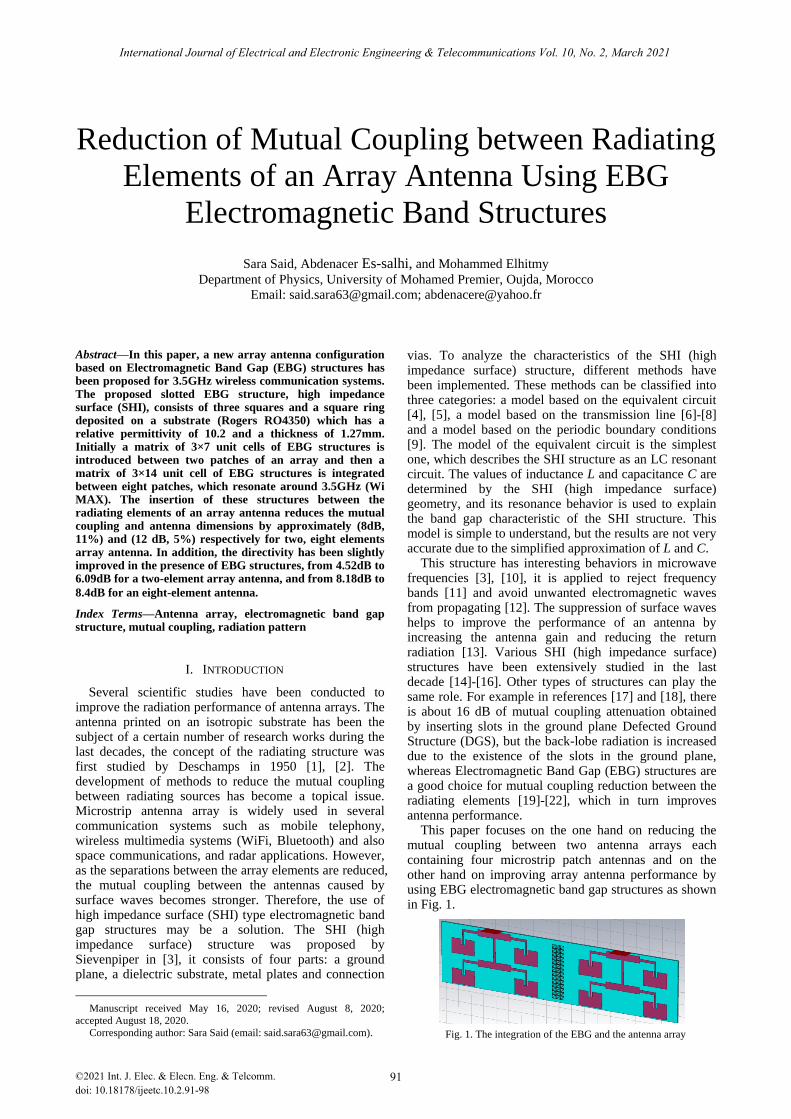
Fig. 19. Array antenna radiation pattern: (a) without EBG, (b) With
EBG
(a) (b)
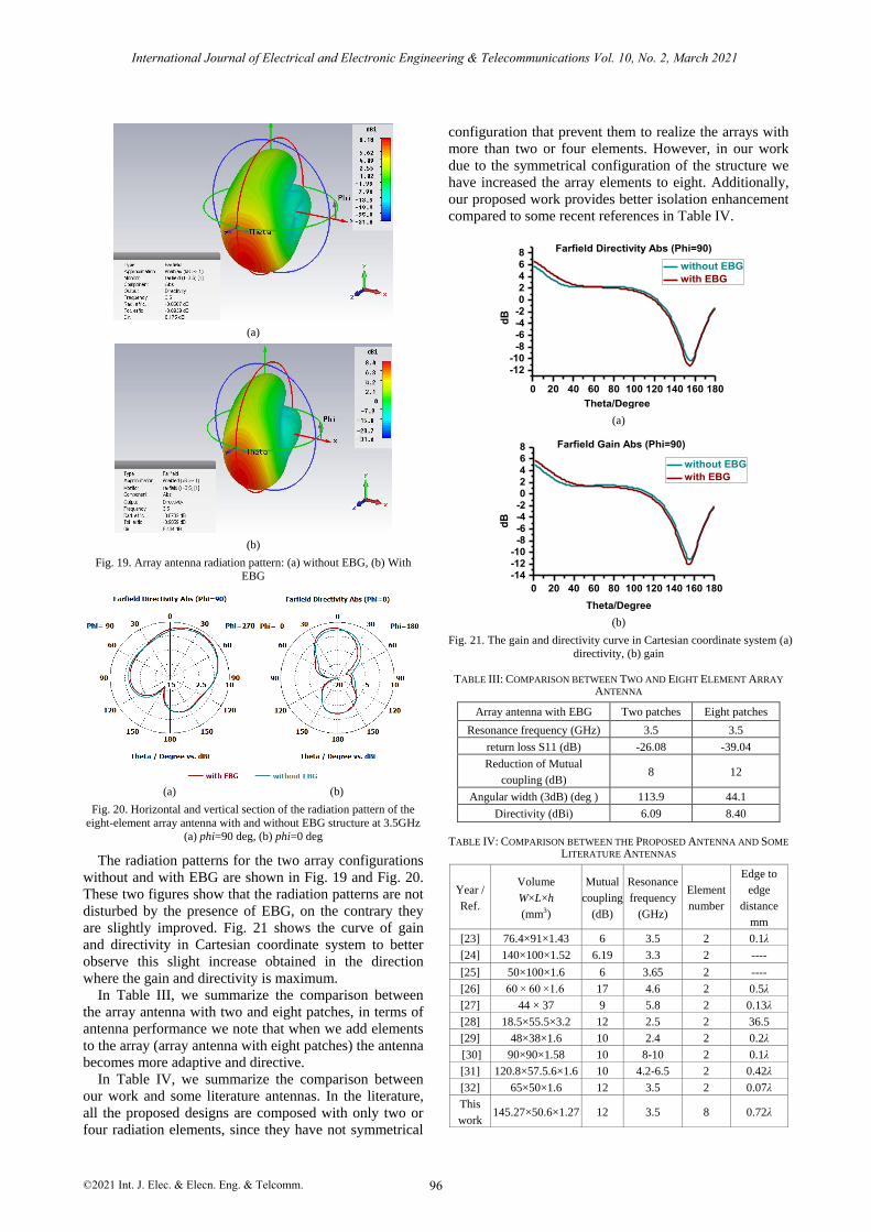
Fig. 20. Horizontal and vertical section of the radiation pattern of the
eight-element array antenna with and without EBG structure at 3.5GHz
(a) phi=90 deg, (b) phi=0 deg
The radiation patterns for the two array configurations
without and with EBG are shown in Fig. 19 and Fig. 20.
These two figures show that the radiation patterns are not
disturbed by the presence of EBG, on the contrary they
are slightly improved. Fig. 21 shows the curve of gain
and directivity in Cartesian coordinate system to better
observe this slight increase obtained in the direction
where the gain and directivity is maximum.
In Table III, we summarize the comparison between
the array antenna with two and eight patches, in terms of
antenna performance we note that when we add elements
to the array (array antenna with eight patches) the antenna
becomes more adaptive and directive.
In Table IV, we summarize the comparison between
our work and some literature antennas. In the literature,
all the proposed designs are composed with only two or
four radiation elements, since they have not symmetrical
configuration that prevent them to realize the arrays with
more than two or four elements. However, in our work
due to the symmetrical configuration of the structure we
have increased the array elements to eight. Additionally,
our proposed work provides better isolation enhancement
compared to some recent references in Table IV.
0 20 40 60 80 100 120 140 160 180
-12-10
-8-6-4-202468
dB
Farfield Directivity Abs (Phi=90)
Theta/Degree
without EBG
with EBG
(a)
0 20 40 60 80 100 120 140 160 180
-14-12-10
-8-6-4-202468
dB
Theta/Degree
Farfield Gain Abs (Phi=90)
dB
without EBG
with EBG
(b)
Fig. 21. The gain and directivity curve in Cartesian coordinate system (a)
directivity, (b) gain
TABLE III: COMPARISON BETWEEN TWO AND EIGHT ELEMENT ARRAY
ANTENNA
Array antenna with EBG Two patches Eight patches
Resonance frequency (GHz) 3.5 3.5
return loss S11 (dB) -26.08 -39.04
Reduction of Mutual
coupling (dB) 8 12
Angular width (3dB) (deg ) 113.9 44.1
Directivity (dBi) 6.09 8.40
TABLE IV: COMPARISON BETWEEN THE PROPOSED ANTENNA AND SOME
LITERATURE ANTENNAS
Year /
Ref.
Volume
W×L×h
(mm3)
Mutual
coupling
(dB)
Resonance
frequency
(GHz)
Element
number
Edge to
edge
distance
mm
[23] 76.4×91×1.43 6 3.5 2 0.1λ
[24] 140×100×1.52 6.19 3.3 2 ----
[25] 50×100×1.6 6 3.65 2 ----
[26] 60 × 60 ×1.6 17 4.6 2 0.5λ
[27] 44 × 37 9 5.8 2 0.13λ
[28] 18.5×55.5×3.2 12 2.5 2 36.5
[29] 48×38×1.6 10 2.4 2 0.2λ
[30] 90×90×1.58 10 8-10 2 0.1λ
[31] 120.8×57.5.6×1.6 10 4.2-6.5 2 0.42λ
[32] 65×50×1.6 12 3.5 2 0.07λ
This
work 145.27×50.6×1.27 12 3.5 8 0.72λ
International Journal of Electrical and Electronic Engineering & Telecommunications Vol. 10, No. 2, March 2021
©2021 Int. J. Elec. & Elecn. Eng. & Telcomm. 96
V. CONCLUSION
In this paper we have shown a very effective aspect of
EBG (Electromagnetic band gap) slotted electromagnetic
band gap structures. These structures play a very
important role, they reduce the coefficient of mutual
coupling between the radiating sources on the one hand,
and on the other hand, they allow to design very low
profile antennas. The insertion of slotted EBG structures
between the radiating elements leads to a reduction in
mutual coupling of around 10 dB compared to the array
antenna without EBG structure, in addition the gain and
directivity are slightly improved. We present here only
the results obtained for d=0.72λ3.5 to 3.5GHz. In
perspective, the proposed antenna will be manufactured
and the simulation results will be validated by the
experimental results.
CONFLICT OF INTEREST
The authors declare no conflict of interest
AUTHOR CONTRIBUTIONS
Author’s contribution to this work: Sara Said and
Abdenacer Es-salhi conducted the research and analyzed
the data; Mohammed Elhitmy corrected the paper
(linguistic correction); all authors had approved the final
version.
REFERENCES
[1] I. J. Bahl and P. Bhartia, Microstrip Antennas, Dedham, Ma:
Artech House, 1980
[2] K. R. Carver and J. W. Mink, “Microstrip antennas technology,”
IEEE Trans. on Antennas and Propagation, vol. 29, no. 1, pp. 2-
24, January 1981.
[3] D. Sievenpiper, L. Zhang, R. F. Broas, N. G. Alexopolous, and E.
Yablonovitch, “High-impedance electromagnetic surfaces with a
forbidden frequency band,” IEEE Trans. on Microwave Theory
and Techniques, vol. 47, no.11, pp. 2059–2074, 1999.
[4] G. K. Pandey, H. S. Singh, P. K. Bharti, and M. K. Meshram,
“Design of WLAN band notched UWB monopole antenna with
stepped geometry using modified EBG structure,” Progress in
Electromagnetic Research B, vol. 50, pp. 201–217, April 2013.
[5] F. Yang and Y. Rahmat-Samii, Electromagnetic Band Gap
Structures in Antenna Engineering, Cambridge University Press
Cambridge, UK, 2009.
[6] L. Yang, M. Fan, F. Chen, J. She, and Z. Feng, “A novel compact
Electromagnetic Band Gap (EBG) structure and its applications
for microwave circuits,” IEEE Trans. on Microwave Theory and
Techniques, vol. 53, no. 1, pp. 183–190, 2005.
[7] L. Li, Q. Chen, Q. Yuan, C. Liang, and K. Sawaya, “Surface-wave
suppression band gap and plane-wave reflection phase band of
mushroom like photonic band gap structures,” Journal of Applied
Physics, vol. 103, no. 2, pp. 023513, 2008.
[8] Z. Iluz, R. Shavit, and R. Bauer, “Microstrip antenna phased array
with electromagnetic band gap substrate,” IEEE Trans. on
Antennas and Propagation, vol. 52, no. 6, pp. 1446–1453, 2004.
[9] Y. Kim, F. Yang, and A. Z. Elsherbeni, “Compact artificial
magnetic conductor designs using planar square spiral
geometries,” Progress in Electromagnetic Research, vol. 77, pp.
43–54, 2007.
[10] F. Yang and Y. Rahmat-Samii, “Reflection phase
characterizations of the EBG ground plane for low profile wire
antenna applications,” IEEE Trans. on Antennas and Propagation,
vol. 51, no. 10, pp. 2691–2703, 2003.
[11] A. Kaabal, S. Ahyoud, and A. Asselman, “A new design of star
antenna for ultra wide band applications with wlan-band-notched
using EBG structures,” Int. J. Microw. Opt. Technol., vol. 9, no. 5,
pp. 544–548, September 2014.
[12] N. H. M. Hanafi, M. T. Islam, and N. Misran, “Analysis of
mushroom-like EBG structure and UC-EBG for SAR reduction,”
in Proc. IEEE Int. Symposium on Antennas and Propagation,
2012, pp. 696–699.
[13] F. Yang and Y. Rahmat-Samii, “Microstrip antennas integrated
with electromagnetic band-gap (EBG) structures: A low mutual
coupling design for array applications,” IEEE Trans. on Antennas
and Propagation, vol. 51, no. 10, pp. 2936–2946, 2003.
[14] N. Kushwaha and R. Kumar, “Study of different shape
Electromagnetic Band Gap (EBG) structures for single and dual
band applications,” Journal of Microwaves, Optoelectronics and
Electromagnetic Applications, vol. 13, no. 1, pp. 16–30, 2014.
[15] Z. Iluz, R. Shavit, and R. Bauer, “Microstrip antenna phased array
with electromagnetic band gap substrate,” IEEE Trans. on
Antennas and Propagation, vol. 52, no. 6, pp. 1446–1453, 2004.
[16] B. Mohajer-Iravani and O. M. Ramahi, “On the suppression band
and band gap of planar electromagnetic band gap structures,” Int.
Journal of Antennas and Propagation, pp. 1-11, January 2014.
[17] A. Habashi, F. Mirzamohamadi, S. Habashi, and J. Nourinia, “A
simple Defected Ground Structure (DGS) for reduction of mutual
coupling in closely spaced microstrip arrays,” J. World’s Electr.
Eng. Technol., vol. 2, pp. 13–16, May 2012.
[18] A. B. Abdel-Rahman, “Coupling reduction of antenna array
elements using small interdigital capacitor loaded slots,” Progress
in Electromagnetics Research C, vol. 27, pp. 15–26, 2012.
[19] A. Ghaloua, J. Zbitou, M. Latrach, L. El Abdellaoui, A. Errkik,
and R. Mandry, “Mutual coupling reduction and miniaturization
arrays antennas using new structure of EBG,” presented at
International Conference on Wireless Technologies, Embedded
and Intelligent Systems, 2017.
[20] A. Arora and N. Kumar, “To reduce mutual coupling in micro
strip patch antenna arrays elements using electromagnetic band
gap structures for X-band,” presented at International Conference
on Nextgen Electronic Technologies: Silicon to Software
(ICNETS2), 2017.
[21] X. Yang, Y. Liu, Y. X. Xu, and S. Gong, “Isolation enhancement
in patch antenna array with fractal UC-EBG structure and cross
slot,” IEEE Antennas and Wireless Propagation Letters, vol. 16,
pp. 2175–2178, May 2017.
[22] A. Kazemipour, “Contribution to the study of coupling between
antennas, application to electromagnetic compatibility and to the
design of antennas and antenna arrays,” PhD thesis, Telecom,
National Higher School of Telecommunications, Paris, 12
December, 2002.
[23] X. M. Yang, X. G. Liu, X. Y. Zhou, and T. J. Cui, “Reduction of
mutual coupling between closely packed patch antennas using
waveguide metamaterials,” IEEE Antennas and Wireless
Propagation Letters, vol. 11, pp. 389–391, April 2012.
[24] F. Y. Zulkifli, E. T Rahardjo, and D. Hartanto, “Mutual coupling
reduction using dumbbell defected ground structure for multiband
microstrip antenna array,” Progress in Electromagnetics Research
Letters, vol. 13, pp. 29–40, 2010.
[25] A. Toktas and A. Akdagli, “Wideband MIMO antenna with
enhanced isolation for LTE, WiMAX and WLAN mobile
handsets,” Electronics Letters, vol. 50, no. 10, pp. 723–72, 2014.
[26] W. Wu, B. Yuan and A. Wu, “A quad-element UWB-MIMO
antenna with band-notch and reduced mutual coupling based on
EBG structures,” Int. Journal of Antennas and Propagation, pp. 1-
10, 2018.
[27] A. Iqbal, O. A Saraereh, A. Bouazizi, and A. Basir,
“Metamaterial-based highly isolated MIMO antenna for portable
wireless applications,” Electronics, vol. 7, no. 10, p. 267, 2018.
[28] K. P. Kumar and H. Khan, “Optimization of electromagnetic band
gap structure for mutual coupling reduction in antenna arrays-A
comparative study,” Int. Journal of Engineering & Technology,
vol. 7, pp. 13-20, 2018.
International Journal of Electrical and Electronic Engineering & Telecommunications Vol. 10, No. 2, March 2021
©2021 Int. J. Elec. & Elecn. Eng. & Telcomm. 97
[29] M. B. Kadu, N. Rayavarapu, and R. P. Labade, “Design of EBG
structure for mutual coupling reduction in patch antenna array,”
presented at International Conference on Advances in
Communication and Computing Technology, 2018.
[30] J. Ghosh and D. Mitra, “A technique for reduction of mutual
coupling by steering surface wave propagation,” Microwave and
Optical Technology Letters, vol. 62, no. 5, pp. 1957-1963, 2020.
[31] O. Sokunbi and H. Attia, “Dual-layer dual-patch EBG structure
for isolation enhancement and correlation reduction in MIMO
antenna arrays,” Progress in Electromagnetics Research C, vol.
100, pp. 233-245, March 2020.
[32] K. S. Vishvaksenan, K. Mithra, R. Kalaiarasan, et al., “Mutual
coupling reduction in microstrip patch antenna arrays using
parallel coupled-line decoupling,” IEEE Antennas and Wireless
Propagation Letters, vol. 16, pp. 2146–2149, 2017.
Copyright © 2021 by the authors. This is an open access article
distributed under the Creative Commons Attribution License (CC BY-
NC-ND 4.0), which permits use, distribution and reproduction in any
medium, provided that the article is properly cited, the use is non-
commercial and no modifications or adaptations are made.
S. Said was born in Oujda, Morocco in 1992. She received the bachelor
and the master degrees in electronics and informatics from University
Mohamed Premier of Oujda (Morocco) in 2013 and 2015 respectively.
She is now pursuing her Ph.D. degree at the Faculty of Sciences of
Oujda. Her interest is designing new antenna topologies based on EBG
materials.
A. Es-salhi Professor of Higher Education, University Mohamed
premier, Faculty of Science, Department of Physics, OUJDA –Morocco.
He received the master degrees (DEA) in Electronic and System from
University Blaise Pascal Clermont Ferrand French in 1986. He received
the first PhD degrees subtitle “Study of the Diffraction of an
Electromagnetic Wave by aperiodic Surfaces. Application to the
calculation of the reinforcement of electromagnetic fields by the surface
of a rough sea”, at University Blaise Pascal Clermont Ferrand French in
1991, the second Phd received at University Mohamed premier, Oujda –
Morocco, subtitle “Coupling of an Electromagnetic Wave to an Aerial
Transmission Line Modeling and Simulation”, in 1996. His teaching
activities: Supervision of projects: Masters DESA, License -
Educational coordinator of the Professional License of Electronics -
Educational coordinator of the Professional License Professional of
Physical and Chemical Science Didactics. His research activities: -
Publications and communications in the fields of Propagation of
electromagnetic waves, transmission lines and antenna radiation-
Supervision of doctoral theses- Director of the laboratory
Electromagnetism signal processing and renewable energy. Now his
interest is in Application of meta-materials to antenna miniaturization
and the realization of ULB ultra wide band antennas, without degrading
the performance of the antenna. (Directivity, gain, bandwidth etc ...).
International Journal of Electrical and Electronic Engineering & Telecommunications Vol. 10, No. 2, March 2021
©2021 Int. J. Elec. & Elecn. Eng. & Telcomm. 98