Embed Size (px)
Citation preview
Reduction of 1/f noise in graphene after electron-beam irradiation
Md. Zahid Hossain,1 Sergey Rumyantsev,2,3 Michael S. Shur,2
and Alexander A. Balandin1,4,a)
1Nano-Device Laboratory, Department of Electrical Engineering, Bourns College of Engineering,University of California–Riverside, Riverside, California 92521, USA2Center for Integrated Electronics and Department of Electrical, Computer, and Systems Engineering,Rensselaer Polytechnic Institute, Troy, New York 12180, USA3Ioffe Physical-Technical Institute, The Russian Academy of Sciences, St. Petersburg 194021, Russia4Materials Science and Engineering Program, University of California–Riverside, Riverside,California 92521, USA
(Received 25 January 2013; accepted 9 April 2013; published online 19 April 2013)
We investigated experimentally the effect of the electron-beam irradiation on the level of the
low-frequency 1/f noise in graphene devices. It was found that 1/f noise in graphene reduces with
increasing concentration of defects induced by irradiation. The increased amount of structural disorder
in graphene under irradiation was verified with micro-Raman spectroscopy. The bombardment of
graphene devices with 20-keV electrons reduced the noise spectral density, SI/I2 (I is the source-drain
current) by an order-of magnitude at the radiation dose of 104 lC/cm2. We analyzed the observed
noise reduction in the limiting cases of the mobility and carrier number fluctuation mechanisms.
The obtained results are important for the proposed graphene applications in analog, mixed-
signal, and radio-frequency systems, integrated circuits and sensors. VC 2013 AIP Publishing LLC[http://dx.doi.org/10.1063/1.4802759]
The level of the flicker 1/f noise1 is one of the key met-
rics that each new material has to pass before it can be used
for practical devices (f is the frequency).2 Graphene3 has
shown a great potential for applications in high-frequency
communications,4,5 analog circuits,6 and sensors.7,8 The
envisioned applications require a low level of 1/f noise,
which contributes to the phase-noise of communication sys-
tems2 and limits the sensor sensitivity.7 Despite significant
research efforts9–15 there is still no conventionally accepted
model for physical mechanisms behind 1/f noise in graphene.
Correspondingly, no comprehensive methods for 1/f noise
suppression in graphene devices have been developed.
In this letter, we show that 1/f noise in graphene reveals
an interesting characteristic—it reduces with increasing con-
centration of defects induced by irradiation. We found that
bombardment of graphene devices with 20-keV electrons
can reduce the noise spectral density, SI/I2 (I is the source-
drain current) by an order-of magnitude at the radiation dose
(RD) of 104 lC/cm2. We analyzed the observed noise reduc-
tion in the framework of the mobility and carrier number
fluctuation mechanisms. We hope that our experimental
results can stimulate a detailed theoretical study of 1/f noise
origin in graphene. Apart from contributing to understanding
the physics behind 1/f noise in graphene, our results can pos-
sibly offer a practical method for noise reduction in various
graphene devices where a trade-off between the noise level
and mobility value is possible.
Graphene revealed a number of unique electronic,3–7
optical,7 and thermal16 properties, which led to proposals of
different graphene-based devices. The high-frequency commu-
nication and analog circuit applications are expected to capital-
ize on high electron mobility and saturation velocity of
graphene.7 The ultimate surface-to-volume ratio and the
Fermi-energy tuning capability make graphene excellent
material for detectors and sensors with demonstrated single-
molecule sensitivity7 and selective gas sensing.8 However, like
with any other new material systems, graphene has to meet the
stringent requirements for the low-frequency 1/f noise level.2
For example, recent development of GaN technology for
radio-frequency and optical communications required substan-
tial decrease of the 1/f noise in this material.2,17
A number of research groups have studied low-
frequency noise in graphene devices.9–15 The noise spectral
density, SI/I2, follows 1/f law but reveals the gate-bias de-
pendence different from that in semiconductor field-effect
transistors.9–15 The noise level was reported to be smaller in
bilayer,9 suspended,13 graded-thickness few-layer, and multi-
layer graphene.14 Other reports pointed out that graphene is
uniquely distinct from metals and semiconductors and a new
framework is necessary to understand 1/f noise near the
zero-carrier density.18–20 Specifically, it was suggested that
the carrier-number fluctuation model is inadequate to under-
stand the zero-carrier density limit in which the conductivity
is proportional not to the carrier density, but to RMS devia-
tions of the carrier density about zero.21 One should note
here that there are many different mechanisms that can con-
tribute to the current fluctuations including charged impur-
ities, non-resonant short-range and resonant defect
scatterers.21–24 In many experimental studies of 1/f noise in
graphene, the interpretations of measured results were differ-
ent. As of today, there is no commonly accepted model of 1/fnoise in graphene, which could be used for various gating
and environmental conditions. We undertook the present
investigation considering that the irradiation experiments
were crucial for gaining understanding 1/f noise in conven-
tional materials and metal-oxide-semiconductor field-effect
transistors.25–27 The study of the effects produced by the
a)Author to whom correspondence should be addressed. Electronic mail:
0003-6951/2013/102(15)/153512/5/$30.00 VC 2013 AIP Publishing LLC102, 153512-1
APPLIED PHYSICS LETTERS 102, 153512 (2013)
electron beams on 1/f noise in graphene can elucidate the
mechanisms of 1/f noise and answer a question of graphene’s
prospects for radiation-hard applications.
Graphene is relatively susceptible to the electron and
ion bombardment owing to its single-atom thickness.28–30
Electron irradiation can introduce different types of defects
in graphene depending on the beam energy and local envi-
ronment, e.g., the presence of organic contaminants. For this
study, we selected the electron energy of 20 keV in order to
exclude the severe knock-on damage to the graphene crystal
lattice, which starts at �50 keV.30 The back-gated graphene
devices were fabricated using mechanical exfoliation5 and
standard lithographic fabrication techniques.10,14 The num-
ber of atomic planes and absence of defects in pristine gra-
phene have been checked with Raman spectroscopy. The
devices were subjected to the electron-beam irradiation in
the scanning-electron microscopy (SEM) chamber of the
electron-beam lithography (EBL) system under high-vacuum
conditions. The following testing protocol was applied. The
Raman spectrum and 1/f noise were measured for all devices
before irradiation. The graphene channels were then exposed
to the first RD followed by the Raman spectroscopy and
noise measurements. The process was repeated several times
until the total RD reached 105 lC/cm2.
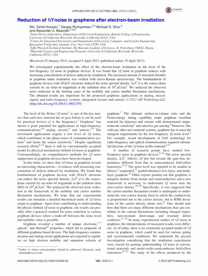
Figure 1(a) shows a SEM image of a graphene channel
with four metal contacts, while Figure 1(b) illustrates the area
of graphene between two contacts subjected to irradiation.
The Raman spectrum of graphene before and after irradiation
with RD¼ 104 lC/cm2 is presented in Figure 1(c). One can
see the appearance of the strong disorder D and D0 peaks after
irradiation indicating that electron bombardment introduced
defects to graphene.29 The strength of the irradiation effects
can be deduced from the intensity ratio, I(D)/I(G), presented
in Figure 1(d). I(D)/I(G) increases monotonically with RD in
the range of interest. Defect introduction results in correspond-
ing asymmetric broadening of 2D band, which can also be
used to monitor defects introduction (see inset in Figure 1(d)).
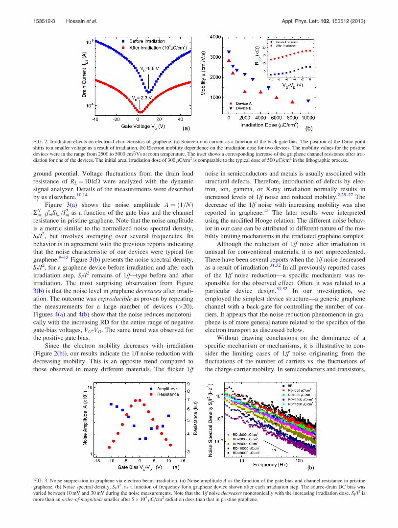
The electrical conduction properties of graphene under
irradiation evolved as we expected. The electron bombard-
ment led to a shift in the Dirac point position and decrease in
mobility, l, with the corresponding increase in the source-
drain resistance, RSD. The initial position of the Dirac point
(VD� 10 V) is typical for as-fabricated devices owing to the
background doping from water moisture or resist residues
from lithographic processes. The Dirac point shifted to �2 V
after exposure to RD¼ 104 lC/cm2 (Figure 2(a)). Such a
behavior was observed for most devices, although in a very
few cases, we recorded a positive shift of the Dirac point af-
ter some irradiation steps. The mobility decreases with
increasing RD but remains acceptable from the applications
point of view (Figure 2(b)). The low-frequency noise meas-
urements were performed using the in-house built setup
shielded inside a metal enclosure. The noise was measured
in the linear region of the drain bias keeping the source at a
FIG. 1. Graphene device irradiation with electron beams. (a) SEM image of graphene devices with multiple metal contacts. The dark ribbons are graphene
channels while the white regions are Ti/Au(10-nm/90-nm) electrodes. The scale bar is 2 lm. (b) Schematic of the irradiation process showing the area exposed
to the electron beam. The whole area between the metal contacts is irradiated. (c) Raman spectrum of graphene before and after irradiation. The single-layer
graphene signatures include G peak at �1584 cm�1 and symmetric 2D band at �2692 cm�1. The absence of the disorder D peak at �1350 cm�1 proves that
graphene is high quality and defect-free before irradiation. Appearance of the disorder D and D0 peaks after irradiation indicates that electron bombardment
introduced defects to graphene. (d) Intensity ratio I(D)/I(G) as a function of the irradiation dose. The inset shows the normalized 2D band at different irradia-
tion doses shifted in energy to the same position for the ease of comparison. Note the asymmetric broadening and skewing toward the lower wave numbers.
The full-width at half maximum of 2D band before irradiation was �28 cm�1 while after irradiation it increased to �36 cm�1 at the irradiation dose of
5� 104 lC/cm2.
153512-2 Hossain et al. Appl. Phys. Lett. 102, 153512 (2013)
ground potential. Voltage fluctuations from the drain load
resistance of RL¼ 10 kX were analyzed with the dynamic
signal analyzer. Details of the measurements were described
by us elsewhere.10,14
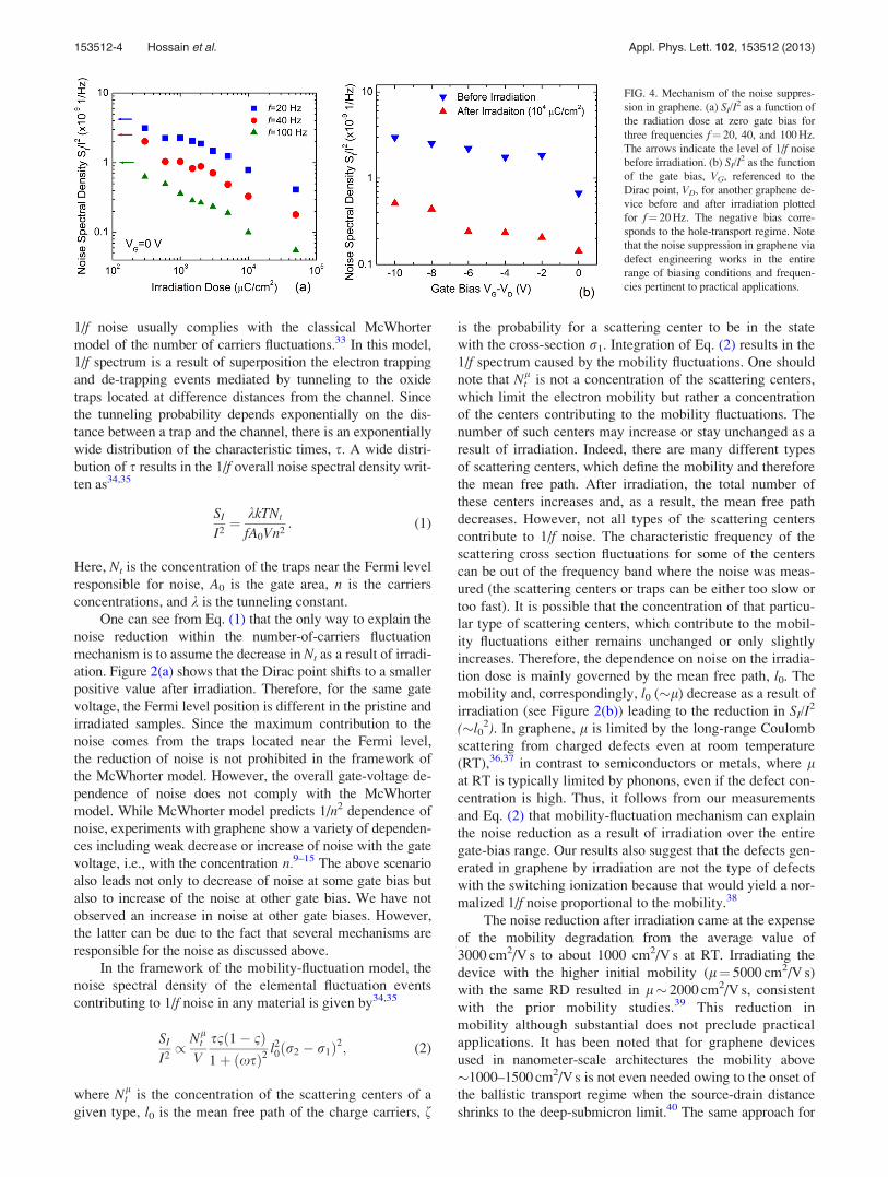
Figure 3(a) shows the noise amplitude A ¼ ð1=NÞRN
m¼1fmSIm=I2
m as a function of the gate bias and the channel
resistance in pristine graphene. Note that the noise amplitude
is a metric similar to the normalized noise spectral density,
SI/I2, but involves averaging over several frequencies. Its
behavior is in agreement with the previous reports indicating
that the noise characteristic of our devices were typical for
graphene.9–15 Figure 3(b) presents the noise spectral density,
SI/I2, for a graphene device before irradiation and after each
irradiation step. SI/I2 remains of 1/f—type before and after
irradiation. The most surprising observation from Figure
3(b) is that the noise level in graphene decreases after irradi-
ation. The outcome was reproducible as proven by repeating
the measurements for a large number of devices (>20).
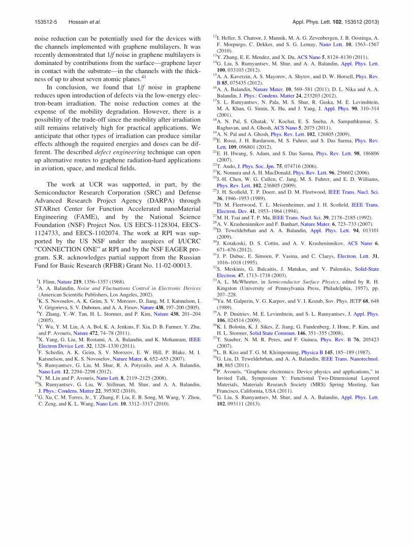
Figures 4(a) and 4(b) show that the noise reduces monotoni-
cally with the increasing RD for the entire range of negative
gate-bias voltages, VG-VD. The same trend was observed for
the positive gate bias.
Since the electron mobility decreases with irradiation
(Figure 2(b)), our results indicate the 1/f noise reduction with
decreasing mobility. This is an opposite trend compared to
those observed in many different materials. The flicker 1/f
noise in semiconductors and metals is usually associated with
structural defects. Therefore, introduction of defects by elec-
tron, ion, gamma, or X-ray irradiation normally results in
increased levels of 1/f noise and reduced mobility.2,25–27 The
decrease of the 1/f noise with increasing mobility was also
reported in graphene.13 The later results were interpreted
using the modified Hooge relation. The different noise behav-
ior in our case can be attributed to different nature of the mo-
bility limiting mechanisms in the irradiated graphene samples.
Although the reduction of 1/f noise after irradiation is
unusual for conventional materials, it is not unprecedented.
There have been several reports when the 1/f noise decreased
as a result of irradiation.31,32 In all previously reported cases
of the 1/f noise reduction—a specific mechanism was re-
sponsible for the observed effect. Often, it was related to a
particular device design.31,32 In our investigation, we
employed the simplest device structure—a generic graphene
channel with a back-gate for controlling the number of car-
riers. It appears that the noise reduction phenomenon in gra-
phene is of more general nature related to the specifics of the
electron transport as discussed below.
Without drawing conclusions on the dominance of a
specific mechanism or mechanisms, it is illustrative to con-
sider the limiting cases of 1/f noise originating from the
fluctuations of the number of carriers vs. the fluctuations of
the charge-carrier mobility. In semiconductors and transistors,
FIG. 3. Noise suppression in graphene via electron beam irradiation. (a) Noise amplitude A as the function of the gate bias and channel resistance in pristine
graphene. (b) Noise spectral density, SI/I2, as a function of frequency for a graphene device shown after each irradiation step. The source-drain DC bias was
varied between 10 mV and 30 mV during the noise measurements. Note that the 1/f noise decreases monotonically with the increasing irradiation dose. SI/I2 is
more than an order-of-magnitude smaller after 5� 104 lC/cm2 radiation does than that in pristine graphene.
FIG. 2. Irradiation effects on electrical characteristics of graphene. (a) Source-drain current as a function of the back-gate bias. The position of the Dirac point
shifts to a smaller voltage as a result of irradiation. (b) Electron mobility dependence on the irradiation dose for two devices. The mobility values for the pristine
devices were in the range from 2500 to 5000 cm2/Vs at room temperature. The inset shows a corresponding increase of the graphene channel resistance after irra-
diation for one of the devices. The initial areal irradiation dose of 300 lC/cm2 is comparable to the typical dose of 500 lC/cm2 in the lithographic process.
153512-3 Hossain et al. Appl. Phys. Lett. 102, 153512 (2013)
1/f noise usually complies with the classical McWhorter
model of the number of carriers fluctuations.33 In this model,
1/f spectrum is a result of superposition the electron trapping
and de-trapping events mediated by tunneling to the oxide
traps located at difference distances from the channel. Since
the tunneling probability depends exponentially on the dis-
tance between a trap and the channel, there is an exponentially
wide distribution of the characteristic times, s. A wide distri-
bution of s results in the 1/f overall noise spectral density writ-
ten as34,35
SI
I2¼ kkTNt
fA0Vn2: (1)
Here, Nt is the concentration of the traps near the Fermi level
responsible for noise, A0 is the gate area, n is the carriers
concentrations, and k is the tunneling constant.
One can see from Eq. (1) that the only way to explain the
noise reduction within the number-of-carriers fluctuation
mechanism is to assume the decrease in Nt as a result of irradi-
ation. Figure 2(a) shows that the Dirac point shifts to a smaller
positive value after irradiation. Therefore, for the same gate
voltage, the Fermi level position is different in the pristine and
irradiated samples. Since the maximum contribution to the
noise comes from the traps located near the Fermi level,
the reduction of noise is not prohibited in the framework of
the McWhorter model. However, the overall gate-voltage de-
pendence of noise does not comply with the McWhorter
model. While McWhorter model predicts 1/n2 dependence of
noise, experiments with graphene show a variety of dependen-
ces including weak decrease or increase of noise with the gate
voltage, i.e., with the concentration n.9–15 The above scenario
also leads not only to decrease of noise at some gate bias but
also to increase of the noise at other gate bias. We have not
observed an increase in noise at other gate biases. However,
the latter can be due to the fact that several mechanisms are
responsible for the noise as discussed above.
In the framework of the mobility-fluctuation model, the
noise spectral density of the elemental fluctuation events
contributing to 1/f noise in any material is given by34,35
SI
I2/ Nl
t
V
s1ð1� 1Þ1þ ðxsÞ2
l20ðr2 � r1Þ2; (2)
where Nlt is the concentration of the scattering centers of a
given type, l0 is the mean free path of the charge carriers, f
is the probability for a scattering center to be in the state
with the cross-section r1. Integration of Eq. (2) results in the
1/f spectrum caused by the mobility fluctuations. One should
note that Nlt is not a concentration of the scattering centers,
which limit the electron mobility but rather a concentration
of the centers contributing to the mobility fluctuations. The
number of such centers may increase or stay unchanged as a
result of irradiation. Indeed, there are many different types
of scattering centers, which define the mobility and therefore
the mean free path. After irradiation, the total number of
these centers increases and, as a result, the mean free path
decreases. However, not all types of the scattering centers
contribute to 1/f noise. The characteristic frequency of the
scattering cross section fluctuations for some of the centers
can be out of the frequency band where the noise was meas-
ured (the scattering centers or traps can be either too slow or
too fast). It is possible that the concentration of that particu-
lar type of scattering centers, which contribute to the mobil-
ity fluctuations either remains unchanged or only slightly
increases. Therefore, the dependence on noise on the irradia-
tion dose is mainly governed by the mean free path, l0. The
mobility and, correspondingly, l0 (�l) decrease as a result of
irradiation (see Figure 2(b)) leading to the reduction in SI/I2
(�l02). In graphene, l is limited by the long-range Coulomb
scattering from charged defects even at room temperature
(RT),36,37 in contrast to semiconductors or metals, where lat RT is typically limited by phonons, even if the defect con-
centration is high. Thus, it follows from our measurements
and Eq. (2) that mobility-fluctuation mechanism can explain
the noise reduction as a result of irradiation over the entire
gate-bias range. Our results also suggest that the defects gen-
erated in graphene by irradiation are not the type of defects
with the switching ionization because that would yield a nor-
malized 1/f noise proportional to the mobility.38
The noise reduction after irradiation came at the expense
of the mobility degradation from the average value of
3000 cm2/V s to about 1000 cm2/V s at RT. Irradiating the
device with the higher initial mobility (l¼ 5000 cm2/V s)
with the same RD resulted in l� 2000 cm2/V s, consistent
with the prior mobility studies.39 This reduction in
mobility although substantial does not preclude practical
applications. It has been noted that for graphene devices
used in nanometer-scale architectures the mobility above
�1000–1500 cm2/V s is not even needed owing to the onset of
the ballistic transport regime when the source-drain distance
shrinks to the deep-submicron limit.40 The same approach for
FIG. 4. Mechanism of the noise suppres-
sion in graphene. (a) SI/I2 as a function of
the radiation dose at zero gate bias for
three frequencies f¼ 20, 40, and 100 Hz.
The arrows indicate the level of 1/f noise
before irradiation. (b) SI/I2 as the function
of the gate bias, VG, referenced to the
Dirac point, VD, for another graphene de-
vice before and after irradiation plotted
for f¼ 20 Hz. The negative bias corre-
sponds to the hole-transport regime. Note
that the noise suppression in graphene via
defect engineering works in the entire
range of biasing conditions and frequen-
cies pertinent to practical applications.
153512-4 Hossain et al. Appl. Phys. Lett. 102, 153512 (2013)
noise reduction can be potentially used for the devices with
the channels implemented with graphene multilayers. It was
recently demonstrated that 1/f noise in graphene multilayers is
dominated by contributions from the surface—graphene layer
in contact with the substrate—in the channels with the thick-
ness of up to about seven atomic planes.41
In conclusion, we found that 1/f noise in graphene
reduces upon introduction of defects via the low-energy elec-
tron-beam irradiation. The noise reduction comes at the
expense of the mobility degradation. However, there is a
possibility of the trade-off since the mobility after irradiation
still remains relatively high for practical applications. We
anticipate that other types of irradiation can produce similar
effects although the required energies and doses can be dif-
ferent. The described defect engineering technique can open
up alternative routes to graphene radiation-hard applications
in aviation, space, and medical fields.
The work at UCR was supported, in part, by the
Semiconductor Research Corporation (SRC) and Defense
Advanced Research Project Agency (DARPA) through
STARnet Center for Function Accelerated nanoMaterial
Engineering (FAME), and by the National Science
Foundation (NSF) Project Nos. US EECS-1128304, EECS-
1124733, and EECS-1102074. The work at RPI was sup-
ported by the US NSF under the auspices of I/UCRC
“CONNECTION ONE” at RPI and by the NSF EAGER pro-
gram. S.R. acknowledges partial support from the Russian
Fund for Basic Research (RFBR) Grant No. 11-02-00013.
1I. Flinn, Nature 219, 1356–1357 (1968).2A. A. Balandin, Noise and Fluctuations Control in Electronic Devices(American Scientific Publishers, Los Angeles, 2002).
3K. S. Novoselov, A. K. Geim, S. V. Morozov, D. Jiang, M. I. Katsnelson, I.
V. Grigorieva, S. V. Dubonos, and A. A. Firsov, Nature 438, 197–200 (2005).4Y. Zhang, Y.-W. Tan, H. L. Stormer, and P. Kim, Nature 438, 201–204
(2005).5Y. Wu, Y. M. Lin, A. A. Bol, K. A. Jenkins, F. Xia, D. B. Farmer, Y. Zhu,
and P. Avouris, Nature 472, 74–78 (2011).6X. Yang, G. Liu, M. Rostami, A. A. Balandin, and K. Mohanram, IEEE
Electron Device Lett. 32, 1328–1330 (2011).7F. Schedin, A. K. Geim, S. V. Morozov, E. W. Hill, P. Blake, M. I.
Katsnelson, and K. S. Novoselov, Nature Mater. 6, 652–655 (2007).8S. Rumyantsev, G. Liu, M. Shur, R. A. Potyrailo, and A. A. Balandin,
Nano Lett. 12, 2294–2298 (2012).9Y. M. Lin and P. Avouris, Nano Lett. 8, 2119–2125 (2008).
10S. Rumyantsev, G. Liu, W. Stillman, M. Shur, and A. A. Balandin,
J. Phys.: Condens. Matter 22, 395302 (2010).11G. Xu, C. M. Torres, Jr., Y. Zhang, F. Liu, E. B. Song, M. Wang, Y. Zhou,
C. Zeng, and K. L. Wang, Nano Lett. 10, 3312–3317 (2010).
12I. Heller, S. Chatoor, J. Mannik, M. A. G. Zevenbergen, J. B. Oostinga, A.
F. Morpurgo, C. Dekker, and S. G. Lemay, Nano Lett. 10, 1563–1567
(2010).13Y. Zhang, E. E. Mendez, and X. Du, ACS Nano 5, 8124–8130 (2011).14G. Liu, S. Rumyantsev, M. Shur, and A. A. Balandin, Appl. Phys. Lett.
100, 033103 (2012).15A. A. Kaverzin, A. S. Mayorov, A. Shytov, and D. W. Horsell, Phys. Rev.
B 85, 075435 (2012).16A. A. Balandin, Nature Mater. 10, 569–581 (2011); D. L. Nika and A. A.
Balandin, J. Phys.: Condens. Matter 24, 233203 (2012).17S. L. Rumyantsev, N. Pala, M. S. Shur, R. Gaska, M. E. Levinshtein,
M. A. Khan, G. Simin, X. Hu, and J. Yang, J. Appl. Phys. 90, 310–314
(2001).18A. N. Pal, S. Ghatak, V. Kochat, E. S. Sneha, A. Sampathkumar, S.
Raghavan, and A. Ghosh, ACS Nano 5, 2075 (2011).19A. N. Pal and A. Ghosh, Phys. Rev. Lett. 102, 126805 (2009).20E. Rossi, J. H. Bardarson, M. S. Fuhrer, and S. Das Sarma, Phys. Rev.
Lett. 109, 096801 (2012).21E. H. Hwang, S. Adam, and S. Das Sarma, Phys. Rev. Lett. 98, 186806
(2007).22T. Ando, J. Phys. Soc. Jpn. 75, 074716 (2006).23K. Nomura and A. H. MacDonald, Phys. Rev. Lett. 96, 256602 (2006).24J.-H. Chen, W. G. Cullen, C. Jang, M. S. Fuhrer, and E. D. Williams,
Phys. Rev. Lett. 102, 236805 (2009).25J. H. Scofield, T. P. Doerr, and D. M. Fleetwood, IEEE Trans. Nucl. Sci.
36, 1946–1953 (1989).26D. M. Fleetwood, T. L. Meisenheimer, and J. H. Scofield, IEEE Trans.
Electron. Dev. 41, 1953–1964 (1994).27M. H. Tsai and T. P. Ma, IEEE Trans. Nucl. Sci. 39, 2178–2185 (1992).28A. V. Krasheninnikov and F. Banhart, Nature Mater. 6, 723–733 (2007).29D. Teweldebrhan and A. A. Balandin, Appl. Phys. Lett. 94, 013101
(2009).30J. Kotakoski, D. S. Cottin, and A. V. Krasheninnikov, ACS Nano 6,
671–676 (2012).31J. P. Dubuc, E. Simoen, P. Vasina, and C. Claeys, Electron. Lett. 31,
1016–1018 (1995).32S. Meskinis, G. Balcaitis, J. Matukas, and V. Palenskis, Solid-State
Electron. 47, 1713–1718 (2003).33A. L. McWhorter, in Semiconductor Surface Physics, edited by R. H.
Kingston (University of Pennsylvania Press, Philadelphia, 1957), pp.
207–228.34Yu. M. Galperin, V. G. Karpov, and V. I. Kozub, Sov. Phys. JETP 68, 648
(1989).35A. P. Dmitriev, M. E. Levinshtein, and S. L. Rumyantsev, J. Appl. Phys.
106, 024514 (2009).36K. I. Bolotin, K. J. Sikes, Z. Jiang, G. Fundenberg, J. Hone, P. Kim, and
H. L. Stormer, Solid State Commun. 146, 351–355 (2008).37T. Stauber, N. M. R. Peres, and F. Guinea, Phys. Rev. B 76, 205423
(2007).38L. B. Kiss and T. G. M. Kleinpenning, Physica B 145, 185–189 (1987).39G. Liu, D. Teweldebrhan, and A. A. Balandin, IEEE Trans. Nanotechnol.
10, 865 (2011).40P. Avouris, “Graphene electronics: Device physics and applications,” in
Invited Talk, Symposium Y: Functional Two-Dimensional Layered
Materials, Materials Research Society (MRS) Spring Meeting, San
Francisco, California, USA (2011).41G. Liu, S. Rumyantsev, M. Shur, and A. A. Balandin, Appl. Phys. Lett.
102, 093111 (2013).
153512-5 Hossain et al. Appl. Phys. Lett. 102, 153512 (2013)


![Electron–Phonon Coupling in Two-Dimensional ...tion driven superconductivity in doped graphene [49] due to the very low electron– phonon coupling in graphene. Indeed, conventional](https://img.pdfslide.us/doc/110x75/613331aadfd10f4dd73aee43/electronaphonon-coupling-in-two-dimensional-tion-driven-superconductivity.jpg)