Embed Size (px)
Citation preview

Tunnelling and noise in GaAs and graphene
nanostructures
Submitted by Alexander S. Mayorov to the University of Exeter as a
thesis for the degree of Doctor of Philosophy in Physics
September, 2008
This thesis is available for Library use on the understanding that it is copyright
material and that no quotation from the thesis may be published without proper
acknowledgement.
I certify that all material in this thesis which is not my own work has been
identified and that no material has previously been submitted and approved for the
award of a degree by this or any other University.
Alexander S. Mayorov
September, 2008
1

Abstract
Experimental studies presented in this thesis have shown the first realisation of
resonant tunnelling transport through two impurities in a vertical double-barrier
tunnelling diode; have proved the chiral nature of charge carriers in graphene by
studying ballistic transport through graphene p-n junctions; have demonstrated
significant differences of 1/f noise in graphene compared with conventional two-
dimensional systems.
Magnetic field parallel to the current has been used to investigate resonant tun-
nelling through a double impurity in a vertical double-barrier resonant tunnelling
diode, by measuring the current-voltage and differential conductance-voltage char-
acteristics of the structure. It is shown that such experiments allow one to obtain
the energy levels, the effective electron mass and spatial positions of the impurities.
The chiral nature of the carriers in graphene has been demonstrated by com-
paring measurements of the conductance of a graphene p-n-p structure with the
predictions of diffusive models. This allowed us to find, unambiguously, the con-
tribution of ballistic resistance of graphene p-n junctions to the total resistance of
the p-n-p structure. In order to do this, the band profile of the p-n-p structure has
been calculated using the realistic density of states in graphene. It has been shown
that the developed models of diffusive transport can be applied to explain the main
features of the magnetoresistance of p-n-p structures.
It was shown that 1/f noise in graphene has much more complicated concen-
tration and temperature dependences near the Dirac point than in usual metallic
systems, possibly due to the existence of the electron-hole puddles in the electro-
neutrality region. In the regions of high carrier concentration where no inhomogene-
ity is expected, the noise has an inverse square root dependence on the concentration,
which is also in contradiction with the Hooge relation.
2

Acknowledgements
I would like here to say thank you to several people who helped me during
my years of research at the university of Exeter. Firstly to my supervisor Alex
Savchenko, for his encouragement and support. A lot of thanks also go to the PhD
students I worked with: Evgeniy Galaktionov, Fedor Tikhonenko. Special thanks to
Adam Price who corrected my English and David Horsell who read this thesis and
spent a lot of time to make it clearer. Great thanks go to Andrew Kretinin from
whom I learned how to measure noise.
The DBRTD sample was supplied by Giancarlo Faini of the Laboratoire de Pho-
tonique et Nanostructures, CNRS in Marcoussis, France. I am grateful to Roman
Gorbachev who fabricated all graphene samples I have used. Also I want to thank
Alex Beaton who helped me with the graphene doping experiment.
Thanks to theoreticians Matvey Entin from the Institute of Semiconductor
Physics, Novosibirsk, Russia and Francisco Guinea from Instituto de Ciencia de
Materiales de Madrid, Spain, who helped me to get a better understanding of the
physics I was dealing with. Also I would like to express my gratitude to Professor
Kvon Ze Don from the Institute of Semiconductor Physics, Novosibirsk with whom
I worked for a month. He was also the one who told me about Exeter university,
and the ORS scholarship.
I would like to thank all the technical staff in the Physics Department who
helped me, especially Dave Manning and Adam Woodgate for their generous supply
of liquid helium, and Paul Wilkins for solving all my technical problems.
Finally, I owe a big thank you to my mother Tat’yana, and to my sister Maria
for support over the last years. Thanks to my friends Alexey Petrenko and Anatoly
Patrakov who were not here but helped me a lot. I would like to thanks Mr. and
Mrs. Allison who ensured that I did not have any problem with my accommodation
during my PhD study.
Thanks also to all the people I have interacted with during my PhD study at
Exeter but did not mention here.
3

Contents
Abstract 2
Acknowledgements 3
Contents 4
List of Figures 8
List of Tables 18
List of publications 19
Introduction 21
1 Basic concepts 24
1.1 Introduction . . . . . . . . . . . . . . . . . . . . . . . . . . . . . . . . 24
1.2 Low-dimensional systems . . . . . . . . . . . . . . . . . . . . . . . . . 24
1.2.1 Two-dimensional electron gas . . . . . . . . . . . . . . . . . . 24
1.2.2 The Boltzmann equation . . . . . . . . . . . . . . . . . . . . . 27
1.2.3 Landauer-Buttiker approach . . . . . . . . . . . . . . . . . . . 29
1.2.4 Quantum dots and shallow donors in GaAs . . . . . . . . . . . 31
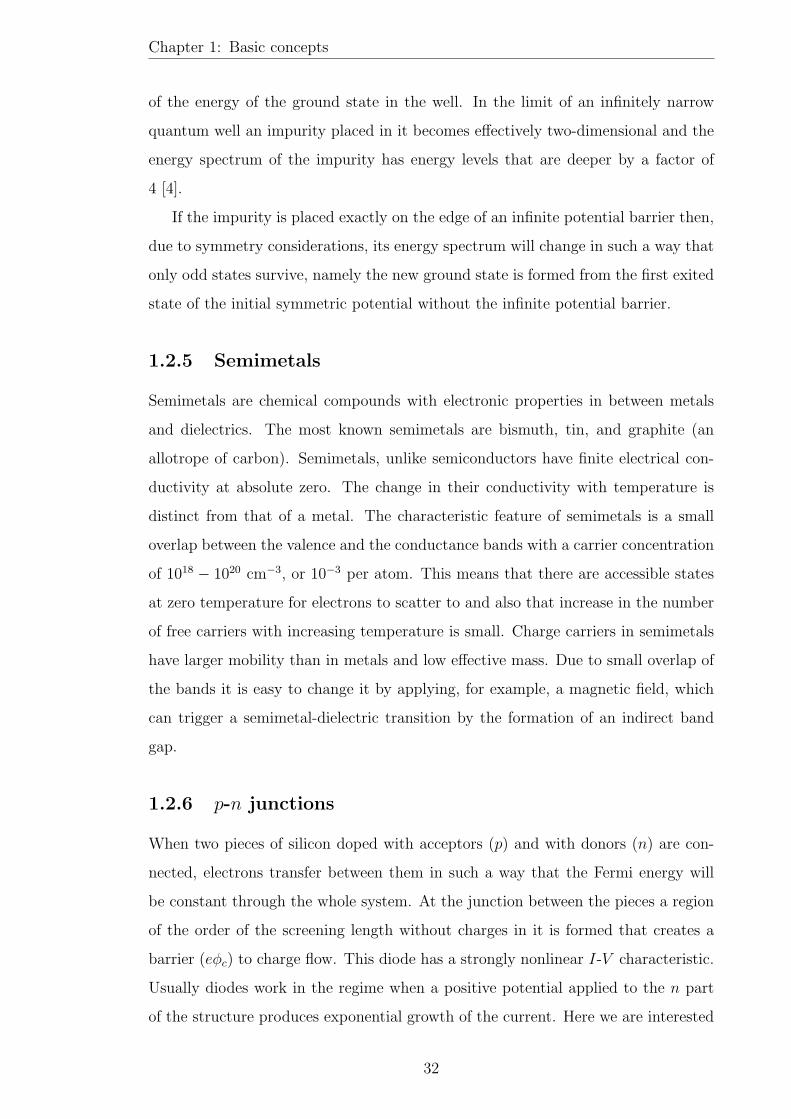
1.2.5 Semimetals . . . . . . . . . . . . . . . . . . . . . . . . . . . . 32
1.2.6 p-n junctions . . . . . . . . . . . . . . . . . . . . . . . . . . . 32
1.2.7 Resonant tunnelling diode . . . . . . . . . . . . . . . . . . . . 33
1.3 Basics of noise . . . . . . . . . . . . . . . . . . . . . . . . . . . . . . . 35
1.3.1 General noise characteristics . . . . . . . . . . . . . . . . . . . 35
1.3.2 Thermal noise . . . . . . . . . . . . . . . . . . . . . . . . . . . 38
1.3.3 Random telegraph noise . . . . . . . . . . . . . . . . . . . . . 38
4

CONTENTS
1.3.4 1/f noise or flicker noise . . . . . . . . . . . . . . . . . . . . . 39
1.3.5 Shot noise . . . . . . . . . . . . . . . . . . . . . . . . . . . . . 40
2 Samples and experimental techniques 42
2.1 Introduction . . . . . . . . . . . . . . . . . . . . . . . . . . . . . . . . 42
2.2 Samples . . . . . . . . . . . . . . . . . . . . . . . . . . . . . . . . . . 42
2.2.1 Double barrier resonant tunnelling diode . . . . . . . . . . . . 42
2.2.2 Graphene samples for noise measurements . . . . . . . . . . . 44
2.2.3 Graphene p-n-p samples . . . . . . . . . . . . . . . . . . . . . 48
2.3 Circuitry and methods . . . . . . . . . . . . . . . . . . . . . . . . . . 49
2.3.1 I-V characteristics . . . . . . . . . . . . . . . . . . . . . . . . 49
2.3.2 Resistance measurements . . . . . . . . . . . . . . . . . . . . . 49
2.3.3 Noise . . . . . . . . . . . . . . . . . . . . . . . . . . . . . . . . 51
2.3.4 Temperature and magnetic field control . . . . . . . . . . . . . 51
3 Transport through impurities in a vertical double-barrier resonant
tunnelling diode 54
3.1 Introduction . . . . . . . . . . . . . . . . . . . . . . . . . . . . . . . . 54
3.2 Theory of resonant tunnelling . . . . . . . . . . . . . . . . . . . . . . 55
3.2.1 Resonant tunnelling via a quantum well in a DBRTD . . . . . 55
3.2.2 Tunnelling through one impurity . . . . . . . . . . . . . . . . 55
3.2.3 Tunnelling through two states . . . . . . . . . . . . . . . . . . 57
3.2.4 Effect of magnetic field . . . . . . . . . . . . . . . . . . . . . . 59
3.3 Experiment and analysis . . . . . . . . . . . . . . . . . . . . . . . . . 62
3.3.1 General I-V characteristic of DBRTD . . . . . . . . . . . . . . 62
3.3.2 Random telegraph noise in DBRTD at 4.2 K . . . . . . . . . . 62
3.3.3 I-V characteristics at T=0.25 K . . . . . . . . . . . . . . . . . 64
3.3.4 Effect of magnetic field on the current peak . . . . . . . . . . 69
3.3.5 Analysis of the current peak in the presence of magnetic field . 72
3.3.6 Diamagnetic shift and current amplitude . . . . . . . . . . . . 74
3.4 Conclusions . . . . . . . . . . . . . . . . . . . . . . . . . . . . . . . . 77
4 Charge carrier transport in graphene 78
4.1 Introduction . . . . . . . . . . . . . . . . . . . . . . . . . . . . . . . . 78
5

CONTENTS
4.2 Graphene . . . . . . . . . . . . . . . . . . . . . . . . . . . . . . . . . 79
4.2.1 Crystal lattice . . . . . . . . . . . . . . . . . . . . . . . . . . . 80
4.2.2 Band structure . . . . . . . . . . . . . . . . . . . . . . . . . . 81
4.2.3 Effective Dirac equation . . . . . . . . . . . . . . . . . . . . . 83
4.2.4 Rotation . . . . . . . . . . . . . . . . . . . . . . . . . . . . . . 85
4.2.5 Chirality . . . . . . . . . . . . . . . . . . . . . . . . . . . . . . 86
4.3 Transport properties . . . . . . . . . . . . . . . . . . . . . . . . . . . 86
4.3.1 p-n junction . . . . . . . . . . . . . . . . . . . . . . . . . . . . 89
4.3.2 Ballistic transport in a p-n junction . . . . . . . . . . . . . . . 90
4.3.3 Ballistic transport in a p-n-p junction . . . . . . . . . . . . . . 92
4.4 Experiment and analysis . . . . . . . . . . . . . . . . . . . . . . . . . 95
4.4.1 Overview of the experimental results . . . . . . . . . . . . . . 95
4.4.2 Electrostatic model . . . . . . . . . . . . . . . . . . . . . . . . 100
4.4.3 p-n junction . . . . . . . . . . . . . . . . . . . . . . . . . . . . 104
4.4.4 p-n-p junction . . . . . . . . . . . . . . . . . . . . . . . . . . . 107
4.4.5 Magnetoresistance of p-n-p structure . . . . . . . . . . . . . . 108
4.5 Conclusions . . . . . . . . . . . . . . . . . . . . . . . . . . . . . . . . 110
5 Noise in graphene 112
5.1 Introduction . . . . . . . . . . . . . . . . . . . . . . . . . . . . . . . . 112
5.2 Noise in conventional systems . . . . . . . . . . . . . . . . . . . . . . 112
5.2.1 1/f noise in MOSFETs . . . . . . . . . . . . . . . . . . . . . . 113
5.2.2 1/f noise in carbon nanotubes . . . . . . . . . . . . . . . . . . 116
5.2.3 Experiments on 1/f noise in graphene nanoribbons . . . . . . 116
5.3 Experiments and analysis . . . . . . . . . . . . . . . . . . . . . . . . 117
5.3.1 1/f noise in multilayer graphene . . . . . . . . . . . . . . . . . 117
5.3.2 1/f noise in single-layer graphene . . . . . . . . . . . . . . . . 123
5.3.3 Influence of magnetic field on 1/f noise . . . . . . . . . . . . . 126
5.3.4 Temperature dependence of noise . . . . . . . . . . . . . . . . 127
5.3.5 Current-voltage characteristic . . . . . . . . . . . . . . . . . . 130
5.3.6 Shot noise in graphene sample SL6 . . . . . . . . . . . . . . . 130
5.4 Conclusions . . . . . . . . . . . . . . . . . . . . . . . . . . . . . . . . 131
6 Conclusions and suggestions for further work 134
6

CONTENTS
Bibliography 136
A Current amplitude in two-impurity tunnelling 142
B Code for solving 2D Laplace equation (FEMLab) 145
C Mathematica code for qtans3 function to find T (θ) of a p-n-p struc-
ture (courtesy of F. Guinea) 149
D Code for solving 2D Laplace equation and finding the resistance of
a p-n-p structure 150
7

List of Figures
1.1 (a) Cross-section through a high-frequency GaAs-AlGaAs MODFET.
(b) Self-consistent solution of the conduction band εc(z) through
modulation-doped layers with a positive gate bias Vg = µs−µm = 0.2
V (the difference between bulk and metal chemical potentials) and
n = 3× 10¹⁵ m−2 in the 2DEG. Adapted from [1]. . . . . . . . . . . . 26
1.2 Top: A conductor with transmission probability T connected to two
large contacts through two leads. Bottom: subbands in the leads with
Fermi levels µ1 and µ2. “Zero” temperature is assumed such that the
energy distribution of the incident electrons in the two leads can be
assumed to be step function. Note that k = kx. Adapted from [3]. . . 30
1.3 (a) p-n diode structure at zero bias. The Fermi level has the same
value in the p and n regions of the structure. (b) p-n diode structure
at a negative bias applied to produce a tunnel current of holes from
the p to n region and current of electrons from the n to p region. . . . 33
1.4 Profile of a resonant-tunnelling diode at different bias voltages V .
The bias increases from (a) to (d), giving rise to the I-V characteristic
shown in (e). The shaded areas on the left and right are the Fermi
seas in the contacts. Adapted from [1]. . . . . . . . . . . . . . . . . . 34
1.5 (a) A random variable V as a function of time (1024 points are shown).
(b) Zoom-in of the time domain signal shown in (a). (c) Spectral
density, SV , on a log-log scale as a function of frequency. The largest
spikes correspond to 50 Hz harmonics. (d) Distribution of the values
in the signal presented in (a) into bins. . . . . . . . . . . . . . . . . . 36
8

LIST OF FIGURES
2.1 The calculated conduction band profile, εc, of the DBRTD structure
with Vsd = 67 mV. The dashed line is the electron concentration as a
function of x-coordinate. The Fermi level is at zero energy. . . . . . . 44
2.2 (a) SEM image of sample SL4, where the positions of the contacts
are shown as outlines. The inset shows a diagram of a graphene
sample on n+Si substrate (purple), covered by 300 nm SiO2 (blue)
and contacted by Au/Cr (yellow). Control of the carrier density, n,
is achieved by varying Vg. (b) Resistivity of the sample as a function
of Vg at T = 0.25 K. The mobility is 10000 cm2V−1s−1 outside the
Dirac region. The inset shows the first quantum Hall plateau in the
conductance, where the filling factor ν = nh/4eB. Adapted from [24]. 47
2.3 (a) Three stages of the air-bridge fabrication: electron beam lithog-
raphy with two exposure doses, development, and deposition of the
metal film. (b) A false-colour SEM image of a graphene flake with a
metal air-bridge gate (image is tilted by 45). . . . . . . . . . . . . . 47
2.4 The circuit used for measurements of I(Vsd) and dI/dVsd. . . . . . . . 50
2.5 The circuit used for measurements of G(Vbg) and G(Vtg). . . . . . . . 50
2.6 The circuit used for measurements of voltage noise. . . . . . . . . . . 50
2.7 Scheme of Helium-3 cryostat. . . . . . . . . . . . . . . . . . . . . . . 53
3.1 Tunnelling through a resonant state with energy Es in a double-
barrier structure. ΓL and ΓR are the tunnelling rates from the source
to the resonant state and from the drain to the state, respectively. I2
is the total current. . . . . . . . . . . . . . . . . . . . . . . . . . . . . 56
9
LIST OF FIGURES
3.2 a) Conduction-band profile of a device used to probe the states
of a QD with an impurity state in a DBRTD. The inset shows a
schematic overview of the structure, indicating the depleted region
around the tungsten wires. The quantum dot is formed between
the two DBRTDs. b) I-V characteristics measured at B = 0 T and
Vg = −50 mV for different temperatures. The solid line is for 0.3 K,
the dotted 4.2 K, and the dashed 10 K. For Vc < 0.12 V the current
is less than 0.1 pA and has no fine structure. Note the emitter cor-
responds to source and the collector to drain in my text. Adapted
from [36]. . . . . . . . . . . . . . . . . . . . . . . . . . . . . . . . . . 58
3.3 (a) Several energy levels of the impurity with hω0 = 5 meV as a
function of magnetic field, Eq. 3.6. (b) Oscillations of the Fermi level
in magnetic field, Eq. 3.7. . . . . . . . . . . . . . . . . . . . . . . . . 60
3.4 Schematic presentation of the double-barrier resonant tunnelling
GaAs/Al0.33Ga0.67As structure with an applied bias. The two dots
indicate impurities in resonance. . . . . . . . . . . . . . . . . . . . . . 61
3.5 The I-V characteristic (solid line) of the KIIORe23b sample from -
0.15 V to 0.17 V at 4.2 K. The dotted line shows the simultaneously
measured differential conductance, G, as a function of Vsd. Negative
differential conductance near ±0.1 V corresponds to the presence of
peaks in the I-V characteristic. . . . . . . . . . . . . . . . . . . . . . 63
3.6 The I(Vsd) characteristic of sample KIIORe23b at 4.2 K measured
twice with sweep rate 600 mVh−1. One can see switching between
two states. Inset: the I(Vsd) characteristic measured with sweep rate
4 mVh−1 with results presented as individual points. The shift in Vsd
between the two states is about 2.4 mV. . . . . . . . . . . . . . . . . 64
3.7 (a) Current as a function of Vsd of sample KIIORe23b for two sepa-
rated states at 4.2 K. State 1 is shown by filled circles and state 2 by
empty circles. (b) Distribution of the currents at Vsd = 64.122 mV
(shown in (a) by dashed vertical line). Arrow shows current value
(5.45 pA) taken to separate two states. Solid line shows fit using sum
of two Gaussian functions. (c) Probability to find an electron in state
2 as a function of Vsd. The solid line is a linear fit. . . . . . . . . . . . 65
10

LIST OF FIGURES
3.8 General view of the I-V characteristic of sample KIIORe23b at 0.25
K. Inset: zoomed in region before threshold voltage with many small
current peaks with the amplitude of 50 pA. . . . . . . . . . . . . . . 66
3.9 The I-V characteristic of sample KIIORe23b at 0.25 K from 55 mV
to 79 mV. (a) Several sweeps with small RTN. (b) Fitting of the I-V
characteristic (empty circles) using seven Lorentzian peaks (dashed
curves). The resulting fit is shown by a solid thick line. . . . . . . . . 67
3.10 (a) Grey-scale of the current as a function of Vsd and B of sample
KIIORe23b at 0.25 K (first measurement). The darkest region rep-
resents the largest current. The black line at B = 1.6 T is RTN. (b)
Grey-scale of the conductance as a function of Vsd and B measured
simultaneously with the current. NDC is seen as white regions on the
graph. . . . . . . . . . . . . . . . . . . . . . . . . . . . . . . . . . . . 68
3.11 Grey-scale of the current as a function of Vsd and B of sample KI-
IORe23b at 0.25 K (second measurement). . . . . . . . . . . . . . . . 70
3.12 Current as a function of bias at different magnetic fields. The curves
are shifted vertically from the curve at B = 0 T for clarity. . . . . . . 70
3.13 The position of the current peak as a function of magnetic field from
0 T to 3 T for two sets of experiments. . . . . . . . . . . . . . . . . . 71
3.14 Conductance as a function of electron energy and overlap integral;
Γ = 0.1 meV; εr = 1 meV, Eq. 3.19. . . . . . . . . . . . . . . . . . . . 72
3.15 Normalised amplitude of the current peak as a function of resonance
level position εr and overlap integral H; Γ = 0.3 meV; µ = 4 meV,
Eq. 3.19. . . . . . . . . . . . . . . . . . . . . . . . . . . . . . . . . . . 73
3.16 (a) The ratio of the current amplitudes as a function of magnetic field
from 0 T to 3.5 T. Four curves generated from Eq. 3.18 with different
overlap parameter, HLR are presented. (b) Current as a function of
bias, Vsd, for two magnetic fields (0.7 T, 3 T), shown in (a) with arrows. 75
3.17 Position of the current peak as a function of magnetic field, with a
fitting curve, Eq. (3.20). . . . . . . . . . . . . . . . . . . . . . . . . . 76
4.1 Graphene honeycomb crystal lattice. Two independent sublattices A
and B are shown by different colours. . . . . . . . . . . . . . . . . . . 80
11

LIST OF FIGURES
4.2 Neighbouring atoms in the graphene crystal: nearest neighbours,
next to nearest neighbours, and third nearest neighbours in the same
sublattice with translating vectors between them indicated by solid,
dashed, and dotted lines, respectively. . . . . . . . . . . . . . . . . . . 81
4.3 Band diagram for graphene in the nearest neighbours approximation
described by Eq. 4.12. Two nonequivalent Dirac points (K− and
K+) are shown. . . . . . . . . . . . . . . . . . . . . . . . . . . . . . . 85
4.4 (a) Momentum of an electron approaching a p-n junction at an angle
θ. (b) The gap in the spectrum E(κx) (highlighted) at θ 6= 0. (c)
Band-structure profile along the length of the p-n-p structure. The
value of the gap determines the tunneling length 2t(2θ). . . . . . . . . 91
4.5 Total transmission as a function of height of a rectangular barrier. (a)
Different lengths of the barrier, using Eq. (4.40) for a single channel.
Energy of electrons ε=0.06 eV. The model potential u(x) is shown in
the top left inset. (b) Influence of the finite width of the ribbon for
50 nm barrier length. T tot for a single channel, 100 nm, and 200 nm
width is presented. . . . . . . . . . . . . . . . . . . . . . . . . . . . . 93
4.6 (a) Resistivity of the three samples as a function of the back-gate volt-
age, at Vtg = 0, at T = 50 K. Points indicate the values of Vbg where
the top-gate voltage was swept to produce p-n-p junctions. (b) The
resistance of sample S1 as a function of top-gate voltage at different
Vbg. (c,d) The resistance as a function of top-gate voltage at different
Vbg of samples S2 and S3, respectively. Points show the results of the
calculations of the expected resistance assuming diffusive transport
of carriers. (Dashed lines in b,c are guides to the eye.) . . . . . . . . 96
12

LIST OF FIGURES
4.7 Sample S3. (a) Colour-scale of the resistance as a function of top-gate
voltage and back-gate voltage at T=50 K. The dashed line shows the
position of the Dirac point under the top-gate and separates the p-
p-p region from the region where the p-n-p junction is formed. (b)
Conductivity and mean free path as a function of back-gate voltage at
T = 50 K. The mean free path is calculated for two different contact
resistances 200 Ω/µm and 400 Ω/µm. (c) Temperature dependence
of the resistance fluctuations as a function of top-gate voltage. (d)
Resistance as a function of top-gate voltage at T = 80 K for different
magnetic fields perpendicular to the flake. The orange curve shows
reproducibility of the result. . . . . . . . . . . . . . . . . . . . . . . . 98
4.8 Electrostatic model used to find the distribution of potential in a
graphene flake. It uses real size geometry and correct boundary con-
ditions for graphene (see Eqs. (4.45) and (4.46)). (a) Whole geometry
of the model, (b) Zoom-in region under the top-gate. An additional
layer of impurities is shown by the dotted line. . . . . . . . . . . . . . 101
4.9 Position of the Dirac point, εD, for different top-gate voltages at -9
V applied on the back-gate as a function of coordinate for sample S1.
Half of the potential is presented. Top-gate voltage changes from 15
V to 40 V with 1 V increment. Inset: zoomed in region. . . . . . . . . 103
4.10 Comparison of exact and approximated potential momentums. The
real part of momentum (px =√
ε2F sin2 θ − u(x)2/vF ) as a function of
coordinate at different angles of incidence from 5 to 45 is presented.
The red dashed curves are calculated using linear approximation of
potential. The most important parts of the momentum which make
the main contribution to the probability are positioned in the region
of 2t. This region is around the middle of the p-n junction (505 nm). 107
4.11 Oscillation of the resistance as a function of top-gate voltage for S1
sample for discreet valuers of the wavevector. Vbg = −9 V. . . . . . . 108
13

LIST OF FIGURES
4.12 (a) Resistance of sample S5 as a function of the back-gate voltage, at
Vtg = 0 V, T = 50 K. (b) The resistance of sample S5 as a function
of top-gate voltage at Vbg = −9 V. Points show the results of the
calculations of the expected resistance assuming diffusive transport
of carriers. . . . . . . . . . . . . . . . . . . . . . . . . . . . . . . . . . 111
4.13 Analysis of the magnetoresistance of sample S5. (a) Resistance as a
function of magnetic field at several Vbg. (b) Magnetoresistance at
different Vbg using B-field dependences from (a). (c) The calculated
components of the resistivity tensor at B = 1 T for Vbg = −7 V
and Vtg = 40 V. (d) Comparison of the experimental resistances as
a function of magnetic field at Vtg = 15 V and Vtg = 39 V (T = 22
K) with the calculated resistances at Vtg = 15 V and Vtg = 40 V,
respectively. . . . . . . . . . . . . . . . . . . . . . . . . . . . . . . . . 111
5.1 Model of charge traps at the Si/SiO2 interface. (a) The band diagram
with bias Vg applied to the gate. (b) A zoomed-in region near the
interface where tunnelling between the 2DEG and traps occurs. . . . 114
5.2 (a) Resistance of one single-layer and one bilayer graphene nanorib-
bon devices measured as a function of gate voltage (at T = 300 K).
The two devices have identical channel layout (width W = 30 nm
and length L = 2.8 µm) as shown in the inset. (b) The resistance, R,
and the noise amplitude AN , of the single-layer graphene nanoribbon
device measured as a function of gate voltage. The dashed curve is
a guide to the eye, illustrating the correlation between AN and R.
(c) The resistance and the noise amplitude of the bilayer graphene
device measured as a function of gate voltage. The dashed curve is a
guide to the eye, illustrating the inverse relation between AN and R.
Adapted from [83]. . . . . . . . . . . . . . . . . . . . . . . . . . . . . 117
14

LIST OF FIGURES
5.3 Noise in a multilayer graphene sample ML2 after ethanol doping.
(a) An example of the spectrum measured up to 100 Hz at 0 V on
the gate at T = 300 K. The slope of the fit is about 1. (b) The
dependence of the resistance noise spectral power at 1 Hz as a function
of gate voltage. Inset: the resistances for each gate voltage where
noise has been measured. One can clearly see that the dip in the
noise corresponds to the resistance peak. . . . . . . . . . . . . . . . . 118
5.4 Noise in sample ML2 after tap-water doping. (a) An example of the
spectrum measured up to 100 Hz at 0 V on the back-gate at T =
300 K. The slope of the fit is about 1. (b) The dependence of the
resistance noise at 1 Hz as a function of back-gate voltage. Inset: the
resistances for each back-gate voltage where noise has been measured. 120
5.5 Noise in sample ML2 at 4.2 K. (a) An example of the spectrum at
-30 V on the back-gate at T = 4.2 K for three source-drain currents
calculated as SV /(RIsd)2. The slope of the fit is about 1. (b) The
dependence of the resistance noise at 1 Hz as a function of back-gate
voltage. Inset: the resistances for each back-gate voltage where noise
has been measured. . . . . . . . . . . . . . . . . . . . . . . . . . . . . 120
5.6 Resistance noise at T=0.26 K for sample SL4. (a-c) Spectra for dif-
ferent back-gate voltages -7.5 V, -1.5 V, and -3 V. (RTN is better
seen in (c).) Red solid lines are the best fit using equation 5.11. (d)
Solid circles show resistance power spectral density for extrapolated
values at 1 Hz. The empty circles represent 1/f noise power at 1
Hz without the contribution of RTN, arrows show the change in 1/f
noise amplitude when RTN is taken into account. Triangles show the
resistance as a function of back-gate voltage. . . . . . . . . . . . . . . 122
5.7 Noise measured in sample SL4 by lock-in amplifier at T = 24 K
with 1 µA constant source-drain current as a function of back-gate
voltage. Forward and backward sweeps are presented by different
colors. Resistance as a function of back-gate voltage is shown at 24 K
(solid line) and several resistances at base temperature from Fig. 5.6
are presented by open circles. The two lowest curves (backgrounds)
are measured without applied voltage across the sample. . . . . . . . 123
15

LIST OF FIGURES
5.8 (a) Power spectral density at 1 Hz as a function of back-gate voltage
at T = 8.75 K for sample SL4. (b) Fitting the spectrum at Vbg = −12
V using two RTN signals and 1/f spectrum. . . . . . . . . . . . . . . 125
5.9 Spectra for sample SL4 at 8.75 K at three source-drain currents. (a-b)
1/f noise spectra away from the Dirac point show good 1/f depen-
dence without magnetic field (a) and with B = 2 T applied (b). (c-d)
Noise at the Dirac point. . . . . . . . . . . . . . . . . . . . . . . . . . 126
5.10 1/f noise in graphene SL6 sample. (a) Resistance as a function of
back-gate voltage at temperature 5 K and 50 K. Inset: quantum Hall
effect for single-layer graphene measured at 5 K and fixed magnetic
field 12 T. (b) Three noise spectra at 5 K for 0 V (squares), -10 V
(circles), and -20 V (triangles) on the back-gate. (c) Noise amplitude
at 10 Hz for two sets of measurements. (d) Temperature dependence
of noise amplitude for hole region from 5.5 K to 48 K. . . . . . . . . . 127
5.11 1/f noise in graphene SL6 sample at T = 140 K. (a) Resistance
as a function of back-gate voltage at T = 140 K. Points show the
resistances for each back-gate voltage where noise has been measured.
(b) The resistance noise at 1 Hz as a function of Vbg (left ordinate
axis), and the squared derivative of the sample resistance with respect
to Vbg as a function of Vbg (right ordinate axis). . . . . . . . . . . . . 129
5.12 1/f noise in graphene SL6 sample at three temperatures. (a) The
resistance noise at 1 Hz as a function of Vbg at 140 K (squares), 100 K
(circles), and 60 K (triangles) temperatures. (b) The dependence of
the resistance noise (electron region) at 1 Hz on (Vbg − VD) in log-log
scale. The solid lines have slopes equal to -0.5. . . . . . . . . . . . . . 129
5.13 Normalised resistance in the Dirac point as a function of source-drain
current for sample SL6 at 5.5 K. (a) 2 terminal circuit. (b) 4 terminal
circuit. . . . . . . . . . . . . . . . . . . . . . . . . . . . . . . . . . . . 133
16

LIST OF FIGURES
5.14 Shot noise in graphene at T=0.26 K. (a) Spectra for different source-
drain currents for 50 a kHz span at −40 V on back-gate voltage.
(b) Spectra for different source-drain currents for 50 a kHz span at
−60 V on back-gate voltage. (c) Current noise (solid squares) as a
function of current at Vbg = −40 V. Red circles show current noise at
Fano factor equal 0.34. (d) Current noise as a function of current at
Vbg = −60 V. Red circles show current noise at Fano factor equal 0.17.133
17

List of Tables
2.1 The profile of heterostructure M240 (with doping levels and thick-
nesses) on which K110Re23b sample is based. . . . . . . . . . . . . . 43
2.2 Characteristic of graphene samples for noise measurements. . . . . . 45
2.3 Characteristic of graphene p-n-p samples. . . . . . . . . . . . . . . . 48
4.1 Parameters of graphene samples with ’air-bridge’ top-gates. . . . . . 97
18

List of publications
Publications
• R. V. Gorbachev, A. S. Mayorov, A. K. Savchenko, D. W. Horsell, F. Guinea
Conductance of p-n-p Graphene Structures with Air-Bridge Top Gates Nano
Lett. 8, 1995 (2008).
• R. V. Gorbachev, F. V. Tikhonenko, A. S. Mayorov, D. W. Horsell, A. K.
Savchenko Weak localisation in bilayer graphene Physica E 40, 1360 (2008).
• A. S. Mayorov, Z. D. Kvon, A. K. Savchenko, D. V. Scheglov, A. V. Latyshev
Coulomb blockade in an open small ring with strong backscattering Physica
E 40, 1121 (2008).
• R. V. Gorbachev, F. V. Tikhonenko, A. S. Mayorov, D. W. Horsell, and A.
K. Savchenko Weak Localization in Bilayer Graphene Phys. Rev. Lett. 98,
176805 (2007).
• A. S. Mayorov, A. K. Savchenko, M. V. Entin, G. Faini, F. Laruelle, and
E. Bedel Resonant tunnelling via two impurity levels in a vertical tunnelling
nanostructure Phys. Stat. Sol. (c) 4, 505 (2007).
• A. V. Kretinin, S. H. Roshko, A. K. Savchenko, A. S. Mayorov, and Z. D. Kvon
1/f noise near the metal-to-insulator transition in the 2DEG in a Si-MOSFET
Phys. Stat. Sol. (c) 3, 339 (2006).
Conference presentations
• International Conference on Superlattices, Nanostructures and Nanodevices
(ICSNN 2006) Oral contribution: Resonant tunnelling via two impurity levels
in a vertical tunnelling nanostructure
19

List of publications
• International Conference on Superlattices, Nanostructures and Nanodevices
(ICSNN 2006) Poster contribution: Resistance fluctuations near the metal-to-
insulator transition in the DEG in a Si-MOSFET
20

Introduction
Due to miniaturisation trends in semiconductor technology, interest in mesoscopic
physics research has risen over the last three decades. Nanotechnology has grown
into a separate field of modern science, which will have wide applications in the fu-
ture. The state of the art in the field is to control the movement of a single electron
through a nanodevice such as a resonant tunnelling diode. Different methods of tun-
nelling spectroscopy are an important tool for investigating the electronic structure
of these nanodevices in the energy, and momentum space. Studies have been done
on such systems as quantum dots, quantum wells, and ballistic transistors. Zero-
dimensional structures where electrons are confined in all three dimensions have
been used to investigate properties of the surrounding contacts, including studies
of local-density-of-states (LDOS) fluctuations, Landau-level formation, and Fermi
edge singularities. The aim of this work is to study resonant tunnelling through a
double impurity in a vertical double-barrier resonant tunnelling diode and to find
some physical models to describe the behaviour of the system in magnetic field.
When conductance occurs via single-electron transport, fluctuations of the elec-
tron current are important to study. In this case we not only look at the average
current through the system, but also noise. When we talk about noise we usually
think of the ways to reduce it in any device applications. The importance of the
physics of fluctuations stems from the fact that the ultimate accuracy of measure-
ment of any physical quantity is limited by the fluctuations in this quantity, and the
sensitivity of many devices is also limited by these fluctuations. Interest continues
to grow in understanding the fundamental processes underlying different types of
noise, in particular 1/f noise and shot noise. Some of such studies in a double-
barrier resonant tunnelling diode and graphene transistor structures are presented
in this thesis.
21

Introduction
Recently, graphene, a new two-dimensional material has attracted much atten-
tion because of its unusual and counterintuitive properties not seen in the con-
ventional two-dimensional systems. Graphene is a single atomic layer of graphite,
successfully isolated from graphite only in 2004. This material previously existed
only as a theoretical concept but has now become a hot research topic due to its pos-
sible electronic application. For instance, graphene is considered to be the successor
of silicon in nanoelectronics because of its high room temperature carrier mobility.
Also the charge carriers in graphene have a property called chirality, which is similar
to spin and opens an interesting field for fundamental research. Little is currently
known about the noise properties of graphene and it is one of the aims of this thesis
to address this. The first study of 1/f noise in graphene is presented which reveals
a new mechanism of noise in the Dirac region when both electrons and holes are
present.
The First Chapter contains a brief introduction to the main concepts used to
describe transport properties of conventional low-dimensional systems: transport in
a two-dimensional electron gas, and resonant tunnelling through a quantum well. In
this chapter noise as a useful tool to investigate properties of a conductive system
not seen in conductance is introduced.
In the Second Chapter a description of the samples is given with a brief intro-
duction describing the technology used in the sample preparation. The circuitry for
current, conductance, and voltage noise measurements is discussed.
The rest of the thesis describes the experimental results. At the beginning of
each experimental chapter an introduction to the theoretical results and experimen-
tal observations related to the topic of the chapter is presented. After this, the
experimental and theoretical results of this work are given.
The Third Chapter is devoted to electron transport in a double-barrier resonant
tunnelling diode. Experimental results on resonant tunnelling through two impuri-
ties are discussed and the main parameters of these impurities are derived using a
model describing a diamagnetic shift of their energy levels.
The results of measurements of transport properties of chiral particles (electrons
and holes with a linear dispersion relation) in ballistic graphene p-n junctions are
given in Chapter Four. Preliminary results are also given on oscillatory behaviour
of the resistance in p-n-p structures which can be a result of the Klein paradox and
22

Introduction
wave interference of the chiral particles in graphene.
Chapter Five describes an experimental study of 1/f noise in graphene and
multi-layer graphene where a dip in the (normalised) noise is observed in the Dirac
point which shifts together with the Dirac point shift due to doping. The influence
of the temperature on 1/f noise in graphene reveals that the dip in 1/f noise as
a function of gate voltage can only be observed at high temperatures, but at low
temperatures (0.26 K) there is no such a dip.
Finally, in the Conclusion all the main results obtained in this work are sum-
marised and suggestions for further work are given.
23

Chapter 1
Basic concepts
1.1 Introduction
In this chapter the basic concepts behind the properties of low-dimensional systems
used in this thesis are introduced.
The experimental part of this thesis is mainly devoted to graphene, a 2D layer
of carbon atoms with unusual electronic properties, so the difference between con-
ventional two-dimensional electron systems and graphene will be emphasised. The
Boltzmann kinetic equation will be introduced which is a widely used description
of the transport properties of two-dimensional systems. The Landauer-Buttiker for-
malism used in mesoscopic physics will also be introduced, which is important in
small-sized systems.
An introduction to the physics of noise is given in the second part of this chapter.
Four types of noise are discussed, together with the measurements which have to
be done in order to distinguish them and to characterise the noise properties of the
systems.
1.2 Low-dimensional systems
1.2.1 Two-dimensional electron gas
A two-dimensional electronic gas (2DEG) is an electronic gas in which particles
can move freely only in two dimensions (2D), but in the third dimension are con-
fined in a potential well. Restricted movement of the electrons can be achieved by
24

Chapter 1: Basic concepts
imposing a confining potential, for example, by electric field from a ‘gate’ in a field-
effect transistor structure or by a specially constructed conduction band profile of
GaAs/AlGaAs based heterostructure. The latter is called a modulation-doped field-
effect transistor (MODFET) and is shown in Fig. 1.1. The 2DEG is formed near
the interface GaAs/AlGaAs because the potential εc(z) has a band-offset ∆εc ∼ 0.3
eV. The electrons in the 2DEG fill the energies from the ground state ε0 to the
chemical potential in the bulk µs and form (in the triangular well) a distribution
of electron density proportional to the probability |u0(z)|2 (square of wave function
for the ground state in the quantum well). In a Si-based metal-oxide field-effect
transistor (Si-MOSFET) with SiO2 as a dielectric layer the gate is used as one plate
of the capacitor to which a voltage is applied to produce a finite concentration of
carriers in the 2DEG, which plays the role of the second plate. The relation between
the carrier concentration of the 2DEG, n, and the gate voltage, Vg, is well known:
n =εoxεvac
d(Vg − VT ), (1.1)
where εox is the dielectric constant of the oxide, εvac is the permittivity of free space,
d is the distance from the gate to the 2DEG, and VT is the threshold voltage at which
the 2DEG is created under the oxide layer. In a MODFET with a quantum well the
concentration can be nonzero at zero applied gate voltage (i.e. the 2DEG is already
present), because electrons transfer from the doped layer to the well.
Because of the confinement, the movement of carriers perpendicular to the plane
is quantised. At some position of the Fermi level only one subband can be occupied,
Fig. 1.1, and the ground state of free carriers in the 2DEG is shifted up above the
bottom of conduction band
ε = ε0 +h2(k2
x + k2y)
2m∗ , (1.2)
where kx and ky are the components of the wavevector and ε0 is the subband shift
from the bottom of the conduction band. When the bottom of the first subband (ε0)
is taken as the reference energy, electrons in the 2DEG behave as free particle with
effective mass m∗ in two-dimensions resulting from the usual parabolic dispersion
relation (last term in RHS of Eq. 1.2). The total carrier concentration depends on
25

Chapter 1: Basic concepts
Figure 1.1: (a) Cross-section through a high-frequency GaAs-AlGaAs MODFET.(b) Self-consistent solution of the conduction band εc(z) through modulation-dopedlayers with a positive gate bias Vg = µs − µm = 0.2 V (the difference between bulkand metal chemical potentials) and n = 3×10¹⁵ m−2 in the 2DEG. Adapted from [1].
the density of states, which, for the parabolic dispersion relation in 2D, Eq. 1.2, is:
ν(ε) = gsgvm∗
2πh2 , (1.3)
where gs and gv are the spin and valley degeneracies, respectively. For GaAs, for
example, gs = 2 and gv = 1. It can be seen that ν(ε) is independent of energy for 2D
systems. To find the total concentration we have to integrate this density of states
with the Fermi-Dirac distribution function (the probability for a particle to occupy
a state at temperature T ):
n(εF ) =
∫ ∞
0
gsgvm∗
2πh2
(1 + exp
ε− εF
kBT
)−1
dε, (1.4)
where εF is the Fermi energy, and kB is the Boltzmann constant. At low tem-
peratures where the electron gas can be considered as a degenerate Fermi gas
26

Chapter 1: Basic concepts
(kBT << εF ) the Fermi-dirac distribution becomes a step function and Eq. 1.4
can be simplified to get a linear dependence of the concentration on the Fermi en-
ergy: n(εF ) = gsgvm∗εF /2πh2. If the Fermi energy is equal to zero the concentration
at a finite temperature will not be equal to zero: n(0) = ln 2gsgvm∗kBT/2πh2.
1.2.2 The Boltzmann equation
Transport properties of electrons in a diffusive 2DEG with applied electric or mag-
netic fields can be described by a Boltzmann equation, which describes the evolution
of a nonequilibrium distribution function, f(k, r, t) in a 5-dimensional phase space,
where k = (kx, ky) is the 2D wavevector, r = (x, y) is the coordinate vector, and
t is time. The nonequilibrium distribution function gives the probability to find a
particle with wavevector k in a unit volume near the point r at time t. This func-
tion describes the statistical properties of the system when it can not be described
by the Fermi-Dirac distribution function, which works only at thermodynamical
equilibrium. An electric field, E0, and external magnetic field, B, both move the
electron gas away from equilibrium. The differential equation for the nonequilibrium
distribution function is written as [2]
∂f
∂t+ v(k) · ∇rf − e
h(E0 + [v(k)×B]) · ∇kf =
(∂f
∂t
)
scat
, (1.5)
where v is the velocity of the electron, ∇r = (∂/∂x, ∂/∂y) and∇k = (∂/∂kx, ∂/∂ky).
The term (∂f/∂t)scat is called the collision integral which describes how the distri-
bution function changes under the influence of scattering processes by, for example,
Coulomb impurities, phonons. There is no general solution of Eq. 1.5, but an ana-
lytical solution is possible to obtain in certain cases, if some simplifications are used.
In the linear regime of conduction the current does not affect the conductivity of the
2DEG. In this regime one can assume that deviation from the equilibrium state is
weak and we need to find a small correction, f1(k, r, t) = f(k, r, t)− f0(k, r, t), from
the equilibrium Fermi-Dirac distribution function, f0. In the absence of magnetic
field the stationary kinetic equation is written as [2]
v(k) · ∇rf − e
hE0 · ∇kf = −
(f − f0
τ(k)
), (1.6)
27
Chapter 1: Basic concepts
where the collision integral is written in a different form, using τ(k), which is called
the momentum relaxation time. This time describes how fast the system returns
to the equilibrium state if all external forces are switched off. If we take into ac-
count only scattering processes where the energy of the particle is conserved (elastic
scattering), then the relaxation time can be written as [2]
1
τ(k)=
∑
k′W (k,k′)
(1− k · k′
|k|2)
, (1.7)
where W (k,k′) is the probability per-unit-time for an electron to be scattered
from the state with a wavevector k to a new one with wavevector k′, and
(1− (k · k′)/|k|2) = 1 − cos θ, where θ is the angle between the two wavevectors.
This quantity has to be calculated separately, usually using quantum mechanics.
If there are two independent scattering mechanisms in the system with relaxation
times τ1(k) and τ2(k), then the total relaxation time is
τ(k) =(τ1(k)−1 + τ2(k)−1
)−1. (1.8)
Eq. 1.6 can be solved if we assume that τ(k) is independent of the electric
field (there is no overheating of the electron gas by the current) and there is no
temperature gradient in the system. The solution is given by
f(k) = f0(k) +τ(k)
heE0
(∂f0(k)
∂k
). (1.9)
This solution is used to obtain the current density through the system:
j = − 2e
(2π)2
∫v(k)f(k)dk =
e2
2π2
∫τ(k)v(k)(v(k) · E0)
(∂f0(k)
∂k
)dk. (1.10)
Because the kinetic equation (Eq. 1.6) is semiclassical there are several limita-
tions as to where it can be used. The electron wavelength, λ must vary slowly. This
condition is written as λ|F| = λ|eE0| ¿ ε, which means that the energy gained due
to force F over distance λ has to be much smaller than average electron energy, ε.
There is also a limitation for the strength of magnetic field: for a nondegenerate
electron gas (kBT À εF ) this is hωc ¿ kBT , and for degenerate one (kBT ¿ εF )
it is hωc ¿ εF , where ωc = eB/m∗ is the cyclotron frequency. Finally, there is a
28

Chapter 1: Basic concepts
condition for the relaxation time: l = |vF |τ À λ, which states that the mean free
path, l, has to be much larger than the wavelength (vF is the Fermi velocity).
The coefficient of proportionality (in general it is a tensor) between the current
density and electric field (j = σE0) is called the conductivity and can be written as
σ = e2nτ/m∗, (1.11)
where τ is the momentum relaxation time which in a degenerate system depends
on the Fermi energy. We can introduce the mobility, µ, which describes how easily
electrons are affected by an electric field:
µ = vd/|E0| = eτ/m∗, (1.12)
where vd is the drift velocity, which shows an average directional drift of the carries
under an influence of the electric field. The mobility is directly related to the
relaxation time.
1.2.3 Landauer-Buttiker approach
We now discuss how the resistance of a narrow two-terminal sample with a 2DEG
can be calculated [3]. We consider a two-terminal sample, shown in Fig. 1.2 with
a bias voltage, V , applied at 0 K. The Fermi level in the left contact is higher by
eV than in the right contact. This creates a noncompensated current flow from
the left to the right contact. If the width W of the sample is small, the movement
of electrons perpendicular to the current is quantised into several modes M . (In
the x-direction the electron is a plane wave but in y-direction there are M -modes
described by standing waves, so that there is no current flow in the y-direction.)
The grey region in Fig. 1.2 is an impurity or disorder potential. We know about this
region only by the probability of a carrier to transmit through it, T , from the left
to the right contact. In our picture it is the only source of scattering in the system;
the contacts and leads are ideal. The current from the left contact to the sample, if
a voltage V = (µ1 − µ2)/e is applied, [3]
I+1 = (2e/h)M(µ1 − µ2), (1.13)
29
Chapter 1: Basic concepts
Lead1 Lead2
k
e
k
e
Conductorx
y
T
I1
I1 I2+ +
_T
m1 m2
m1
V
m2
Figure 1.2: Top: A conductor with transmission probability T connected to twolarge contacts through two leads. Bottom: subbands in the leads with Fermi levelsµ1 and µ2. “Zero” temperature is assumed such that the energy distribution of theincident electrons in the two leads can be assumed to be step function. Note thatk = kx. Adapted from [3].
as it can be shown that each mode carries the same current. Here the factor of 2
accounts for the spin degeneracy of the electrons. (We assume that the transmission
for each mode is the same.) This is not the total current in the left lead. There
is also the current which reflects with probability R = 1 − T from the scatterer:
I−1 = (2e/h)MR(µ1 − µ2). These two currents produce the total current through
the sample:
I = I+1 − I−1 = (2e/h)MT (µ1 − µ2). (1.14)
We can introduce the conductance as
G =I
V=
I
(µ1 − µ2)/e=
2e2
hMT. (1.15)
If the transmission depends upon the mode number, a simple product MT must be
replaced by a sum over all modes
G =2e2
h
M∑i=1
Ti, (1.16)
where Ti is the transmission of the ith propagating mode. When the transmission
is perfect for each mode T = 1, as in a ballistic device then the conductance has a
30

Chapter 1: Basic concepts
finite universal value 2Me2/h.
1.2.4 Quantum dots and shallow donors in GaAs
If an electron is confined in a small box, then a discreet energy spectrum is formed.
Such a box is called a quantum dot (QD). In QDs quantum effects are more signifi-
cant than in 2DEGs, because no classical approach can be applied to a system with
a fully discreet energy spectrum. One can estimate the ground state energy of a QD
from the uncertainty principle, ∆x∆px ≥ h/2, as
εdot ∼ 3h2
8m∗d2, (1.17)
where d ∼ ∆x is a characteristic size of the QD, m∗ is the effective mass of the
electron. A parabolic potential is usually a good approximation for the confining
potential for the electrons in QD.
Zero-dimensional states can not only be created artificially using a QD but they
can naturally be present in the system because semiconductors are never pure ma-
terials. Impurities or defects in crystal lattice are common in GaAs structures. If an
alien atom replaces an atom in the GaAs crystal, then it is called a substitutional
defect, which can be a donor or acceptor. The energy levels of these impurities are
shallow and the charged-impurity potential can be described by an effective Coulomb
potential which takes into account the dielectric constant, εr, of the crystal and the
effective mass of an electron or hole, m∗. The quantitative model for such impurities
is a modified hydrogen atom model and the energy spectrum of these impurities is
given by
εl = − m∗e4
8h2ε2rε
2vac
1
s2, (1.18)
where εvac is the vacuum permittivity, and s is the number of the level. The energy
in Eq. 1.18 is calculated from the bottom of the conduction band. The ground state
has s = 1. This binding energy of a shallow donor in GaAs is ∼ 10 meV and is
three orders of magnitude smaller than the Rydberg energy (13.6 eV). This energy
also has the meaning of the ionisation energy, because when an electron gains this
energy it will move freely in the conduction band.
In a quantum well the bottom of the conduction band is shifted up by the value
31
Chapter 1: Basic concepts
of the energy of the ground state in the well. In the limit of an infinitely narrow
quantum well an impurity placed in it becomes effectively two-dimensional and the
energy spectrum of the impurity has energy levels that are deeper by a factor of
4 [4].
If the impurity is placed exactly on the edge of an infinite potential barrier then,
due to symmetry considerations, its energy spectrum will change in such a way that
only odd states survive, namely the new ground state is formed from the first exited
state of the initial symmetric potential without the infinite potential barrier.
1.2.5 Semimetals
Semimetals are chemical compounds with electronic properties in between metals
and dielectrics. The most known semimetals are bismuth, tin, and graphite (an
allotrope of carbon). Semimetals, unlike semiconductors have finite electrical con-
ductivity at absolute zero. The change in their conductivity with temperature is
distinct from that of a metal. The characteristic feature of semimetals is a small
overlap between the valence and the conductance bands with a carrier concentration
of 1018 − 1020 cm−3, or 10−3 per atom. This means that there are accessible states
at zero temperature for electrons to scatter to and also that increase in the number
of free carriers with increasing temperature is small. Charge carriers in semimetals
have larger mobility than in metals and low effective mass. Due to small overlap of
the bands it is easy to change it by applying, for example, a magnetic field, which
can trigger a semimetal-dielectric transition by the formation of an indirect band
gap.
1.2.6 p-n junctions
When two pieces of silicon doped with acceptors (p) and with donors (n) are con-
nected, electrons transfer between them in such a way that the Fermi energy will
be constant through the whole system. At the junction between the pieces a region
of the order of the screening length without charges in it is formed that creates a
barrier (eφc) to charge flow. This diode has a strongly nonlinear I-V characteristic.
Usually diodes work in the regime when a positive potential applied to the n part
of the structure produces exponential growth of the current. Here we are interested
32

Chapter 1: Basic concepts
Figure 1.3: (a) p-n diode structure at zero bias. The Fermi level has the same valuein the p and n regions of the structure. (b) p-n diode structure at a negative biasapplied to produce a tunnel current of holes from the p to n region and current ofelectrons from the n to p region.
in the opposite regime when a sufficient negative voltage (required to align the top
of the valence band of the p-region with the bottom of the conduction band of the
n-region) applied to the n-region produces a tunnelling current from the p-region to
the n-region, as shown in Fig. 1.3.
1.2.7 Resonant tunnelling diode
A GaAs resonant tunnelling diode (RTD) is based on a GaAs quantum well sepa-
rated from the contacts by two AlGaAs barriers. The quantum well states are the
subbands in the narrow GaAs layer. In Fig. 1.4 the I-V characteristic of a double-
barrier RTD is illustrated. When a subband has energy εs is larger than the Fermi
level in the left contact (at small biases) there is no current flow, Fig. 1.4(a). If
a larger bias is applied, εs drops below this Fermi level and the current increases,
Fig. 1.4(b). It reaches a maximum value when the resonant level is aligned with
the bottom of the conduction band in the left contact, Fig. 1.4(c). The current be-
comes small again if the bias is increased further, because less number of electrons
can tunnel when the energy and the lateral components of the wavevectors have to
be conserved.
The current in 3D has to be integrated not only over different energies of the
electrons, but also over the direction of tunnelling. The total current is given by [1]
I = 2e
∫dk
(2π)2
∫ ∞
0
dkz
2πf0(ε(K, µL))vz(K)T (kz), (1.19)
where K is the 3D wavevector, k is the 2D wavevector in the direction perpendicular
33

Chapter 1: Basic concepts
a b c des
eV
e I
a b c d V
Figure 1.4: Profile of a resonant-tunnelling diode at different bias voltages V . Thebias increases from (a) to (d), giving rise to the I-V characteristic shown in (e).The shaded areas on the left and right are the Fermi seas in the contacts. Adaptedfrom [1].
to the current, vz is the projection of the electron velocity on the z-direction (where
current flows), µL is the Fermi level in the left contact, and T (kz) is the energy-
dependent transmission coefficient. We can rewrite this current in a much simpler
way when the integration over k is made:
I =e
h
m∗
πh2
∫ µL
UL
(µL − ε)T (ε)dε, (1.20)
where UL is the potential of the conduction band bottom of the left contact, and
ε = UL + h2k2z/2m
∗ is the “longitudinal component” of the total energy. (Zero
temperature is assumed.)
For resonant tunnelling, the transmission can be approximated by the Breit-
Wigner formula [1] T (ε) ∼ T0(1 + (ε − εs)/(Γ/2))−1, where Γ is the full width at
half-maximum which stems from the fact that there is no bound state in the well but
electrons can tunnel to the contacts, and T0 is the maximum transmission observed
in the resonance. If we substitute this expression in Eq. 1.20 we obtain
I =e
h
m∗
πh2 (µL − εs)π
2ΓT0, (1.21)
where εs = ε0s − βseVsd, where ε0
s is the subband energy without voltage applied,
and βs is the coefficient between energy and voltage, which depends on Vsd and the
position of the state between the contacts. The last expression explains the shape
34
Chapter 1: Basic concepts
in Fig. 1.4(e). The current grows as the subband level is shifted down in energy
with increasing voltage until UL is reached when current stops flowing.
1.3 Basics of noise
1.3.1 General noise characteristics
When one measures the resistance by the voltage drop along a resistor for a fixed
current, the voltage is not constant in time but fluctuates in a random way.
Consider a signal which fluctuates as a function of time, V (t), Fig. 1.5(a). If
we specify a period ∆t the set of measurements will be seen as a set of values of
Vi measured at specific moments ti with frequency 1/∆t. To find the real average
resistance of the sample the averaged value, V , over several measurements, N , are
taken:
V =1
N
N∑i=1
Vi. (1.22)
If only the average resistance needs to be known then the average in Eq. 1.22
is enough; but is there any useful information in the set Vi? Theoretical and
experimental study of noise tell us that the answer is “yes”. Moreover the noise gives
information which is difficult or impossible to determine from the resistance, such
as the concentration of defects, interaction of carriers, and correlations in electron
transport [5, 6]. The noise theory helps to find a way to characterise noise and
analyse its properties, and to remove it if required.
Eq. 1.22 can be rewritten in terms of a probability distribution function. This
distribution function is simply a histogram where the set of voltage values are dis-
tributed into bins of size ∆V . The probability for a value to be in the range Vj±∆V/2
is pj = Nj/N where Nj is the number of values in the bin and N is the total number
of values (∑
pj = 1). The distribution of the considered signal is shown in Fig.
1.5(c). For M bins we can rewrite Eq. 1.22 as
V =M∑
j=1
Vjpj. (1.23)
This expression is also called the first moment of the distribution, and the set of
probabilities pj = f(Vj) can be called a discreet probability function. From this
35

Chapter 1: Basic concepts
-1.5
-1.0
-0.5
0.0
0.5
1.0
1.5
2.00 1 2 3 4
1 10 100
10-19
10-17
10-15
1.0 1.1 1.2
-1
0
1b
dc
t, s
V,
V
a
-1.0 -0.5 0.0 0.5 1.0 1.50
20
40
60
80
Cou
nts
Bin, V
50 Hz
f, Hz
S V, V
2 /Hz
V,
V
t, s
1/256 s
Figure 1.5: (a) A random variable V as a function of time (1024 points are shown).(b) Zoom-in of the time domain signal shown in (a). (c) Spectral density, SV , ona log-log scale as a function of frequency. The largest spikes correspond to 50 Hzharmonics. (d) Distribution of the values in the signal presented in (a) into bins.
we can introduce a useful relation for the average of a general function g(Vj) as
g(V ) =M∑
j=1
g(Vj)pj. (1.24)
Another characteristic of a random signal is how far it deviates from its average
value, the variance (the second central moment):
var V = V 2 − (V )2. (1.25)
The time domain signal contain all possible information about the noise. But
usually noise is studied in the frequency domain where a real signal is interpreted as
the sum of many harmonics in some frequency range. Fourier analysis is the most
powerful method for noise analysis. The time domain signal is approximated by a
36
Chapter 1: Basic concepts
Fourier series sum
V (j∆t) =
TV /∆t∑
n=−TV /∆t
an exp (i2πfnj∆t). (1.26)
where TV is the time of measurements, fn = n/TV is the frequency, and Fourier
coefficients
an =∆t
TV
∑j
Vj exp (i2πfnj∆t). (1.27)
Another characteristic of noise can be introduced, called the spectral density, Fig.
1.5(c), by [5]
SV (f) = limTV →∞
2TV ana∗n, (1.28)
where the asterisk denotes the complex conjugation of the coefficient. SV (f) de-
scribes the square of the amplitude of the signal in the range of frequencies with a
bandwidth of ∆f centered around f divided by ∆f . One can distinguish between
different types of noise by studying the dependence of SV on the frequency. For ex-
ample, thermal noise has a flat spectrum where the spectral density is independent
of frequency, and 1/f noise has spectral density inversely proportional to frequency.
These types of noise are described below.
In some cases it is more mathematically convenient to work with continuous
signals, V (t), where all discreet sums should be replaced by integrals. We can say
that noise is characterised by [6]
SV (f) = 2ψV (ω) = 2
∫ +∞
−∞eiω(t1−t2)ψV (t1 − t2)d(t1 − t2), (1.29)
where ψV (τ) is the correlation function, t1−t2 is the difference between two moments
in time. Thus the spectral power is directly related to the correlation function, which
can be determined by averaging of the product of two functions δV over a long time
period:
ψV (t1 − t2) = ψV (t1, t2) = limTV →∞
1
TV
∫ +TV /2
−TV /2
δV (t1 + t)δV (t2 + t)dt. (1.30)
where δV (t) = V (t)− V (t).
We have discussed fluctuations of voltage only, but in general current and resis-
37

Chapter 1: Basic concepts
tance can also fluctuate. These fluctuations lead to the four most common types of
noise. The first type is thermal noise of a resistor which appears at nonzero tem-
peratures [5]. The others are nonequilibrium types of noise, which appear when a
bias is applied to the resistor. These types of noise include random telegraph noise
(RTN), 1/f noise or flicker noise, and shot noise.
1.3.2 Thermal noise
The noise generated by thermal agitation of electrons in a resistor is called thermal
or Nyquist-Johnson noise. The spectral density of the current for this type of noise
is independent of frequency:
SI = 4kBTG, (1.31)
where kB is Boltzmann’s constant, T is the temperature of the resistor and G is the
conductance of the resistor. Eq. 1.31 can be converted to voltage by substitution
SV = SIR2. Thermal noise can be used as a thermometer, because it is generic for
all resistors. The only parameter that is required is the resistance of the sample
which is usually easy to measure. In general thermal noise is the lowest possible
noise in any device as it cannot be suppressed.
1.3.3 Random telegraph noise
Random telegraph noise (RTN) or burst noise can be described by a random switch
model [5]. The power spectrum Su(ω) has the shape of a Lorentzian function:
Su(ω) = (u1 − u2)2p1p2
4τ
1 + ω2τ 2. (1.32)
where the variable u describes a two-level system and changes between the values
u1 (high energy state) and u2 (low energy state), p1 is the probability to find the
value u1, p2 = 1−p1 is the probability to find the value u2, respectively, and τ is the
“relaxation time” (the average time spent in each state before making a transition to
another state, or the inverse of the total rate of the transition, backward and forward,
in the process). One of the reasons that RTN occurs is the process of charging and
discharging of impurities in an oxide or dielectric close to the conducting channel.
Usually RTN is an undesirable effect in measurements and applications where stable
38

Chapter 1: Basic concepts
behaviour of devices is required.
1.3.4 1/f noise or flicker noise
When a constant voltage is applied to a resistor the current will exhibit fluctuations.
The spectral density of these fluctuation is frequency dependent. It is proportional
to 1/fα where α is close to unity. This kind of noise is often called flicker noise or
‘one over f ’ noise. Analysis of these fluctuation has revealed that they come from
fluctuations of the sample resistance [7, 8].
Fluctuations with 1/f spectra have been observed in a wide variety of physical
systems. Its exact physical origins are still unclear in most systems and the dispute
over the origin of 1/f noise is still unresolved [9]. Usually for similar systems there
is a specific mechanism which produces 1/f noise [10]. There are several models to
describe 1/f noise in solids, which are based on the carrier number fluctuations [11]
and mobility fluctuations [12].
Several models of 1/f noise emerge by using the superposition of Lorentzian spec-
tra with widely distributed relaxation times. A random process with characteristic
time has a Debye-Lorentzian spectrum [13] (cf. Eq. 1.32):
S(ω) ∝ τ
1 + ω2τ 2. (1.33)
The resulting spectrum may be generated by postulating an appropriate distribution
D(τ) of the characteristic times within the sample. Then
S(ω) ∝∫
τ
1 + ω2τ 2D(τ)dτ . (1.34)
In particular, if D(τ) ∝ τ−1 for τ1 < τ < τ2 then
S(ω) ∝ ω−1 for τ−12 ¿ ω ¿ τ−1
1 . (1.35)
It was shown that 1/f noise in metals is produced by the movement of defects
or impurities [6]. Defects in these experiments were generated by radiation damage
from an electron beam. The noise was related to the mobile defects only, as was
shown by annealing experiments where noise reduced significantly (by two orders of
39

Chapter 1: Basic concepts
magnitude as these defects were decreased). Nevertheless the type of these defects
still remains unknown [6].
1.3.5 Shot noise
Shot noise is the result of random fluctuations of the electric current in a conductor.
These fluctuations are caused by the fact that the current is carried by discrete
charges. In the case of totally uncorrelated current, when the events of arriving of
electrons are independent of each other, shot noise has the so-called full Poissonian
behaviour, with noise power SI which depends linearly on the current: SI = 2eI.
The transition of the noise from thermal noise (at zero current) to shot noise at
nonzero temperature for a sample with N propagating modes is described by [14]
SI = 2e2
2πh
N∑n=1
[2kBTT 2n + Tn(1− Tn)eV coth(eV/2kBT )], (1.36)
where T is the temperature, and Tn is a transmission coefficient of the nth channel.
The prefactor of 2 is due to spin degeneracy. In the linear regime when the applied
voltage is small compared to the temperature T , (eV << kBT ) one can observe
thermal noise with conductance given by Eq. 1.16.
When a source of negative correlation is introduced, for example, due to the
Pauli-exclusion principle an electron can not go through the system because of the
Coulomb repulsion, the noise amplitude was shown to be reduced. For a reso-
nant tunnelling (RT) through a double-barrier structure this is attributed to the
finite dwell time of the resonant state [15]. Theoretical models for purely coherent
transport and for sequential tunnelling have been developed for this suppression.
This suppression of the shot noise was also observed for resonant tunnelling in
zero-dimensional systems. To characterise the relative amplitude of shot noise, the
dimensionless Fano factor, F is used, being defined as F = S/2eI. In metallic diffu-
sive system independent on shape and concentration SI = 2eFI, with Fano factor
F equal to 1/3 [15].
An enhancement of shot noise (in this case the Fano factor is larger than 1) in
the case of RT via localized states have been observed in [16]. This enhancement
originates from Coulomb interaction between two localized states which imposes
40

Chapter 1: Basic concepts
correlations between electron transfers.
41

Chapter 2
Samples and experimental
techniques
2.1 Introduction
The aim of this chapter is to describe the samples used and to show how resistance,
current, and noise have been measured.
In the first part of this chapter the structure of the vertical double-barrier reso-
nant tunnelling diode (DBRTD; chapter 3) and an introduction to the method of its
fabrication is given. The geometry of the graphene samples (chapter 4 and chapter
5) is given and the basic characteristics such as the resistivity ρ(Vg) and the position
of the Dirac point are described.
The second part of this chapter is devoted to the circuitry used to measure small
resonant currents in DBRTDs and noise measurements in graphene (chapter 5).
The 3He cryostat used to control the temperature and magnetic field in many of
experiments in this thesis is also briefly described.
2.2 Samples
2.2.1 Double barrier resonant tunnelling diode
In chapter 3 the results of the study of resonant tunnelling through a double impu-
rity in a DBRTD are presented. The study was performed on a single sample en-
titled K110Re23b supplied by Giancarlo Faini from the Laboratoire de Photonique
42

Chapter 2: Samples and experimental techniques
Component Layer Material Doping level (Si) Thickness (nm)Source GaAs 2× 1017cm−3 200Spacer Layer GaAs 0 30Bottom Barrier Al0.33Ga0.67As 0 8.7Quantum Well GaAs 0 5.1Top Barrier Al0.33Ga0.67As 0 8.7Spacer Layer GaAs 0 20Drain GaAs 2× 1017cm−3 200Top GaAs 1× 1018cm−3 500
Table 2.1: The profile of heterostructure M240 (with doping levels and thicknesses)on which K110Re23b sample is based.
et Nanostructures, CNRS in Marcoussis, France. This sample was fabricated by
molecular beam epitaxy (MBE) on a GaAs substrate and its profile is given in Ta-
ble 2.1. A GaAs quantum well of 5.1 nm width is grown between two barriers (8.7
nm of Al0.33Ga0.67As) with a band gap offset of 0.3 eV. There are two undoped GaAs
spacers of 30 nm and 20 nm between the Si-doped (about 2×1017 cm−3) source and
drain contacts, respectively. To confine the current carriers in two lateral dimensions
a plasma etching was used. Ni was deposited on top of the structure to serve as
a mask for high energy (50 keV) Ga ions. A cylindrical pillar of 70 nm diameter
was formed. Then the Ni layer was removed to re-grow a GaAs top electrode. (A
polyimide layer was deposited between the pillar and the rest of the structure to
make the structure more rigid.) Finally a top Au-Ni-Ge contact of several micron
lateral size was deposited and annealed. The sample was electrically bonded in a
ceramic package. A more detailed explanation of the fabrication procedure is given
in [17].
Without applied source-drain voltage (Vsd) the bottom of the conduction band
in the quantum well lies above the Fermi level. If a sufficiently high Vsd voltage is
applied (when the first subband level in the quantum well aligns with the Fermi level
in the source) the current can flow from the source to drain via resonant tunnelling,
Sec 1.2.7. The estimated energy of the first subband is 100 meV with respect to the
bottom of the conduction band (from 1D model with finite potential barriers).
Fig. 2.1 shows an example of a self-consistent 1D model of the conduction
band profile of the structure at 67 mV applied between source and drain (the tem-
perature is 1 K). The calculations are performed by means of the heterostructure
43
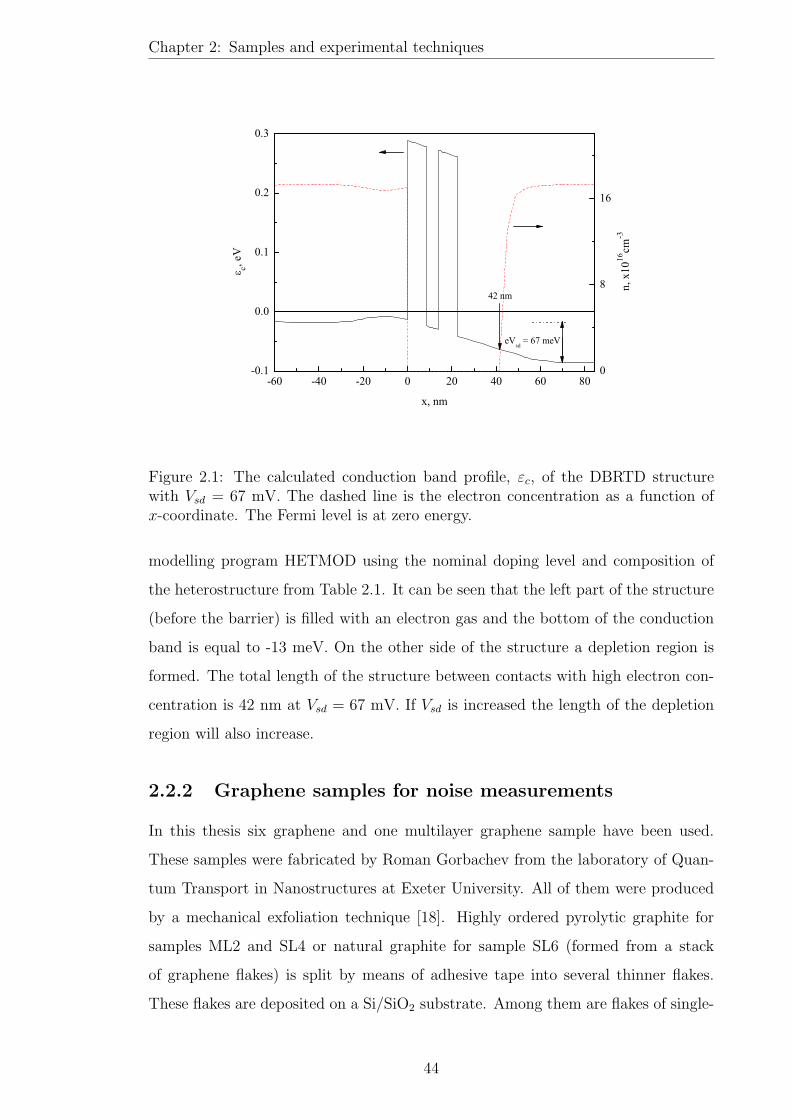
Chapter 2: Samples and experimental techniques
-60 -40 -20 0 20 40 60 80-0.1
0.0
0.1
0.2
0.3
0
8
16
42 nm
c, eV
x, nm
eVsd
= 67 meV
n, x
1016
cm-3
Figure 2.1: The calculated conduction band profile, εc, of the DBRTD structurewith Vsd = 67 mV. The dashed line is the electron concentration as a function ofx-coordinate. The Fermi level is at zero energy.
modelling program HETMOD using the nominal doping level and composition of
the heterostructure from Table 2.1. It can be seen that the left part of the structure
(before the barrier) is filled with an electron gas and the bottom of the conduction
band is equal to -13 meV. On the other side of the structure a depletion region is
formed. The total length of the structure between contacts with high electron con-
centration is 42 nm at Vsd = 67 mV. If Vsd is increased the length of the depletion
region will also increase.
2.2.2 Graphene samples for noise measurements
In this thesis six graphene and one multilayer graphene sample have been used.
These samples were fabricated by Roman Gorbachev from the laboratory of Quan-
tum Transport in Nanostructures at Exeter University. All of them were produced
by a mechanical exfoliation technique [18]. Highly ordered pyrolytic graphite for
samples ML2 and SL4 or natural graphite for sample SL6 (formed from a stack
of graphene flakes) is split by means of adhesive tape into several thinner flakes.
These flakes are deposited on a Si/SiO2 substrate. Among them are flakes of single-
44

Chapter 2: Samples and experimental techniques
ML2 SL4 SL6Length, µm 4.29 3.5 22.5Width, µm 0.6 1.5 1.5ρD, kOhm 1.4 1.7 3.5VD, V 0 V or 15 V 0 3.3 V
Table 2.2: Characteristic of graphene samples for noise measurements.
atom thickness which can be identified optically. (The interference of light from
the 300 nm SiO2 layer creates a contrast difference between single-layer and multi-
layer flakes.) As soon as the flakes are found, standard electron beam lithography
is used to define electric contacts to the flake (the contact material is Cr/Au). The
technology is more elaborate for the samples with top-gates and will be explained
below.
Three samples for noise measurements have been studied. The two samples,
SL4 and SL6, are single-layer graphene. This was proved by means of quantum Hall
effect measurements. Sample SL6 has length 22.5 µm and the highest mobility away
from the Dirac point (∼ 20000 cm2V−1s−1). The third sample, ML2, is multilayer
graphene of more than 2 layers thickness (established using optical contrast). The
geometrical sizes (the samples have approximately rectangular shape) are presented
in Table 2.2. In this table the resistivity in the Dirac point, ρD, and the position of
the Dirac point in the gate voltage are shown.
The two single-layer samples for noise measurements have the width which is
larger than 1 µm and therefore have practically zero bandgap. If the width of the
flake is small, then the edges make a significant contribution to the band structure,
forming a band gap of size increasing approximately linearly as a function of inverse
width [19]. Such narrow graphene stripes are called nanoribbons. It was shown that
the band gap of 20 nm width graphene nanoribbon is approximately 26 meV [20].
Thus if we take a stripe with 1.5 µm width, the band gap will be 75 times smaller
than 26 meV (∼ 0.35 meV corresponds to 4 K).
Fig. 2.2(a) shows a SEM image of sample SL4. The electrical contacts are shown
as outlines in the figure. Fig. 2.2(b) shows the resistivity of the sample as a function
of gate voltage at T = 0.25 K, where the characteristic peak in the Dirac point (0
V) can be clearly seen. In the inset one can see the first quantum Hall plateau
in Gxy(ν), which is observed at 2e2/h in agreement with experiment [21, 22] and
45

Chapter 2: Samples and experimental techniques
theory [23] for single layer graphene.
Sample SL6 has six terminals with the distance between two Hall contacts of
about 0.5 µm, and the area of the sample under the potential contact is about
∼ 0.5 × 0.5 µm2. The distance from the potential contacts to the nearest current
contact is about 1 µm.
46

Chapter 2: Samples and experimental techniques
Figure 2.2: (a) SEM image of sample SL4, where the positions of the contacts areshown as outlines. The inset shows a diagram of a graphene sample on n+Si substrate(purple), covered by 300 nm SiO2 (blue) and contacted by Au/Cr (yellow). Controlof the carrier density, n, is achieved by varying Vg. (b) Resistivity of the sample asa function of Vg at T = 0.25 K. The mobility is 10000 cm2V−1s−1 outside the Diracregion. The inset shows the first quantum Hall plateau in the conductance, wherethe filling factor ν = nh/4eB. Adapted from [24].
Figure 2.3: (a) Three stages of the air-bridge fabrication: electron beam lithographywith two exposure doses, development, and deposition of the metal film. (b) A false-colour SEM image of a graphene flake with a metal air-bridge gate (image is tiltedby 45).
47

Chapter 2: Samples and experimental techniques
S1 S2 S3 S5Width, µm 0.3-0.15 0.6 0.15 0.35Length, µm 5 4.3 1.45 5ρD, kOhm 6.9 4.87 6.36 14VD, V 0.05 1.11 1.68 -0.75
Table 2.3: Characteristic of graphene p-n-p samples.
2.2.3 Graphene p-n-p samples
To fabricate the p-n-p structures, we have chosen graphene flakes of rectangular
geometry on SiO2/Si substrates with a 300 nm oxide layer. The samples have the
following dimensions, in µm: L=5, W=0.24 (sample S1); L=4.3, W=0.6 (sample
S2) and L=1.45, W=0.15 (sample S3). The mobility of these samples away from the
Dirac point (at a carrier density of 3× 1011 cm−2) is 13, 11 and 6 × 103 cm2V−1s−1,
respectively. The procedure of the top-gate fabrication is illustrated in Fig. 2.3(a).
Two layers of PMMA with different molar masses are spun on the flake: a soft resist
(495K) on top of a hard resist (950K). They were then patterned using low-energy 10
keV, e-beam lithography (to achieve larger undercut in the top PMMA layer). Two
different exposure doses were used in the areas of the span and pillars of the bridge,
while the area outside the bridge was not exposed. The dose in the span is just
enough to expose the soft resist, but too small to affect the underlying hard layer.
Both layers are exposed at a larger dose in the areas of the pillars (and contacts).
The structures are then developed and covered with 5/250 nm of Cr/Au. The ‘lift
off’ removes PMMA leaving the bridge with a span up to 2 µm supported by two
pillars. Figure 2.3(b) shows an SEM image of sample S2 with a suspended top-gate
and two Ohmic contacts. The carrier mean free path in our samples l ≈ 45−100 nm
and the distance between the top-gate and the flakes is 130–210 nm. In the attempt
to produce a p-n-p structure with ballistic properties, the top-gate is made short,
100–170 nm, in the direction of the current flow.
The parameters of four samples used in the thesis are presented in Table 2.3. All
the samples are too narrow (less than 0.6 µm) to make a multiple-terminals, thus
only two-terminal samples are made and the quantum Hall effect to characterise the
sample was measured using a two-terminal geometry.
48

Chapter 2: Samples and experimental techniques
2.3 Circuitry and methods
2.3.1 I-V characteristics
A resonant current through single impurities in a DBRTD can be very small (down
to ∼ 10 pA). Thus to measure small signals a low-noise preamplifier was used and
all circuit elements were placed inside a screen room to minimise ambient noise.
An EG&G 181 current preamplifier was used to detect DC and AC currents of the
order of a few pA. The circuit we have used to measure simultaneously the current,
I(Vsd), and differential conductance, dI(Vsd)/dVsd, of the DBRTD is shown in Fig.
2.4. There are two sources of voltage: AC of 0.1 mV at 17 Hz (oscillator output
of EG & G Lock-in amplifier model 5110) and DC (DAC of a CIL Microsystem
PCI 6380). The DC signal was filtered using a low-pass RC-filter with cut-off
frequency fcut = 4 Hz. The output signal of the current preamplifier contained both
DC and AC components. The DC component was filtered with a low-pass filter
(fcut = 1 Hz) and passed to an ADC input of the PCI 6380. The AC component was
measured by the Lock-in amplifier with a time constant of∼ 1 s. The experiment was
automatiated using the software CryoMeas written for Acorn computer by Dr. C. J.
B. Ford from the Cavendish Laboratory, University of Cambridge. Instruments were
connected through IEEE-bus, except the Lock-in amplifier, because of interference
which comes from the IEEE bus. The output DC signal of the Lock-in amplifier
proportional to the AC input of the Lock-in amplifier was measured by PCI 6380.
2.3.2 Resistance measurements
Graphene structures were measured using a constant current circuit with a 100 MΩ
ballast resistor shown in Fig. 2.5. This current was ∼ 1 − 10 nA. The voltage
along the sample was measured using a low-noise voltage LI-75A amplifier of a NF
Corporation. DC voltages applied to the gates were filtered with RC-filters with
fcut = 1 Hz.
49

Chapter 2: Samples and experimental techniques
Figure 2.4: The circuit used for measurements of I(Vsd) and dI/dVsd.
Figure 2.5: The circuit used for measurements of G(Vbg) and G(Vtg).
Figure 2.6: The circuit used for measurements of voltage noise.
50

Chapter 2: Samples and experimental techniques
2.3.3 Noise
The circuit for noise measurements is shown in Fig. 2.6. A constant current regime
was used for both resistance and noise measurements (AC signal from the Lock-in
was set to zero during noise measurements). Resistance was measured before and
after noise measurements. Two low-noise voltage amplifiers were used simultane-
ously, connected to the opposite pairs of potential contacts. The output voltage
signals of these two amplifiers were paired by a cross-correlation technique using
double-channel spectrum analyser SRS785 (Stanford Research).
The cross-correlation method is used to remove the voltage noise of preampli-
fiers. By detecting only the correlated signals in both channels the analyser also
suppresses the uncorrelated noise which comes from the thermal noise of the wires
connected to the potential contacts. This technique does not suppress the current
noise of the preamplifiers. However, if the sample has the same resistance at differ-
ent source-drain voltages, the current noise (which depends only on this resistance)
gives the same contribution to the noise spectrum at any Vsd. The background
noise will therefore contain the thermal noise of the sample and some contribution
from the current noise of the preamplifiers. In the analysis presented in this thesis
the background noise is subtracted from the noise measured at a finite Vsd applied,
which leaves only non-equilibrium voltage noise of the sample.
2.3.4 Temperature and magnetic field control
For the low temperature work the current-voltage and conductance-voltage mea-
surements were carried out in a liquid Helium-4 dewar and using Helium-3 system
HelioxTL Oxford Instruments. The Helium-3 system, Fig. 2.7, allows one to mea-
sure the temperature dependence of the current in a wide range of temperatures
from 0.26 to ∼ 200 K. A superconducting magnet can generate fields up to 12 T in
the sample space.
The sample is mounted on a probe which is lowered down to the sample space.
In order to reach base temperature, 3He is released from the sorption pump and
condensed into the bottom of the sample space (the “3He pot”) by cooling it by the
1K pot. (The 1K pot contains a small volume of liquid Helium-4 and is cooled by
pumping the vapour from its surface.) When the sample is placed into the liquid
51

Chapter 2: Samples and experimental techniques
3He, the sorption pump is cooled down to the temperature of the 1K pot and it
starts pumping the 3He vapour. This pumping cools the liquid Helium-3 down to
0.26 K. (This temperature is stable for about 100 hours.) In order to change the
temperature, a heater is used to heat the sorb and the 3He pot to achieve a stable
temperature from 0.26 K to 3.2 K when the liquid 3He is evaporated. Above this
temperature the sample is in a gaseous rather than liquid surroundings. The heating
power can be controlled to reach temperatures up to 200 K.
52

Chapter 2: Samples and experimental techniques
Superconductingmagnet
3He pot
Sample
1K pot(helium-4)
Sorbtionpump(helium-3)
Probe
Mainbath(helium-4)
OVC
IVC
Figure 2.7: Scheme of Helium-3 cryostat.
53

Chapter 3
Transport through impurities in a
vertical double-barrier resonant
tunnelling diode
3.1 Introduction
In this chapter we describe transport measurements in a double-barrier resonant
tunnelling diode (DBRTD). We have observed resonant tunnelling through single-
impurity states and through double-impurity states. The effect of magnetic field on
resonant tunnelling through double-impurity states is studied.
The first part of this chapter is an introduction to the physics of resonant tun-
nelling in a DBRTD. The theoretical models used previously for analysis of resonant
currents are introduced. Some experimental results on resonant tunnelling via a sin-
gle impurity or localised states in quantum dots (QD) embedded into DBRTDs are
discussed.
In the second part, the experimental results on transport at low temperatures and
high magnetic fields are discussed in detail using a new theoretical model. Random
telegraph noise (RTN) has been observed in transport through DBRTD at 4.2 K
and analysed.
54

Chapter 3: Transport through impurities in a vertical double-barrier resonanttunnelling diode
3.2 Theory of resonant tunnelling
3.2.1 Resonant tunnelling via a quantum well in a DBRTD
One of the most studied devices in semiconductor physics is the resonant tunnelling
diode. The current-voltage characteristics of the resonant tunnelling diode have been
investigated widely in the last three decades. All possibilities of tunnelling paths
and experimental conditions (such as temperature and external magnetic field) were
investigated both experimentally and theoretically [25].
The region between the barriers, Fig. 1.4, of a DBRTD contains several subbands
due to quantum well confinement. These diodes conduct at some applied source-
drain bias, Vsd, when the bottom of the first subband aligns with the Fermi level
in the source, Fig. 1.4(a). This bias is called the threshold voltage. If larger Vsd
is applied, the Fermi level crosses the second subband and the current increases
further.
The general behaviour of the I-V characteristic of DBRTD with negative differ-
ential resistance (NDR), Fig. 1.4(e), was discussed in [26]. Lets consider a DBRTD
with one subband only, Fig. 3.1. The tunnelling current between the 3D regions via
a 2D quantum well disappears at large applied Vsd when the bottom of the conduc-
tion band in the source aligns with the bottom of this subband. The resulting shape
of the current peak is triangular, with a gradual growth at smaller bias voltages and
a rapid decrease at larger Vsd, Fig. 1.4(e). This simple model explains the presence
of NDR, see Sec. 1.2.7. If only energy subbands are considered to contribute to the
current through the DBRTD, its value below the threshold voltage should be very
small, but more detailed measurements [27] have revealed the existence of current
peaks below this voltage. These current peaks are associated with resonant tun-
nelling through zero-dimensional bound states formed by shallow donor impurities
in the quantum well.
3.2.2 Tunnelling through one impurity
The presence of impurities with energies below the first subband in a DBRTD dra-
matically increases the transparency of the structure due to resonant tunnelling
(RT) which occurs when the energy of the tunnelling electrons coincides with the
55

Chapter 3: Transport through impurities in a vertical double-barrier resonanttunnelling diode
Figure 3.1: Tunnelling through a resonant state with energy Es in a double-barrierstructure. ΓL and ΓR are the tunnelling rates from the source to the resonant stateand from the drain to the state, respectively. I2 is the total current.
impurity level, Fig. 3.1. RT through a single impurity in a barrier has been studied
in different structures, both in lateral transistors and vertical diodes [27–31]. In [27]
a vertical DBRTD based on GaAs/Al0.4Ga0.6As was investigated. The lateral size of
the structure was changed electrostatically by a lateral gate (effective cross-section
area reduced from 0.7 to 0.1 µm2). In this confined structure the authors observed
a tunnelling via single-impurity state by measuring current dependence on source-
drain voltage and side gate voltage.
In the case of resonant tunnelling from a 3D source to a 3D drain via a 0D state
in the barrier one can see a peak in I-V characteristic [32]. Due to the conservation
of energy in tunnelling, the shape of the peaks has to be triangular. A resonant
current appears when the energy Es lies between the Fermi level and conduction
band edge in the source, i. e. 0 < εs < εF . Because the density of states decreases
towards zero energy in 3D, the maximum current occurs when the impurity energy is
equal to the Fermi energy in the source contact. By applying bias one can effectively
move the impurity energy level εs from εF to zero energy (defined as the bottom of
conduction band in the source) where current is zero. At intermediate biases the
current decreases linearly with source-drain bias.
If tunnelling via a 0D impurity occurs from a 2D source, a triangular shape of
the current peak is observed with a rapid increase of the current when the impurity
energy level crosses the Fermi level in the 2DEG [33]. The current slowly decreases
if larger bias voltages are applied.
We now consider sequential tunnelling through a single resonant level as shown
in Fig. 3.1, when electron loose their phase after tunnelling from the source to the
state. An electron tunnels from the source through the resonant state with energy
Es inside DBRTD with the rate ΓL/h. This state can exist due to unintentional
56

Chapter 3: Transport through impurities in a vertical double-barrier resonanttunnelling diode
doping or can be a quantum dot formed during growth of the structure, Section
1.2.4. Then the electron tunnels to the drain with the rate ΓR/h. We can write a
system of rate equations for the currents
I1 = 2eΓL
h[fs(1− f)− f(1− fs)], (3.1)
I2 = −2eΓR
h[fd(1− f)− f(1− fd)],
where fs and fd are the Fermi-Dirac distribution functions in the source and drain,
respectively, f is the probability that the resonant level is occupied and the factor of
two accounts for the two spins. For current conservation we must have I1 − I2 = 0.
Hence we have expression for the sequential current
I1 =2e
h
ΓRΓL
ΓR + ΓL
, (3.2)
where we assumed that T = 0 and there is a finite bias. This equation shows that
to get the largest current we have to have ΓL = ΓR, which corresponds to an equal
distance from the impurity to the drain and to the source. Therefore, impurities
placed in the middle of the structure can be more easy detected. If this impurity is
placed near one of the contacts then the tunnelling rate between them will be large
but the current through the structure will be determined by the smaller tunnelling
rate.
3.2.3 Tunnelling through two states
The theory of RT via two impurities was proposed in [34] and this effect was observed
experimentally on a short lateral transistor [35]. It is difficult to distinguish between
one- and two-impurity RT in the ohmic regime of conduction – at zero bias both
effects give peaks in the conductance as a function of impurity energy. However,
their I-V characteristics are quite different. Single-impurity RT produces a step-like
I-V characteristic, with the threshold of the current corresponding to the impurity
level coinciding with the Fermi level in the contact [32]. In comparison, the I-V
characteristic of two-impurity RT has a distinct peak at the voltage, corresponding
to the alignment of the two impurity levels [35] below the Fermi level in the source.
In [36] an impurity state in a RTD was used to detect the electronic structure of
57

Chapter 3: Transport through impurities in a vertical double-barrier resonanttunnelling diode
Figure 3.2: a) Conduction-band profile of a device used to probe the states of a QDwith an impurity state in a DBRTD. The inset shows a schematic overview of thestructure, indicating the depleted region around the tungsten wires. The quantumdot is formed between the two DBRTDs. b) I-V characteristics measured at B = 0 Tand Vg = −50 mV for different temperatures. The solid line is for 0.3 K, the dotted4.2 K, and the dashed 10 K. For Vc < 0.12 V the current is less than 0.1 pA and hasno fine structure. Note the emitter corresponds to source and the collector to drainin my text. Adapted from [36].
an electrostatically defined quantum dot, Fig. 3.2a. The impurity state localised in
the DBRTD moved in energy with applied voltage and at several values of Vsd sharp
resonances occurred. These resonances are only possible when the energy level of
the impurity aligns with an energy level in the QD. If we denote the energy state of
the impurity by εi and the energy state in the QD by εdot then the corresponding
shift of the states with Vsd are given by linear relations:
εi = ε0i − eVsdηi, (3.3)
εdot = ε0dot − eVsdηdot,
where ε0i and ε0
dot are the energy states of the impurity and QD, respectively, at
Vsd = 0, and ηi and ηdot are the leverage factors (coefficients of proportionality
between energy and Vsd which are dependent on the position of the impurity and
dot along the RTD). The values of ηi and ηdot can change from 0 (state placed near
the source) to 1 (placed near the drain). The position of the resonance can be found
from the equality Ei = Edot, where the energies are taken from Eq. 3.4. The voltage
where the resonance occurs is
V rsd =
ε0dot − ε0
i
e(ηdot − ηi). (3.4)
The results of measurements with several peaks in the I-V characteristic for
58

Chapter 3: Transport through impurities in a vertical double-barrier resonanttunnelling diode
different temperatures are presented in Fig. 3.2(b). It is seen that current peaks
occur, with a finite background due to the overlap of the tails of the nearest peaks.
In [37] tunnelling via two QDs formed by GaAs quantum wells between AlAs
barriers (triple barrier structure) in series was studied. The barrier between the two
QDs was small in comparison to the barriers between the QDs and the contacts.
This helped to form a strong coupling between two electron states in QDs to form
a new molecular state. The authors observed steps, but not peaks, in the I-V
characteristic which they attribute to the tunnelling via a state in the quantum-dot
molecule. The current through this molecular state was described by the Eq. 3.2
for a single state in the well.
3.2.4 Effect of magnetic field
Impurity energy levels are affected by an external magnetic field, B, when the spread-
ing of the wavefunction of the state becomes comparable to the magnetic length,
lB =√
h/eB. Magnetic field acts as an additional confining potential on the elec-
tron wavefunction and hence causes a (diamagnetic) shift of the energy level. It has
been shown in [38], Fig. 3.3(a), that for a parabolic potential in the XY -plane
V (x, y) =1
2m∗ω2
0(x2 + y2), (3.5)
the energy spectrum in magnetic field oriented in the z-direction (direction of the
current) is given by
εN,l = (2N + |s|+ 1)h
√ω2
0 +ω2
c
4− s
2hωc, (3.6)
where m∗ is the effective mass of electrons, ω0 determines the curvature of the poten-
tial, N is the radial quantum number (N = 0, 1, 2, ...,), s is the angular momentum
quantum number (s = 0,±1,±2, ...,), and ωc = eB/m∗ is the cyclotron frequency.
The potentials of a shallow impurity and QD can be (in the first approximation)
taken as parabolic potential with an effective parameter ω0. The influence of mag-
netic field on the ground state, ε0,0, is the smallest. If ωc À ω0 then we have a
linear dependence of energy on B-field, as for a zero Landau level, ε0,0 = hωc/2.
In the opposite case, ω0 À ωc, a deep level (or weak magnetic field) will not be
59

Chapter 3: Transport through impurities in a vertical double-barrier resonanttunnelling diode
0 3 6 9 12 1515
16
17
18
19
0 2 4 6 80
10
20
30
F, meV
B, T
3D GaAsn = 2 · 1017 cm-3
g = - 0.44
GaAs
0 = 5 meV
0,-2
0,3
0,2
0,-1
0,1
0,0
N,l, m
eV
B, T
Figure 3.3: (a) Several energy levels of the impurity with hω0 = 5 meV as a functionof magnetic field, Eq. 3.6. (b) Oscillations of the Fermi level in magnetic field, Eq.3.7.
weakly affected by the magnetic field and we can expand the ground state energy as
ε0,0 ≈ hω0(1+ω2c/8ω
20), which is quadratic in B. If we consider an anisotropy in the
potential, for example, the well has a different size in x and y direction, then the
magnetic field effect on the energy state will be more complicated than that given
by Eq. 3.6.
The Fermi level in the source shifts as a function of magnetic field. The movement
of the Fermi level at fixed concentration, n, of the 3D electron gas in the source can
be determined from [2]
n =
√2(m∗)3/2
π2h3 µBB∑N, σ
√EF − (2N + 1)µBB + σgµBB (3.7)
where µB = eh/2m∗ is the effective Bohr magneton, spin number σ takes values
±1/2, and g is the Lande g-factor of electrons. At a fixed concentration the Fermi
level oscillates as a function of magnetic field, Fig. 3.3(b). In high magnetic fields
spin splitting has to be taken into account (the last term in Eq. 3.7).
From an experimental point of view, a parabolic potential is a good approxima-
tion of the confinement potential of a QD. Many authors [33,36,37,39] used Eq. 3.6
to explain the shifts of the peaks or steps in the tunnelling current as a function of
60

Chapter 3: Transport through impurities in a vertical double-barrier resonanttunnelling diode
n-GaAs
eVsd
B
n-GaAs
AlG
aA
s
AlG
aA
s
GaAs
B
X
Y
ZmL
mR
En
erg
y
Impurities
Z
Figure 3.4: Schematic presentation of the double-barrier resonant tunnellingGaAs/Al0.33Ga0.67As structure with an applied bias. The two dots indicate im-purities in resonance.
Vsd and magnetic field.
Because tunnelling is sensitive to the local density of electron states in the source,
the local structure of the Landau levels in GaAs has been studied by a tunnelling
with magnetic field applied [40], where a single impurity of radius 10 nm (esti-
mated from the expression r ∼√
2h/m∗ω0) was used as a detector. In magnetic
field parallel to the current the local density of states can be detected, because the
maximum current occurs in the region of the impurity and using magnetic field the
effective impurity size can be changed (in strong magnetic field this size is given by
r ∼√
2h/m∗ωc). The authors have also observed a diamagnetic shift of the ground
state (N=0, s=0) described by Eq. 3.6.
In [39] resonant tunnelling from a 2DEG via InAs QDs embedded in an AlGaAs
barrier was studied. Two orientations of magnetic field with respect to the current
were used to estimate the size of the resonant state. When magnetic field perpen-
dicular to the current was applied, the variation in the voltage corresponding to the
current peak is determined by
e∆V = −βe2B2
2
(〈z2e〉
m∗ − γ〈z2
d〉md
), (3.8)
where√〈z2
e〉 is the spatial extent of the electron wave function in the emitter,
estimated using self-consistent numerical calculations,√〈z2
d〉 is the spatial extent
of the barrier state, m∗ and md are the electron masses for the electron and the
electron in the well, β is the leverage factor, and γ is a geometric factor related to
the shape of the confinement potential.
61

Chapter 3: Transport through impurities in a vertical double-barrier resonanttunnelling diode
3.3 Experiment and analysis
3.3.1 General I-V characteristic of DBRTD
Our experiments have been performed on a vertical GaAs/AlGaAs diode structure
(KIIORe23b, supplied by Giancarlo Faini from the Laboratoire de Photonique et
Nanostructures, CNRS in Marcoussis, France) at temperatures down to T = 0.25 K.
Two AlGaAs barriers of width 8.7 nm confine a 5 nm wide GaAs quantum well.
The GaAs contacts contain doped regions which are separated from the barriers
by spacers of 20 nm and 30 nm thickness. Fig. 3.4 shows the band diagram of
the structure with a positive bias applied to the right contact. In the lateral (XY)
direction the sample is etched into a pillar with a diameter of 70 nm [41]. The small
cross-sectional area of the device allows one to detect the presence of individual
impurities in the current through the structure [42].
We have studied sample KIIORe23b in a helium dewar at 4.2 K by measure-
ments of I-V characteristics at different ranges of Vsd. Measurements of the signals
below 100 nA were performed using a low-noise current preamplifier EG & G 181
(which can detect DC currents as small as 0.25 pA. A general picture of the I-V
characteristic of this sample is shown in Fig. 3.5. The I-V characteristic has a
diode-like behaviour with threshold voltages at 0.17 V and -0.15 V. Negative dif-
ferential conductance (NDC) has been observed in the regions around ±0.1 V. The
experiments below concentrate on the region below the threshold voltage, to study
the resonances that cause this NDC.
3.3.2 Random telegraph noise in DBRTD at 4.2 K
The I-V characteristic measurements below 0.1 V have shown several current peaks
which are due to tunnelling through localised states inside the DBRTD. Around
these peaks the current is observed to switch between two states with an approximate
period of 1 s. This RTN at 4.2 K is shown in Fig. 3.6. On the graph increasing and
decreasing sweeps of the bias voltage are shown. It appears that the direction of
the sweep has no effect on the RTN, that is there is no hysteresis effect. The most
intense noise occurs in the range from 60 mV to 80 mV in Vsd around the current
peak of 20 pA. It can be seen that there are two main states for the current indicating
62

Chapter 3: Transport through impurities in a vertical double-barrier resonanttunnelling diode
-0.1 0.0 0.1 0.2-12
-8
-4
0
4
8
-0.1
0.0
0.1
0.2
0.3
0.4
0.5
0.6
Vsd
, V
I, nA
KIIORe23bT = 4.2 K
G,
S
Figure 3.5: The I-V characteristic (solid line) of the KIIORe23b sample from -0.15V to 0.17 V at 4.2 K. The dotted line shows the simultaneously measured differentialconductance, G, as a function of Vsd. Negative differential conductance near ±0.1V corresponds to the presence of peaks in the I-V characteristic.
that noise originates from the switching of a single impurity (however, there are also
small-amplitude switchings with much lower rate). The two states look identical
when shifted along Vg. RTN can be produced by charging and discharging of an
impurity in one of the contacts or in the barrier close to the drain. In this case
charging this impurity does not change the amplitude of the peak, but it creates
an effective source-drain bias, which shifts the peak position by a constant voltage.
In the insert of Fig. 3.6 a slow voltage sweep is shown. The peak at 70.7 mV is
shifted by the change in occupancy of the impurity state to a new position 73 mV.
This fluctuating peak has good reproducibility with time and from one cool-down
to another (the amplitude varies between 19 and 22 pA).
To analyse this RTN we have divided the Vsd region from 56 mV to 78 mV
around the peak (with 27500 data points) into 50 smaller regions (with 550 point in
each). Then we have calculated the distribution of the current in each region. The
resulting histogram was fitted by a double Gaussian function to find the maxima of
the distribution. The results of the analysis are shown in Fig. 3.7(a,b). The solid
circles represent the first state which is populated at smaller Vsd, and the empty
circles are related to the second state, which is populated at the larger biases. The
63

Chapter 3: Transport through impurities in a vertical double-barrier resonanttunnelling diode
0 20 40 60 80 100
0
10
20
30
40
50
60
60 65 70 75 800
4
8
12
16
20
Sweep rate = 600 mV · h-1
KIIORe23bT = 4.2 K
I, pA
Vsd
, mV
Sweep rate = 4 mV · h-1 I,
pA
Vsd, mV
2.24 mV
Figure 3.6: The I(Vsd) characteristic of sample KIIORe23b at 4.2 K measured twicewith sweep rate 600 mVh−1. One can see switching between two states. Inset: theI(Vsd) characteristic measured with sweep rate 4 mVh−1 with results presented asindividual points. The shift in Vsd between the two states is about 2.4 mV.
position of the minimum between the two peaks in the histogram can be used to
distinguish the two states from each other. The total number of counts from this
minimum to the left represents the total time of population of the low-current state.
We can find the probability to find an electron in state 2 as a function of Vsd by
dividing this number by the total number of counts, Fig. 3.7(c), which shows an
approximately a linear dependence on Vsd.
It is expected that RTN rate has an exponential increase with increasing tem-
perature [6] because it is easier to occupy an impurity at higher temperature. Thus
to get a more stable system without RTN lower temperatures are required.
3.3.3 I-V characteristics at T=0.25 K
Fig. 3.8 shows an I-V characteristic of sample KIIORe23b at 0.25 K measured in
a Helium-3 cryostat. The threshold voltage has not changed in comparison to that
observed in a dewar at 4.2 K, Fig. 3.5. One can distinguish several regions in the
I-V characteristic: a region with small peaks of amplitude less than 0.1 nA and
64

Chapter 3: Transport through impurities in a vertical double-barrier resonanttunnelling diode
Figure 3.7: (a) Current as a function of Vsd of sample KIIORe23b for two separatedstates at 4.2 K. State 1 is shown by filled circles and state 2 by empty circles. (b)Distribution of the currents at Vsd = 64.122 mV (shown in (a) by dashed verticalline). Arrow shows current value (5.45 pA) taken to separate two states. Solid lineshows fit using sum of two Gaussian functions. (c) Probability to find an electronin state 2 as a function of Vsd. The solid line is a linear fit.
small background; a region with larger peaks with amplitudes of about 0.1 nA on
a background of about 0.1 nA; and a larger Vsd region where the current increases
rapidly at the threshold voltage of 0.15 V. We are interested in the first region with
small well resolved peaks of 10 pA amplitude.
We have focused our attention to the range of voltages from 55 mV to 70 mV,
where several peaks are seen. This region of the source-drain bias (with the current
of the order of 10 pA) below the threshold voltage corresponds to transport via
impurities in the structure. At the beginning of the experiment, the I-V charac-
teristic was not stable and many RTN signals which not only shifted the current
peaks but also changed their amplitudes were observed. The structure of the peaks
was stabilised by sweeping the voltage in this range of Vsd for two weeks at base
temperature. Fig. 3.9(a) shows the I-V characteristic of sample KIIORe23b where
65
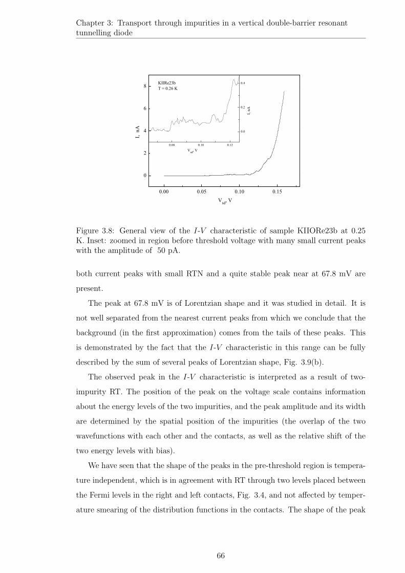
Chapter 3: Transport through impurities in a vertical double-barrier resonanttunnelling diode
0.00 0.05 0.10 0.15
0
2
4
6
8
0.08 0.10 0.12
0.0
0.2
0.4
KIIRe23bT = 0.26 K
I, n
A
Vsd, V
I, n
A
Vsd, V
Figure 3.8: General view of the I-V characteristic of sample KIIORe23b at 0.25K. Inset: zoomed in region before threshold voltage with many small current peakswith the amplitude of 50 pA.
both current peaks with small RTN and a quite stable peak near at 67.8 mV are
present.
The peak at 67.8 mV is of Lorentzian shape and it was studied in detail. It is
not well separated from the nearest current peaks from which we conclude that the
background (in the first approximation) comes from the tails of these peaks. This
is demonstrated by the fact that the I-V characteristic in this range can be fully
described by the sum of several peaks of Lorentzian shape, Fig. 3.9(b).
The observed peak in the I-V characteristic is interpreted as a result of two-
impurity RT. The position of the peak on the voltage scale contains information
about the energy levels of the two impurities, and the peak amplitude and its width
are determined by the spatial position of the impurities (the overlap of the two
wavefunctions with each other and the contacts, as well as the relative shift of the
two energy levels with bias).
We have seen that the shape of the peaks in the pre-threshold region is tempera-
ture independent, which is in agreement with RT through two levels placed between
the Fermi levels in the right and left contacts, Fig. 3.4, and not affected by temper-
ature smearing of the distribution functions in the contacts. The shape of the peak
66

Chapter 3: Transport through impurities in a vertical double-barrier resonanttunnelling diode
55 60 65 70
5
10
15
60 64 680
5
10
15
b
I, p
A
Vsd, mV
KIIRe23bT = 0.26 K
a I-Vsd Fit Lorentz peaks
I, p
A
Vsd, mV
Figure 3.9: The I-V characteristic of sample KIIORe23b at 0.25 K from 55 mV to79 mV. (a) Several sweeps with small RTN. (b) Fitting of the I-V characteristic(empty circles) using seven Lorentzian peaks (dashed curves). The resulting fit isshown by a solid thick line.
is described by a Lorentzian [35]:
I(∆Vsd) =2e
h
ΓLΓR|HLR|2(βLRe∆Vsd/2)2ΓLΓR/(ΓR + ΓL) + (ΓR + ΓL)(ΓRΓL + |HLR|2) , (3.9)
where ΓL(ΓR) is the tunnelling rate from the left (right) impurity to the left (right)
contact, HLR is the overlap integral between the wavefunctions of the two impurities,
βLR = βR − βL, βL,R = dεL,R/deVsd is the leverage factor related to the shift of the
impurity level with a voltage applied, εL and εR are the energies of two levels (with
respect to the Fermi level in the left contact), ∆Vsd is the bias voltage with respect
to the resonant value V r. The amplitude of the peak
I0 = I(∆Vsd = 0) =2e
h
ΓLΓR|HLR|2(ΓR + ΓL)(ΓRΓL + |HLR|2) , (3.10)
and the half-width at half-height is determined by
W1/2 =2
βLRe(ΓL + ΓR)
√1 +
|HLR|2(ΓL + ΓR)2
. (3.11)
67

Chapter 3: Transport through impurities in a vertical double-barrier resonanttunnelling diode
65.5 66.0 66.5 67.0 67.5 68.00
2
4
6
8
10b KIIRe23b
T = 0.26 K
Vsd, mV
B, T
-23
-18
-14
-9.2
-4.6
0
4.6
9.2
14
18
23
65.5 66.0 66.5 67.0 67.5 68.00
2
4
6
8
10
G, nS
I, pAKIIRe23bT = 0.26 K
Vsd
, V
B, T
3.2
4.7
6.3
7.8
9.4
11
12
14
16a
Figure 3.10: (a) Grey-scale of the current as a function of Vsd and B of sampleKIIORe23b at 0.25 K (first measurement). The darkest region represents the largestcurrent. The black line at B = 1.6 T is RTN. (b) Grey-scale of the conductance asa function of Vsd and B measured simultaneously with the current. NDC is seen aswhite regions on the graph.
68

Chapter 3: Transport through impurities in a vertical double-barrier resonanttunnelling diode
3.3.4 Effect of magnetic field on the current peak
To understand more about the properties of these two impurities, a magnetic field
parallel to the current has been applied. Fig. 3.10(a), shows how the I-V charac-
teristic changes as a function of magnetic field. The differential conductance, Fig.
3.10(b), shows the position of the current peak more distinctly. The reproducibility
test (Fig. 3.11) performed confirmed that there was no effects on the shift of the
peak due to RTN.
The dark line near 1.6 T in Fig. 3.10(a) is indeed the second state of a RTN in
the I-V characteristic, which has a larger current. The studied peak in the current
was stable during several days when magnetic field dependance experiments have
been performed. This is confirmed by repeated experiment, Fig. 3.11, where no
RTN at B = 1.6 T was detected (one has to notice though that the RTN seen
in Fig. 3.10 around B = 1.6 T is not associated to a special B-field, and it only
occurred in that moment of time during the long term experiment).
Fig. 3.11 shows the current characteristics for the peak at Vsd = 67 mV in
magnetic fields up to 10 T. The main feature is a shift of the peak to smaller
voltages in weak magnetic fields. From 0 T to 2 T the amplitude of the current
peak does not change, but above 2 T the amplitude decreases linearly as a function
of magnetic field and becomes zero at 4 T, Fig. 3.12. In the range of magnetic
fields from 4 T to 8 T there are two current peaks with a random switching between
them. In this region the amplitudes of the peaks can both increase or decrease with
Vsd and B. Another region begins at 8 T, when another current peak is seen, whose
amplitude increases monotonically and the position of the peak shifts to smaller
voltages, indicating a similar origin for this peak shift as for the peak observed at
small magnetic fields (below 4 T). To analyse the shift of the peak seen below 4 T
we have used a fitting procedure with a Lorentz shape function (analogous to Eq.
3.9 but with a background):
I = y0 +ALω2
4(x− xc)2 + ω2, (3.12)
where y0 is a background current which probably comes from the tails of the nearest
peaks, xc is the position of the maximum of the peak in Vsd-scale, AL is a current
amplitude, and ω is the full width at half maximum.
69

Chapter 3: Transport through impurities in a vertical double-barrier resonanttunnelling diode
65.5 66.0 66.5 67.0 67.5 68.00
2
4
6
8
10KIIRe23bT = 0.26 K
I, pA
Vsd, mV
B, T
4.0
6.3
8.6
11
13
16
Figure 3.11: Grey-scale of the current as a function of Vsd and B of sample KI-IORe23b at 0.25 K (second measurement).
Figure 3.12: Current as a function of bias at different magnetic fields. The curvesare shifted vertically from the curve at B = 0 T for clarity.
70

Chapter 3: Transport through impurities in a vertical double-barrier resonanttunnelling diode
0 1 2 3
66.8
66.9
67.0
67.1
67.2
Set 1
Set 2
KIIORe23b
T = 0.26 K
Vr sd
, m
V
B, T
Figure 3.13: The position of the current peak as a function of magnetic field from 0T to 3 T for two sets of experiments.
Figure 3.13 shows the shift of the current peak due to magnetic field. On the
graph two sets of experimental data are presented, taken a day apart. One can see
a good agreement in the shift of the current peak position as a function of magnetic
field, which can be described as a linear dependence from 0.7 T to 3 T:
V rsd[V] = 0.06734− 1.784 · 10−4B[T]. (3.13)
This (diamagnetic) shift has different sign to be explained in terms of single impurity
diamagnetic shift. Indeed, according to Eq. 3.6 in strong magnetic field one should
see a liner diamagnetic shift up with increase of the energy state ε0,0 = hωc =
heB/2m∗ and it is required a larger Vsd to achieve a new resonant level of the
impurity. For the two-impurity RT the shift of the current peak comes from the
difference of the shift of the two levels (if for example both levels are shifted with B
by exactly the same energy, no shift of the peak in I-V will be detected). On the
other hand, if the left impurity (close to the source) shifts faster in B-field than the
right impurity we will observe a shift of the current peak to lower voltages as seen
in experiment.
71

Chapter 3: Transport through impurities in a vertical double-barrier resonanttunnelling diode
Figure 3.14: Conductance as a function of electron energy and overlap integral;Γ = 0.1 meV; εr = 1 meV, Eq. 3.19.
3.3.5 Analysis of the current peak in the presence of mag-
netic field
Let us consider the situation of tunnelling through two impurities inside a resonant
tunnelling diode at zero temperature. From [34] the conductance
G =e2
hT (ε, ε1, ε2) =
e2
h
4ΓLΓR|HLR|2|(ε− ε1 + iΓL)(ε− ε2 + iΓR)− |HLR|2|2 , (3.14)
where T (ε, ε1, ε2) is the transmission probability for an electron with energy ε
through two localised states at ε1 and ε2. (The leak rates and overlap integral
can change with applied voltage, but at the low voltages we neglect these changes.)
If we assume that ε1 = ε2 = εr and ΓL = ΓR we can plot the conductance (Eq.
3.14) as a function of the electron energy ε and overlap integral, Fig. 3.14. One can
see that if HLR ¿ ΓL one gets a single peak in the conductance, which splits into
two in the case when HLR À ΓL.
The energies of the impurities as a function of bias can be written in the following
form
ε1 = ε01 − βLeV , (3.15)
ε2 = ε02 − βReV , (3.16)
where ε01 and ε0
2 are the localised state energies without bias, and V is an applied
voltage. In this vertical double-barrier structure we do not have a gate to vary the
energy levels of the impurities (which would be the case in lateral structures with
72

Chapter 3: Transport through impurities in a vertical double-barrier resonanttunnelling diode
Figure 3.15: Normalised amplitude of the current peak as a function of resonancelevel position εr and overlap integral H; Γ = 0.3 meV; µ = 4 meV, Eq. 3.19.
double quantum dots). However, we can use an external magnetic field which will
similarly shift the energy levels. If the potential energy of the localised states can
be presented by a parabolic potential, then we can rewrite expressions (3.15) and
(3.16) taking into account the diamagnetic shift of each impurity level [38]:
ε1 =
√(ε0
1)2 +
(hωc
2
)2
− β1eV, ε2 =
√(ε0
2)2 +
(hωc
2
)2
− β2eV, (3.17)
where ωc = eB/m∗ is the cyclotron frequency of an electron with effective mass m∗ =
0.067m0 in bulk GaAs. Here we assume that the leak rates do not depend on applied
magnetic field and the magnetic field orientation is parallel to the current. This
means that magnetic field does not change the size of the impurity wave function
in the direction of current flow and thus the leak rates and the overlap integral are
not changed significantly by magnetic field.
As we are interested in the amplitude of the current, we need to discuss the
situation at resonance, which happens when the energies of the two impurities are
equal. The resonant energy of the two impurities (counted from the bottom of the
conduction band in the source) is
εr =
(1 +
β1
β2 − β1
) √(ε0
1)2 +
(hωc
2
)2
− β1
β2 − β1
√(ε0
2)2 +
(hωc
2
)2
. (3.18)
This is found from the condition ε1 = ε2 using Eq. 3.17. Integration of Eq. 3.14 over
energy with infinite limits can be replaced by integration over a semi-finite interval
due to the step-function shape of the Fermi-Dirac distribution function. (The full
procedure of integration is presented in Appendix A.) The resulting expression for
73

Chapter 3: Transport through impurities in a vertical double-barrier resonanttunnelling diode
the maximum current is
Imax =e
h
ΓLΓR|HLR|2H(H2 + Γ2)
[1
2ln
((µ + H − εr)2 + Γ2
(µ−H − εr)2 + Γ2
)+
+H
Γ
[tan−1
(µ + H − εr
Γ
)+ tan−1
(µ−H − εr
Γ
)+ π
]], (3.19)
where H =√|HLR|2 − 1
4(ΓL − ΓR)2 and Γ = 1
2(ΓL + ΓR).
Fig. 3.15 shows the dependence on resonant level position εr and overlap integral
H of the current amplitude normalised over the current magnitude at εr = 0. In the
figure one can see the transition from a smooth ’single-step’ monotonic dependance
for H ¿ Γ to a ’two-step’ dependence in the case when H À Γ.
3.3.6 Diamagnetic shift and current amplitude
The fact that the amplitude of the current peak does not depend on magnetic field
(from 0 T to 2 T), Fig. 3.16, tells us that the overlap of the wave functions is not
affected by magnetic field. This means that in Eq. 3.19 HLR is not affected by B-
field, that is the impurities are spatially aligned along the direction of the magnetic
field (i.e. the distance between the impurities in the XY-plane is smaller than the
magnetic length, 18 nm at 2 T).
We interpret the shift of the peak by the diamagnetic shift of impurity levels,
caused by squeezing the electron wavefunctions in the XY-plane of the structure. If
two impurities were shifting equally in magnetic field, the position of the resonance
would remain unchanged. The shifts towards smaller Vsd means that the shift of the
left impurity is stronger than that of the right impurity (Fig. 3.4). (The fact that
the resonance is observed at a positive bias also means that the original (zero bias)
position of the left energy level is lower than that of the right level.)
The position of the current peak in voltage, V r, can be written analytically for
a simple model of two parabolic confining potentials of the two impurities (one can
show that the results of this approximation are close to that obtained for Coulomb
74

Chapter 3: Transport through impurities in a vertical double-barrier resonanttunnelling diode
0 1 2 30.0
0.4
0.8
1.2
66.4 66.8 67.2 67.60
4
8
12
b
Experiment H
LR=0.01 meV
HLR
=0.1 meV H
LR=0.3 meV
HLR
=0.5 meV
B, T
I max
(B) /
I max
(0)
a
I, p
A
Vsd, mV
B 0.7 T 3.0 T
Figure 3.16: (a) The ratio of the current amplitudes as a function of magnetic fieldfrom 0 T to 3.5 T. Four curves generated from Eq. 3.18 with different overlapparameter, HLR are presented. (b) Current as a function of bias, Vsd, for twomagnetic fields (0.7 T, 3 T), shown in (a) with arrows.
impurities [4]):
V r =1
eβLR
√(εR − ε0R)2 +
(hωcR
2
)2
−√
(εL − ε0L)2 +
(hωcL
2
)2
+ ε0R − ε0L
,
(3.20)
where εL and εR are the energies of the two levels, ε0R and ε0L are the energies
of the bottoms of the parabolic potentials, ωcR,L = eB/mR,L. The difference in
the diamagnetic shifts of the two impurities, controlled by the difference in their
cyclotron masses, can be easily obtained from the linear shift seen above 1.5 T, Fig.
3.17, given by Eq. 3.13. (The linear dependence in Eq. 3.20 corresponds to the
situation when the diamagnetic shifts are stronger than the ground state energy of
the impurities. In other words, the parabolic potential in the XY plane is weaker
than the magnetic field potential at B > 1.5 T.) This gives us directly the relation
between the two cyclotron masses (m∗ is the bulk electron mass in GaAs), with
75

Chapter 3: Transport through impurities in a vertical double-barrier resonanttunnelling diode
Figure 3.17: Position of the current peak as a function of magnetic field, with afitting curve, Eq. (3.20).
mL < mR:m∗
mR
− m∗
mL
= −0.2βLR. (3.21)
We can obtain a self-consistent picture by assuming that the two impurities are
positioned in the AlGaAs barriers, close to the interfaces with the GaAs quantum
well, Fig. 3.4. The geometry of the structure will then give the value of βLR ∼ 0.1
and therefore the difference between the two masses of about 2%. The fitting of the
whole curve in Fig. 3.17 gives then the values of the ground state energies of the
impurities in the parabolic potential: εR − ε0R ' εL − ε0L = 1.5 meV. This value
is about four times smaller than the value obtained from the comparison of the
Coulomb potential (with the bulk mass) with the parabolic potential. Positioning
of the impurities at the AlGaAs/GaAs interfaces accounts for the difference, as half
of the Coulomb potential is now replaced by a high potential wall.
Let us now discuss the origin of the decrease in the current in Fig. 3.16(a) from
B = 2 T to 4 T. One possibility is that the level of the left impurity is shifted
up with magnetic field and at B ∼ 2 T it becomes higher than the Fermi level
in the left contact, Fig. 3.4. Then the range of fields where this decrease occurs
(∼ 1 T) is related to the width of the resonance. There is a problem, however, in this
explanation because the width of the resonance determined from the current peak,
Fig. 3.16(b), appears to be two times smaller than expected for such a scenario. This
fact requires further investigation: it is possible that other effects (such as a decrease
of the overlap in magnetic field, or slowing down of the energy level shift near the
Fermi level) are responsible for the decrease of the current peak in magnetic field.
76

Chapter 3: Transport through impurities in a vertical double-barrier resonanttunnelling diode
The result of fitting using Eq. 3.18 for different overlaps (HLR) are also presented.
We can conclude that the best fit is observed for the parameter HLR < 0.1 meV,
which implies small overlap between the two resonant states.
3.4 Conclusions
Resonant tunnelling through two impurities has been observed for the first time in
a vertical double-barrier resonant tunnelling diode structure. The current-voltage
characteristic has been studied in parallel magnetic field and analysed with the help
of the developed model. It was shown that resonant tunnelling in magnetic field gives
information about the properties of the impurities: the energy levels, the effective
electron mass and spatial positions of the impurities in the structure.
77

Chapter 4
Charge carrier transport in
graphene
4.1 Introduction
The aim of this chapter is to describe the diffusion model and simplifications we
have used to model carrier transport in graphene. The model is used successfully to
predict the energy dependence of the resistance in top-gated structures in graphene
flakes with low mobility. There is a striking deviation from the model when a p-n
junction is formed in graphene flakes where the carriers have a higher mean free
path. This is discussed with the help of a ballistic transport model by Cheianov and
Fal’ko [43].
Transport through p-n and p-n-p junction has been calculated numerically both
in the diffusive and ballistic regime. For all calculations we have used Comsole
FEMLab software, which uses a similar programming language to MatLab often
used for scientific computations. (All source codes with comments are placed in
Appendixes.) The code for the ballistic model was written by F. Guinea (Instituto
de Ciencia de Materiales de Madrid, CSIC, E28049 Madrid, Spain). To describe os-
cillatory behavior observed in the transmission probability through a p-n-p junction
we have used a code also provided by F. Guinea.
78

Chapter 4: Charge carrier transport in graphene
4.2 Graphene
Graphene is a two-dimensional crystal of carbon atoms connected in a honeycomb
lattice. This single atom thick crystal was first created experimentally in 2004 by
a University of Manchester research group lead by Andre Geim [18, 44]. Graphene
has attracted considerable interest after its discovery, most notably because of its
unusual, linear dispersion relation for the charge carriers [45], which emulates high
energy relativistic physics in table-top experiments. Such phenomena as Klein tun-
nelling [46] and Zitterbewegung [47] which have analogues in quantum electrody-
namics were theoretically predicted in 2006 in graphene.
The vast majority of experiments to date have been carried out on graphene
made by a mechanical exfoliation technique [18] where a graphite monocrystal is
repeatedly split into thinner and thinner slices using an adhesive tape. These slices
may contain many layers of graphene and also single atomic layers. Then the slices
are deposited on an oxidised Si wafer. As soon as graphene has been deposited, the
problem of finding a monolayer in the deposit arises. It was found experimentally
that the graphene layer affects the resonant backscattering of light through the
SiO2 on the Si surface, and the visibility of single/few layer graphene problem has
been solved by means of thin-film optics theory [48, 49], where the dependence of
reflected light intensity from the structure on angle of light beam incidence, thickness
of substrate, and dielectric constant of the substrate has been calculated. It was
discovered that single-layer graphene is better seen on top of Si wafer with specific
thickness (100 nm and 300 nm) of SiO2.
In spite of a single-atom thickness, graphene is chemically stable [18] and able
to withstand lithography processing. In order to verify the single atomic nature of
graphene, quantum Hall effect [21,22] and Raman spectroscopy [50] are used. High
quality samples with a six-terminal Hall bar geometry have revealed, in quantising
magnetic fields, a peculiar half-integer quantum Hall effect in monolayer graphene
[21, 22]. In Raman spectra so-called D peak can help to distinguish a single-layer
from bilayer and triple layer graphene [50].
In the following subsections an introduction to the physics of graphene based on
a low energy approximation of transport on honeycomb lattice is presented.
79

Chapter 4: Charge carrier transport in graphene
Figure 4.1: Graphene honeycomb crystal lattice. Two independent sublattices Aand B are shown by different colours.
4.2.1 Crystal lattice
All the unique properties of graphene emerge from its honeycomb crystal lattice
structure. The lattice of graphene consists of hexagons with carbon atoms placed
in their corners with angles of 120 between them. The distance between nearest
neighbours is d = 0.142 nm. In a unit cell of graphene, as shown in Fig. 4.1, there
are two atoms shown by different colours. All atoms of type A, shown in blue, form
a triangular sublattice where the atoms’ positions can be expressed in terms of unit
lattice vectors a1 and a2:
rA = ma1 + na2, (4.1)
where m and n take values 0,±1,±2.... The unit vectors in two-dimensional space
for the lattice shown in coordinate system (X, Y ) in Fig. 4.1 are
a1 =d
2
(3,√
3)
, a2 =d
2
(3,−
√3)
. (4.2)
The second sublattice made from B-type atoms is shifted by a vector δ3. A sublat-
tice, ΛA, has a set of all possible vectors rA and B sublattice, ΛB, contains vectors
rA − δ3. The vectors defining the nearest neighbours in sublattice B, shown by the
80
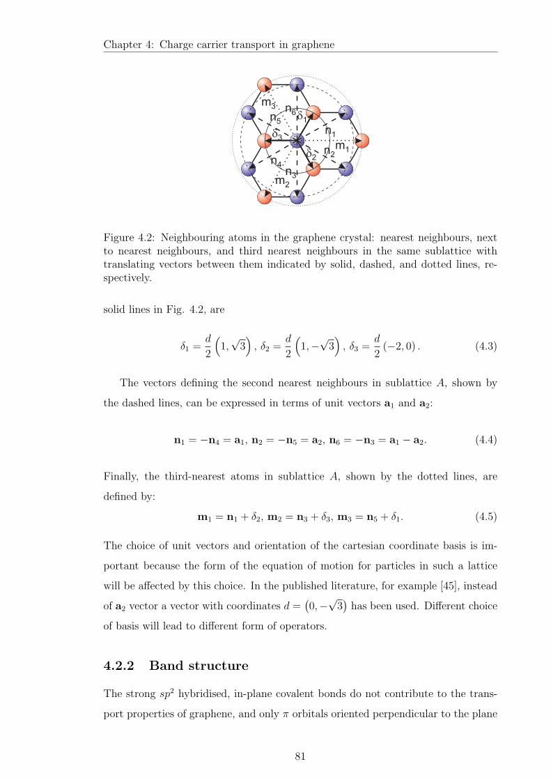
Chapter 4: Charge carrier transport in graphene
Figure 4.2: Neighbouring atoms in the graphene crystal: nearest neighbours, nextto nearest neighbours, and third nearest neighbours in the same sublattice withtranslating vectors between them indicated by solid, dashed, and dotted lines, re-spectively.
solid lines in Fig. 4.2, are
δ1 =d
2
(1,√
3)
, δ2 =d
2
(1,−
√3)
, δ3 =d
2(−2, 0) . (4.3)
The vectors defining the second nearest neighbours in sublattice A, shown by
the dashed lines, can be expressed in terms of unit vectors a1 and a2:
n1 = −n4 = a1, n2 = −n5 = a2, n6 = −n3 = a1 − a2. (4.4)
Finally, the third-nearest atoms in sublattice A, shown by the dotted lines, are
defined by:
m1 = n1 + δ2, m2 = n3 + δ3, m3 = n5 + δ1. (4.5)
The choice of unit vectors and orientation of the cartesian coordinate basis is im-
portant because the form of the equation of motion for particles in such a lattice
will be affected by this choice. In the published literature, for example [45], instead
of a2 vector a vector with coordinates d =(0,−√3
)has been used. Different choice
of basis will lead to different form of operators.
4.2.2 Band structure
The strong sp2 hybridised, in-plane covalent bonds do not contribute to the trans-
port properties of graphene, and only π orbitals oriented perpendicular to the plane
81

Chapter 4: Charge carrier transport in graphene
do so. In the tight-binding approximation the many-particle Hamiltonian (in the ab-
sence of magnetic field) for non-interacting quasiparticles, using up to third-nearest
neighbours (see Fig. 4.2), can be written as [51,52]
Htb = −t∑
ri∈ΛA
3∑j=1
a†(ri)b(ri + δj)− t∑
ri∈ΛB
3∑j=1
b†(ri)a(ri + RIδj)
−t′∑
ri∈ΛA
6∑j=1
a†(ri)a(ri + nj)− t′∑
ri∈ΛB
6∑j=1
b†(ri)b(ri + RInj)
−t′′∑
ri∈ΛA
3∑j=1
a†(ri)b(ri + mj)− t′′∑
ri∈ΛB
3∑j=1
b†(ri)a(ri + RImj), (4.6)
where RI is an operator of rotation by π radians, a†(a) is an electron creation
(annihilation) operator on site ri ∈ ΛA and b†(b) is that on site ri ∈ ΛB. Index j
changes from 1 to 3 for nearest neighbours and for third nearest neighbours and from
1 to 6 for third-nearest neighbours. Vectors δj, nj mj are defined by expressions
4.3, 4.4, 4.5, respectively. The parameters t, t′, t′′ represent the hopping energy
between first, second, and third nearest neighbours respectively, and they are equal
to 2.8 eV, 0.1 eV, 0.07 eV, respectively [53]. This Hamiltonian takes into account all
hops between nearest neighbours in the lattice, ignoring many other contributions
like disorder and smaller hopping energies for more distant sites.
We can introduce the Fourier transform of creation and annihilation operators
by the following formulae:
a†(ri) =1√N
∑
k
e−ik·ria†(k), a(ri) =1√N
∑
k
eik·ria(k),
b†(ri) =1√N
∑
k
e−ik·rib†(k), b(ri) =1√N
∑
k
eik·rib(k), (4.7)
where N is the number of sites in sublattice A or B. If we substitute Eq. 4.7 into
Eq. 4.6 we have
Htb = −∑
k
(a†(k) b†(k)
) φ′(k) φ(k) + φ′′(k)
φ∗(k) + φ′′∗(k) φ′∗(k)
a(k)
b(k)
,
(4.8)
82

Chapter 4: Charge carrier transport in graphene
where
φ(k) = t
3∑j=1
eik·δj , φ′(k) = t′6∑
j=1
eik·nj , φ′′(k) = t′′3∑
j=1
eik·mj . (4.9)
Here we have used the definition of the delta function
δ(k− k′) =1
N
∑ri∈ΛA
eik′ri−ikri .
Using Eq. 4.8 the dispersion relation ε(k) for the charge carriers is calculated from
the condition on the determinant
∣∣∣∣∣∣φ′(k) + ε(k) φ(k) + φ′′(k)
φ∗(k) + φ′′∗(k) φ′∗(k) + ε(k)
∣∣∣∣∣∣= 0. (4.10)
By solving this quadratic equation the energy of carriers is
ε1,2(k) = −<φ′(k)±√|φ(k) + φ′′(k)|2 −=φ′(k)2. (4.11)
where <φ′(k) and =φ′(k) are real and imaginary part of φ′(k), respectively. The
positive sign corresponds to the conduction band and negative to the valence band.
The latter expression can be simplified because imaginary part is cancels and the
final result for the dispersion relation is
ε1,2(k) = −φ′(k)±√|φ(k) + φ′′(k)|2.
A simpler approximation used in the literature, when |φ| ¿ |φ′| and |φ| ¿ |φ′′|, is
E1,2(k) = ±|φ(k)|. (4.12)
It takes into account the nearest neighbours only.
4.2.3 Effective Dirac equation
There are six points in the corners of Brillouin zone where the conduction band
touches the valence band, called Dirac points:
(0,± 4π
3√
3d
),
(2π
3d,± 2π
3√
3d
),
(−2π
3d,± 2π
3√
3d
). (4.13)
83

Chapter 4: Charge carrier transport in graphene
The dispersion relation is linear around these points. There are two inequivalent
Dirac points K+ =(0, 4π
3√
3d
)and K− =
(0,− 4π
3√
3d
), which we choose in the opposite
points in the first Brillouin zone defined as shown in Fig. 4.3. We can rewrite the
tight-binding Hamiltonian (4.8) for nearest neighbours in the vicinity of K+ and
K− points [54]as
Htb+1 ' hvF
∑
k
Ψ†K+(κ)
0 iκx + κy
−iκx + κy 0
ΨK+(κ), (4.14)
Htb−1 ' hvF
∑
k
Ψ†K−(κ)
0 iκx − κy
−iκx − κy 0
ΨK−(κ), (4.15)
where vF = 3td/2 is a Fermi velocity. If we consider all contributions from nearest
neighbours, the following expression will appear in the first order expansion of Eq.
4.8 for a single particle by a wavevector near the Dirac points K+, K−:
Htb±1 =
3t′ hv∗F (iκx ± κy)
hv∗F (−iκx ± κy) 3t′
, (4.16)
where the Fermi velocity is renormalised due to the presence of third neighbour
hopping integral t′′ as v∗F = 3d(t − 2t′′)/2, and ± indexes correspond to a specific
Dirac point K±. The second order expansion gives
Htb±2 =
−9
4d2t′(κ2
x + κ2y) α(κx ± iκy)
2
α(κx ∓ iκy)2 −9
4d2t′(κ2
x + κ2y)
, (4.17)
where α = 3ht(1 + 4t′′/t)d2/8. The diagonal terms of the Hamiltonian change the
position of the Fermi energy and break the symmetry between holes and electrons
can be absorbed in the chemical potential [51] as an additional term which shifts
the Fermi energy. These terms have circular symmetry and change slightly the
slope of the dispersion relation, but off-diagonal terms distort the spectrum and
are responsible for ’trigonal warping’ [55], so-called because of the triangular shape
of the Fermi surface. The resulting dispersion relations for electrons and holes are
84

Chapter 4: Charge carrier transport in graphene
Figure 4.3: Band diagram for graphene in the nearest neighbours approximationdescribed by Eq. 4.12. Two nonequivalent Dirac points (K− and K+) are shown.
given by the following expressions with second order in κ:
εK±e = 3t′ + hv∗F
√κ2
x + κ2y −
9
4d2t′(κ2
x + κ2y)±
ακy√κ2
x + κ2y
(3κ2x − κ2
y),
εK±h = 3t′ − hv∗F
√κ2
x + κ2y −
9
4d2t′(κ2
x + κ2y)∓
ακy√κ2
x + κ2y
(3κ2x − κ2
y).
4.2.4 Rotation
A rotation of the coordinate system in Fig. 4.1 by an angle η changes the form of
the Dirac equation, but should not change the dispersion relation. Thus, a phase
factor can be added to the Dirac Hamiltonian to account for this. Calculations show
that a single-particle Hamiltonian changes under rotation by an angle η as [55]
H± = hvF
0 e±iη(iκx ± κy)
e∓iη(−iκx ± iκy) 0
, (4.18)
From this Hamiltonian, other Hamiltonians used in literature can be obtained. For
example, it can be transformed to a most common form when the rotation by −π/2
is made [52]:
H = hvF
0 κx − iκy 0 0
κx + iκy 0 0 0
0 0 0 −κx + iκy
0 0 −κx − iκy 0
. (4.19)
85

Chapter 4: Charge carrier transport in graphene
where we exchange the sublattices A −→ B in the spinor for the K− Dirac point in
order to use a simple form for the Dirac equation
H±ψ± = ±hvF (σ1κ1 + σ2κ2)ψ± = εψ±, (4.20)
where σ1 and σ2 are Pauli matrixes and ψ± are spinor wavefunctions for the two
valleys.
4.2.5 Chirality
The wavefunctions for K± points can be found by solving equation (4.20) as
ψK±e =
1√2
1
± κx+iκy√κ2
x+κ2y
,
ψK±h =
1√2
±−κx+iκy√
κ2x+κ2
y
1
, (4.21)
where indexes e and h correspond to electrons and holes, respectively. One can
construct a pseudochirality operator [52] defined as
h =κxσx + κyσy√
κ2x + κ2
y
, (4.22)
which has a specific eigenvalue if it acts on the wavefunctions in Eq. (4.21). Namely,
hψK±e = ±ψK±
e , hψK±h = ∓ψK±
h , (4.23)
where electrons and holes have opposite sign eigenvalue (chirality) in both valleys.
Electrons have +1 chirality in the K+ valley and −1 chirality for the K− Dirac
point. Conservation of this quantum number plays an important role in transport
properties of quasiparticles in graphene discussed in the next section.
4.3 Transport properties
Graphene is a semiconductor with zero band gap. When the resistance of graphene
placed on top of SiO2 is measured as a function of gate voltage, a single peak of
86

Chapter 4: Charge carrier transport in graphene
large but finite resistance is observed. The Fermi energy (or gate voltage) at which
this peak occurs is called the Dirac or electroneutrality point. In ideal graphene
without doping the Fermi level should lie at the Dirac point (zero gate voltage) if
the dispersion relation is symmetric with respect to zero energy (crossing points).
This is correct only if transfer integrals to nearest neighbours are taken into account.
Doping shifts the Fermi level and thus the resistance peak from the zero gate voltage
position.
It has been observed experimentally that the resistance at the Dirac point is not
infinite (as one can expect because of zero concentration of free charge carriers) but
finite. Many samples have approximately the same resistivity in the Dirac point,
h/4e2. This can be due to layer of water formed during the mechanical cleavage. The
closeness of the value of the resistivity to h/4e2 in the Dirac point has suggested
it is a universal value [56]. However, it was recently shown that the amplitude
of the Dirac peak as well as mobility depends on doping and decreases [57] due to
scattering on Coulomb impurities. The amplitude of the peak is roughly independent
of temperature [58], but only in the case of graphene on Si/SiO2 substrate. Since
transport measurements of free standing graphene have been carried out, it has been
shown that the peak resistivity is not universal and has temperature dependence [59].
The Dirac point has more complications because at small carrier density graphene
becomes inhomogeneous due to disorder and electron-hole puddles are formed [60].
However, for transport properties in the diffusive regime not close to the Dirac
point, a standard Boltzmann transport equation is used [61]. The applicability of
the Boltzmann approach fails only close to the Dirac point where the wavelength
tends to infinity (because the energy goes to zero). Due to chirality of the carriers
in graphene the collision integral has to be revised, because this property prohibits
backscattering, as has been shown in all orders of perturbation theory by Ando [62].
The conductivity is given by the conventional formula
σ = neµ, (4.24)
where n is the concentration of mobile carriers, e is elementary charge, and mobility
µ is given by [21]
µ =ev2
F
εF
τ(εF ). (4.25)
87

Chapter 4: Charge carrier transport in graphene
The relaxation time τ(εF ) is given by the collision integral [61]
h
τ(εF )= 2π
∫d2κ′
(2π)2〈|Vκ,κ′|2〉(1− cos (θκ − θκ′))δ(εκ − εκ′), (4.26)
where θκ−θκ′ is an angle between incident κ and scattered κ′ wavevectors, δ(εκ−εκ′)
is the Delta function, and 〈|Vκ,κ′|2〉 is the average of the scattering potential matrix
element in momentum space over the distribution of scatters. The latter is changed
with the type of the defects that create the scattering potential. There are two
main defects in the lattice which are considered by theoreticians using the Born
approximation: short range disorder and Coulomb impurities [61].
Coulomb impurities are the most important source of scattering as they deter-
mine the constant mobility of graphene at high gate voltages (far from the Dirac
point) [61]. By replacing the Cartesian coordinate system with a polar one and
performing integration over energy in Eq. (4.26) we arrive at the expression
h
τ(εF )= 2πniD(εF )
∫ π
0
dθ
2π(1− cos (θ))(1 + cos (θ))
(2πe2
κqε(q)
)2
, (4.27)
where D(εF ) is density of states in graphene at the Fermi energy, ni is the concen-
tration of impurities (about 1012 cm−2 for thermally oxidised Si), q = 2ε/γ sin θ/2,
γ is the band parameter equal to 6.5 eV·A [61]. The factor (1 + cos (θ)) in the in-
tegral comes from the chirality of the particles which prohibits backscattering. The
latter integral can be evaluated and the conductivity due to scattering on Coulomb
impurities becomes
σ0 =e2
4π2h
n
ni
H0, (4.28)
where H0 is a constant, and n is carrier concentration. This expression is linear as
a function of carrier concentration and it shows that the mobility is independent of
concentration.
For short range scatterers the picture is completely different. A short range
impurity is the one that acts on a particle only in a range less than the carbon-
carbon distance and is near an A or B site in the crystal lattice. The presence of
such an impurity means that the electron has different energies when it localised on
A site or on B site and the conditions for the applicability of a continuum model
(Dirac equation) with independent Dirac points are not satisfied [62]. It has been
88

Chapter 4: Charge carrier transport in graphene
shown that the conductivity for short range scatterers is independent of energy [63].
Physically, this can be explained as follow. According to the Fermi’s golden rule
1/τ ∝ 〈|Vκ,κ′|2〉D(EF ), where D(EF ) ∝ E. Thus, the mobility is inversely propor-
tional to the carrier concentration, µ ∝ n−1 and the conductivity is independent of
the Fermi energy.
The total resistance can be viewed as a sum of two contributions: from scattering
on short range impurities ρS (lattice defects or screened Coulomb potential) and
long-range ρL (for example, nonscreened Coulomb potential). As soon as scattering
on Coulomb impurities is avoided (by suspending graphene over silicon dioxide) the
mobility can increase to 2 × 105 cm2 V−1 s−1 [59] because of the large intrinsic
mobility [58] related to internal (phonons) scattering processes. This large mobility
can be useful for production of ballistic structures to study some effects specific
to graphene. But there is another way to study ballistic transport in graphene,
by producing a sample that is small compared to the mean free path (or measure
transport in a small part of a larger sample) or producing a p-n junction.
4.3.1 p-n junction
A p-n junction can be created in a graphene flake by a top-gate. The top-gate can
change locally not only the conductance of graphene but also the type of carrier,
from electrons to holes or vice versa. By applying to the top-gate opposite to the
back-gate polarity under the top-gate one can have an electron region, while away
from the top-gate holes can be the charge carriers. Top gates have already been
made using a dielectric between the graphene flake and the gate [64–68].
Graphene is considered as a promising material for future electronic applications.
However, to replace the silicon technology graphene needs to overcome a serious
limitation. Because graphene is a semiconductor with zero band gap, the transistors
have leakage current and just producing top-gate is not enough to make a working
transistor. One of the possible ways to produce a band gap and reduce leakage is to
make a narrow ribbon about 10 nm width. In this case the spectrum of carries is
broken into several quantized subbands and a band gap between the lowest electron
subband and the highest hole subband is formed.
The type of dielectric between the top-gate and the graphene flake strongly
89

Chapter 4: Charge carrier transport in graphene
affects the mobility of the carriers [65]. If the mobility is small, ballistic effects will
be suppressed. One of the possible solutions of this problem is to avoid the use of a
dielectric but make a suspended top-gate [69].
Due to the chirality of carriers, transport through a p-n junction in graphene has
its own specifics. The case of a rapid change of the potential in the p-n junction is
discussed in [46]. It has also been shown that ballistic quasiparticles can penetrate
a p-n junction without reflection at zero angle of incidence. At other angles there
is a probability for carriers to be scattered back. This result has been extended to
any smooth potential including a linear one where the quasiclassical approximation
is applicable [43].
A p-n junction can be diffusive, when there are scatterers in the region of the p-n
junction or ballistic when there are no scatterers there. In the first case, to predict
the resistance of the p-n junction a diffusive transport model should be used. In
the diffusive transport model the probability of the carriers to penetrate through
the p-n junction is independent of the angle of incidence, but in the case of ballistic
transport the theory by [43] should be applied. Due to the reflection at other than
zero degree angles, the resistance of a ballistic p-n junction in graphene is larger
than a diffusive one. This excess resistance above the prediction of the diffusive
model in a graphene structure with a p-n junction was observed in [65].
4.3.2 Ballistic transport in a p-n junction
Cheianov and Fal’ko [43] have studied penetration of chiral particles through ballistic
p-n junctions with a linear energy barrier as a function of coordinate x (in the current
direction):
u(x) = Fx, (4.29)
where F is an energy gradient. F is the main parameter which affects the transmis-
sion coefficient through the p-n junction and thus its resistance.Ballistic transport
through p-n junction means that electrons which approach the boundary of a p-n
junction penetrate from the p region into the n region without scattering on impu-
rities or defects. If the particle has a nonzero κy wave vector-component, there is
a region of classically unreachable space which the particle can penetrate only via
tunnelling (see Fig. 4.4). The total energy of electrons (with the assumption that
90
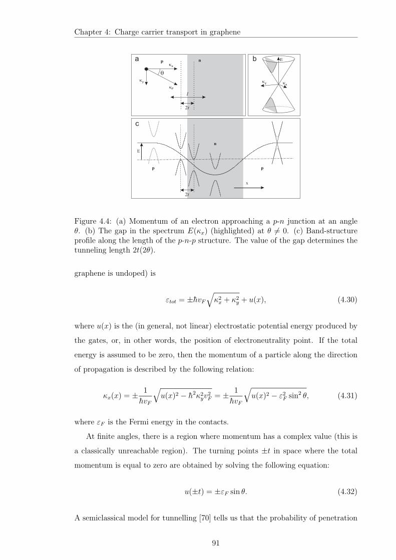
Chapter 4: Charge carrier transport in graphene
Figure 4.4: (a) Momentum of an electron approaching a p-n junction at an angleθ. (b) The gap in the spectrum E(κx) (highlighted) at θ 6= 0. (c) Band-structureprofile along the length of the p-n-p structure. The value of the gap determines thetunneling length 2t(2θ).
graphene is undoped) is
εtot = ±hvF
√κ2
x + κ2y + u(x), (4.30)
where u(x) is the (in general, not linear) electrostatic potential energy produced by
the gates, or, in other words, the position of electroneutrality point. If the total
energy is assumed to be zero, then the momentum of a particle along the direction
of propagation is described by the following relation:
κx(x) = ± 1
hvF
√u(x)2 − h2κ2
yv2F = ± 1
hvF
√u(x)2 − ε2
F sin2 θ, (4.31)
where εF is the Fermi energy in the contacts.
At finite angles, there is a region where momentum has a complex value (this is
a classically unreachable region). The turning points ±t in space where the total
momentum is equal to zero are obtained by solving the following equation:
u(±t) = ±εF sin θ. (4.32)
A semiclassical model for tunnelling [70] tells us that the probability of penetration
91

Chapter 4: Charge carrier transport in graphene
through a long and high potential barrier is described by the expression
wexactpn (θ) ∼ e−2S/h = exp
(−2
∫ l
−l
|κx(x)|dx
). (4.33)
Here S is action. In general, the probability has to be small compared to unity to
make this quasiclassical model applicable, but Cheianov and Fal’ko have proved,
using a transfer matrix formalism, that this formula with a coefficient calculated
can be used to obtain the total angular dependance of probability of tunnelling.
Conductance of the p-n junction per unit width is given by
Gnp =4e2
h
∫dκy
2Wπwexact
pn (θ) =4e2
h
∫WkF cos θdθ
2πwexact
pn (θ), (4.34)
where W is the width of the sample. For small angles (where the transmission is
not small) Eq. 4.34 can be simplified and the conductance of a p-n junction can be
calculated analytically (by integrating over the range of θ from −∞ to +∞):
Gnp =2e2
πhW
√F
hvF
. (4.35)
One can see that the conductance is independent of the Fermi energy. In a real
sample, to see ballistic transport through a p-n junction we have to have the mean
free path l larger than tunnelling distance 2t, as shown in Fig. 4.4(a). An effective
band gap appears if the quasiparticle approaches the p-n junction at a non-zero
angle, due to a finite y component of the wavevector, Fig. 4.4(b). In this case there
is a region of the p-n junction where the quasiparticle has an imaginary wavevector:
this region has length 2t and depends on angle θ (Fig. 4.4(c)).
4.3.3 Ballistic transport in a p-n-p junction
Katsnelson [46] has discussed ballistic transport through a rectangular potential bar-
rier in graphene. It was predicted that a particle approaching with normal incidence
to a rapid barrier has perfect transmission, without backscattering for any height of
the barrier. This has an analogy in high-energy physics called ”the Klein paradox”.
The effect has not yet been observed experimentally.
The model of transport through a rectangular barrier is formed on the basis
92

Chapter 4: Charge carrier transport in graphene
Figure 4.5: Total transmission as a function of height of a rectangular barrier. (a)Different lengths of the barrier, using Eq. (4.40) for a single channel. Energy ofelectrons ε=0.06 eV. The model potential u(x) is shown in the top left inset. (b)Influence of the finite width of the ribbon for 50 nm barrier length. T tot for a singlechannel, 100 nm, and 200 nm width is presented.
of a low energy effective Dirac Hamiltonian (Eq. 4.19). The barrier region with
potential of height V0 should have a Hamiltonian with an additional term: namely,
the Hamiltonian for the K+ valley with an external potential u(x) can be written
as:
H = −ihvF σ · ∇+ u(x), (4.36)
where h is Plank’s constant, vF is Fermi velocity, σ = (σx, σy) is a vector consisting of
Pauli matrixes, and ∇ = (∇x,∇y) is a gradient operator. The potential is different
for the three regions shown in the inset in Fig. 4.5(a):
u(x) =
V0, 0 < x < D, region II
0, otherwise, regions I and III
.
Let D be the width of the barrier and ε the energy of a particle. Then if we
divide the space of the problem into three regions, we can write the solution of Dirac
equation for each region as
ψI(r) =1√2
1
seiφ
ei(kxx+kyy) +
r√2
1
sei(π−φ)
ei(−kxx+kyy), (4.37)
93

Chapter 4: Charge carrier transport in graphene
ψII(r) =a√2
1
s′eiθ
ei(qxx+kyy) +
b√2
1
s′ei(π−θ)
ei(−qxx+kyy), (4.38)
ψIII(r) =t√2
1
seiφ
ei(kxx+kyy), (4.39)
where φ = arctan (ky/kx), θ = arctan (ky/qx), and wavevectors in the region I and
III are equal to kx = kF cos φ, ky = kF sin φ, for the region II under the barrier the
wavevector is qx =√
(V0 − ε)2/v2F − k2
y, s = sign(ε) and s′ = sign(ε−V0). There are
two unknown coefficients, r and t, which should be determined from the conditions
of continuity of the wave function at the boundaries of the rectangular potential. By
solving this problem the expression for the transmission probability as a function of
angle is calculated [53] as
T (φ) =cos2 θ cos2 φ
[cos (Dqx) cos φ cos θ]2 + sin2 (Dqx)[1− ss′ sin φ sin θ]2. (4.40)
Using this expression, the dependence of transmission on the height of barrier has
been plotted in Fig. 4.5(a). The form of the transmission for a single channel has
an oscillatory behavior as a function of height of the barrier, which follows from the
interference of transmitted and reflected waves within the barrier. In Fig. 4.5(a)
three lengths of the barrier are shown to demonstrate that the period of oscillations
as well as their amplitude decrease with increasing length. However, for a narrow
sample the calculation of the transmission should be revised because of the finite
number of propagating modes. The component of the wavevector parallel to the
barrier takes only quantised values which are determined by the width of the sample
and boundary conditions for an ideal ribbon [71]. The values are
κn =
(n +
1
2
)π
W, n = 0, 1, 2, ..., (4.41)
where W is width of the sample. Thus, the total conductance is calculated from
the sum of the transmission probabilities of individual modes with wavevectors less
94

Chapter 4: Charge carrier transport in graphene
than the Fermi wavevector
G =4e2
hT tot =
4e2
h
N−1∑n=0
Tn, (4.42)
where N is total number of propagating modes. If we consider a finite width of the
ribbon, for example, 100 nm or 200 nm (see Fig. 4.5(b)), the relative amplitude of
the oscillations is conserved. The variation of the resistance is about 20 %.
In section 4.4.4, we will use this model for comparison with an experiment which
has been performed on top-gate graphene structures.
4.4 Experiment and analysis
4.4.1 Overview of the experimental results
The data and analysis for three two-terminal graphene samples with ’air-bridge’
top-gates are presented. The samples were fabricated by Roman Gorbachev from
the laboratory of Quantum Transport in Nanostructures at Exeter University using
the technology discussed in Section 2.2.3. Details of these samples are given in Table
4.1. The third sample S3 has been measured by the author and the data for the first
and second samples (S1 and S2 respectively) are provided by Roman Gorbachev.
The resistivity dependence on back-gate voltage for these three samples is shown in
Fig. 4.6(a). The samples have different mobilities, and it was expected that the first
sample, with the largest mobility, has to show some features of ballistic transport
through a p-n junction formed by the top-gate. (In this sample the mean free path
becomes comparable to the gate length.)
The top-gate dependence at fixed back-gate voltages for the three studied sam-
ples are shown in Fig. 4.6(b-d). On the same graphs the expected resistance as a
function of top-gate voltage is shown assuming purely diffusive transport dominates
(see Section 4.4.2). The difference between experiment and predictions are clearly
seen on the graphs.
We attribute the difference between experiment and diffusive theory to the bal-
listic transport through the two p-n junctions (but not through the whole p-n-p
structure) formed by the top-gate. To calculate the expected value for the resis-
95

Chapter 4: Charge carrier transport in graphene
Figure 4.6: (a) Resistivity of the three samples as a function of the back-gate voltage,at Vtg = 0, at T = 50 K. Points indicate the values of Vbg where the top-gate voltagewas swept to produce p-n-p junctions. (b) The resistance of sample S1 as a functionof top-gate voltage at different Vbg. (c,d) The resistance as a function of top-gatevoltage at different Vbg of samples S2 and S3, respectively. Points show the results ofthe calculations of the expected resistance assuming diffusive transport of carriers.(Dashed lines in b,c are guides to the eye.)
tance of a single p-n junction we have used theory [43] as described earlier (4.3.2).
This resistance is determined by the energy gradient F in the middle of the junction.
To find the energy profile, the density of states in graphene should be taken into
account. This has been done by solving the 2D electrostatic problem with correct
boundary conditions on graphene, as discussed in Section 4.4.2. The results of these
calculations are presented in Table 4.1 (last two entries).
96

Chapter 4: Charge carrier transport in graphene
Characteristics S1 S2 S3Width, µm 0.3-0.15 0.6 0.15Length, µm 5 4.3 1.45Dirac point, V 0.05 1.11 1.68Resistivity in Dirac point, kOhm 6.9 4.87 6.36Mean free path, nm 100 75 45Top-gate length, nm 170 170 100Top-gate distance, nm 140 210 130Resistance difference, kOhm 3.8 (-9 V) -1.82 (-4 V) 0 (-14 V)Efficiency of top-gate 0.35 0.24 0.4Energy gradient, eV/m 1.5 · 106 0.8 · 106 2.4 · 106
Mobility, cm2V−1s−1 (n=3·1011 cm−2) 12.5 11 6-7Fermi wave vector, 107 m−1 6.5 3.4 5.87Fermi energy, eV 0.043 0.0225 0.038Fermi wavelength, nm 96 188 109Critical angle ∼ 25 ∼ 25 ∼ 30Critical tunnelling distance ∼ 40 ∼ 40 ∼ 40Number of modes 7 11 3Resistance, kOhm (diffusive model) 2.17 0.62 1.85Resistance, kOhm (Cheianov model) 3.6 1.95 4.4
Table 4.1: Parameters of graphene samples with ’air-bridge’ top-gates.
For sample S3, the resistance as a function of back and top-gate voltage, temper-
ature and magnetic field has been measured (see Fig. 4.7). The colour scale (4.7(a))
indicates the efficiency of the top-gate (how the energy changes with voltage) by
the slope of the dashed line, which shows the position of the peak in the resistance
corresponded to formation of two p-n junctions. The efficiency is equal to 0.4, which
makes the distance between the flake and top-gate found by modelling (for details
see Section 4.4.2) the smallest out of the three samples. This creates the narrowest
p-n-p junction in graphene. To see how ballistic the junction is, we need to estimate
the mean free path. Using the standard formula for conductivity
σ =2e2
hκF l, (4.43)
and taking into account that κF = εF /hvF = ±31 meV√|Vbg|/hvF (where Vbg is
given in V) the mean free path
l = 2.7 · 10−4 σ√|Vg|([m]). (4.44)
97

Chapter 4: Charge carrier transport in graphene
0 10 20 30 40 5020
25
30
35
40
-15 -10 -5 0 5 100.1
0.2
0.3
0.4
0.5
0.6
40
60
80
100
0 10 20 30 40 5020
30
40
50
60
T = 27 K
T = 80 K
Vtg, V
R, k
Vbg = -5 V
T = 50 K
-10 -8 -6 -4 -20
10
20
30
40
50R, k
p-p-p
Vbg, V
p-n-p
Vtg, V
18
24
31
38
44
51
d
ca
Vbg, V
S3
l, nm, mS
400 / m
200 / m
b
T = 80 KVbg = -5 V
Vtg, VR
, k
0 T -1 T -2 T -3 T -4 T -5 T 0 T
Figure 4.7: Sample S3. (a) Colour-scale of the resistance as a function of top-gatevoltage and back-gate voltage at T=50 K. The dashed line shows the position of theDirac point under the top-gate and separates the p-p-p region from the region wherethe p-n-p junction is formed. (b) Conductivity and mean free path as a function ofback-gate voltage at T = 50 K. The mean free path is calculated for two differentcontact resistances 200 Ω/µm and 400 Ω/µm. (c) Temperature dependence of theresistance fluctuations as a function of top-gate voltage. (d) Resistance as a functionof top-gate voltage at T = 80 K for different magnetic fields perpendicular to theflake. The orange curve shows reproducibility of the result.
In Fig. 4.7(b) the conductivity and mean free path as a function of back-gate volt-
age for different contact resistances are shown. (Here the Dirac point is shifted to
zero back-gate voltage.) The total measured resistance also includes the contact
resistance between the flake and the two ohmic contacts. This contact resistance
should be subtracted before calculation of the mean free path. Typical values of
200 Ω/µm for two-terminal graphene samples have been determined by comparison
of the values of the resistance in quantum Hall plateaux with the expected ones [24].
The mean free path of sample S3 is smaller than that of S1 and S2 and is equal to
45 nm for the electron region and 50 nm for the hole region. It decreases slightly
with decreasing back-gate voltage, but increases dramatically near the Dirac point
due to the divergence which occurs at zero concentration. (In reality the concentra-
98

Chapter 4: Charge carrier transport in graphene
tion of the carriers in the Dirac point is not zero, because of strong inhomogeneity
and formation of electron-hole puddles [60], hence the simple formula (4.43) is not
applicable in this region.) Thus, the increase of the mobility near the Dirac point
can be an artefact of using incorrect relation.
In Fig. 4.7(c) the resistance as a function of top-gate voltage is presented for three
temperatures (27 K, 50 K, 80 K). The first peak appears at Vtg = 13 V, when two p-n
junctions are formed. The resistivities of the two p-n junctions are higher than that
in other regions of the structure – this is the reason for the resistance increase. If the
top-gate voltage increases further, no big change of the resistance of the structure
at the formation of p-n junctions is seen. In this Vtg-range the resistance has shown
reproducible fluctuations as a function of top-gate voltage. These fluctuations have a
smaller ”period” and larger amplitude at low temperatures. We can suggest several
reasons for these fluctuations. The first is mesoscopic resistance fluctuations, as seen
in normal small MOSFET samples at low carrier densities [29]. The second reason
is a variation of unintentional doping in the flake which results in different position
of the Dirac point under the top-gate. In this case each resistance peak corresponds
to different Dirac points. Non-uniformity of the structure can be caused by non-
uniformity of the top-gate itself. Instead of a constant height across the flake, the
gate can contain areas with different distances from the flake. Then, even if the
2D gas is homogenous, the efficiency of different parts of the top-gate becomes a
function of x-coordinate. The third reason is ballistic transport through the whole
p-n-p structure which can produce oscillations in the resistance as a function of
top-gate voltage. This latter reason can be only applicable near the onset of p-n-p
structure where the length of the n-region can be comparable to the mean free path.
In Fig. 4.7(d) the resistance as a function of top-gate voltage at Vbg = −5
V measured at T = 80 K is shown for different fixed magnetic fields up to 5 T.
It is seen that the positive magnetoresistance is significantly stronger at large Vtg
when a p-n-p structure is formed. We attribute this magnetoresistance to geometric
magnetoresistance discussed in Section 4.4.5.
In the following subsections we introduce our electrostatic model and apply the
theory of ballistic transport through p-n and p-n-p junctions to explain the experi-
mental results.
99

Chapter 4: Charge carrier transport in graphene
4.4.2 Electrostatic model
To find the resistance of a graphene flake at any voltage applied to the back-gate
and top-gate we have to know the distribution of the electrostatic potential along
the flake. Then, using the known relation between this potential and the back-gate
voltage, we can find the resistivity at a point along the flake for a specific value of
electrostatic energy. Finally, assuming a simple diffusive model, we can integrate
the resistivity over the length to obtain the total resistance of the sample or any
part of the p-n-p structure.
Solution of 3D electrostatic problem is complicated and time consuming, and we
have chosen a simple 2D model for our numerical calculations. We have assumed
that the sample has infinite size in the direction perpendicular to the current. This
assumption should not affect the final result as long as edge effects can be neglected.
The 2D coordinate system has the coordinate x along the length of the sample in
the direction of the current flow and z is the vertical coordinate perpendicular to
the flake.
The geometry of the electrostatic model is shown in Fig. 4.8. The total region of
the calculations is taken to be large enough to exclude the influence of the boundary
conditions at the outer boundaries: in this case the potential in the flake does not
depend on the boundary conditions on the ”box”. The length of the calculated
region is 25 µm and its height is 6 µm. (It was tested that the main result does not
change if we increase the ”box” by two times or take other than periodic boundary
conditions.) The length of a graphene flake placed in the middle of the region is 5
µm for the first sample, 4.3 µm for the second sample, and only 1.45 µm for the
third sample: this is much smaller than the size of the ”box”. The typical distance
from the flake to the top-gate is about 200 nm (see Table 4.1). The geometry shown
in Fig. 4.8(a) is for S2 sample where the distance from the flake to the top-gate is
250 nm. The metallic top-gate in Fig. 4.8(b) is shown as a rectangle with constant
potential along the boundaries. The flake has been modeled as a line placed on top
of a SiO2 substrate of 300 nm thickness, with specific boundary conditions discussed
below.
We have solved the Laplace equation,4φ = 0, in 2D (xz-plane), with a numerical
package FEMLAB, which uses a finite-element method to solve 2D problems. The
100

Chapter 4: Charge carrier transport in graphene
Figure 4.8: Electrostatic model used to find the distribution of potential in agraphene flake. It uses real size geometry and correct boundary conditions forgraphene (see Eqs. (4.45) and (4.46)). (a) Whole geometry of the model, (b) Zoom-in region under the top-gate. An additional layer of impurities is shown by thedotted line.
code has been used to obtain the distribution of electrostatic energy in the graphene
flake as a function of the x-coordinate by calculating the potential along the line
of the graphene flake. This code is given in Appendix 6. We have set potentials
on the back and top-gates to reproduce experimental conditions. The graphene
flake was modeled using charge surface density boundary conditions, assuming that
the temperature is zero. The displacement field has to have a discontinuity on the
graphene flake:
n · (D1 −D2) = ρs, (4.45)
where n is a unit vector normal to the graphene surface, D1 and D2 are displacement
field vectors above and below the flake, and ρs is charge density defined as
ρs = −e
∫ eφ
0
gsgv
2πh2v2F
εdε = − gsgve3
2πh2v2F
φ2
2sign(φ), (4.46)
101

Chapter 4: Charge carrier transport in graphene
where sign(φ) determines the sign of the potential (sign(φ) = 1 if φ > 0, otherwise
sign(φ) = −1), gs is the spin degeneracy, and gv is the valley degeneracy. The charge
cannot move (there is no current) but is allowed to redistribute in a self-consistent
way over the flake. The carrier concentration can then be written as
n = gsgv
∫dκxdκy
(2π)2= gsgv
∫2πκdκ
(2π)2=
∫gsgv|ε|2πh2v2
F
dε. (4.47)
In this relation, the density of states gsgv|ε|/2πh2v2F for graphene is used – it is linear
as a function of energy and disappears at zero energy.
The resistance as a function of back-gate voltage gives the dependance of resis-
tivity on potential in the graphene flake, ρ(φ), if the relation between φ and Vbg is
known. As soon as we know the potential distribution in the graphene flake obtained
from the modelling, the resistance of any part or whole structure can be found by
integration of the resistivity ρ(φ(x)) over the flake length. We used for calibration
the experimental resistance dependence on back-gate voltage to find ρ(φ(x)). The
calibration curve has been fitted by a piecewise polynomial function to get an an-
alytical expression which later has been used in numerical integration. Thus, the
resistance as a function of top-gate voltage at different fixed back-gate voltages can
be obtained from the integral
R =
∫ L
0
ρ(φ(x))dx. (4.48)
The position of the Dirac point in the three samples is shifted from zero Vbg
(see 4.6(a)) due to unintentional doping. In our calculations we assumed that the
Dirac point is at zero back-gate and top-gate voltages, by shifting the whole curve,
but adding a layer of charged impurities above the flake to the model has helped
to introduce the Dirac peak shift seen in experiment. (The shift of the Dirac point
occurs due to doping and the value of the shift gives us the concentration of these
impurities.) The charged impurities induce the same charge but of opposite sign is
added to the flake. The resistance dependence on back-gate voltage is reproduced
exactly by the model with this impurity layer. We have found that there is no
difference in R(Vbg) if the layer position is shifted from 1 nm to 10 nm above the
graphene flake.
102
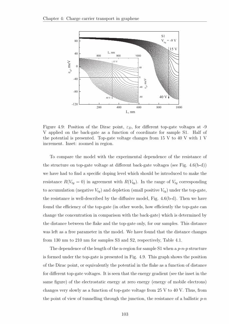
Chapter 4: Charge carrier transport in graphene
Figure 4.9: Position of the Dirac point, εD, for different top-gate voltages at -9V applied on the back-gate as a function of coordinate for sample S1. Half ofthe potential is presented. Top-gate voltage changes from 15 V to 40 V with 1 Vincrement. Inset: zoomed in region.
To compare the model with the experimental dependence of the resistance of
the structure on top-gate voltage at different back-gate voltages (see Fig. 4.6(b-d))
we have had to find a specific doping level which should be introduced to make the
resistance R(Vtg = 0) in agreement with R(Vbg). In the range of Vtg corresponding
to accumulation (negative Vtg) and depletion (small positive Vtg) under the top-gate,
the resistance is well-described by the diffusive model, Fig. 4.6(b-d). Then we have
found the efficiency of the top-gate (in other words, how efficiently the top-gate can
change the concentration in comparison with the back-gate) which is determined by
the distance between the flake and the top-gate only, for our samples. This distance
was left as a free parameter in the model. We have found that the distance changes
from 130 nm to 210 nm for samples S3 and S2, respectively, Table 4.1.
The dependence of the length of the n-region for sample S1 when a p-n-p structure
is formed under the top-gate is presented in Fig. 4.9. This graph shows the position
of the Dirac point, or equivalently the potential in the flake as a function of distance
for different top-gate voltages. It is seen that the energy gradient (see the inset in the
same figure) of the electrostatic energy at zero energy (energy of mobile electrons)
changes very slowly as a function of top-gate voltage from 25 V to 40 V. Thus, from
the point of view of tunnelling through the junction, the resistance of a ballistic p-n
103
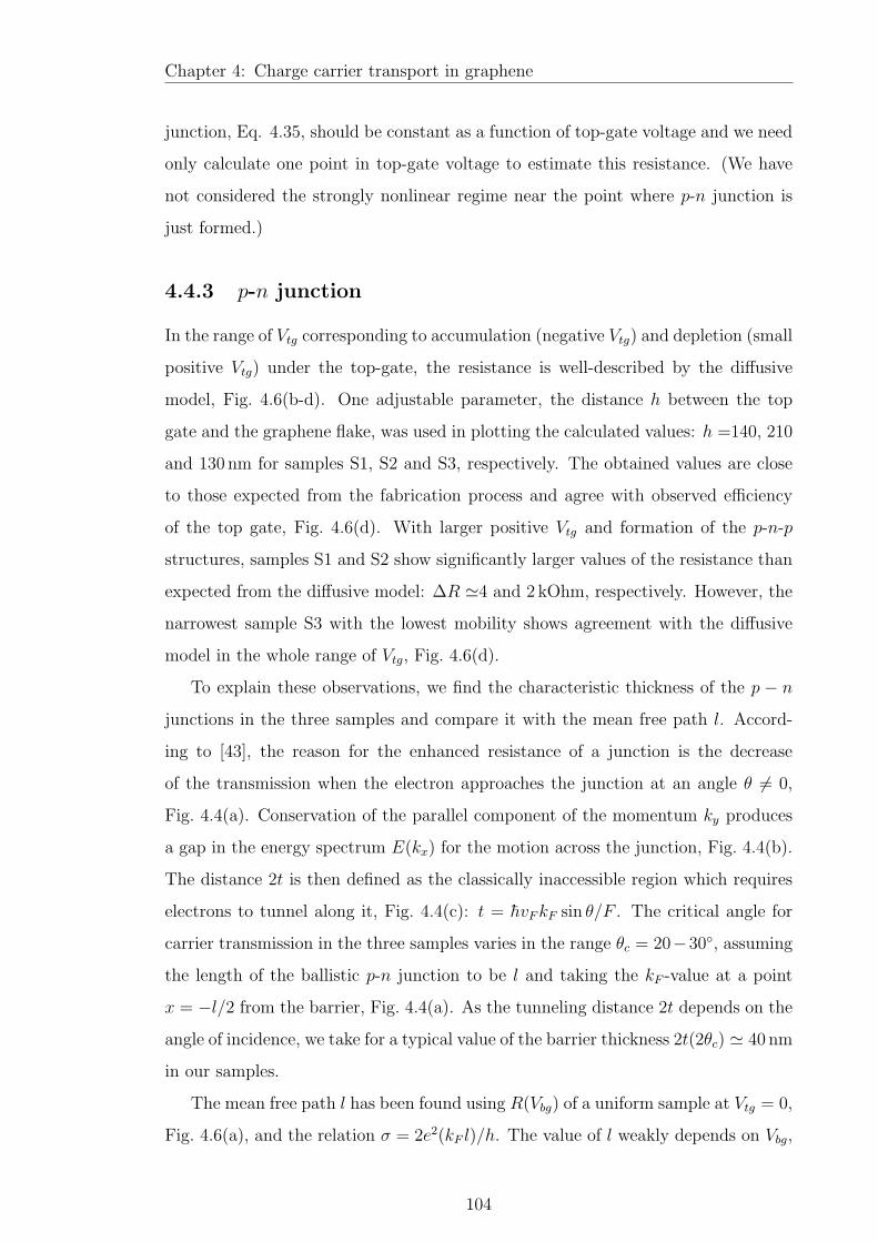
Chapter 4: Charge carrier transport in graphene
junction, Eq. 4.35, should be constant as a function of top-gate voltage and we need
only calculate one point in top-gate voltage to estimate this resistance. (We have
not considered the strongly nonlinear regime near the point where p-n junction is
just formed.)
4.4.3 p-n junction
In the range of Vtg corresponding to accumulation (negative Vtg) and depletion (small
positive Vtg) under the top-gate, the resistance is well-described by the diffusive
model, Fig. 4.6(b-d). One adjustable parameter, the distance h between the top
gate and the graphene flake, was used in plotting the calculated values: h =140, 210
and 130 nm for samples S1, S2 and S3, respectively. The obtained values are close
to those expected from the fabrication process and agree with observed efficiency
of the top gate, Fig. 4.6(d). With larger positive Vtg and formation of the p-n-p
structures, samples S1 and S2 show significantly larger values of the resistance than
expected from the diffusive model: ∆R '4 and 2 kOhm, respectively. However, the
narrowest sample S3 with the lowest mobility shows agreement with the diffusive
model in the whole range of Vtg, Fig. 4.6(d).
To explain these observations, we find the characteristic thickness of the p − n
junctions in the three samples and compare it with the mean free path l. Accord-
ing to [43], the reason for the enhanced resistance of a junction is the decrease
of the transmission when the electron approaches the junction at an angle θ 6= 0,
Fig. 4.4(a). Conservation of the parallel component of the momentum ky produces
a gap in the energy spectrum E(kx) for the motion across the junction, Fig. 4.4(b).
The distance 2t is then defined as the classically inaccessible region which requires
electrons to tunnel along it, Fig. 4.4(c): t = hvF kF sin θ/F . The critical angle for
carrier transmission in the three samples varies in the range θc = 20−30, assuming
the length of the ballistic p-n junction to be l and taking the kF -value at a point
x = −l/2 from the barrier, Fig. 4.4(a). As the tunneling distance 2t depends on the
angle of incidence, we take for a typical value of the barrier thickness 2t(2θc) ' 40 nm
in our samples.
The mean free path l has been found using R(Vbg) of a uniform sample at Vtg = 0,
Fig. 4.6(a), and the relation σ = 2e2(kF l)/h. The value of l weakly depends on Vbg,
104

Chapter 4: Charge carrier transport in graphene
and when extrapolated to the Dirac point (Vbg = 0 for an undoped sample) gives
l ' 100, 75 and 45 nm, respectively, for samples S1, S2 and S3. Comparing the
tunnelling length with the mean free path shows that the p-n junctions in S1 and S2
are ballistic (l À 2t), while in S3 they are less ballistic (l ∼ 2t). This can explain the
agreement of the resistance of S3 with the result of the diffusive model in Fig. 4.6(d).
To find the expected resistance Rpn of ballistic p-n junction in samples S1 and
S2 and compare it with the observed difference ∆R in Fig. 4.6, we first assume a
smooth potential barrier, 2kF t À 1, and by using the calculated value of electric
field F we get the tunneling probability wnp(θ) from
wnp(θ) = e−πhvF κ2y/F . (4.49)
Equation 4.35 is then used to obtain the resistance of the ballistic p-n junction. We
have found that using summation rather than integration is more appropriate in
our case, as samples S1 and S2 have less than 12 modes (the narrowest sample S3
has only three modes). The value of the Fermi momentum kF in these calculations
is taken at a distance l/2 from the barrier using the values of the mean free path
found above; however, the result for Rpn hardly changes if the value of l is varied by
two times either way. This is clear as the tunneling probability wnp(θ) in Eq. 4.49
depends only on ky which takes specific, quantised values ky = πn/W . The obtained
values are Rpn =5 and 2 kOhm for samples S1 (at Vbg = −9V, Vtg = 40V) and S2
(at Vbg = −4V, Vtg = 30 V).
Taking into account the Fermi wavelength at the distance l/2 from the barrier,
we see that 2kF t '2 for the three samples. To examine the applicability of a smooth-
barrier approximation for this (not too large) value of 2kF t, we have calculated w(θ)
directly using numerical methods [72] and compared the result with that obtained
from Eq. 4.49. It shows less than 5% difference from the value of Rpn calculated
above.
In experiment, it is not the resistance of an individual ballistic p-n junction
which is measured but the resistance of the whole p-n-p structure. It can be different
depending on whether its middle, n-region is long or short compared with l (i.e.,
diffusive or ballistic). For a diffusive n-region with three independent contributions
(two junctions and middle region) Rpnp ≥ 2Rpn, while for a ballistic n-region, Rpnp '
105

Chapter 4: Charge carrier transport in graphene
Rpn [43]. The resistance of a ballistic p-n-p structure should not increase with
addition of another junction as the electrons approaching the second junction have
already been selected by the first junction within the critical angle θc. Therefore,
they all will have high transmission probability wnp(θ) going through the second
junction.
Fig. 4.6(b,c) shows clearly that the resistance of S1 and S2 is larger than that
expected in the diffusive model by ∆R, because of the ballistic transport of chiral
carriers through two p-n junctions. To find their resistance, we assume that they
are independent; that is, the n-region is diffusive. Then the observed difference
∆R = 2(Rpn−RDpn), where RD
pn is the resistance of the diffusive p-n junction on the
length l which was taken into account in the diffusive-model calculation shown in
Fig. 4.6. With the values l =100 and 75 nm, one finds that RDpn =2 and 0.6 kOhm
for samples S1 and S2, respectively. This gives the corresponding resistance of
the ballistic p-n junction Rpn =4 and 1.6 kOhm, which is close to the expected
values of 5 and 2 kOhm. (Even better agreement, within 10%, is achieved if another
quantisation rule for graphene is used [71]: ky = π(n + 1/2)/W , n = 0, 1, 2, . . .)
The assumption of the diffusive nature of the n-region at large Vtg is confirmed by
Fig. 4.9, where the whole p-n-p region is seen to be larger than the mean free path.
However, near the onset of the p-n junctions, at small Vtg, the p-n-p region is much
shorter and can be fully ballistic.
We now discuss the applicability of Eq. (4.49) for the real potential. Using Eq.
4.31 we can rewrite Eq. 4.33 as
wexactpn (θ) = exp
(− 2
vF h
∫ l
−l
√|u(x)2 − ε2
F sin2 θ|dx
)(4.50)
where u(x) is the real electrostatic potential energy plotted in Fig. 4.9. In Fig.
4.10 we compare the momentum as a function of distance for the real potential and
the linear approximation. Because the dependence of the probability on angle θ is
sharp, there is a small difference (within 1 %) between the exact probability and
the approximations.
106

Chapter 4: Charge carrier transport in graphene
Figure 4.10: Comparison of exact and approximated potential momentums. Thereal part of momentum (px =
√ε2
F sin2 θ − u(x)2/vF ) as a function of coordinate atdifferent angles of incidence from 5 to 45 is presented. The red dashed curvesare calculated using linear approximation of potential. The most important parts ofthe momentum which make the main contribution to the probability are positionedin the region of 2t. This region is around the middle of the p-n junction (505 nm).
4.4.4 p-n-p junction
We now consider the resistance oscillations which we observed in sample S1. The
mean free path for sample S1 is 100 nm. This is much smaller than the width of
the middle n-region in the p-n-p junction formed by the top-gate as shown in Fig.
4.9 which is about 400 nm. As transport can still be ballistic at the onset of p-
n-p structure, we can speculate about the expected magnitude and period of the
resistance oscillations. We have used the function qtrans3 (listing is given in App.
6) written by F. Guinea, which calculates the probability of passing through a p-n-p
junction at some angle. This code works for any strong or sharp potential. The
results of calculations for sample S1 at Vbg = −9 V and Vtg varying from 19 V to 40
V are shown in Fig. 4.11. For the calculations 20 modes were used. The period of
these oscillations is about 1.3 V which is about 3 times smaller than those observed
in experiment. The amplitude of the oscillations is 0.4 kOhm, which is also smaller
than experimental value of 1-5 kΩ. To observe oscillatory behavior of the resistance
originating from the interference of electron waves within the n-region as a function
of top-gate voltage we need a much shorter n-region, which can be done only if the
top-gate width is shorter than 100 nm and the distance between this gate and the
flake smaller than 100 nm.
107
Chapter 4: Charge carrier transport in graphene
20 24 28 32 36 40
0.6
0.8
1.0
1.2
1.4
Vtg, V
S1V
bg = -9 V
p-n-
p ju
nctio
n re
sist
ance
, k
Figure 4.11: Oscillation of the resistance as a function of top-gate voltage for S1sample for discreet valuers of the wavevector. Vbg = −9 V.
4.4.5 Magnetoresistance of p-n-p structure
In Fig. 4.7(d) top-gate dependences of the resistance at different magnetic fields
for sample S3 are presented. It is seen that the magnetoresistance is approximately
linear as a function of magnetic field, which can be due to geometric magnetoresis-
tance as it expected to be linear at high magnetic fields [73]. The geometry of the
sample has to be taken into account, when a region with different types of carrier is
formed under the top-gate. When the sample has three regions connected in series:
left p-region, central n-region, and right p-region, the magnetoresistance increases
because the central “sample” is shorter than the whole structure (where geometric
resistance is the smaller). Sample S3 has not been studied in detail.
To study the effect of magnetic field on the resistance of p-n-p, a structure
diffusive sample S5 has been used, Table 2.3. Fig. 4.12(a) shows the resistance
as a function of back-gate voltage at T = 50 K(Vtg = 0 V). The Dirac point is
at Vbg = −0.75 V. This R(Vbg) dependence has been used to find the separation
between the top-gate and graphene layer. The measurements of the resistance as
a function of Vtg at Vbg = −9 V show good agreement with our diffusive transport
modelling, Fig. 4.12(b).
108

Chapter 4: Charge carrier transport in graphene
The resistance as a function of magnetic field, B, has been measured at differ-
ent back-gate voltages, Fig. 4.13(a). The magnetoresistance at different Vbg as a
function of B-field is shown in Fig. 4.13(b). The source of the magnetoresistance
in weak magnetic field is weak localisation [24], but when magnetic field increases,
at Vbg = −7 V Shubnikov-de Haas effect can be seen [21, 22]. In the Dirac point
magnetoresistance has a peculiar shape observed recently in [74], which is probably
caused by the presence of two types of carrier near the Dirac point.
To explain the magnetoresistance a program written on Matlab for calculation
of the resistance in 2D sample has been used. This code was written by Andrei
Shytov (Department of Physics, University of Utah, Salt Lake City, US) and Leonid
Levitov (Department of Physics, Massachusetts Institute of Technology, Cambridge,
US). If the resistivity tensor, ρ(x,B) is given as a function of space coordinate the
program allow to calculate the resistance of a rectangular sample. The experimental
magnetoresistance dependence of a uniform sample at Vbg = 0 have been used to find
a relation between the gate voltage and resistivity at fixed magnetic field. Because
we only had results for three back-gate voltages, two linear fits were used to find
the resistivity at any back-gate voltage. Then we have calculated the position of the
Fermi level along the sample using the electrostatic model (at some fixed back-gate
and top-gate voltages) and and using the linear extrapolation of the magnetoresis-
tance, found the local resistivity, ρxx(x, B), as a function of the x-coordinate. To
find the ρxy(x)-component of the resistivity tensor, a standard assumption of the
dependence on the carrier concentration has been used:
ρxy(x) =B
en(p), (4.51)
where n(p) is the local concentration of electrons (holes), and e is the electron (hole)
charge. Because the behaviour of ρxy(x) near the Dirac point is unknown, we have
used a cut-off energy (±40 meV) where resistivity ρxy(x) is constant (these regions
are shown be arrows in Fig. 4.13(c)). Fig. 4.13(c) shows the components of the
resistivity tensor for Vbg = −7 V, Vtg = −40 V, B = 1 T.
The comparison between experiment and theory is presented in Fig. 4.13(d).
Good agrement is seen between experiment and calculations up to B = 2 T at
Vtg = 15 V, when the sample has no p-n junctions. When Vtg = 40 V is applied
109

Chapter 4: Charge carrier transport in graphene
one can see that there is good agreement up to B = 1 T, but then experimental
magnetoresistance shows a more rapid increase. This discrepancy can be due to
lack of accuracy, because we have only three back gate voltages in the calibration
procedure. The temperature can affect the magnetoresistance at higher magnetic
field (we have compared the magnetoresistance of p-n-p structure measured at T =
22 K, Fig. 4.13(d), with the calibration curves measured at T ∼ 30 K, Fig. 4.13(a)).
Finally, we can conclude that the diffusive model of magnetoresistance shows
good agrement with experiment within B = 1 T and more accurate measurements
are required for higher magnetic fields.
4.5 Conclusions
An electrostatic model for a top-gated graphene sample has been presented which
can be used to calculate the dependence of the resistance on top-gate voltage. In this
model the characteristic feature of graphene (linear density of states) is explicitly
used. We have found that the transport in the fabricated p-n junctions is indeed
ballistic, with the characteristic feature of selective transmission of chiral particles.
Using this model has allowed us to find unambiguously the contribution of ballistic
resistance of individual p-n junctions to the total resistance of the p-n-p structure.
The theory by Cheianov’s and Fal’ko’s [43] for a ballistic p-n junction is used to
obtain a quantitative agreement between theory and experiment.
The analysis of magnetoresistance of the studied p-n-p structures has revealed a
significant contribution of classical geometric magnetoresistance . We show that its
contribution has to be taken into account when searching for new quantum effects
in the magnetoresistance of chiral particles.
110
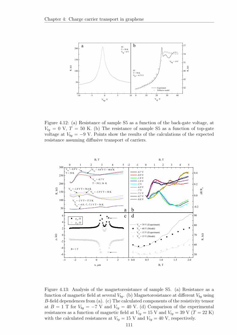
Chapter 4: Charge carrier transport in graphene
0 10 20 30 40
42
45
48
51
54
57
-10 -5 0 5 100
50
100
150
200
R, k
Experiment Diffusive model
Vbg = -9 V
Vtg, V
S5T = 50 KVD = -0.75 V
b
R, k
Vbg, V
S5T = 50 KVtg = 0 V
a
Figure 4.12: (a) Resistance of sample S5 as a function of the back-gate voltage, atVtg = 0 V, T = 50 K. (b) The resistance of sample S5 as a function of top-gatevoltage at Vbg = −9 V. Points show the results of the calculations of the expectedresistance assuming diffusive transport of carriers.
50
100
150
200
250
3000 1 2 3 4 5 -2 -1 0 1 2 3 4 5
-0.2
0.0
0.2
0.4
-3 -2 -1 0 1 2 3
-6
-4
-2
0
2
4
6
0.0 0.5 1.0 1.5 2.0
50
60
70
80
90dca
B, T
Vbg
= -6.9, -7, -7.1 V T = 36 K
Vbg
= -2 V T = 37.5 K
Vbg
= -1.8 V T = 38.6 KV
bg = -1.9 V T = 38 K
Vbg
= -0.9 V T = 39 K
Vbg
= -0.7 V T = 39.5, 36 K
Vbg
= -0.8 V T = 40.6 K
R, k
b
-0.7 V -0.9 V -1.8 V -1.9 V -2 V -6.9 V -7 V -7.1 V -0.7 V -0.8 V
R
/R0
B, T
, k
x, m
xx
,
xy
,
B = 1 T
R, k
Vtg = 39 V (Experiment)
Vtg = 40 V (Model)
Vtg = 15 V (Experiment)
Vtg = 15 V (Model)
B, T
Figure 4.13: Analysis of the magnetoresistance of sample S5. (a) Resistance as afunction of magnetic field at several Vbg. (b) Magnetoresistance at different Vbg usingB-field dependences from (a). (c) The calculated components of the resistivity tensorat B = 1 T for Vbg = −7 V and Vtg = 40 V. (d) Comparison of the experimentalresistances as a function of magnetic field at Vtg = 15 V and Vtg = 39 V (T = 22 K)with the calculated resistances at Vtg = 15 V and Vtg = 40 V, respectively.
111

Chapter 5
Noise in graphene
5.1 Introduction
In this chapter we describe 1/f noise measurements in graphene and few-layer
graphene samples. It is important to investigate the noise properties of graphene
if its properties such as its high mobility at room temperature are to be explored
in electronic applications. A decrease of the noise in the Dirac point of few-layer
graphene in a wide temperature range and a decrease in the noise in the Dirac
point of graphene above 50 K have been observed. We will discuss possible physical
reasons for this behavior.
The first part of this chapter is an introduction to the 1/f noise physics of
conventional MOSFET structures and nanotubes (graphene rolled into a cylinder).
Knowledge of the origin of noise in MOSFETs (based on Si/SiO2) is crucial for un-
derstanding that in graphene on Si/SiO2 substrate. It is also important to compare
the noise in graphene with that in nanotubes due to the strong material similarity.
In the second part, the experimental results on noise are presented and dis-
cussed for multilayer and single-layer graphene. Similarities between nanotubes and
graphene both placed on top of SiO2 can be used to understand the origin of 1/f
noise in graphene.
5.2 Noise in conventional systems
The phenomenon of 1/f noise has been observed in many different electronic sys-
tems. It has been extensively studied in silicon MOSFET structures [6]. Here, the
112

Chapter 5: Noise in graphene
influence of the charge traps in the SiO2 was recognised as the primary source of
the noise [75]. Occupancy of these traps by charge carriers can change the current
in the MOSFET by Coulomb interaction and by fluctuating carrier concentration in
the channel. This leads to temporal switching of the current depending on the occu-
pancy of a trap – Random Telegraph Noise (RTN). The model of many RTN signals
(Sec. 1.3.4) with a broad range of characteristic times is usually used to explain
the appearance of the 1/f spectral power dependence (discussed below). However,
the existence of 1/f noise not only in MOSFET but also in many other electronic
systems suggests that a more fundamental and universal mechanism might exists,
but it has not been discovered yet.
Hooge’s empirical relation [76] provided a useful transformation between the nor-
malised noise amplitude and number of mobile carriers in the system. The relation
comes from the assumption of a Poisson distribution of random fluctuations and is
applied to many studied systems, although it is not universal [10]. This relation
states that the normalised noise power, SR, of resistance fluctuations is inversely
proportional to the number of carriers, N : [76]:
∆SR
R2=
α
N
1
f, (5.1)
where α is a factor which depends on the material and f is the frequency. A smaller
number of carriers N leads to larger relative fluctuations of the resistance R.
5.2.1 1/f noise in MOSFETs
Here we discuss two models for 1/f noise in MOSFETs commonly used in literature.
Impurities in SiO2 play an important part in these models. A sketch of a gated
MOSFET with impurities close to the 2DEG is shown in Fig. 5.1.
Using the Drude formula, Eq. 4.24, which describes the conductivity in metallic-
like two-dimensional samples, conductivity fluctuations can be written as
∆σ = ∆neµ + ne∆µ, (5.2)
where ∆n represents the concentration fluctuations of mobile carriers, and ∆µ the
mobility fluctuations. One of the 1/f noise models in MOSFETs, proposed by
113

Chapter 5: Noise in graphene
Figure 5.1: Model of charge traps at the Si/SiO2 interface. (a) The band diagramwith bias Vg applied to the gate. (b) A zoomed-in region near the interface wheretunnelling between the 2DEG and traps occurs.
Hooge [77], suggests that the mobility fluctuations are the reason for 1/f noise in
inversion layers in MOSFETs. The power spectral density of mobility fluctuations
is given by
Sµ = µ2 αH
Nf, (5.3)
where αH is called Hooge’s constant and equal to ∼ 2 × 10⁻³ for many two-
dimensional systems.
A magnetic field and specific sample geometry (Corbino disk) can be used to
distinguish between fluctuations in concentration and mobility [78]. Basically the
statement is that noise has to disappear at the point where the product of the mo-
bility at zero field and magnetic field is equal to unity, namely mobility fluctuations
are given by [6]
Sµ(f,B)
µ2=
(1− (µ0B)2
1 + (µ0B)2
)2Sµ(f, 0)
µ20
, (5.4)
where µ = µ0/(1 + (µ0B)2) is the mobility in magnetic field, and µ0 is the mobility
at B = 0. This has been tested in n-GaAs systems where it was shown that the
noise power spectral density is independent of magnetic field. Therefore in these
systems the noise originates from fluctuations in the number of carriers, but not in
the mobility [79].
The second model which was, historically, first introduced by McWhorter [11]
describes how 1/f noise originates from fluctuations in the number of mobile carriers.
114

Chapter 5: Noise in graphene
These fluctuations occur naturally when electrons in the 2DEG jump to the traps in
SiO2, Fig. 5.1(b). Scorfield and Fleetwood [75] in a similar model assumed that the
distribution of the traps, which in general is dependent on energy and distance from
the 2DEG, is constant and independent of the coordinate: nt(Et, x) = n0t. Because
the probability of tunnelling is exponentially depend on distance, the autocorrelation
function for this random process is given by [75]
Gnt(∆t) =n0t
LWf(E, T )(1− f(E, T ))e
−|∆t|τ(E) , (5.5)
where τ(E) is the characteristic time for tunnelling, the product LW is the area of
the sample, and f(E, T ) is the Fermi-Dirac distribution. A Fourier transform of the
last expression gives the power spectral density for the corresponding RTN signal,
Snt =n0t
LWf(E, T )(1− f(E, T ))
4τ(E)
1 + (2πfτ(E))2. (5.6)
To get the total noise power one has to integrate over the energy and distance of the
traps from the Si/SiO2 interface. This can be simplified at low temperatures where
the product f(E, T )(1− f(E, T )) can be replaced by the Dirac-delta function. The
total power spectral density of the number of carriers is then given by [75]
SNt ≈kTDt(EF )
LW ln τ1/τ0
1
f, (5.7)
where τ0 and τ1 are the limits related to the cut-offs for low and high frequencies,
Dt(EF ) = x1n0t is the number of traps per unit area and per unit energy at the
Fermi level. It can be seen that the noise in this model has a linear temperature
dependence. The measured relative noise is related to SNt via the capacitance of
the oxide Cox asSV
V 2=
(e
Cox(Vg − VT )
)2
SNt =SNt
n2, (5.8)
where V is a source-drain voltage, Vg is the gate voltage (Fig. 5.1(a)), VT is a
threshold voltage where the conduction of the inversion layer starts.
115

Chapter 5: Noise in graphene
5.2.2 1/f noise in carbon nanotubes
Noise in carbon nanotubes (CNT) has been studied because of its importance in
device applications. By studying the influence of the material of the contacts to a
semiconducting nanotube FET in the ballistic regime, Appenzeller et al. [80] showed
that 1/f noise comes from fluctuation in the number of carriers in the channel
but not fluctuations of the mobility. They found Hooge’s constant to be equal
to 7.5 × 10⁻⁴. In contradiction with this result, a study [81] has shown that the
mobility does fluctuate, and with a much larger Hooge’s constant equal to 9.3×10⁻³.
They have found that the normalised noise does not obey Eq. 5.8, but SV /V 2 ∝1/|Vg − VT | ∝ 1/n. An additional result in this paper was that the adsorbates on
the nanotube do not effect the noise: no difference was found in the noise of the
nanotube in vacuum and exposed to air.
The influence of impurities in the substrate on CNT noise has also been studied
[82]. The authors measured 1/f noise in a nanotube on a Si/SiO2 substrate before
and after removing part of the SiO2 under the nanotube substrate, and found that
noise was reduced by an order of magnitude.
5.2.3 Experiments on 1/f noise in graphene nanoribbons
Previously, 1/f noise has been observed in graphene nanoribbons [20, 83]. The
width of these nanoribbons is so small (about 20 nm) that a bandgap of about
26 meV is formed [20], making them a narrow-gap semiconductors. 1/f noise in
several two-terminal field-effect transistors has been studied at room temperature.
The resistance as a function of back-gate voltage of one single-layer device and one
double-layer sample are shown in Fig. 5.2(a). The resistivity peak is about 32 kOhm
(it is about order of magnitude higher than in our samples) in the Dirac point. The
amplitude of the noise, defined as AN = fSI/I2, changes from 10−6 Hz−1 at high
concentration (±20 V) to 2.5 · 10−6 Hz−1 in the Dirac point. This observed increase
of the noise is similar to the behaviour of 1/f noise in normal MOSFET structures
and carbon nanotubes. The authors claim that Hooge is applicable for graphene
nanoribbons and found αH = 10−3. The experiment with a double-layer graphene
has shown a qualitatively different behaviour of noise amplitude as a function of
gate voltage. The noise amplitude has a dip in the Dirac point, Fig. 5.2(c). The
116

Chapter 5: Noise in graphene
Figure 5.2: (a) Resistance of one single-layer and one bilayer graphene nanoribbondevices measured as a function of gate voltage (at T = 300 K). The two deviceshave identical channel layout (width W = 30 nm and length L = 2.8 µm) as shownin the inset. (b) The resistance, R, and the noise amplitude AN , of the single-layergraphene nanoribbon device measured as a function of gate voltage. The dashedcurve is a guide to the eye, illustrating the correlation between AN and R. (c) Theresistance and the noise amplitude of the bilayer graphene device measured as afunction of gate voltage. The dashed curve is a guide to the eye, illustrating theinverse relation between AN and R. Adapted from [83].
amplitude of the noise in the Dirac point decreased in comparison to the single
layer by 25 times. However it appears that due to small width (∼ 30 nm) of the
nanoribbon the authors are dealing with a regular narrow-gap semiconductor (∼ 20
meV), but not with single-layer graphene with a zero band gap.
5.3 Experiments and analysis
5.3.1 1/f noise in multilayer graphene
Sample ML2 has a thickness of ∼ 2 nm (estimated by eye using the difference in
the visibility contrast of different flakes) which corresponds to about 4 layers of
graphene. The sizes of the sample are given in Table 2.2. The sample cannot be
thicker than 10 layers, because otherwise it would not have good gate control seen
experimentally. We expect that 1/f noise would be too small to be measured in
the case of a bulk graphite sample where all traps in the SiO2 are well screened and
117

Chapter 5: Noise in graphene
log f10
Figure 5.3: Noise in a multilayer graphene sample ML2 after ethanol doping. (a)An example of the spectrum measured up to 100 Hz at 0 V on the gate at T =300 K. The slope of the fit is about 1. (b) The dependence of the resistance noisespectral power at 1 Hz as a function of gate voltage. Inset: the resistances for eachgate voltage where noise has been measured. One can clearly see that the dip in thenoise corresponds to the resistance peak.
cannot change much the concentration or mobility of the sample. This two-terminal
device has been used for noise measurements at room temperature with two different
dopants (ethanol and tap water), and also at 4.2 K in a helium dewar. Spectra have
been taken in the range from 0.25 to 100 Hz at room temperature and from 0.5 Hz
to 400 Hz at liquid helium temperature. For a given resistance, R, the noise power
SV was found to scale with the square of Vsd across the sample as expected. in
addition, we have not observed at room temperature any nonlinear current-source-
drain voltage characteristics. An influence of the doping by tap-water and ethanol
on noise in multilayer graphene (the doping is made by placing a droplet of tap
water or ethanol on top of the sample).
The background noise at Vsd = 0 has been subtracted from the total noise to
get excess noise with 2 mV applied across the sample at room temperature. Then,
the noise power has been divided by the square of voltage to obtain the quantity
SR/R2 = SV /V 2 as a function of frequency. The obtained dependence has been
fitted to check the power dependence for 1/fα noise. The slope α is about 1 ± 0.1
for all measured resistances (an example of noise measured in the Dirac point is
118
Chapter 5: Noise in graphene
shown in Fig. 5.3(a)). From the fit we have obtained the magnitude of the noise at
1 Hz and plotted it in the Fig. 5.3(b), as a function of Vbg.
The position of the Dirac point is shifted to zero voltages after ethanol doping.
The main feature of the noise dependence on back-gate voltage in the sample doped
by ethanol is the observation of the noise minimum at the position of the resistance
peak (see the inset in Fig. 5.3(b)). Such behaviour of noise is in contradictions with
Hooge’s relation which states that the largest resistance fluctuations are observed
at small carrier concentration, Eq. 5.1.
After tap water doping, the Dirac point is shifted to positive gate voltages (the
position of the Dirac point is about 15 V). The slope of the power spectral density
of noise dependence on frequency has a good stability and is always very close to 1,
Fig. 5.4(a). The minimum in the noise is again observed, but it has been shifted so
that the position of the dip corresponds to the new position of the Dirac point. This
is shown in Fig. 5.4(b). This suggests that the minimum in noise is not related to
a specific distribution of impurities in the oxide, but is a result of different physics
in the Dirac point. It is seen that the smallest noise observed in the Dirac point of
sample ML2 at 300 K is ∼ 10−8 Hz−1.
It is known that there are electron-hole puddles in single-layer and double-layer
graphene near the Dirac point [60, 84]. If the noise has a minimum in the Dirac
point which is shifted due to doping, it has to be related to the properties of the
graphene itself, but not to the properties of the SiO2. Below is a qualitative model
how the presence of puddles near the Dirac point can explain the noise dip.
Lets assume that we have a finite concentration of the two types of carrier (N(t)
is for electrons and P (t) is for holes) in the puddles. Let us also assume that we can
write the noise in terms of the fluctuations of the number of carriers as
SV
V 2=
(∆N
N+
∆P
P
)2
, (5.9)
where ∆N is a random fluctuation in number of electrons.
Eq. 5.9 can be simplified if we take into account that for random fluctuations
∆N/N = 1/√
N and ∆P/P = 1/√
P , and that the average number of carries in the
electron and hole puddles changes with gate voltage as N0 +CVg/2 and N0− cVg/2,
respectively. Assuming that the number of electrons and holes in the puddles is the
119

Chapter 5: Noise in graphene
Figure 5.4: Noise in sample ML2 after tap-water doping. (a) An example of thespectrum measured up to 100 Hz at 0 V on the back-gate at T = 300 K. The slopeof the fit is about 1. (b) The dependence of the resistance noise at 1 Hz as a functionof back-gate voltage. Inset: the resistances for each back-gate voltage where noisehas been measured.
-40 -20 0 20 400.0
1.0x10⁻⁸
2.0x10⁻⁸
3.0x10⁻⁸
4.0x10⁻⁸
5.0x10⁻⁸
10 100
10-11
10-10
10-9
-40 -20 0 20 400
5
10
15
20
25
SR/R
2 (
at
1 H
z),
Hz
-1
ML2
T = 4.2 K
Vbg
, V
ba
Isd
25 nA
50 nA
100 nA
Fit
ML2
T = 4.2 K
Vbg
= -30 V
log10
(SR/R
2) = -8.2 - 1.012 log
10f
SR/R
2,
Hz
-1
f, Hz
R,
kΩ
Vbg
, V
Figure 5.5: Noise in sample ML2 at 4.2 K. (a) An example of the spectrum at -30 V on the back-gate at T = 4.2 K for three source-drain currents calculated asSV /(RIsd)
2. The slope of the fit is about 1. (b) The dependence of the resistancenoise at 1 Hz as a function of back-gate voltage. Inset: the resistances for eachback-gate voltage where noise has been measured.
120

Chapter 5: Noise in graphene
same at zero gate voltage:
SV
V 2=
1√
N + CVg
2
+1√
N − CVg
2
2
αM
f
=
2N
N2 − (CVg)2
4
+2√
|N2 − (CVg)2
4|
αM
f. (5.10)
where αM is a constant which, in general, can depend on temperature and magnetic
field.
This expression leads to a minimum in the noise in the Dirac point where Vg = 0
and the maximum near the region where the total number (both electrons and holes)
of carriers in the puddles is equal to the number of carriers produced by the gate.
Here, we can interpret Eq. 5.10 as a modified Hooge’s relation for graphene. If
we consider a hole Vg-region with the total number of carriers P1(t) in the puddle,
it will fluctuate as a normal sample with one type of carrier, SV /V 2 ∝ 1/P1: i.
e. each uniform part of the graphene sample obeys the Hooge relation. When
we apply a small gate voltage we change the concentration in the puddle: if we
decrease number of holes relative fluctuations will increase and if we apply negative
gate voltage the noise decreases in this puddle according to the Hooge relation.
When the gate voltage is large enough, CVg À N0, to produce a sample without
puddles we have to have a standard metallic system which obeys the Hooge relation,
SV /V 2 ∝ 1/(CVg).
Because the number of carriers in the puddles has to be dependent on the tem-
perature the existence of temperature dependence naturally appears in the model:
namely the noise in the Dirac point at room temperature has to be smaller than at
lower temperature (if we forget for a moment about temperature dependence of the
noise amplitude, αM).
The temperature was decreased to 4.2 K to see the effect on the noise power.
The result is shown in Fig. 5.5(a). The dip in the noise is still seen at the Dirac
point. However, the power density of the noise has dropped to a smaller value in
the Dirac point. The decrease is about 6 times in the hole region, and 20 times in
the Dirac point. It is clearly seen that the electron region has larger noise than the
hole region and the ratio between the noise in the Dirac point and the noise power
121

Chapter 5: Noise in graphene
Figure 5.6: Resistance noise at T=0.26 K for sample SL4. (a-c) Spectra for differentback-gate voltages -7.5 V, -1.5 V, and -3 V. (RTN is better seen in (c).) Red solidlines are the best fit using equation 5.11. (d) Solid circles show resistance powerspectral density for extrapolated values at 1 Hz. The empty circles represent 1/fnoise power at 1 Hz without the contribution of RTN, arrows show the change in1/f noise amplitude when RTN is taken into account. Triangles show the resistanceas a function of back-gate voltage.
at 45 V on the back-gate is 0.01 (see Fig. 5.5(b)).
Voss [85] has discussed how gate voltage fluctuations can affect 1/f noise. As-
suming that these fluctuations can originate from the non-stable voltage source, or
fluctuating occupancies of impurities in SiO2 can produce effective fluctuating Vg,
we can conclude that relative resistance fluctuations ∆R/R are proportional to the
derivative of the resistance with respect to gate voltage dR/dVg. In this case the
noise would have a minimum in the Dirac point (where dR/dVg = 0 ) and two max-
ima where the second derivative is zero (thus the first derivative has a maximum).
A leakage current between the gate and the sample occurs through defects in the
SiO2 and causes fluctuations in voltage across the sample. In this case the noise
will be proportional to the resistance of the sample. However, in our experiments
we have tested the leak between the gate and the sample and the expected position
of the maxima have not been observed.
122

Chapter 5: Noise in graphene
Figure 5.7: Noise measured in sample SL4 by lock-in amplifier at T = 24 K with 1µA constant source-drain current as a function of back-gate voltage. Forward andbackward sweeps are presented by different colors. Resistance as a function of back-gate voltage is shown at 24 K (solid line) and several resistances at base temperaturefrom Fig. 5.6 are presented by open circles. The two lowest curves (backgrounds)are measured without applied voltage across the sample.
5.3.2 1/f noise in single-layer graphene
Resistance noise has also been measured in sample SL4 at base temperature of
Helium-3 system (0.26 K). The slope of the spectra for several points in back-gate
voltage near the Dirac point deviates from 1, Fig. 5.6. We have attributed this
to a strong effect of a single impurity which can modulate the resistance of the
sample and produce (RTN) resistance noise which is added to 1/f noise. The total
resistance noise, StotR , is then described by the equation
StotR
R2=
SRTNR
1 + (2πfτ)2+
S1/fR
f, (5.11)
where SRTNR and S
1/fR are power spectral density for RTN and 1/f noise, respectively,
and τ is a characteristic time of the RTN. The quality of the fit is shown in Fig.
5.6(a-c) by the red curves. If the contribution to the total noise from the RTN is
removed, the resulting 1/f noise is found to be independent of the back-gate voltage
from -10 V to 5 V, Fig. 5.6(d). This is different from the noise behaviour in sample
ML2, where a dip in the noise is observed in the Dirac point at low temperature.
For sample SL4, we have tested the influence of the current contacts on noise.
123

Chapter 5: Noise in graphene
If the voltage noise in the contacts produces fluctuations in the current, this will
be seen as voltage noise on the sample. However, this (normalised) noise will be
reduced by a factor (rRc/R2b)
2, where r is the sample resistance, Rc is the contact
resistance, and Rb is a large ballast resistance. In this test we have taken r = 2.85
kΩ (at Vbg = 0 V and T = 8.5 K) and two ballast resistors of 10 MΩ and 100 MΩ.
The 1/f noise showed no difference between these two ballast resistors up to 0.25
mV applied (the noise was 1.2 · 10−8 Hz−1). Therefore this coefficient of suppression
(∼ 10−8) is large enough to neglect the contribution of the current contacts to the
total noise.
The sample has a weak temperature dependence of the resistance, if one compares
the resistance at T = 24 K (solid line) and at T = 0.26 K (empty circles), Fig. 5.7.
At T = 24 K we have measured the integral noise in sample SL4 by lock-in amplifier
at 1 µA source-drain current, Fig. 5.7. The lock-in amplifier has been used to
integrate the spectral amplitude of the signal in the bandwidth, 1/8τ , around a
central reference frequency, f0 = 1 kHz. The result is shown in Fig. 5.7 by black
and red noisy curves. The background (flatline in Fig. 5.7) is constant and comes
from the noise of the preamplifiers. Nonmonotonic excess noise appears when a
source-drain current is applied. This has a maximum not only in the Dirac point,
where noise has to be larger due to the larger voltage applied, but also maxima in
the region close to the Dirac point. The strongest peaks occurs at Vbg = −1 V and
at 5 V from the Dirac point. The width of the peak at Vbg = −1 V is about 150 K
(here we have used the expression for the change in the Fermi energy due to change
of back-gate voltage ∆εF = 30 [meV] ∆V [V]/2√
V [V]), which is much larger than
the temperature. We attribute this peak to the existence of impurities in the SiO2 or
on top of the flake in this sample. These impurities have a contribution to the noise
amplitude only in a narrow back-gate voltage span of about 2 V, when the Fermi
energy crosses the energy band (maxima in the density of states) occupied by the
impurities. It is interesting to note that the low temperature measurements, Fig.
5.6 have shown 1/f noise with a slightly steeper slope, −1.31 instead −1 (for 1/f
noise) at Vbg = −1.5 V, for another point at Vbg = 0 V there is no RTN contribution
to the noise. It is worth mentioning that the half width of the noise peak is smaller
than the distance between the peak and Vbg = −3 V where a clear RTN spectrum
is observed, Fig. 5.6(c). We can conclude that the RTN observed at Vbg = −1 V is
124

Chapter 5: Noise in graphene
-60 -40 -20 0 200.0
2.0x10⁻⁸
4.0x10⁻⁸
6.0x10⁻⁸
8.0x10⁻⁸
0
1
2
3
1 10 100
10-10
10-9
10-8 StotR
S1/fR
S R/R
2 (at 1
Hz)
, Hz-1
Vbg
, V
SL4T = 8.75 K
ba
R, k
R
SL4T = 8.75 KVbg = -12 V
S R/R
2 , Hz-1
SRTN2R = 7.42 · 10-9 Hz-1
= 0.055 s
S1/fR = 5.92 · 10-9 Hz-1
SRTN1R = 7.72 · 10-11 Hz-1
= 0.00065 s
Experiment Fit 1/f RTN1 RTN2
f, Hz
Figure 5.8: (a) Power spectral density at 1 Hz as a function of back-gate voltage atT = 8.75 K for sample SL4. (b) Fitting the spectrum at Vbg = −12 V using twoRTN signals and 1/f spectrum.
not related to the RTN at Vbg = −3 V. It is also seen that the strong RTN signal at
Vbg = −3 V is not present in the integrated noise dependence on back-gate voltage.
To see how temperature affects the noise, 1/f noise as a function of Vbg at 8.75
K has been measured in sample SL4. Figure 5.8(a) shows a dip in noise at 0 V
(black squares). The amplitude of the noise increases from 0.5 × 10⁻⁸ Hz−1 (Dirac
point) to 6× 10⁻⁸ Hz−1 (at −40 V), and the noise decreases at higher gate voltages.
Even less scattered data can be obtained if we take into account the contribution of
several RTNs in the total spectrum as it shown in Fig. 5.8(b), where two RTNs with
amplitudes 7.72× 10⁻¹¹ Hz−1 and 7.42 · 10−9 Hz−1 are detected. The resulting noise
dependence on gate voltage (empty circles) has more monotonic behaviour. This
behaviour is in qualitative agreement with Eq. 5.10: there is a deep in the Dirac
point, and a maximum in the noise is seen at Vbg = −40 V, and the noise decreases
at larger negative voltages.
125

Chapter 5: Noise in graphene
10 100
10-10
10-9
10 100
10-11
10-10
10-9
10-11
10-10
10-9
10-81 10 100
10 10010-10
10-9
Isd
100 nA 200 nA 400 nA Fit
SR/R
2 , Hz-1
f, Hz
SL4Vbg = 0 VR = 3.4 kT KB = 2 T
log10SV /V2 =-8.05-1.00 log10f
Isd SR/R
2 , Hz-1
50 nA 100 nA 200 nA Fit
log10SV /V2 =-8.39-0.90 log10f
f, Hz
SL4Vbg = -6 VR = 3.5 kT KB = 0 T
dc
ba
Isd
100 nA 200 nA 400 nA Fit
f, Hz
log10SV /V2 =-8.09-1.00 log10f
S R/R
2 , Hz-1
SL4Vbg = 0 VR = 2.39 kT KB = 0 T
Isd
50 nA100 nA200 nA Fit
SR/R
2 , Hz-1
f, Hz
SL4Vbg = -6 VR = 4.5 kT KB = 2 T
SRTN
R 1.21 10-9 Hz-1
S1/fR 1.64 10-8 Hz-1
0.00281 s0.84
Figure 5.9: Spectra for sample SL4 at 8.75 K at three source-drain currents. (a-b)1/f noise spectra away from the Dirac point show good 1/f dependence withoutmagnetic field (a) and with B = 2 T applied (b). (c-d) Noise at the Dirac point.
5.3.3 Influence of magnetic field on 1/f noise
We have tested the influence of magnetic field on 1/f noise in single-layer graphene
at T = 8.75 K. For sample SL4 two points in the back-gate voltage have been
taken: 0 V and −6 V (Dirac point). We have measured noise spectra at magnetic
fields of 0 T and 2 T applied perpendicular to the sample, Fig. 5.9. At back-gate
voltage equal to 0 V (which is away from the Dirac point) we have observed a good
1/f frequency dependence of the spectra, with a small change in noise amplitude
between 8.1 × 10⁻⁹ Hz−1 at 0 T and 8.9 × 10⁻⁹ Hz−1 at 2 T. The resistance also
changes from 2.39 kOhm as 0 T to 3.4 kOhm at 2 T. In the Dirac point 1/fα noise
has been observed without magnetic field, where α = 0.9. When a magnetic field of
2 T was applied a RTN appeared and the amplitude of noise SR/R2 increased from
4.07 × 10⁻⁹ Hz−1 to 1.64 × 10⁻⁸ Hz−1. Thus there is a transition in magnetic field
from the situation when noise in the Dirac point is the smallest to the case where
it is the largest. We have not studied this effect in detail, and we do not have yet
126
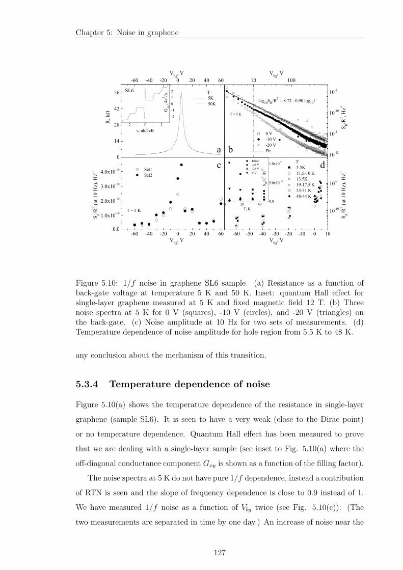
Chapter 5: Noise in graphene
-60 -50 -40 -30 -20 -10 0 10
10-10
10-9
-60 -40 -20 0 20 40 600.0
1.0x10⁻¹⁰
2.0x10⁻¹⁰
3.0x10⁻¹⁰
4.0x10⁻¹⁰
0
14
28
42
56
-60 -40 -20 0 20 40 60 10 100
10-12
10-11
10-10
10-9
-2 0 2
-2
-10
1
2
0 20 400.0
5.0x10⁻¹⁰
1.0x10⁻⁹
T 5.5K 11.5-10 K 13.5K 19-17.5 K 33-31 K 48-44 K
Gxy
, 4e2 /h
Vbg, VVbg, V
Vbg, VVbg, V
R, k
S R/R
2 , Hz-1
S R/R
2 (at 1
0 H
z), H
z-1
Set1 Set2
S R/R
2 (at 1
0 H
z), H
z-1
T = 5 K
dca b
SL6
, nh/4eB
T 5K 50K
T = 5 K
log10SR/R2 =-8.72 - 0.90 log10f
0 V -10 V -20 V Fit
SR
/R2 ,H
z-1
T, K
Dirac -40 V -20 V 0 V
Figure 5.10: 1/f noise in graphene SL6 sample. (a) Resistance as a function ofback-gate voltage at temperature 5 K and 50 K. Inset: quantum Hall effect forsingle-layer graphene measured at 5 K and fixed magnetic field 12 T. (b) Threenoise spectra at 5 K for 0 V (squares), -10 V (circles), and -20 V (triangles) onthe back-gate. (c) Noise amplitude at 10 Hz for two sets of measurements. (d)Temperature dependence of noise amplitude for hole region from 5.5 K to 48 K.
any conclusion about the mechanism of this transition.
5.3.4 Temperature dependence of noise
Figure 5.10(a) shows the temperature dependence of the resistance in single-layer
graphene (sample SL6). It is seen to have a very weak (close to the Dirac point)
or no temperature dependence. Quantum Hall effect has been measured to prove
that we are dealing with a single-layer sample (see inset to Fig. 5.10(a) where the
off-diagonal conductance component Gxy is shown as a function of the filling factor).
The noise spectra at 5 K do not have pure 1/f dependence, instead a contribution
of RTN is seen and the slope of frequency dependence is close to 0.9 instead of 1.
We have measured 1/f noise as a function of Vbg twice (see Fig. 5.10(c)). (The
two measurements are separated in time by one day.) An increase of noise near the
127
Chapter 5: Noise in graphene
Dirac point is seen for both sets of measurements. The noise increased by an order
of magnitude from a high-conduction hole region to the Dirac point. This is usual
behaviour for standard MOSFET structures (except for the last point at 60 V).
In Fig. 5.10(d) the temperature dependence of noise is shown from 5 K (filled
squares) to 48 K (filled triangles) where one can see an increase of noise with in-
creasing temperature at high hole concentration (Vbg = −60 V, −40 V, −20 V) by
factor of 2. However, close to the Dirac point (−4.7 V) the noise amplitude shows
an opposite behaviour: the noise decreases with increasing temperature. It is clearly
seen in the inset to Fig. 5.10(d) where the results for four gate voltages are presented
as a function of temperature. This unusual effect has not been observed before. It
highlights the difference in the origin of noise in the Dirac point and may be related
to the presence of the minimum in the dirac point in sample SL4.
The influence of the temperature on noise in sample SL6 has been studied in
another cool-down. The noise dependence on gate voltage has been measured for
three temperatures (140 K, 100 K, and 60 K). The results of measurements for the
highest temperature are presented in Fig. 5.11. The difference of the resistance in
the Dirac point at T = 140 K and T = 50 K is less than 10 %. At T = 140 K noise
amplitude as a function of back-gate shows a dip in the Dirac point. In addition,
two maxima in noise amplitude have been observed: at Vbg = 1 V and Vbg = 5.5
V. These maxima do not correspond to the maxima in the squared derivative of
the sample resistance with respect to Vbg and cannot therefore be related to same
effective gate voltage fluctuations.
It has been shown that the noise decreases from 140 K to 60 K, Fig. 5.12(a).
The decrease is larger at higher gate voltage (by order of magnitude at Vbg = −20
V) but in the Dirac point the noise amplitude is smaller only by 3 times. The dip
in the noise amplitude as a function of Vbg seen at 140 K and 100 K is absent at
T = 60 K. This interesting observation requires more detailed studies.
128

Chapter 5: Noise in graphene
0
10
20
30
40
50
-20 -10 0 10 20
-20 -15 -10 -5 0 5 10 15 203.0x10⁻⁹
6.0x10⁻⁹
9.0x10⁻⁹
0
50
100
150b
Vbg, V
R, k
a
2.5 V
S R/R
2 (at 1
Hz)
, Hz-1
Vbg, V
4.5 V
(dR
/dV
bg)2 , k
2 V-2
SL6T= 140 K
Figure 5.11: 1/f noise in graphene SL6 sample at T = 140 K. (a) Resistance as afunction of back-gate voltage at T = 140 K. Points show the resistances for eachback-gate voltage where noise has been measured. (b) The resistance noise at 1 Hzas a function of Vbg (left ordinate axis), and the squared derivative of the sampleresistance with respect to Vbg as a function of Vbg (right ordinate axis).
-20 0 20
10-9
10-8
1 10
10-9
10-8
b
140 K 100 K 60 K
S R/R
2 (at 1
Hz)
, Hz-1
Vbg, V
a
140 K100 K60 K
SR
/R2 (a
t 1 H
z), H
z-1
Vbg -VD, V
Figure 5.12: 1/f noise in graphene SL6 sample at three temperatures. (a) Theresistance noise at 1 Hz as a function of Vbg at 140 K (squares), 100 K (circles), and60 K (triangles) temperatures. (b) The dependence of the resistance noise (electronregion) at 1 Hz on (Vbg − VD) in log-log scale. The solid lines have slopes equal to-0.5.
129

Chapter 5: Noise in graphene
Fig. 5.12(b) shows the dependence of the resistance noise (electron region) at 1
Hz as a function of (Vbg−VD), where VD = 3.3 V, in log-log scale. The lines have the
slope equal to −0.5. Good agreement is seen with a square root dependence of the
noise amplitude on (Vsd− VD). This gives another interesting feature of single-layer
graphene: the Hooge relation is not applicable for graphene because in experiment
SR/R2 ∝ (Vbg − VD)−1/2f−1 ∝ N−1/2f−1. (5.12)
Such behaviour of 1/f noise is observed in a wide range of temperatures, from 5 K
to 140 K.
5.3.5 Current-voltage characteristic
If the differential resistance changes as a function of source-drain bias it will affect
the measured noise. Therefore the nonlinearity in the current-voltage characteristic
has to be taken into account. The measured monolayer (SL4 and SL6) and multilayer
(ML2) graphene samples have shown a linear I(Vsd) at room temperature: SL4 and
SL6 in the studied range of Vsd up to 1 mV, and ML2 up to 10 mV. A nonlinearity
can occur at lower temperature.
A question about the influence of the contacts on the voltage dependence of the
differential resistance appears due to possible the Shottky barrier between graphene
and a metallic contact. In Fig. 5.13 we show the results of the normalised differential
resistance dependence on DC current for sample SL6 at T = 5.5 K using two- and
four-terminal measurements (where contacts are not important) where one can see
that there is no significant difference between two types of connections. We conclude
from this that all nonlinearity comes from the properties of the graphene itself.
5.3.6 Shot noise in graphene sample SL6
Shot noise has been measured in two back-gate voltages of -60 V and -40 V. The
resistances at these voltages are 2.28 kΩ and 2.48 kΩ at base temperature (0.26
K). The spectra have been measured at four different source-drain currents up to
1000 nA, which produces source-drain voltages up to 2.5 mV across the sample.
A six-terminal device has allowed us to use the cross correlation technique in the
130
Chapter 5: Noise in graphene
frequency range from 50 kHz to 100 kHz where 1/f noise can be neglected. The
results are shown in Fig. 5.14. As one can see the spectra have a slight bending at
high frequencies (5.14(a-b)), caused by parasitic capacitance in the circuit, which is
taken into account by a correction procedure where the measured spectrum, SI is
multiplied by a factor
SSNI = SI(1 + (2πfRC)2), (5.13)
where R is the sample resistance, C is the capacitance of the twisted pairs used
in the circuit, and f is the frequency. It is known that thermal noise has a flat
spectrum. Thus one can determine the capacitance, C, of the wires by “unbending”
the background thermal noise. The determined capacitance is 1250 pF which is in
agreement with the estimated length of the wires.
Once the capacitance of the wires is known, shot noise spectra are obtained
using Eq. 5.13. The average values of each spectra are shown in Fig. 5.14(c-d) by
solid squares. It is seen that the dependence of the current noise on source-drain
current is approximately linear. To compare the current noise with the theoretical
shot noise SI = 2eIF , where F is the Fano factor, red circles are shown for Fano
factors 0.34 and 0.17 for −40 and −60 Volts, respectively. The Fano factor of 0.34
is in agreement with noise measurements in disordered short graphene samples [86]
and the theory for a square sample [87]. The decrease (in disagreement with the
theory [86]) of the Fano factor at higher voltages has not been observed previously.
5.4 Conclusions
It has been shown that the noise in multilayer graphene samples shows a dip in noise
amplitude as a function of back-gate voltage, which can be shifted to a new position
by doping as it follows the Dirac point position.
For a single layer graphene we have found two opposite types of behaviour: a
dip in the Dirac point in one sample (observed in sample SL4 at 8.75 K), but a
noise peak in the Dirac point in another (SL6) at 5 K. However, a dip in noise
amplitude at the Dirac point has been observed in sample SL6 at 100 and 140 K.
More samples for statistics are required to explain this unusual effect. In sample SL6
we have observed an increase of the noise as a function of temperature at high hole
131

Chapter 5: Noise in graphene
concentration, but in the Dirac point noise decreases as a function of temperature
(from 5 K to 50 K), which unveil the presence of different mechanism of noise in
these regions. This effect also requires further investigation.
132

Chapter 5: Noise in graphene
-200 0 200
0.96
0.98
1.00
-200 0 200
0.96
0.98
1.00
a
R (k )
R/R
0
SL6T = 5.5 K2 terminal
I, nA
R/R
0 55.7 49.1 38.3 30.2 24.1 20.1
b
R (k ) 57.6 51 39 31.8 26.2 22.1
I, nA
SL6T = 5.5 K4 terminal
Figure 5.13: Normalised resistance in the Dirac point as a function of source-draincurrent for sample SL6 at 5.5 K. (a) 2 terminal circuit. (b) 4 terminal circuit.
0 250 500 750 10000.0
4.0x10⁻²⁶
8.0x10⁻²⁶
0 250 500 750 10000.0
2.0x10⁻²⁶
4.0x10⁻²⁶
6.0x10⁻²⁶
6x10-19
7x10-19
8x10-19
9x10-19
10-18
50 60 70 80 90 100 50 60 70 80 90 100
6x10-19
7x10-19
8x10-19
9x10-19
dcb
Isd, nA
S I, A2 /H
z
Noise F = 0.34
T = 0.26 KVbg = - 40 V
SI, A
2 /Hz
Isd, nA
Noise F = 0.17
T = 0.26 KVbg = - 60 V
f, kHz
T = 0.26 KVbg = - 40 V
S V/V
2 , 1/H
z
Isd
0 nA 250 nA 500 nA 750 nA 1000 nAa
T = 0.26 KVbg = - 60 V
S V/V
2 , 1/H
z
f, kHz
Isd
0 nA 250 nA 500 nA 750 nA 1000 nA
Figure 5.14: Shot noise in graphene at T=0.26 K. (a) Spectra for different source-drain currents for 50 a kHz span at −40 V on back-gate voltage. (b) Spectra fordifferent source-drain currents for 50 a kHz span at −60 V on back-gate voltage. (c)Current noise (solid squares) as a function of current at Vbg = −40 V. Red circlesshow current noise at Fano factor equal 0.34. (d) Current noise as a function ofcurrent at Vbg = −60 V. Red circles show current noise at Fano factor equal 0.17.
133

Chapter 6
Conclusions and suggestions for
further work
In this thesis the results of experimental studies of transport through double impu-
rities placed in double-barrier resonant tunnelling diode, the ballistic transport of
chiral particles through p-n junctions, and 1/f noise properties of graphene have
been presented. It has been demonstrated that diffusive models can be applied to
the diffusive graphene systems to explain the resistance dependence on back and top
gate voltages. Also the magnetoresistance of a nonuniform sample can be explained
by a geometrical magnetoresistance. It was shown that 1/f noise in graphene has
much more complicated concentration and temperature dependence than that in
usual metals.
We have used magnetic field parallel to the current to investigate resonant tun-
nelling through a double impurity in a vertical double-barrier resonant tunnelling
diode, by measuring current-voltage and differential conductance-voltage character-
istics. Information was obtained about the properties of the impurities: the energy
levels, the effective electron mass and their spatial positions.
The chiral nature of the carriers in graphene has been demonstrated by com-
paring measurements of the transport through a ballistic p-n junction with the
predictions of the diffusive models. This allowed us to find, unambiguously, the
contribution of ballistic resistance to the total resistance of a p-n-p structure.
The first observation of 1/f noise in graphene has revealed a new feature not
observed in conventional metals or semiconductors. The dip in the normalised noise
134

Chapter 6: Conclusions and suggestions for further work
seen in the Dirac point of single-layer graphene at temperatures above 100 K still
requires an explanation. A simple model of two different types of carrier in the Dirac
point seems to be useful to explain the dip in the normalised noise.
Below are some suggestions for further work:
• We have not studied in detail the mutual arrangement of the impurities in the
barriers of a DBRTD, but this can be done by rotation of magnetic field with
respect to the current, in order to reveal the overlap between the wavefunctions
of the two states.
• The studied graphene samples with p-n-p structures did not have large enough
mean free path (or small enough n-region) to make the whole p-n-p structure
fully ballistic. Making such structure would allow one to observe unambigu-
ously the Klein paradox in graphene.
• We have not identified whether fluctuations in concentration or mobility are
the main source of 1/f noise in graphene. This can be done using a Corbino
disc geometry and measure the noise as a function of magnetic field to clarify
this question.
135

Bibliography
[1] J. H. Devies. The Physics of Low-Dimentional Semiconductors: an Introduc-
tion. Cambridge University Press, Cambridge, (1998).
[2] B. M. Askerov. Electron Transport Phenomena in Semiconductors. World
Scientific, Singapore, (1994).
[3] S. Datta. Electronic Transport in Mesoscopic Systems. Cambridge University
Press, Cambridge, (1995).
[4] M. V. Entin. private communication .
[5] A. van der Ziel. Noise in solid state devices and circuits. Wiley-Interscience,
(1986).
[6] Sh. Kogan. Electronic noise and fluctuatiions in solids. Cambridge University
Press, Cambridge, (1996).
[7] R. F. Voss and J. Clarke. Phys. Rev. Lett. 40, 913 (1976).
[8] R. F. Voss and J. Clarke. Phys. Rev. B 13, 556 (1976).
[9] H. Wong. Microelectronics Reliability 43, 585 (2003).
[10] M. B. Weissman. Rev. Mod. Phys. 60, 537 (1988).
[11] A. L. Mc Whorter. Semiconductor surface physics. University of Pennsylvania
press, Philadelphia.
[12] F. N. Hooge, T. G. M. Kleinpenning, and L. K. J. Vandamme. Rept. Progr.
Phys. 44, 479 (1981).
[13] P. Dutta and P. M. Horn. Rev. Mod. Phys. 53, 497 (1981).
136
BIBLIOGRAPHY
[14] C. W. J. Beenakker M. J. M. de Jong. cond-mat/9611140 .
[15] Ya. M. Blanter and M. Buttiker. Phys. Rep. 336, 1 (2000).
[16] S. S. Safonov, A. K. Savchenko, D. A. Bagrets, O. N. Jouravlev, Y. V. Nazarov,
E. H. Linfield, and D. A. Ritchie. Phys. Rev. Lett. 91, 136801 (2003).
[17] J. P. Holder. Thesis: Resonant tunnelling spectroscopy of vertical
GaAS/AlGaAs structures. University of Exeter, (1999).
[18] K. S. Novoselov, D. Jiang, F. Schedin, T. J. Booth, V. V. Khotkevich, S. V.
Morozov, and A. K. Geim. PNAS 102, 10451 (2005).
[19] M. Ezawa. Phys. Rev. B 73, 2006 (045432).
[20] Z. Chen, Y.-M. Lin, M. J. Rooks, and P. Avouris. Physica E 40, 228 (2007).
[21] K. S. Novoselov, A. K. Geim, S. V. Morozov, D. Jiang, M. I. Katsnelson, I. V.
Grigorieva, S. V. Dubonos, and A. A. Firsov. Nature 438, 197 (2005).
[22] Y. Zhang, Y.-W. Tan, H. L. Stormer, and P. Kim. Nature 438, 201 (2005).
[23] V. P. Gusynin and S. G. Sharapov. Phys. Rev. Lett. 95, 146801 (2005).
[24] F. V. Tikhonenko, D. W. Horsell, R. V. Gorbachev, and A. K. Savchenko. Phys.
Rev. Lett. 100, 056802 (2008).
[25] W. R. Frensley. Rev. Mod. Phys 62, 745 (1990).
[26] R. Tsu and L. Esaki. Appl. Phys. Lett. 22, 562 (1973).
[27] M. W. Dellow, P. H. Beton, C. J. G. M. Langerak, T. J. Foster, P. C. Main,
M. Henini, S. P. Beaumont, and C. D. W. Wilkinson. Phys. Rev. Lett. 68, 1754
(1992).
[28] S. J. Bending and M. R. Beasley. Phys. Rev. Lett. 55, 324 (1985).
[29] A. B. Fowler, G. L. Timp, J. J. Wainer, and R. A. Webb. Phys. Rev. Lett. 57,
138 (1986).
[30] T. E. Kopley, P. L. McEuen, and R. G. Wheeler. Phys. Rev. Lett. 61, 1654
(1988).
137

BIBLIOGRAPHY
[31] J. P. Holder, A. K. Savchenko, V. I. Fal’ko, B. Jouault, G. Faini, F. Laruelle,
and E. Bedel. Phys. Rev. Lett. 84, 1563 (2000).
[32] H. C. Liu and G. C. Aers. J. Appl. Phys. 65, 4908 (1989).
[33] P. C. Main, A. S. G. Thornton, R. J. A. Hill, S. T. Stoddart, T. Ihn, L. Eaves,
K. A. Benedict, and M. Henini. Phys. Rev. Lett. 84, 729 (2000).
[34] A. I. Larkin and K. A. Matveev. Sov. Phys. JETP 66, 580 (1987).
[35] A. K. Savchenko, V. V. Kuznetsov, A. Woolfe, D. R. Mace, M. Pepper, D. A.
Ritchie, and G. A. C. Jones. Phys. Rev. B 52, 17021 (1995).
[36] E. Lind, B. Gustafson, I. Pietzonka, and L.-E. Wernersson. Phys. Rev. B 68,
033312 (2003).
[37] T. Schmidt, R. J. Haug, K. v. Klitzing, A. F¨rster, and H. Luth. Phys. Rev.
Lett. 78, 1544 (1997).
[38] V. Fock. Z. Phys. 47, 446 (1928).
[39] I. E. Itskevich, T. Ihn, A. Thornton, M. Henini, T. J. Foster, P. Moriarty,
A. Nogaret, P. H. Beton, L. Eaves, and P. C. Main. Phys. Rev. B 54, 16401
(1996).
[40] T. Schmidt, R. J. Haug, Vladimir I. Fal’ko, K. v. Klitzing, A. F¨rster, and
H. Luth. Phys. Rev. Lett. 78, 1540 (1997).
[41] G. Faini, C. Vieu, F. Laruelle, P. Krauz, E. Bedel, and C. Fontaine. Surface
Science 361.
[42] M. W. Dellow, P. H. Beton, C. J. G. Langerak, T. J. Foster, P. C. Main,
L. Eaves, M. Henini, S. P. Beamont, and C. D. W. Wilkinson. Phys. Rev. Lett.
68, 1754 (1991).
[43] V. V. Cheianov and V. I. Fal’ko. Phys. Rev. B 74, 041403R (2006).
[44] K. S. Novoselov, A. K. Geim, S. V. Morozov, Y. Zhang D. Jiang, S. V. Dubonos,
I. V. Grigorieva, and A. A. Firsov. Science 306, 666 (2004).
[45] P. R. Wallace. Phys. Rev. 71, 622 (1947).
138
BIBLIOGRAPHY
[46] M. I. Katsnelson, K. S. Novoselov, and A. K. Geim. Nature Physics 2, 620
(2006).
[47] M. I. Katsnelson. Eur. Phys. J. B 51, 157 (2006).
[48] D. S. L. Abergel, A. Russell, , and Vladimir I. Fal’ko. Appl. Phys. Lett. 91,
063125 (2007).
[49] P. Blake, E. W. Hill, A. H. Castro Neto, K. S. Novoselov, D. Jiang, T. J. Booth
R. Yang, and A. K. Geim. Appl. Phys. Lett. 91, 063124 (2007).
[50] A. C. Ferrari, J. C. Meyer, V. Scardaci, C. Casiraghi, M. Lazzeri, F. Mauri,
S. Piscanec, D. Jiang, K. S. Novoselov, S. Roth, and A. K. Geim. Phys. Rev.
Lett. 97, 187401 (2006).
[51] N. M. R. Peres, F. Guinea, , and A. H. Castro Neto. Phys. Rev. B 73, 125411
(2006).
[52] V. P. Gusynin, S. G. Sharapov, and J. P. Carbotte. Int. J. Mod. Phys. B 21,
4611 (2007).
[53] A. H. Castro Neto, F. Guinea, N. M. R. Peres, K. S. Novoselov, and A. K.
Geim. Rev. Mod. Phys. .
[54] Gordon W. Semenoff. Phys. Rev. Lett. 53, 2449 (1984).
[55] T. Ando. J. Phys. Soc. Jpn. 74, 777 (2005).
[56] A. K. Geim and K. S. Novoselov. Nature Mater. 6, 183 (2007).
[57] J. H. Chen, C. Jang, M. S. Fuhrer, E. D. Williams, and M. Ishigami. cond-
mat/0708.2408 .
[58] S. V. Morozov, K. S. Novoselov, M. I. Katsnelson, F. Schedin, D. C. Elias, J. A.
Jaszczak, and A. K. Geim. Phys. Rev. Lett. 100, 016602 (2008).
[59] K. I. Bolotin, K. J. Sikes, Z. Jiang, M. Klima, G. Fudenberg, J. Hone, P. Kim,
and H. L. Stormer. Solid State Communications 146, 351 (2008).
[60] J. Martin, N. Akerman, G. Ulbricht, T. Lohmann, J. H. Smet, K. von Klitzing,
and A. Yacoby. Nature Physics 4, 144 (2008).
139

BIBLIOGRAPHY
[61] T. Ando. J. Phys. Soc. Jpn. 75, 074716 (2006).
[62] T. Ando, T. Nakanishi, and R. Saito. J. Phys. Soc. Jpn. 67, 2857 (1998).
[63] N. H. Shon and T. Ando. J. Phys. Soc. Jpn. 67, 2421 (1998).
[64] M. C. Lemme, T. J. Echtermeyer, and H. Kurz M. Baus. IEEE Electron Dev.
Lett. 28, 282 (2007).
[65] B. Huard, J. A. Sulpizio, N. Stander, K. Todd, B. Yang, and D. Goldhaber-
Gordon. Phys. Rev. Lett. 98, 236803 (2007).
[66] J. R. Williams, L. DiCarlo, and C. M. Marcus. Science 317, 638 (2007).
[67] B. Ozyilmaz, P. Jarillo-Herrero, D. Efetov, and P. Kim. Appl. Phys. Lett. 91,
192107 (2007).
[68] J. B. Oostinga, H. B. Heersche, X. Liu, A. F. Morpurgo, and L. M. K. Vander-
sypen. Nature Mater. 7, 151 (2007).
[69] R. V. Gorbachev, A. S. Mayorov, A. K. Savchenko, D. W. Horsell, and
F. Guinea. Nano Lett. 8, 1995 (2008).
[70] M. Razavy. Quantum Theory of Tunneling. World Scientific, Philadelphia,
(2003).
[71] J. TworzydÃlo, B. Trauzettel, M. Titov, A. Rycerz, and C. W. J. Beenakker.
Phys. Rev. Lett. 96, 246802 (2006).
[72] E. Louis, J. A. Verges, F. Guinea, and G. Chiappe. Phys. Rev. B 75, 085440
(2007).
[73] H. H. Jensen and H. Smith. J. Phys. C: Solid State Phys. 5, 2867 (1972).
[74] S. Cho and M. S. Fuhrer. Phys. Rev. B 77, 084102 (2008).
[75] J. H. Scofield and D. M. Fleetwood. IEEE Transactions on Nuclear Science
38, 1567 (1991).
[76] F. N. Hooge. Phys. Lett. A 29, 139 (1969).
[77] F. N. Hooge. Physica 60, 130 (1972).
140
BIBLIOGRAPHY
[78] M. E. Levinshtein and S. L. Rumyantsev. Sov. Phys. - Semiconductors 17, 1167
(1983).
[79] M.-Ho Song and H. S. Min. J. Appl. Phys. 58, 4221 (1985).
[80] J. Appenzeller, Y.-M. Lin, J. Knoch, Z. Chen, and P. Avouris. IEEE Trans.
Nanotechnol., 6, 368 (2007).
[81] M. Ishigami, J. H. Chen, E. D. Williams, D. Tobias, Y. F. Chen, and M. S.
Fuhrer. Appl. Phys. Lett. 88, 203116 (2006).
[82] Y.-M. Lin, J. C. Tsang, M. Freitag, and P. Avouris. Nanotechnology 18, 295202
(2007).
[83] Y.-M. Lin and P. Avouris. Nano Lett. .
[84] V. V. Cheianov, V. I. Falko, B. L. Altshuler, and I.L. Aleiner. Phys. Rev. Lett.
99, 176801 (2007).
[85] R. F. Voss. J. Phys. C: Solid State Phys 11, L923 (1978).
[86] L. DiCarlo, J. R. Williams, Y. Zhang, D. T. McClure, and C. M. Marcus. Phys.
Rev. Lett. 100, 156801 (2008).
[87] C. H. Lewenkopf, E. R. Mucciolo, and A. H. C. Neto. Phys. Rev. B 77, 081410
(2008).
141

Appendix A
Current amplitude in
two-impurity tunnelling
Here we will discuss the integration of the conductance (Eq. 3.14) over energy
from −∞ to the Fermi energy µ. We neglect changes in the density of states. The
integral is written as
I(V ) =
∫ µ
−∞
e
hT (ε, ε1, ε2)dε =
e
h
∫ µ
−∞
4ΓLΓR|HLR|2|(ε− ε1 + iΓL)(ε− ε2 + iΓR)− |HLR|2|2dε
(A.1)
We are interested only in the current amplitude. The maximum of the current occurs
at the resonance condition when the impurities have the same energy.
The four roots of the denominator in (A.1) are written as
εI,II =1
2(ε1 + ε2 − i(ΓL + ΓR))±
√1
4[ε1 − ε2 − i(ΓL − ΓR)]2 + |HLR|2, (A.2)
εIII,IV =1
2(ε1 + ε2 + i(ΓL + ΓR))±
√1
4[ε1 − ε2 + i(ΓL − ΓR)]2 + |HLR|2. (A.3)
We know a simple link between energy levels (Eq. 3.18). It is possible to simplify
expressions (A.2) and (A.3):
εI,II = εr − 1
2i(ΓL + ΓR)±
√|HLR|2 − 1
4(ΓL − ΓR)2, (A.4)
εIII,IV = εr +1
2i(ΓL + ΓR)±
√|HLR|2 − 1
4(ΓL − ΓR)2. (A.5)
We define H =√|HLR|2 − 1
4(ΓL − ΓR)2 and Γ = 1
2(ΓL + ΓR). If we assume that
142

Appendix A: Current amplitude in two-impurity tunnelling
|HLR|2 > (ΓL − ΓR)2/4, then we can rewrite (A.4) and (A.5):
εI,II = εr − iΓ±H, (A.6)
εIII,IV = εr + iΓ±H. (A.7)
The other possibilities, |HLR|2 < (ΓL − ΓR)2/4 and |HLR|2 = (ΓL − ΓR)2/4, we
will consider below. Knowing the roots (A.6) and (A.7) for the denominator of the
fraction under the integral we can factorise it to simplify integration. Combining εI
with εIII and εII with εIV we have
1
|(ε− ε1 + iΓL)(ε− ε2 + iΓR)− |HLR|2|2 =1
(ε− εI)(ε− εII)(ε− εIII)(ε− εIV )
=1
((ε− εr −H)2 + Γ2)((ε− εr + H)2 + Γ2)=
1
4H(H2 + Γ2)
(ε− εr + 2H
(ε− εr + H)2 + Γ2
− ε− εr − 2H
(ε− εr −H)2 + Γ2
)(A.8)
The last expression can be easily integrated. Consider the first term in the last
expression (A.8):
∫ µ
−∞
(ε− εr + H) + H
(ε− εr + H)2 + Γ2dε =
∫ µ
−∞
(ε− εr + H)d(ε− εr + H)
(ε− εr + H)2 + Γ2
+
∫ µ
−∞
H
(ε− εr + H)2 + Γ2dε =
1
2
∫ µ
−∞dln((ε− εr + H)2 + Γ2)
+H
Γ
∫ µ
−∞
d((ε− εr + H)/Γ)
((ε− εr + H)/Γ)2 + 1
=1
2lim
x→−∞(ln
((x + H − εr)2 + Γ2
)) +
1
2ln
((µ + H − εr)2 + Γ2
)
+H
Γ
[tan−1
(µ + H − εr
Γ
)+
π
2
]. (A.9)
The first term in (A.9) is infinite but the second term in (A.8) provides a similar
negative value which cancels this divergence. The full expression for the current
amplitude is
Imax =e
h
ΓLΓR|HLR|2H(H2 + Γ2)
[1
2ln
((µ + H − εr)2 + Γ2
(µ−H − εr)2 + Γ2
)+
+H
Γ
[tan−1
(µ + H − εr
Γ
)+ tan−1
(µ−H − εr
Γ
)+ π
]],
which is (3.19) in the text.
143

Appendix A: Current amplitude in two-impurity tunnelling
If we have |HLR|2 < (ΓL − ΓR)2/4 than the answer for the current amplitude is
Imax =e
h
ΓLΓR|HLR|2ΓH(Γ2 −H2)
(πH + (Γ + H) tan−1 µ− εr
Γ−H− (Γ−H) tan−1 µ− εr
Γ + H
),
(A.10)
where Γ = 1/2(ΓL+ΓR) and H =√−|HLR|2 + 1
4(ΓL − ΓR)2. Otherwise, if |HLR|2 =
(ΓL − ΓR)2/4 the answer is more simple
Imax =e
h
ΓLΓR|HLR|2Γ3
(π +
Γ(µ− εr)
(µ− εr)2 + Γ2+ 2 tan−1 µ− εr
Γ
). (A.11)
144

Appendix B
Code for solving 2D Laplace
equation (FEMLab)
format long
flclear fem
Graphene_flake_length=4.3e-6;
Dielectric_thickness=3.0E-7;
Small_box_width=1e-5;
Top_gate_length=170e-9;
Top_gate_heigth=250e-9;
Top_gate_distance=210e-9;
Box_width=2*Small_box_width+Graphene_flake_length;
Box_heigth=5.7E-6;
Impurities_distance=3.1E-7;
% Geometry
g2=rect2(Graphene_flake_length,Dielectric_thickness,’base’,’corner’,....
’pos’,[-Graphene_flake_length/2,0]);
g4=rect2(Small_box_width,Dielectric_thickness,’base’,’corner’,...
’pos’,[-Small_box_width-Graphene_flake_length/2,0]);
g6=rect2(Small_box_width,Dielectric_thickness,’base’,’corner’,...
’pos’,[Graphene_flake_length/2,0]);
g8=rect2(Box_width,Box_heigth,’base’,’corner’,’pos’,[-Box_width/2,...
Dielectric_thickness]);
carr=curve2([-2.15E-6,2.15E-6],[Impurities_distance,...
Impurities_distance],[1,1]);
g9=geomcoerce(’curve’,carr);
gg=geomedit(g9);
g10=geomedit(g9,gg);
g11=geomcomp(g2,g4,g6,g8,’ns’,’g2’,’g4’,’g6’,’g8’,’sf’,...
’g2+g4+g6+g8’,’edge’,’none’);
g13=rect2(Top_gate_length,Top_gate_heigth,’base’,’center’,’pos’,...
[0,Top_gate_distance+Dielectric_thickness+Top_gate_heigth/2]);
145
Appendix B: Code for solving 2D Laplace equation (FEMLab)
g15=geomcomp(g11,g13,’ns’,’g11’,’g13’,’sf’,’g11-g13’,’edge’,’none’);
% Analyzed geometry
clear c s
c.objs=g10;
c.name=’B1’;
c.tags=’g10’;
s.objs=g15;
s.name=’CO2’;
s.tags=’g15’;
fem.draw=struct(’c’,c,’s’,s);
fem.geom=geomcsg(fem);
% Initialize mesh
fem.mesh=meshinit(fem, ...
’hauto’,5);
% Initialize mesh
fem.mesh=meshinit(fem, ...
’hauto’,5, ...
’hmaxedg’,[10,1e-8,11,1e-8,12,1e-8,13,1e-8]);
% (Default values are not included)
e=1.60217733*1e-19;
h=6.6260755*1e-34/(2*3.1415926);
e0=8.854187817e-12;
er=3.9;
d=3e-7;
vf=1e6;
C=er*e0/d;
rs=e^3/(3.1415926*h^2*vf^2);
GV=1/sqrt(rs/C);
Vdp=0.93;
Ef0=-1e-3/GV*sqrt(Vdp);
Density=strcat(’-’,num2str(rs),’*V^2*sign(V)’);
Charge_density=strcat(num2str(sign(Ef0)*rs),’*’,num2str(Ef0^2));
Rvtg=zeros(1,21);
for jj=1:1
Backgate_voltage=-4;
%Topgate_voltage=-66+jj*6;
Topgate_voltage=20;
Contact_Potential=GV*sqrt(abs(Backgate_voltage))*sign(Backgate_voltage);
146
Appendix B: Code for solving 2D Laplace equation (FEMLab)
% Application mode 1
clear appl
appl.mode.class = ’EmElectrostatics’;
appl.module = ’ACDC’;
appl.border = ’on’;
appl.assignsuffix = ’_emes’;
clear bnd
bnd.rhos = 0,0,0,0,Density,Charge_density,0;
bnd.V0 = 0,Backgate_voltage,Contact_Potential,0,0,0,...
Topgate_voltage;
bnd.type = ’nD0’,’V’,’V’,’cont’,’r’,’r’,’V’;
bnd.name = ’Box’,’Backgate’,’Contacts’,’’,’Graphene’,...
’Impurities’,’Topgate’;
bnd.ind = [1,2,1,3,1,4,2,5,6,7,7,7,7,4,2,3,1,1];
appl.bnd = bnd;
clear equ
equ.epsilonr = 3.9,1;
equ.name = ’Dielectric’,’Vacuum’;
equ.ind = [1,2,1,1];
appl.equ = equ;
fem.appl1 = appl;
fem.frame = ’ref’;
fem.border = 1;
clear units;
units.basesystem = ’SI’;
fem.units = units;
% Multiphysics
fem=multiphysics(fem);
% Extend mesh
fem.xmesh=meshextend(fem);
% Solve problem
fem.sol=femstatic(fem, ...
’solcomp’,’V’, ...
’outcomp’,’V’, ...
’linsolver’,’gmres’);
% Save current fem structure for restart purposes
fem0=fem;
postplot(fem, ...
’contdata’,’V’,’cont’,’internal’,’unit’,’V’, ...
’contlevels’,20, ...
’contlabel’,’off’, ...
’contmap’,’cool(1024)’, ...
’title’,’Contour: Electric potential [V]’, ...
’axis’,[-1.5616550440727387E-6,1.7905022732366362E-6,...
147

Appendix B: Code for solving 2D Laplace equation (FEMLab)
-9.184963735485299E-7,1.6417052435411149E-6,-1,1]);
% Plot in cross-section or along domain
[h,data]=postcrossplot(fem,1,[-2.15e-6 2.15e-6;300e-9 300e-9], ...
’lindata’,’V’, ...
’linxdata’,’x’, ...
’title’,’Electric potential [V]’, ...
’axislabel’,’x’,’Electric potential [V]’);
subintegral=strcat(’if(V^2*sign(V)*’,num2str(1/GV^2),’>0,...
if(V^2*sign(V)*’,num2str(1/GV^2),’>3,1/(0.00356+...
0.02904*V^2*sign(V)*’,num2str(1/GV^2),’)+5.5,1/(0.03271+...
0.00339*V^2*sign(V)*’,num2str(1/GV^2),’+0.00824*(V^2*sign(V)*...
’,num2str(1/GV^2),’)^2-9.41747E-4*(V^2*sign(V)*’,...
num2str(1/GV^2),’)^3)+5.5),if(V^2*sign(V)*’,num2str(1/GV^2),...
’<-5,1/(0.03416-0.01303*V^2*sign(V)*’,num2str(1/GV^2),’)+...
1.7,1/(0.0302-0.0027*V^2*sign(V)*’,num2str(1/GV^2),’+...
0.00497*(V^2*sign(V)*’,num2str(1/GV^2),’)^2+5.57394E-4*...
(V^2*sign(V)*’,num2str(1/GV^2),’)^3)+1.7))’);
% Integrate
I3=postint(fem,subintegral, ...
’unit’,’’, ...
’dl’,[8], ...
’edim’,1);
jj
I3/4.3e-6
Rvtg(jj)=I3/4.3e-6;
end
148

Appendix C
Mathematica code for qtans3function to find T (θ) of a p-n-pstructure (courtesy of F. Guinea)
gtrans3[w_, nn_, ep_, em_, k_, en1_] :=Module[ww, fp, ffp, fm, ffm,
green1, green2, greend1, greend2, green, cc, tfp, tfm, auxp, auxm,
cc = 2*Cos[k/2]; For[i = 1, i < n + 2,
tt[i] = ((1 + cc)/2 - (1 - cc)/2*(-1)^i)*t;
en[i] = potential[en1, i];i++];
tfp = t*t*cc/(w - ep);
wp = ((w - ep)*(w - ep) - t*t - t*t*cc*cc)/(w - ep);
wwp = wp/(2*tfp); auxp = Sqrt[wp*wp/4 - tfp*tfp];
If[wp*wp/4 - tfp*tfp > 0, fp = wp/2 - Sign[wp]*auxp,
fp = wp/2 - auxp]; ffp = t*t/(w - ep) + fp;
tfm = t*t*cc/(w - em);
wm = ((w - em)*(w - em) - t*t - t*t*cc*cc)/(w - em);
wwm = wm/(2*tfm);
auxm = Sqrt[wm*wm/4 - tfm*tfm];
If[wm*wm/4 - tfm*tfm > 0, fm = wm/2 - Sign[wm]*auxm,
fm = wm/2 - auxm]; ffm = t*t*cc*cc/(w - em) + fm;
tp[n] = tt[n]/(w - en[n + 1] - ffp);
For[i = 1, i < n, tp[n - i] =tt[n - i]/(w - en[n - i + 1] -
tt[n - i + 1]*tp[n - i + 1]);i++];
tm[1] = tt[1]/(w - en[1] - ffm);
For[i = 2, i < n + 1,
tm[i] = tt[i]/(w - en[i] - tt[i - 1]*tm[i - 1]);i++];
green1 = 1/(w - en[nn] - tt[nn - 1]*tm[nn - 1] -
tt[nn]*tp[nn]);
green2 = 1/(w - en[nn + 1] - tt[nn]*tm[nn] -
tt[nn + 1]*tp[nn + 1]);
greend1 = tm[nn]*green2;greend2 = tp[nn]*green1;
green =2*tt[nn]^2*(2*Im[green1]*Im[green2] - Im[greend1]^2 -
Im[greend2]^2)];
149

Appendix D
Code for solving 2D Laplaceequation and finding theresistance of a p-n-p structure
format long
flclear fem
Graphene_flake_length=5e-6; Dielectric_thickness=3.0E-7;
Small_box_width=1e-5; Top_gate_length=170e-9;
Top_gate_heigth=250e-9; Top_gate_distance=140e-9;
Box_width=2*Small_box_width+Graphene_flake_length;
Box_heigth=5.7E-6; Impurities_distance=3.1E-7;
% Geometry
g2=rect2(Graphene_flake_length,Dielectric_thickness,...
’base’,’corner’,’pos’,[-Graphene_flake_length/2,0]);
g4=rect2(Small_box_width,Dielectric_thickness,’base’,...
’corner’,’pos’,[-Small_box_width-Graphene_flake_length/2,0]);
g6=rect2(Small_box_width,Dielectric_thickness,’base’,...
’corner’,’pos’,[Graphene_flake_length/2,0]);
g8=rect2(Box_width,Box_heigth,’base’,’corner’,’pos’,...
[-Box_width/2,Dielectric_thickness]);
carr=curve2([-Graphene_flake_length/2,Graphene_flake_length/2],...
[Impurities_distance,Impurities_distance],[1,1]);
g9=geomcoerce(’curve’,carr);
gg=geomedit(g9);
g10=geomedit(g9,gg);
g11=geomcomp(g2,g4,g6,g8,’ns’,’g2’,’g4’,’g6’,’g8’,’sf’,...
’g2+g4+g6+g8’,’edge’,’none’);
g13=rect2(Top_gate_length,Top_gate_heigth,’base’,’center’,...
’pos’,[Graphene_flake_length/6-Top_gate_length/2,...
Top_gate_distance+Dielectric_thickness+Top_gate_heigth/2]);
g15=geomComp(g11,g13,’ns’,’g11’,’g13’,’sf’,’g11-g13’,...
’edge’,’none’);
% Analyzed geometry
150

Appendix D: Code for solving 2D Laplace equation and finding the resistance of ap-n-p structure
clear c s
c.objs=g10;
c.name=’B1’;
c.tags=’g10’;
s.objs=g15;
s.name=’CO2’;
s.tags=’g15’;
fem.draw=strUct(’c’,c,’s’,s);
fem.geom=geomcsg(fem);
% Initialize mesh
fem.mesh=meshinit(fem, ...
’hauto’,5);
% Initialize mesh
fem.mesh=meshinit(fem, ...
’hauto’,5, ...
’hmaxedg’,[10,1e-8,11,1e-8,12,1e-8,13,1e-8]);
% (Default values are not included)
e=1.60217733*1e-19; h=6.6260755*1e-34/(2*3.1415926); e0=8.854187817e-12;
er=3.9; d=3e-7; vf=1e6; C=er*e0/d; rs=e^3/(3.1415926*h^2*vf^2);
GV=1/sqrt(rs/C); Vdp=0.05; Ef0=-1e-3/GV*sqrt(abs(Vdp))*sign(Vdp);
Density=strcat(’-’,num2str(rs),’*V^2*sign(V)’);
Charge_density=strcat(num2str(sign(Ef0)*rs),’*’,num2str(Ef0^2));
Rvtg=zeros(1,100); RpnG=zeros(1,100);
sec=zeros(1,100);
secFano=zeros(1,100);
for jj=1:100
Backgate_voltage=-9; Topgate_voltage=19+21*jj/100;
Contact_Potential=GV*sqrt(abs(Backgate_voltage))*sign(Backgate_voltage);
% Application mode 1
clear appl
appl.mode.class = ’EmElectrostatics’;
appl.module = ’ACDC’;
appl.border = ’on’;
appl.assignsuffix = ’_emes’;
clear bnd
bnd.rhos = 0,0,0,0,Density,Charge_density,0;
bnd.V0 = 0,Backgate_voltage,Contact_Potential,0,0,0,...
Topgate_voltage;
bnd.type = ’nD0’,’V’,’V’,’cont’,’r’,’r’,’V’;
bnd.name = ’Box’,’Backgate’,’Contacts’,’’,’Graphene’,...
’Impurities’,’Topgate’;
bnd.ind = [1,2,1,3,1,4,2,5,6,7,7,7,7,4,2,3,1,1];
151

Appendix D: Code for solving 2D Laplace equation and finding the resistance of ap-n-p structure
appl.bnd = bnd;
clear equ
equ.epsilonr = 3.9,1;
equ.name = ’Dielectric’,’Vacuum’;
equ.ind = [1,2,1,1];
appl.equ = equ;
fem.appl1 = appl;
fem.frame = ’ref’;
fem.border = 1;
clear units;
units.basesystem = ’SI’;
fem.units = units;
% Multiphysics
fem=multiphysics(fem);
% Extend mesh
fem.xmesh=meshextend(fem);
% Solve problem
fem.sol=femstatic(fem, ...
’solcomp’,’V’, ...
’outcomp’,’V’, ...
’linsolver’,’gmres’);
% Save current fem structure for restart purposes
fem0=fem;
left=-250e-9;
right=750e-9;
points=3000;
[h,data]=postcrossplot(fem,1,[left right;300e-9 300e-9], ...
’lindata’,’V’, ...
’linxdata’,’x’, ...
’npoints’,points, ...
’title’,’Electric potential [V]’, ...
’axislabel’,’x’,’Electric potential [V]’);
pot=data.p(2,:)’;
%Guinea
n = 3000; n0 = n; w = 0;
enpot=zeros(2*n,1);
en=zeros(n+1,1);
for ii = 1:n
enpot(ii)=pot(ii);
enpot(2*n+1-ii)=pot(ii);
end
152

Appendix D: Code for solving 2D Laplace equation and finding the resistance of ap-n-p structure
for ii = 1:n
en(ii) = enpot(2*ii);
end
nn1 = 40; em = en(1); ep = en(n); en(n + 1) = en(n);
t0 = 3; length = 2*10^3; aa = 1.4; length1 = 3/4*aa*n0/10;
t = t0*length1/length;
nphi = 1;
W=235e-9;
hbar=1.055e-34;
e=1.602e-19;
vf=1e6;
W=235e-9;
kn=pi/W*1e-10;
for ll=1:20
q=qtrans3(w, nn1, ep, em, 2*pi/3 + kn*(ll-1/2)*aa*sqrt(3),en,n,t);
sec(jj) = sec(jj) +q;
secFano(jj)=secFano(jj)+q*(1-q);
end
secFano(jj)=secFano(jj)/sec(jj);
end
153
![Optical characterization of type-I to type-II band alignment … · 2017-11-09 · GaAs/AlGaAs material system [2]. To date, many GaAs/ AlGaAs nanostructures, in particular QDs and](https://img.pdfslide.us/doc/110x75/5e99ea94c8c26a550d1cbb00/optical-characterization-of-type-i-to-type-ii-band-alignment-2017-11-09-gaasalgaas.jpg)