Embed Size (px)
Citation preview
IEEE TRANSACTIONS ON ELECTRON DEVICES, VOL. 68, NO. 5, MAY 2021 2347
Reducing Power Consumption of Active-MatrixMini-LED Backlit LCDs by Driving Circuit
Ming-Yang Deng , En-Lin Hsiang, Qian Yang, Graduate Student Member, IEEE, Chia-Ling Tsai,Bo-Shu Chen, Chia-En Wu , Ming-Hsien Lee , Shin-Tson Wu , Fellow, IEEE,
and Chih-Lung Lin , Member, IEEE
Abstract— An active-matrix (AM) driving circuit using alow-temperature poly-silicon thin-film transistor (LTPS TFT)is developed to reduce the power consumption of mini-light-emitting diode (LED) backlit liquid-crystal displays (LCDs).By lowering the drain–source voltage (VDS) of the switchingTFT on the driving current path, the range of required volt-age across the proposed circuit can be reduced, decreasingthe power consumption of the mini-LED backlight. Theproposed circuit also can compensate for VTH variation inthe LTPS TFT and the I–R rise of VSS to provide a uniformdriving current to flow through the mini-LED. By measuringthe I–V curves of a fabricated LTPS TFT, we build a reliablesimulation model and compare the proposed circuit to thatof the state-of-the-art. Simulated results indicate that theproposed circuit can improve the power consumption by16.67% and reduce the current error rates below 8% whenthe VTH of TFT varies by ±0.3 V and VSS rises +1 V. Measuredresults further confirm that the VDS of the switching TFTis reduced by 2.208 V compared to a 6T2C compensatingcircuit. Therefore, widespread applications of the proposedcircuit for AM mini-LED backlit LCDs to produce high-dynamic-range images are foreseeable.
Index Terms— Active-matrix (AM), current–resistancerise/drop, low-temperature poly-silicon (LTPS), mini-light-emitting diode (LED) backlit liquid-crystal display (LCD),power consumption, thin-film transistors (TFTs), thresholdvoltage (VTH).
Manuscript received February 10, 2021; accepted March 17, 2021.Date of publication April 1, 2021; date of current version April 22, 2021.This work was supported in part by the Advanced Optoelectronic Tech-nology Center, National Cheng Kung University, Tainan, Taiwan, in partby the Ministry of Science and Technology (MOST) of Taiwan underProject 109-2622-E-006-019-CC2, and in part by the AU Optronic Cor-poration. The review of this article was arranged by Editor X. Guo.(Corresponding author: Chih-Lung Lin.)
Ming-Yang Deng and Chia-Ling Tsai are with the Department ofElectrical Engineering, National Cheng Kung University, Tainan 70101,Taiwan.
En-Lin Hsiang, Qian Yang, and Shin-Tson Wu are with the Col-lege of Optics and Photonics, University of Central Florida, Orlando,FL 32816 USA.
Bo-Shu Chen is with Novatek Microelectronics Corporation, Hsinchu30070, Taiwan.
Chia-En Wu and Ming-Hsien Lee are with AU Optronics Corporation,Hsinchu 30078, Taiwan.
Chih-Lung Lin is with the Department of Electrical Engineering,National Cheng Kung University, Tainan 70101, Taiwan, and also withthe Advanced Optoelectronic Technology Center, National Cheng KungUniversity, Tainan 701-01, Taiwan (e-mail: [email protected]).
Color versions of one or more figures in this article are available athttps://doi.org/10.1109/TED.2021.3067860.
Digital Object Identifier 10.1109/TED.2021.3067860
I. INTRODUCTION
D ISPLAY is an important human–machine interface. Itswidespread applications range from smartwatches, smart-
phones, pads, computers, TVs, public display boards, to vehi-cles, just to name a few. Presently, liquid-crystal displays(LCDs) and organic light-emitting diode (OLED) displaysare dominating, while micro-light-emitting diodes (LEDs) areemerging [1], [2]. OLED is an emissive display so that itscontrast ratio is much higher than that of LCD. Moreover, itsthin profile enables flexible and rollable displays. However,its lower brightness and much shorter lifetime limit itsapplications.
LEDs with high efficiency, high brightness, and long life-time have been widely used in public lightings, outdoordisplay boards, traffic lights, automotive lighting, and an LCDbacklight unit (BLU). Recently, shrinking the LED size tomillimeters (called mini-LED) and microns (called µLED)has attracted much attention for flat panel displays [3]–[6].An important application of mini-LED is as LCD’s BLU toachieve high dynamic range (HDR). By using a direct-lit mini-LED array with sufficient local dimming zones [7], such anLCD can achieve a comparable contrast ratio with an OLED,while keeping high brightness and long lifetime. Hence, manymini-LED backlit HDR LCD products are emerging, such asnotebooks, pads, gaming monitors, and TVs. However, severalof these mini-LEDs are driven by passive matrix (PM) [8], [9].To achieve HDR images, 100–1000 s of mini-LED dimmingzones are required to suppress the halo effects, depending onthe LCD’s native contrast ratio. A PM BLU increases thesize and complexity of a printed circuit board (PCB) and thenumber of source ICs, increasing the cost of the panel [10].
On the other hand, an active-matrix (AM) that is based ona thin-film transistor (TFT) backplane [11]–[14] can elimi-nate the need for considerable ICs to drive the mini-LEDs,keeping down the cost of the panel. Nevertheless, to realizean AM mini-LED BLU for LCD applications, issues ofpower consumption and uniformity of luminance need to beconsidered. To achieve the required luminance, say 500 nits,of the image, the driving current of the mini-LED must beincreased to several milli-Ampere (mA) because of the lowtransmittance (5%–7%) of the LCD. With such a high drivingcurrent, the power consumption and current–resistance (I–R)drop/rise in the power source lines become severe issues.
0018-9383 © 2021 IEEE. Personal use is permitted, but republication/redistribution requires IEEE permission.See https://www.ieee.org/publications/rights/index.html for more information.
Authorized licensed use limited to: University of Central Florida. Downloaded on April 24,2021 at 21:19:06 UTC from IEEE Xplore. Restrictions apply.
2348 IEEE TRANSACTIONS ON ELECTRON DEVICES, VOL. 68, NO. 5, MAY 2021
Fig. 1. 2T1C driving circuit used in AM mini-LED BLU [11], [12], [14].
Liu et al. [11] reported a mini-LED backlight with four LEDsin series in a dimming zone to reduce the required drivingcurrent of the backlight, ameliorating the variations of VDD
and VSS that are caused by the I–R drop/rise. This method,however, substantially increases the cost of the product due tothe use of more mini-LEDs. Without increasing the number ofmini-LEDs, adding an additional metal layer and optimizingthe current-crowding path [12] also can reduce the voltagevariation in the power source lines. To reduce the powerloss associated with the TFTs, the aspect ratio of the drivingTFT can be increased to reduce its equivalent resistance [13].However, doing so makes the differentiation of gray levelsat low luminance difficult. With respect to the driving cir-cuit, mini-LEDs are currently driven by conventional 2T1C[11], [12], [14], which cannot produce a uniform drivingcurrent for a mini-LED BLU owing to the variations in theelectrical characteristic of the TFT and I–R drop/rise in thepower source lines, as shown in Fig. 1. Although compen-sating pixel circuits [15], [16] in an AM mini-LED displaycan ameliorate the aforementioned problems, they cannotsubstantially reduce the power consumption of the BLU.
This work presents an AM driving circuit for reducing thepower consumption of mini-LED backlit LCDs by reducingthe total voltage across the proposed circuit. The proposedcircuit also compensates for variations in the threshold voltage(VTH) of a low-temperature poly-silicon TFT (LTPS TFT)and the VSS power line, ensuring the high uniformity of thedriving currents of all mini-LEDs over the backlight. Thecompensation for the VTH variation and the I–R rise ofVSS and the reduction of the power consumption are verifiedexperimentally.
II. MECHANISM OF COMPENSATING CIRCUIT AND
CHARACTERISTICS OF SWITCHING TFT
Since the LTPS TFT has high field-effect mobility, smalllayout area, and high reliability, it is suitable for use in thebackplane of an AM array of a high-end display. However,variations in the electrical characteristics of an LTPS tech-nology, such as VTH, make the driving current of the emis-sive device nonuniform, degrading the quality of the displayimage [17], [18].
A diode-connection scheme has been commonly imple-mented in the pixel circuit of an AMOLED display to compen-sate for the VTH variation of LTPS TFT [19]–[25], as shownin Fig. 2. By connecting two TFTs, Tsw1 and Tdri, to actlike a diode, the charge stored in the capacitor discharges
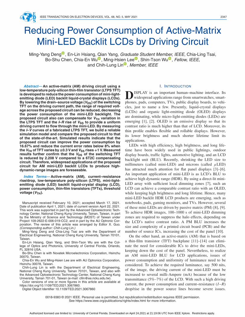
Fig. 2. Diode-connected scheme used in AMOLED pixel circuit.
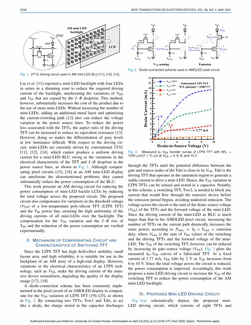
Fig. 3. Measured ID–VDS transfer curves of LTPS TFT with W/L =1040 µm/(7 + 7) µm at VGS = 4, 6, 8, and 10 V.
through the TFTs until the potential difference between thegate and source nodes of the Tdri is close to its VTH. Tdri is thedriving TFT that operates in the saturation region to generate astable current to drive a mini-LED. Hence, the VTH variation inLTPS TFTs can be sensed and stored in a capacitor. Notably,in this scheme, a switching TFT, Tsw2, is needed to block anycurrent that would flow through the emissive device beforethe emission period begins, avoiding undesired emission. Thevoltage across the circuit is the sum of the drain–source voltage(VDS) of the TFTs and the forward voltage of the mini-LED.Since the driving current of the mini-LED as BLU is muchlarger than that in the AMOLED pixel circuit, increasing thenumber of TFTs on the current path drastically increases thestatic power, according to Pstatic = ID × Vtotal × emissionduty, where Vtotal is the sum of VDS values of the switchingand the driving TFTs and the forward voltage of the mini-LED. The VDS of the switching TFT, however, can be reducedby increasing its gate–source voltage (VGS). Fig. 3 plots themeasured ID–VDS curves of a fabricated TFT. At a fixedcurrent of 1.77 mA, VDS falls by 2 V as VGS increases from6 to 10 V. Since the total voltage across the circuit is reduced,the power consumption is improved. Accordingly, this workproposes a mini-LED driving circuit to increase the VGS of theswitching TFT to reduce the power consumption of the AMmini-LED backlight.
III. PROPOSED MINI-LED DRIVING CIRCUIT
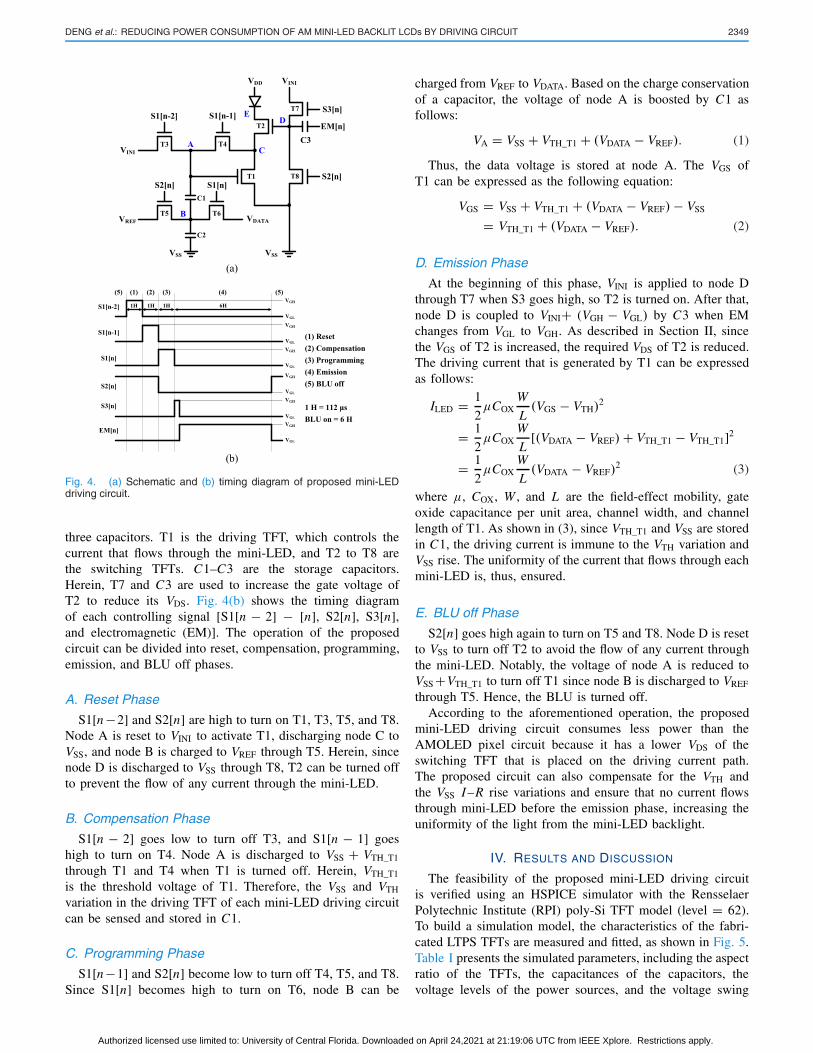
Fig. 4(a) schematically depicts the proposed mini-LED driving circuit, which consists of eight TFTs and
Authorized licensed use limited to: University of Central Florida. Downloaded on April 24,2021 at 21:19:06 UTC from IEEE Xplore. Restrictions apply.
DENG et al.: REDUCING POWER CONSUMPTION OF AM MINI-LED BACKLIT LCDs BY DRIVING CIRCUIT 2349
Fig. 4. (a) Schematic and (b) timing diagram of proposed mini-LEDdriving circuit.
three capacitors. T1 is the driving TFT, which controls thecurrent that flows through the mini-LED, and T2 to T8 arethe switching TFTs. C1–C3 are the storage capacitors.Herein, T7 and C3 are used to increase the gate voltage ofT2 to reduce its VDS. Fig. 4(b) shows the timing diagramof each controlling signal [S1[n − 2] − [n], S2[n], S3[n],and electromagnetic (EM)]. The operation of the proposedcircuit can be divided into reset, compensation, programming,emission, and BLU off phases.
A. Reset Phase
S1[n −2] and S2[n] are high to turn on T1, T3, T5, and T8.Node A is reset to VINI to activate T1, discharging node C toVSS, and node B is charged to VREF through T5. Herein, sincenode D is discharged to VSS through T8, T2 can be turned offto prevent the flow of any current through the mini-LED.
B. Compensation Phase
S1[n − 2] goes low to turn off T3, and S1[n − 1] goeshigh to turn on T4. Node A is discharged to VSS + VTH_T1
through T1 and T4 when T1 is turned off. Herein, VTH_T1
is the threshold voltage of T1. Therefore, the VSS and VTH
variation in the driving TFT of each mini-LED driving circuitcan be sensed and stored in C1.
C. Programming Phase
S1[n−1] and S2[n] become low to turn off T4, T5, and T8.Since S1[n] becomes high to turn on T6, node B can be
charged from VREF to VDATA. Based on the charge conservationof a capacitor, the voltage of node A is boosted by C1 asfollows:
VA = VSS + VTH_T1 + (VDATA − VREF). (1)
Thus, the data voltage is stored at node A. The VGS ofT1 can be expressed as the following equation:
VGS = VSS + VTH_T1 + (VDATA − VREF) − VSS
= VTH_T1 + (VDATA − VREF). (2)
D. Emission Phase
At the beginning of this phase, VINI is applied to node Dthrough T7 when S3 goes high, so T2 is turned on. After that,node D is coupled to VINI+ (VGH − VGL) by C3 when EMchanges from VGL to VGH. As described in Section II, sincethe VGS of T2 is increased, the required VDS of T2 is reduced.The driving current that is generated by T1 can be expressedas follows:
ILED = 1
2µCOX
W
L(VGS − VTH)2
= 1
2µCOX
W
L[(VDATA − VREF) + VTH_T1 − VTH_T1]2
= 1
2µCOX
W
L(VDATA − VREF)
2 (3)
where µ, COX, W , and L are the field-effect mobility, gateoxide capacitance per unit area, channel width, and channellength of T1. As shown in (3), since VTH_T1 and VSS are storedin C1, the driving current is immune to the VTH variation andVSS rise. The uniformity of the current that flows through eachmini-LED is, thus, ensured.
E. BLU off Phase
S2[n] goes high again to turn on T5 and T8. Node D is resetto VSS to turn off T2 to avoid the flow of any current throughthe mini-LED. Notably, the voltage of node A is reduced toVSS +VTH_T1 to turn off T1 since node B is discharged to VREF
through T5. Hence, the BLU is turned off.According to the aforementioned operation, the proposed
mini-LED driving circuit consumes less power than theAMOLED pixel circuit because it has a lower VDS of theswitching TFT that is placed on the driving current path.The proposed circuit can also compensate for the VTH andthe VSS I–R rise variations and ensure that no current flowsthrough mini-LED before the emission phase, increasing theuniformity of the light from the mini-LED backlight.
IV. RESULTS AND DISCUSSION
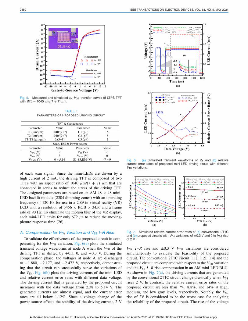
The feasibility of the proposed mini-LED driving circuitis verified using an HSPICE simulator with the RensselaerPolytechnic Institute (RPI) poly-Si TFT model (level = 62).To build a simulation model, the characteristics of the fabri-cated LTPS TFTs are measured and fitted, as shown in Fig. 5.Table I presents the simulated parameters, including the aspectratio of the TFTs, the capacitances of the capacitors, thevoltage levels of the power sources, and the voltage swing
Authorized licensed use limited to: University of Central Florida. Downloaded on April 24,2021 at 21:19:06 UTC from IEEE Xplore. Restrictions apply.
2350 IEEE TRANSACTIONS ON ELECTRON DEVICES, VOL. 68, NO. 5, MAY 2021
Fig. 5. Measured and simulated ID–VGS transfer curves of LTPS TFTwith W/L = 1040 µm/(7 + 7) µm.
TABLE IPARAMETERS OF PROPOSED DRIVING CIRCUIT
of each scan signal. Since the mini-LEDs are driven by ahigh current of 2 mA, the driving TFT is composed of twoTFTs with an aspect ratio of 1040 µm/(7 + 7) µm that areconnected in series to reduce the stress of the driving TFT.The designed parameters are based on an AM 48 × 48 mini-LED backlit module (2304 dimming zones) with an operatingfrequency of 120 Hz for use in a 2.89-in virtual reality (VR)LCD with a resolution of 3456 × RGB × 3456 and a framerate of 90 Hz. To eliminate the motion blur of the VR display,each mini-LED emits for only 672 µs to reduce the moving-picture response time [26].
A. Compensation for VTH Variation and VSS I–R Rise
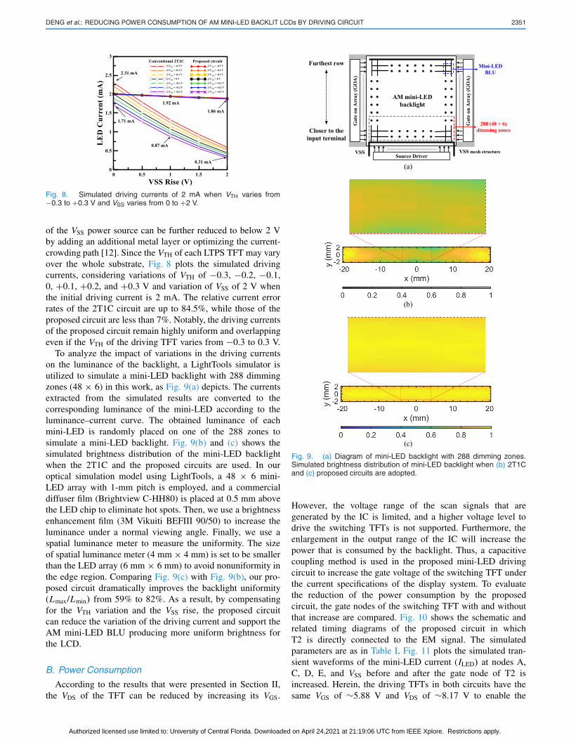
To validate the effectiveness of the proposed circuit in com-pensating for the VTH variation, Fig. 6(a) plots the simulatedtransient voltage waveforms at node A when the VTH of thedriving TFT is shifted by +0.3, 0, and −0.3 V. During thecompensation phase, the voltages at node A are dischargedto −1.880, −2.177, and −2.472 V, respectively, demonstrat-ing that the circuit can successfully sense the variations ofthe VTH. Fig. 6(b) plots the driving currents of the mini-LEDand relative current error rates with different data voltage.The driving current that is generated by the proposed circuitincreases with the data voltage from 2.38 to 5.14 V. Thegenerated currents are almost equal, and the current errorrates are all below 1.12%. Since a voltage change of thepower source affects the stability of the driving current, 2 V
Fig. 6. (a) Simulated transient waveforms of VA and (b) relativecurrent error rates of proposed mini-LED driving circuit with differentVTH variations.
Fig. 7. Simulated relative current error rates of (a) conventional 2T1Cand (b) proposed circuits with VTH variations of ±0.3 V and 0 to VSS riseof 2 V.
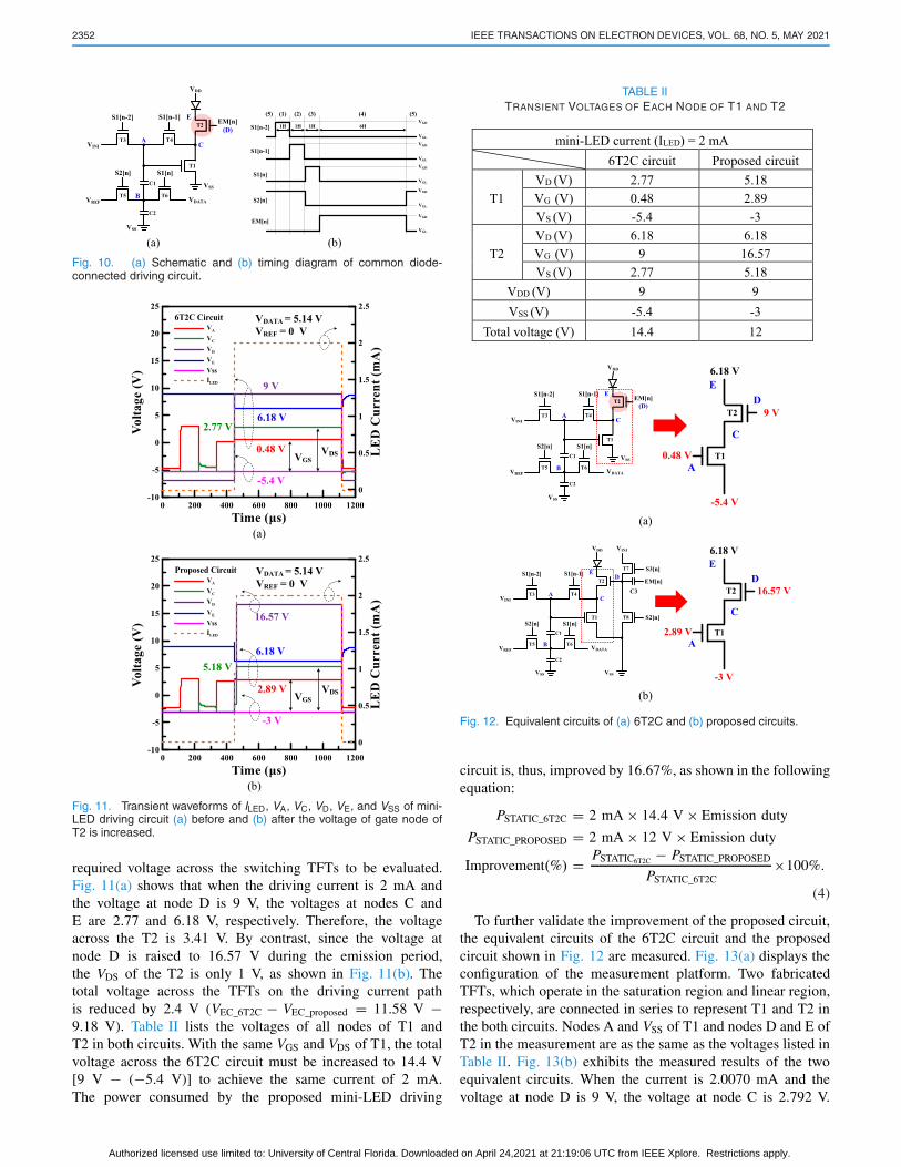
VSS I–R rise and ±0.3 V VTH variations are consideredsimultaneously to evaluate the feasibility of the proposedcircuit. The conventional 2T1C circuit [11], [12], [14] and theproposed circuit are compared with respect to the VTH variationand the VSS I–R rise compensation in an AM mini-LED BLU.As shown in Fig. 7(a), the driving currents that are generatedby the conventional 2T1C circuit change drastically when VSS
rises 2 V. In contrast, the relative current error rates of theproposed circuit are less than 7%, 8.8%, and 14% at high,medium, and low gray levels, respectively. Notably, the VSS
rise of 2V is considered to be the worst case for analyzingthe reliability of the proposed circuit. The rise of the voltage
Authorized licensed use limited to: University of Central Florida. Downloaded on April 24,2021 at 21:19:06 UTC from IEEE Xplore. Restrictions apply.
DENG et al.: REDUCING POWER CONSUMPTION OF AM MINI-LED BACKLIT LCDs BY DRIVING CIRCUIT 2351
Fig. 8. Simulated driving currents of 2 mA when VTH varies from−0.3 to +0.3 V and VSS varies from 0 to +2 V.
of the VSS power source can be further reduced to below 2 Vby adding an additional metal layer or optimizing the current-crowding path [12]. Since the VTH of each LTPS TFT may varyover the whole substrate, Fig. 8 plots the simulated drivingcurrents, considering variations of VTH of −0.3, −0.2, −0.1,0, +0.1, +0.2, and +0.3 V and variation of VSS of 2 V whenthe initial driving current is 2 mA. The relative current errorrates of the 2T1C circuit are up to 84.5%, while those of theproposed circuit are less than 7%. Notably, the driving currentsof the proposed circuit remain highly uniform and overlappingeven if the VTH of the driving TFT varies from −0.3 to 0.3 V.
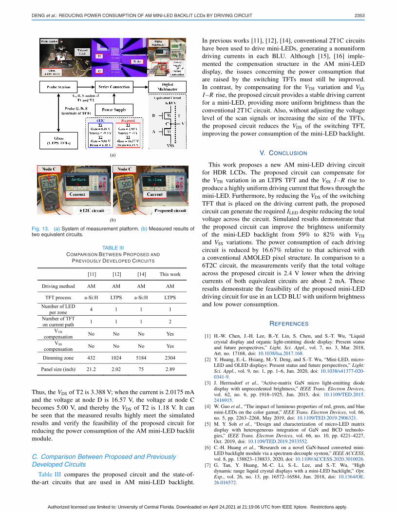
To analyze the impact of variations in the driving currentson the luminance of the backlight, a LightTools simulator isutilized to simulate a mini-LED backlight with 288 dimmingzones (48 × 6) in this work, as Fig. 9(a) depicts. The currentsextracted from the simulated results are converted to thecorresponding luminance of the mini-LED according to theluminance–current curve. The obtained luminance of eachmini-LED is randomly placed on one of the 288 zones tosimulate a mini-LED backlight. Fig. 9(b) and (c) shows thesimulated brightness distribution of the mini-LED backlightwhen the 2T1C and the proposed circuits are used. In ouroptical simulation model using LightTools, a 48 × 6 mini-LED array with 1-mm pitch is employed, and a commercialdiffuser film (Brightview C-HH80) is placed at 0.5 mm abovethe LED chip to eliminate hot spots. Then, we use a brightnessenhancement film (3M Vikuiti BEFIII 90/50) to increase theluminance under a normal viewing angle. Finally, we use aspatial luminance meter to measure the uniformity. The sizeof spatial luminance meter (4 mm × 4 mm) is set to be smallerthan the LED array (6 mm × 6 mm) to avoid nonuniformity inthe edge region. Comparing Fig. 9(c) with Fig. 9(b), our pro-posed circuit dramatically improves the backlight uniformity(Lmax/Lmin) from 59% to 82%. As a result, by compensatingfor the VTH variation and the VSS rise, the proposed circuitcan reduce the variation of the driving current and support theAM mini-LED BLU producing more uniform brightness forthe LCD.
B. Power Consumption
According to the results that were presented in Section II,the VDS of the TFT can be reduced by increasing its VGS.
Fig. 9. (a) Diagram of mini-LED backlight with 288 dimming zones.Simulated brightness distribution of mini-LED backlight when (b) 2T1Cand (c) proposed circuits are adopted.
However, the voltage range of the scan signals that aregenerated by the IC is limited, and a higher voltage level todrive the switching TFTs is not supported. Furthermore, theenlargement in the output range of the IC will increase thepower that is consumed by the backlight. Thus, a capacitivecoupling method is used in the proposed mini-LED drivingcircuit to increase the gate voltage of the switching TFT underthe current specifications of the display system. To evaluatethe reduction of the power consumption by the proposedcircuit, the gate nodes of the switching TFT with and withoutthat increase are compared. Fig. 10 shows the schematic andrelated timing diagrams of the proposed circuit in whichT2 is directly connected to the EM signal. The simulatedparameters are as in Table I. Fig. 11 plots the simulated tran-sient waveforms of the mini-LED current (ILED) at nodes A,C, D, E, and VSS before and after the gate node of T2 isincreased. Herein, the driving TFTs in both circuits have thesame VGS of ∼5.88 V and VDS of ∼8.17 V to enable the
Authorized licensed use limited to: University of Central Florida. Downloaded on April 24,2021 at 21:19:06 UTC from IEEE Xplore. Restrictions apply.
2352 IEEE TRANSACTIONS ON ELECTRON DEVICES, VOL. 68, NO. 5, MAY 2021
Fig. 10. (a) Schematic and (b) timing diagram of common diode-connected driving circuit.
Fig. 11. Transient waveforms of ILED, VA, VC, VD, VE, and VSS of mini-LED driving circuit (a) before and (b) after the voltage of gate node ofT2 is increased.
required voltage across the switching TFTs to be evaluated.Fig. 11(a) shows that when the driving current is 2 mA andthe voltage at node D is 9 V, the voltages at nodes C andE are 2.77 and 6.18 V, respectively. Therefore, the voltageacross the T2 is 3.41 V. By contrast, since the voltage atnode D is raised to 16.57 V during the emission period,the VDS of the T2 is only 1 V, as shown in Fig. 11(b). Thetotal voltage across the TFTs on the driving current pathis reduced by 2.4 V (VEC_6T2C − VEC_proposed = 11.58 V −9.18 V). Table II lists the voltages of all nodes of T1 andT2 in both circuits. With the same VGS and VDS of T1, the totalvoltage across the 6T2C circuit must be increased to 14.4 V[9 V − (−5.4 V)] to achieve the same current of 2 mA.The power consumed by the proposed mini-LED driving
TABLE IITRANSIENT VOLTAGES OF EACH NODE OF T1 AND T2
Fig. 12. Equivalent circuits of (a) 6T2C and (b) proposed circuits.
circuit is, thus, improved by 16.67%, as shown in the followingequation:
PSTATIC_6T2C = 2 mA × 14.4 V × Emission duty
PSTATIC_PROPOSED = 2 mA × 12 V × Emission duty
Improvement(%) = PSTATIC6T2C − PSTATIC_PROPOSED
PSTATIC_6T2C×100%.
(4)
To further validate the improvement of the proposed circuit,the equivalent circuits of the 6T2C circuit and the proposedcircuit shown in Fig. 12 are measured. Fig. 13(a) displays theconfiguration of the measurement platform. Two fabricatedTFTs, which operate in the saturation region and linear region,respectively, are connected in series to represent T1 and T2 inthe both circuits. Nodes A and VSS of T1 and nodes D and E ofT2 in the measurement are as the same as the voltages listed inTable II. Fig. 13(b) exhibits the measured results of the twoequivalent circuits. When the current is 2.0070 mA and thevoltage at node D is 9 V, the voltage at node C is 2.792 V.
Authorized licensed use limited to: University of Central Florida. Downloaded on April 24,2021 at 21:19:06 UTC from IEEE Xplore. Restrictions apply.
DENG et al.: REDUCING POWER CONSUMPTION OF AM MINI-LED BACKLIT LCDs BY DRIVING CIRCUIT 2353
Fig. 13. (a) System of measurement platform. (b) Measured results oftwo equivalent circuits.
TABLE IIICOMPARISON BETWEEN PROPOSED AND
PREVIOUSLY DEVELOPED CIRCUITS
Thus, the VDS of T2 is 3.388 V; when the current is 2.0175 mAand the voltage at node D is 16.57 V, the voltage at node Cbecomes 5.00 V, and thereby the VDS of T2 is 1.18 V. It canbe seen that the measured results highly meet the simulatedresults and verify the feasibility of the proposed circuit forreducing the power consumption of the AM mini-LED backlitmodule.
C. Comparison Between Proposed and PreviouslyDeveloped Circuits
Table III compares the proposed circuit and the state-of-the-art circuits that are used in AM mini-LED backlight.
In previous works [11], [12], [14], conventional 2T1C circuitshave been used to drive mini-LEDs, generating a nonuniformdriving currents in each BLU. Although [15], [16] imple-mented the compensation structure in the AM mini-LEDdisplay, the issues concerning the power consumption thatare raised by the switching TFTs must still be improved.In contrast, by compensating for the VTH variation and VSS
I–R rise, the proposed circuit provides a stable driving currentfor a mini-LED, providing more uniform brightness than theconventional 2T1C circuit. Also, without adjusting the voltagelevel of the scan signals or increasing the size of the TFTs,the proposed circuit reduces the VDS of the switching TFT,improving the power consumption of the mini-LED backlight.
V. CONCLUSION
This work proposes a new AM mini-LED driving circuitfor HDR LCDs. The proposed circuit can compensate forthe VTH variation in an LTPS TFT and the VSS I–R rise toproduce a highly uniform driving current that flows through themini-LED. Furthermore, by reducing the VDS of the switchingTFT that is placed on the driving current path, the proposedcircuit can generate the required ILED despite reducing the totalvoltage across the circuit. Simulated results demonstrate thatthe proposed circuit can improve the brightness uniformityof the mini-LED backlight from 59% to 82% with VTH
and VSS variations. The power consumption of each drivingcircuit is reduced by 16.67% relative to that achieved witha conventional AMOLED pixel structure. In comparison to a6T2C circuit, the measurements verify that the total voltageacross the proposed circuit is 2.4 V lower when the drivingcurrents of both equivalent circuits are about 2 mA. Theseresults demonstrate the feasibility of the proposed mini-LEDdriving circuit for use in an LCD BLU with uniform brightnessand low power consumption.
REFERENCES
[1] H.-W. Chen, J.-H. Lee, B.-Y. Lin, S. Chen, and S.-T. Wu, “Liquidcrystal display and organic light-emitting diode display: Present statusand future perspectives,” Light, Sci. Appl., vol. 7, no. 3, Mar. 2018,Art. no. 17168, doi: 10.1038/lsa.2017.168.
[2] Y. Huang, E.-L. Hsiang, M.-Y. Deng, and S.-T. Wu, “Mini-LED, micro-LED and OLED displays: Present status and future perspectives,” Light:Sci. Appl., vol. 9, no. 1, pp. 1–6, Jun. 2020, doi: 10.1038/s41377-020-0341-9.
[3] J. Herrnsdorf et al., “Active-matrix GaN micro light-emitting diodedisplay with unprecedented brightness,” IEEE Trans. Electron Devices,vol. 62, no. 6, pp. 1918–1925, Jun. 2015, doi: 10.1109/TED.2015.2416915.
[4] W. Guo et al., “The impact of luminous properties of red, green, and bluemini-LEDs on the color gamut,” IEEE Trans. Electron Devices, vol. 66,no. 5, pp. 2263–2268, May 2019, doi: 10.1109/TED.2019.2906321.
[5] M. Y. Soh et al., “Design and characterization of micro-LED matrixdisplay with heterogeneous integration of GaN and BCD technolo-gies,” IEEE Trans. Electron Devices, vol. 66, no. 10, pp. 4221–4227,Oct. 2019, doi: 10.1109/TED.2019.2933552.
[6] C.-H. Huang et al., “Research on a novel GaN-based converted mini-LED backlight module via a spectrum-decouple system,” IEEE ACCESS,vol. 8, pp. 138823–138833, 2020, doi: 10.1109/ACCESS.2020.3010026.
[7] G. Tan, Y. Huang, M.-C. Li, S.-L. Lee, and S.-T. Wu, “Highdynamic range liquid crystal displays with a mini-LED backlight,” Opt.Exp., vol. 26, no. 13, pp. 16572–16584, Jun. 2018, doi: 10.1364/OE.26.016572.
Authorized licensed use limited to: University of Central Florida. Downloaded on April 24,2021 at 21:19:06 UTC from IEEE Xplore. Restrictions apply.
2354 IEEE TRANSACTIONS ON ELECTRON DEVICES, VOL. 68, NO. 5, MAY 2021
[8] T. Masuda et al., “28-3: Mini-LED backlight for HDR compati-ble mobile displays,” in SID Symp. Dig. Tech. Papers, Jun. 2019,pp. 390–393, doi: 10.1002/sdtp.12939.
[9] E. Guan et al., “17-3: A novel pixel-level local dimming back-light system for HDR display based on mini-LED,” in SID Symp.Dig. Tech. Papers, Aug. 2020, pp. 231–234, doi: 10.1002/sdtp.13846.
[10] C.-L. Ting, C.-K. Wei, K.-Y. Kao, L.-W. Mau, H.-T. Chen,and M. Shibazaki, “Active matrix driving mini-LED device,”in IDW Tech. Dig., 2019, pp. 425–428, doi: 10.36463/idw.2019.0425.
[11] B. Liu et al., “An active matrix mini-LEDs backlight based on a-SiTFT,” in IDW Tech. Dig., Jul. 2019, pp. 652–654.
[12] Y.-E. Wu, M.-H. Lee, Y.-C. Lin, C. Kuo, Y.-H. Lin, and W.-M. Huang,“Active matrix mini-LED backlights for 1000PPI VR LCD,” in SIDSymp. Dig. Tech. Papers, Jun. 2019, pp. 562–565, doi: 10.1002/sdtp.12982.
[13] J.-J. Su et al., “An overview of solutions for achieving HDR LCDs,”in SID Symp. Dig. Tech. Papers, 2020, pp. 224–227, doi: 10.1002/sdtp.13844.
[14] H. Xu et al., “AM MLED backlight units on glass for 75-inch LCDdisplays,” in SID Symp. Dig. Tech. Papers, 2020, pp. 122–125, doi:10.1002/sdtp.13820.
[15] W.-S. Shin et al., “A driving method of pixel circuit using a-IGZOTFT for suppression of threshold voltage shift in AMLED displays,”IEEE Electron Device Lett., vol. 38, no. 6, pp. 760–762, Jun. 2017, doi:10.1109/LED.2017.2699669.
[16] B. Liu, Q. Liu, J. Liu, F. Zhu, and H. Zhou, “A new compensationpixel circuit based on a-Si TFTs,” in Proc. IEEE Int. Conf. Elec-tron. Technol., May 2020, pp. 123–126, doi: 10.1109/ICET49382.2020.9119591.
[17] C.-L. Lin, C.-C. Hung, P.-S. Chen, P.-C. Lai, and M.-H. Cheng, “Newvoltage-programmed AMOLED pixel circuit to compensate for nonuni-form electrical characteristics of LTPS TFTs and voltage drop in powerline,” IEEE Trans. Electron Devices, vol. 61, no. 7, pp. 2454–2458,Jul. 2014, doi: 10.1109/TED.2014.2325612.
[18] Y.-H. Tai, C.-H. Lin, S. Yeh, C.-C. Tu, and K. S. Karim, “LTPSactive pixel circuit with threshold voltage compensation for X-rayimaging applications,” IEEE Trans. Electron Devices, vol. 66, no. 10,pp. 4216–4220, Oct. 2019, doi: 10.1109/TED.2019.2933225.
[19] M. Bagheri, S. J. Ashitani, and A. Nathan, “Fast voltage-programmedpixel architecture for AMOLED displays,” J. Display Technol., vol. 6,no. 5, pp. 191–195, May 2010, doi: 10.1109/JDT.2010.2044015.
[20] C.-L. Lin, C.-C. Hung, W.-Y. Chang, M.-H. Cheng, P.-Y. Kuo, andY.-C. Chen, “Voltage driving scheme using three TFTs and onecapacitor for active-matrix organic light-emitting diode pixel circuits,”J. Display Technol., vol. 8, no. 10, pp. 602–608, Oct. 2012, doi:10.1109/jdt.2012.2209110.
[21] C.-L. Lin, C.-C. Hung, P.-Y. Kuo, and M.-H. Cheng, “New LTPS pixelcircuit with AC driving method to reduce OLED degradation for 3DAMOLED displays,” J. Display Technol., vol. 8, no. 12, pp. 681–683,Dec. 2012, doi: 10.1109/JDT.2012.2225017.
[22] W.-J. Wu et al., “High-speed voltage-programmed pixel circuit forAMOLED displays employing threshold voltage one-time detectionmethod,” IEEE Electron Device Lett., vol. 34, no. 9, pp. 1148–1150,Sep. 2013, doi: 10.1109/LED.2013.2271908.
[23] J.-P. Lee, H.-S. Jeon, D.-S. Moon, and B. S. Bae, “Threshold voltageand IR drop compensation of an AMOLED pixel circuit without a VDDline,” IEEE Electron Device Lett., vol. 35, no. 1, pp. 72–74, Jan. 2014,doi: 10.1109/LED.2013.2289315.
[24] C.-L. Lin, Y.-T. Liu, C.-E. Lee, P.-S. Chen, T.-C. Chu, and C.-C. Hung,“A-InGaZnO active-matrix organic LED pixel periodically detectingthin-film transistor threshold voltage once for multiple frames,” IEEEElectron Device Lett., vol. 36, no. 11, pp. 1166–1168, Nov. 2015, doi:10.1109/LED.2015.2480861.
[25] N.-H. Keum, S.-K. Hong, and O.-K. Kwon, “An AMOLED pixel circuitwith a compensating scheme for variations in subthreshold slope andthreshold voltage of driving TFTs,” IEEE J. Solid-State Circuits, vol. 55,no. 11, pp. 3087–3096, Nov. 2020, doi: 10.1109/JSSC.2020.3014149.
[26] F. Gou, H. Chen, M.-C. Li, S.-L. Lee, and S.-T. Wu, “Motion-blur-freeLCD for high-resolution virtual reality displays,” J. Soc. Inf. Display,vol. 26, no. 4, pp. 223–228, Apr. 2018, doi: 10.1002/jsid.662.
Authorized licensed use limited to: University of Central Florida. Downloaded on April 24,2021 at 21:19:06 UTC from IEEE Xplore. Restrictions apply.