Embed Size (px)
Citation preview

Reconfigurable Field Programmable Gate Arraysfor Mission-Critical Applications

Niccolò Battezzati · Luca Sterpone · Massimo Violante
Reconfigurable FieldProgrammable Gate Arraysfor Mission-CriticalApplications
123

Niccolò BattezzatiDipto. Automatica e InformaticaPolitecnico di TorinoCorso Duca degli Abruzzi 2410129 Torino, [email protected]
Luca SterponePolitecnico di TorinoCorso Duca Degli Abruzzi 2410129 Torino, [email protected]
Massimo ViolanteDipto. Automatica e InformaticaPolitecnico di TorinoCorso Duca degli Abruzzi 2410129 Torino, [email protected]
ISBN 978-1-4419-7594-2 e-ISBN 978-1-4419-7595-9DOI 10.1007/978-1-4419-7595-9Springer New York Dordrecht Heidelberg London
Library of Congress Control Number: 2010938708
c© Springer Science+Business Media, LLC 2011All rights reserved. This work may not be translated or copied in whole or in part without the writtenpermission of the publisher (Springer Science+Business Media, LLC, 233 Spring Street, New York,NY 10013, USA), except for brief excerpts in connection with reviews or scholarly analysis. Use inconnection with any form of information storage and retrieval, electronic adaptation, computersoftware, or by similar or dissimilar methodology now known or hereafter developed is forbidden.The use in this publication of trade names, trademarks, service marks, and similar terms, even ifthey are not identified as such, is not to be taken as an expression of opinion as to whether or notthey are subject to proprietary rights.
Printed on acid-free paper
Springer is part of Springer Science+Business Media (www.springer.com)
Contents
1 Introduction . . . . . . . . . . . . . . . . . . . . . . . . . . . . . . . . . . . . . . . . . . . . . . . . . . . 1References . . . . . . . . . . . . . . . . . . . . . . . . . . . . . . . . . . . . . . . . . . . . . . . . . . . . . . 4
Part I Basic Concepts
2 Reconfigurable Field Programmable Gate Arrays: Basic Concepts . . . 72.1 FPGA Architectures . . . . . . . . . . . . . . . . . . . . . . . . . . . . . . . . . . . . . . . . . 72.2 FPGA Configuration Technology . . . . . . . . . . . . . . . . . . . . . . . . . . . . . . 12
2.2.1 Floating Gate Technology . . . . . . . . . . . . . . . . . . . . . . . . . . . . 122.2.2 Antifuse Technology . . . . . . . . . . . . . . . . . . . . . . . . . . . . . . . . . 132.2.3 SRAM Technology . . . . . . . . . . . . . . . . . . . . . . . . . . . . . . . . . . 13
2.3 The Logic Block . . . . . . . . . . . . . . . . . . . . . . . . . . . . . . . . . . . . . . . . . . . . 142.3.1 Fine-Grain Logic Blocks . . . . . . . . . . . . . . . . . . . . . . . . . . . . . 142.3.2 Coarse-Grain Logic Blocks . . . . . . . . . . . . . . . . . . . . . . . . . . . 15
2.4 The Routing Architecture . . . . . . . . . . . . . . . . . . . . . . . . . . . . . . . . . . . . 172.4.1 The Switching Elements . . . . . . . . . . . . . . . . . . . . . . . . . . . . . . 18
2.5 The Input/Output Blocks . . . . . . . . . . . . . . . . . . . . . . . . . . . . . . . . . . . . . 212.6 The Configuration Memory . . . . . . . . . . . . . . . . . . . . . . . . . . . . . . . . . . . 212.7 An Overview of the Architecture of Modern FPGAs . . . . . . . . . . . . . . 23
2.7.1 Logic Resources . . . . . . . . . . . . . . . . . . . . . . . . . . . . . . . . . . . . 242.7.2 Interconnection Resources . . . . . . . . . . . . . . . . . . . . . . . . . . . . 272.7.3 Memory Resources . . . . . . . . . . . . . . . . . . . . . . . . . . . . . . . . . . 302.7.4 Arithmetic Resources . . . . . . . . . . . . . . . . . . . . . . . . . . . . . . . . 312.7.5 Processing Resources . . . . . . . . . . . . . . . . . . . . . . . . . . . . . . . . 312.7.6 Interfacing Resources . . . . . . . . . . . . . . . . . . . . . . . . . . . . . . . . 34
References . . . . . . . . . . . . . . . . . . . . . . . . . . . . . . . . . . . . . . . . . . . . . . . . . . . . . . 34
3 Reconfigurable Field Programmable Gate Arrays: Failure Modesand Analysis . . . . . . . . . . . . . . . . . . . . . . . . . . . . . . . . . . . . . . . . . . . . . . . . . . . 373.1 The Impact of the Environment on the Device . . . . . . . . . . . . . . . . . . . 37
3.1.1 Radiation Environments . . . . . . . . . . . . . . . . . . . . . . . . . . . . . . 38
v

vi Contents
3.1.2 Radiation Characteristics . . . . . . . . . . . . . . . . . . . . . . . . . . . . . 403.1.3 Physical Effects . . . . . . . . . . . . . . . . . . . . . . . . . . . . . . . . . . . . . 413.1.4 From the Effect to the Fault . . . . . . . . . . . . . . . . . . . . . . . . . . . 443.1.5 Fault Models in FPGAs . . . . . . . . . . . . . . . . . . . . . . . . . . . . . . 503.1.6 SEUs and MCUs Effects on the FPGA’s Routing Resources 523.1.7 SEUs and MCUs Effects on the FPGA’s Logic Resources . . 573.1.8 Topological Modifications Induced by SEUs and MCUs . . . 58
3.2 Analysis Techniques . . . . . . . . . . . . . . . . . . . . . . . . . . . . . . . . . . . . . . . . 623.2.1 Life Testing . . . . . . . . . . . . . . . . . . . . . . . . . . . . . . . . . . . . . . . . 643.2.2 Accelerated Radiation Testing . . . . . . . . . . . . . . . . . . . . . . . . . 663.2.3 Fault Injection . . . . . . . . . . . . . . . . . . . . . . . . . . . . . . . . . . . . . . 683.2.4 Analytical Techniques . . . . . . . . . . . . . . . . . . . . . . . . . . . . . . . . 74
References . . . . . . . . . . . . . . . . . . . . . . . . . . . . . . . . . . . . . . . . . . . . . . . . . . . . . . 82
4 Reconfigurable Field Programmable Gate Arrays: HardeningSolutions . . . . . . . . . . . . . . . . . . . . . . . . . . . . . . . . . . . . . . . . . . . . . . . . . . . . . . 854.1 Overview on the Design Process for FPGA Applications . . . . . . . . . . 85
4.1.1 FPGA Design . . . . . . . . . . . . . . . . . . . . . . . . . . . . . . . . . . . . . . . 874.1.2 Application Design . . . . . . . . . . . . . . . . . . . . . . . . . . . . . . . . . . 88
4.2 Techniques for FPGA Manufacturer . . . . . . . . . . . . . . . . . . . . . . . . . . . 964.2.1 Mitigation Techniques for SEL . . . . . . . . . . . . . . . . . . . . . . . . 974.2.2 Mitigation Techniques for TID . . . . . . . . . . . . . . . . . . . . . . . . 1044.2.3 Mitigation Techniques for Single Memory Elements . . . . . . 1064.2.4 Mitigation Techniques for Programming Elements . . . . . . . . 1134.2.5 Mitigation Techniques for Memories . . . . . . . . . . . . . . . . . . . 1204.2.6 Mitigation Techniques for Logic Elements . . . . . . . . . . . . . . . 1224.2.7 Mitigation Techniques for Input/Output Elements . . . . . . . . . 124
4.3 Overview of Techniques for FPGA User . . . . . . . . . . . . . . . . . . . . . . . . 1264.3.1 In-Chip Mitigation Techniques . . . . . . . . . . . . . . . . . . . . . . . . 1264.3.2 Off-Chip Mitigation Techniques . . . . . . . . . . . . . . . . . . . . . . . 167
References . . . . . . . . . . . . . . . . . . . . . . . . . . . . . . . . . . . . . . . . . . . . . . . . . . . . . . 168
Part II Practical Concepts
5 Reprogrammable FPGAs for Mission-Critical Applications . . . . . . . . . 1795.1 Introduction . . . . . . . . . . . . . . . . . . . . . . . . . . . . . . . . . . . . . . . . . . . . . . . . 1795.2 Radiation-Tolerant Reprogrammable FPGAs . . . . . . . . . . . . . . . . . . . . 180
5.2.1 Virtex-4 QV Products . . . . . . . . . . . . . . . . . . . . . . . . . . . . . . . . 1805.2.2 Actel RT ProASIC3 . . . . . . . . . . . . . . . . . . . . . . . . . . . . . . . . . 182
5.3 Radiation-Hardened Re-programmable FPGAs . . . . . . . . . . . . . . . . . . 1845.3.1 Atmel ATF280 . . . . . . . . . . . . . . . . . . . . . . . . . . . . . . . . . . . . . . 184
References . . . . . . . . . . . . . . . . . . . . . . . . . . . . . . . . . . . . . . . . . . . . . . . . . . . . . . 186

Contents vii
6 Putting Mitigation Techniques at Work . . . . . . . . . . . . . . . . . . . . . . . . . . . 1876.1 Mitigation Techniques for SRAM-Based Devices: The Xilinx
Virtex Case Study . . . . . . . . . . . . . . . . . . . . . . . . . . . . . . . . . . . . . . . . . . 1876.1.1 Single Event Upsets Consideration . . . . . . . . . . . . . . . . . . . . . 1876.1.2 Multiple Cell Upsets Considerations . . . . . . . . . . . . . . . . . . . . 192
6.2 Mitigation Techniques for Flash-Based Devices:The Actel ProASIC3 Case Study . . . . . . . . . . . . . . . . . . . . . . . . . . . . . 1986.2.1 Single Event Transient Characterization . . . . . . . . . . . . . . . . . 1986.2.2 Single Event Transient Mitigation . . . . . . . . . . . . . . . . . . . . . . 201
References . . . . . . . . . . . . . . . . . . . . . . . . . . . . . . . . . . . . . . . . . . . . . . . . . . . . . . 204
7 System-Level Considerations . . . . . . . . . . . . . . . . . . . . . . . . . . . . . . . . . . . . 2057.1 Introduction . . . . . . . . . . . . . . . . . . . . . . . . . . . . . . . . . . . . . . . . . . . . . . . . 2057.2 The Target Radioactive Environment . . . . . . . . . . . . . . . . . . . . . . . . . . . 2067.3 The Impact of the Target Radioactive Environment . . . . . . . . . . . . . . . 2087.4 The Impact of the Target Application . . . . . . . . . . . . . . . . . . . . . . . . . . 2097.5 System-Level Considerations . . . . . . . . . . . . . . . . . . . . . . . . . . . . . . . . . 211References . . . . . . . . . . . . . . . . . . . . . . . . . . . . . . . . . . . . . . . . . . . . . . . . . . . . . . 212
8 Conclusions . . . . . . . . . . . . . . . . . . . . . . . . . . . . . . . . . . . . . . . . . . . . . . . . . . . . 213
Subject Index . . . . . . . . . . . . . . . . . . . . . . . . . . . . . . . . . . . . . . . . . . . . . . . . . . . . . . 217

Chapter 1Introduction
Field-programmable gate arrays (FPGAs) play an important role in a growingnumber of applications. Originally devised to implement simple logic functions,FPGAs are today able to implement entire systems on a single chip. The mostadvanced FPGA devices as the Xilinx Virtex-7 family [3] are now offering up to2 million logic cells, 65 Mb of embedded memory, and a number of additionalfeatures such as high-performance arithmetic functions and high-speed input/outputmodules. Besides the resource availability, FPGAs offer to designers two additionalfeatures that cannot be found in application-specific integrated circuits (ASICs).
By exploiting FPGAs, designers can concentrate all their efforts in the applica-tion development, letting to someone else, i.e., the FPGA manufacturer, to deal withthe complex task of developing and fabricating a correctly working silicon device.In case FPGAs are used, the actual silicon that will implement the application isalready available from the beginning of the application design. On the contrary, incase of ASICs, the silicon is manufactured only after application design and valida-tion have been completed. As a result, by exploiting FPGAs, designers can reducesignificantly the time to market of their applications, as application development andits silicon implementation are decoupled. Moreover, FPGAs are general-purpose sil-icon that can be customized by designers for implementing virtually any application:the very same device can be re-used for a wide range of applications. As a result, thecost of developing a new FPGA device is shared among a larger base of user thanfor a new ASIC, which is generally targeted to only one specific user. The cost foreach FPGA device can hence be kept much lower than that of each ASIC device.
Some FPGAs adopt technologies that make them reconfigurable: the applicationthe device implements is defined by an on-chip memory that can be freely altered bydesigners. On the contrary, ASICs are not reconfigurable: when the application hasbeen etched in the silicon, it cannot be modified. Reconfiguration capability offersa significant competitive advantage with respect to ASICs in a number of possiblescenarios:
• In case of bugs, they can be fixed easily by downloading a new, correct, imple-mentation of the application in the FPGA. This operation can be done withoutremoving the device from the system where it is deployed. For certain type
N. Battezzati et al., Reconfigurable Field Programmable Gate Arraysfor Mission-Critical Applications, DOI 10.1007/978-1-4419-7595-9_1,C© Springer Science+Business Media, LLC 2011
1
2 1 Introduction
of applications, easy reconfiguration for bug-fixing allows for enormous costsavings. For example, in case a bug is found in an electronic apparatus employedin a satellite already placed in orbit, the capability of reconfiguring the FPGAs itembeds can make the difference between saving the entire mission or losing it,and with that substantial amount of money.
• Reconfiguration implies the possibility of changing the algorithm the FPGAimplements. New features can thus be added to extend the set of services theapplication offers when the system is already deployed in the field. By enablingthe system to evolve, designers can effectively cope with the obsolescence ofapparatus, thus prolonging the useful lifetime of their applications. For example,a telecommunication satellite placed in orbit when a certain standard was noteven conceived can be updated to support its years after the satellite entered inservice. As new communication standards appear every few years, this exampleis likely to become quite frequent in the near future.
• Reconfiguration can become an active part of the application. The very sameFPGA device can be reprogrammed to implement different functions in differentinstants of time. As a result, multiple functions can be implemented with a singledevice, thus saving space and mass. In case of satellite, where the launch costdepends heavily on these two parameters, reconfiguration can save a significantamount of money.
Developer of mission-critical applications like those in the space market alreadyrecognized the benefits stemming from FPGAs. A satellite is normally the uniqueexemplar of its own species, conceived and manufactured for a single customer.As a result, the cost and the time required for developing new ASICs for eachnew satellite are often not justified and not available. For this reason FPGAs arewidely used in the space market. Due to the mission-critical nature of space-borneapplications, and the need for operating in a harsh environment, the current designpractice is based on not reconfigurable FPGAs (e.g., Actel RTAX family [1]). Theadoption of such kind of devices brings only few of the benefits that designers cantake advantage of in case reconfigurable devices are used. Today, new reconfigurableFPGAs are available that thanks to adequate design techniques and design tools canfind their way in mission-critical applications, offering designers all the possiblebenefits stemming from their adoption.
Designing a mission-critical application aiming at an harsh environment suchas space using reconfigurable FPGAs is not an easy task. A number of possibleproblems can arise, and the appropriate mitigation techniques must be understoodand mastered by designers. Tools are available to support designers, but they mustbe understood and mastered as well.
The purpose of this book is to give an in-depth overview of the problems design-ers have to face when approaching the design of space mission-critical applicationsusing FPGA devices and describe possible solutions to cope with them. We focusedonly on the aspect of ionizing radiation, presenting which effects they induce inFPGAs, discussing how to evaluate them and how to mitigate them. Many aspectshave been left out of the book, such as the problems related to aging of components,
1 Introduction 3
as well as packaging issues, and the procedures needed to guarantee an adequatequality for space use.
The book is organized into two parts. The first part, “Basic Concepts,” describesthe concept of reconfigurable FPGA, its failure modes when affected by ionizingradiation, and possible mitigation techniques. In particular:
• Chapter 2 presents the concept of reconfigurable FPGAs, describing the re-sources that can be found in modern devices, the different technologies availablefor the configuration memory, as well as a general model that we will use throughthe book to present the algorithms at the core of tools for mitigating ionizingradiation effects.
• Chapter 3 discusses the impact of ionizing radiation on FPGA devices, fromboth a physical and a logic level. First, the physical phenomena are discussedto illustrate the interaction mechanisms between radiation and semiconductor.Then, the physical phenomena are modeled at a more abstract level, identifyingthe so-called fault models. Finally, the effects induced by the considered faultmodels when hitting the resource of reconfigurable FPGAs are discussed. Thechapter ends with an overview of the techniques that can be used to assess theimpact of radiation on a certain FPGA technology and of the techniques that canbe used for assessing the effects of the considered fault models on applicationsmapped on FPGA devices.
• Chapter 4 presents the solutions today available for mitigating the effects of radi-ation. After a review of the design flow needed for implementing an applicationon an FPGA device, we will address the presentation of the hardening solutionsfrom two different points of view: the point of view of the FPGA manufacturer,by describing how an FPGA device can be made robust against ionizing radiation,and the point of view of the FPGA user, by describing how an application can bedesigned to tolerate the effects of radiation hitting a non-robust FPGA.
The second part of the book, entitled “Practical Concepts,” focuses on reconfig-urable FPGAs specifically designed for space use: the Xilinx Virtex-4 QV device[4], the Actel RT ProASIC3 [1], and the Atmel AT280 [2]. In particular:
• Chapter 5 illustrates the characteristics of the considered devices. For each ofthem, a brief description of the available resources is given, and the data publiclyavailable about their sensitiveness to ionizing radiation are reported and com-mented.
• Chapter 6 discusses how the mitigation solutions presented in the previous chap-ters can be implemented on the considered devices. Experimental data comingfrom realistic benchmarks are presented to allow the reader understand the effec-tiveness of different mitigation solutions.
• Chapter 7 outlines a possible approach to assess the impact of ionizing radia-tion on FPGA devices while taking into account the radioactive environment theapplication is aiming at and the peculiarities of the mission where the applicationhas to be employed. Different solutions are discussed, outlining also the implica-tions they have on the organization of the whole system.
• Chapter 8 draws some conclusive remarks.

4 1 Introduction
References
1. Actel Corporation, Radiation-tolerant proasic3 low-power space-flight flash fpgas, 2 ed.,November 2009.
2. Atmel, http://atmel.com/products/fpga/, 2010.3. Xilinx, 7 series fpgas, Tech. report, Xilinx, June 2010.4. Xilinx, Space-grade virtex-4qv family overview, ds653 (v2.0) ed., April 2010.

Part IBasic Concepts

Chapter 2Reconfigurable Field Programmable GateArrays: Basic Concepts
2.1 FPGA Architectures
The first FPGA models have been introduced during the 1980s. The first pro-grammable logic, almost similar to the FPGA, is comparable to the first costlyprogrammable devices called programmable logic devices (PLDs) but able to imple-ment a significantly higher amount of logic. Two first categories of devices havebeen developed: antifuse, consisting of an electrically programmable configurationmemory which can be programmed only a single time and FPGA based on a con-figuration memory with SRAM cells that can be configured. Despite the antifusedevices were initially preferred for the more stability of the configuration memory,at the end of the 1980s, most of the preliminary dependability problems were solved,and the technology based on SRAM has started growing thanks to the volatility ofthe configuration memory that enables a wide range of applications. The FPGAarchitecture based on SRAM configuration memory can be configured in a veryreduced time with whatever processor, differently from the antifuse FPGA that couldbe programmed only a single time.
The FPGA architecture consists of a generic matrix of block interconnected byprogrammable interconnections. The capability of implementing any combinationalor sequential function is related to the logic block capabilities. The elementary logicblock function is generally called configurable logic block and it has the architec-ture illustrated in Fig. 2.1 The internal components of a configurable logic blockmay vary among different manufacturers. In the most cases the configuration logicblocks contain a main logical circuit called look-up table (LUTs); an example of aLUT is given in Fig. 2.2. It consists of a static RAM (SRAM) having the followingdimensions 2m + 1. It represents a truth table for a logic function having m inputs.The input lines connected to the SRAM correspond to the inputs of the truth table,vice versa the output of the SRAM provides the value of the logic function. TheLUT provides a high functionality since it can realize any function with m inputson a set of possible functions equivalent to 22m
, with a maximum limit given by thenumber of configuration memory cells requested for a given LUT with k inputs, thatis, equal to 2k [7, 8].
N. Battezzati et al., Reconfigurable Field Programmable Gate Arraysfor Mission-Critical Applications, DOI 10.1007/978-1-4419-7595-9_2,C© Springer Science+Business Media, LLC 2011
7

8 2 Reconfigurable Field Programmable Gate Arrays: Basic Concepts
Fig. 2.1 The main element of the FPGA architecture: the configurable logic block (CLB)
a
a
a
b
b
b
c
c
c
f
ff
0 0
0
0
0
0 0
00
0
0
0
0
0
1
1
1
1 1
1
1
1
1 1
1
1
1
0
0
0
0
1
1
1
1
0
0
1
1
1
Fig. 2.2 An example of a three-input LUT
The architectures of existing FPGAs mainly differ in three aspects:
• Type of programming technology used• Structure of the logic block• Structure of the interconnection network
Although the manufacturing differs, it is possible to create a generalized modelof the internal structure; this model consists of four representation levels:
1. Tile2. Local routing3. Multiple tile4. Context
2.1 FPGA Architectures 9
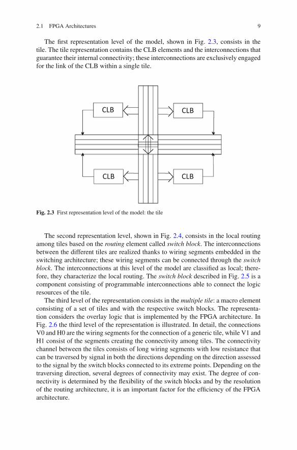
The first representation level of the model, shown in Fig. 2.3, consists in thetile. The tile representation contains the CLB elements and the interconnections thatguarantee their internal connectivity; these interconnections are exclusively engagedfor the link of the CLB within a single tile.
Fig. 2.3 First representation level of the model: the tile
The second representation level, shown in Fig. 2.4, consists in the local routingamong tiles based on the routing element called switch block. The interconnectionsbetween the different tiles are realized thanks to wiring segments embedded in theswitching architecture; these wiring segments can be connected through the switchblock. The interconnections at this level of the model are classified as local; there-fore, they characterize the local routing. The switch block described in Fig. 2.5 is acomponent consisting of programmable interconnections able to connect the logicresources of the tile.
The third level of the representation consists in the multiple tile: a macro elementconsisting of a set of tiles and with the respective switch blocks. The representa-tion considers the overlay logic that is implemented by the FPGA architecture. InFig. 2.6 the third level of the representation is illustrated. In detail, the connectionsV0 and H0 are the wiring segments for the connection of a generic tile, while V1 andH1 consist of the segments creating the connectivity among tiles. The connectivitychannel between the tiles consists of long wiring segments with low resistance thatcan be traversed by signal in both the directions depending on the direction assessedto the signal by the switch blocks connected to its extreme points. Depending on thetraversing direction, several degrees of connectivity may exist. The degree of con-nectivity is determined by the flexibility of the switch blocks and by the resolutionof the routing architecture, it is an important factor for the efficiency of the FPGAarchitecture.

10 2 Reconfigurable Field Programmable Gate Arrays: Basic Concepts
Fig. 2.4 Second representation level of the model: the local routing
Fig. 2.5 The switch-block element

2.1 FPGA Architectures 11
0
0
Fig. 2.6 The third representation level: the multiple tile
I/O I/O
I/O
I/O
I/OI/O
I/O
I/O
Fig. 2.7 The fourth representation level: the context

12 2 Reconfigurable Field Programmable Gate Arrays: Basic Concepts
The fourth level completes the representation of the FPGA context architec-ture introducing the input/output blocks dedicated to the communication with theFPGA architecture external word. The model is illustrated in Fig. 2.7 where theinput/output modules are connected to the principal FPGA interconnection, indi-cated in Fig. 2.7 as V2 and H2. The interconnections of the third and fourth levelsare classified as global and they characterize the global routing of the FPGA archi-tecture.
2.2 FPGA Configuration Technology
An FPGA architecture is composed using electrically programmable switches,where the dimensions, the capacity, and the resistance characterize the various mod-els. In this section, we describe the principal manufacturing technologies, princi-pally focusing on the volatility, reprogrammability, and complexity of the manufac-turing process.
2.2.1 Floating Gate Technology
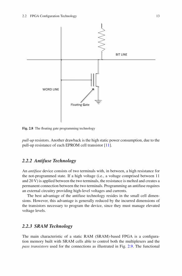
The floating gate technology is realized as an early technology based on the erasableprogrammable read only memory (EPROM) that consists of memory cells that canbe erasable using ultraviolet ray or based on the electrically erasable programmableread only memory (EEPROM) that are electrically erasable. In particular, this kindof approach is used in the model manufactured by Actel. The programmable switchillustrated in Fig. 2.8 consists of a floating-gate avalanche-injection MOS FAMOSthat can be permanently disabled by injecting a charge into the floating gate. Byapplying a high voltage difference between the gate and the drain of the FAMOStransistor, it is possible to obtain a transition of high-energy electrons from thetransistor junction to the isolated floating gate. At the end of the transition, thecharge remains indefinitely in the floating gate and the transistor remains perma-nently polarized since it does not exist an electrical connection with the gate. TheFAMOS transistor, if not programmed, is used in order to bring at low level the bitline when the word line is at high level. This approach can be further used to makeconnections between the word and the bit line; for example, it is especially usedin order to implement the wired logic functionalities such as the Wired-AND. AWired-AND logic consists in the connections of two or more wires with the supplyvoltage source through a unique resistance. The output corresponds to the productof the single signals with the same functionalities obtained using an AND gate. Forthis reason, the FAMOS transistor can be used for both the logic and the routingresources into an FPGA architecture.
The best advantage of the EPROM technology is its non-volatility. With respectto the SRAM technology, it is not requested any permanent memory outside theFPGA chip in order to store the programming data. However, the EPROM technol-ogy requires three additional manufacturing processes, in order to insert the elevated
2.2 FPGA Configuration Technology 13
Fig. 2.8 The floating gate programming technology
pull-up resistors. Another drawback is the high static power consumption, due to thepull-up resistance of each EPROM cell transistor [11].
2.2.2 Antifuse Technology
An antifuse device consists of two terminals with, in between, a high resistance forthe not-programmed state. If a high voltage (i.e., a voltage comprised between 11and 20 V) is applied between the two terminals, the resistance is melted and creates apermanent connection between the two terminals. Programming an antifuse requiresan external circuitry providing high-level voltages and currents.
The best advantage of the antifuse technology resides in the small cell dimen-sions. However, this advantage is generally reduced by the incurred dimensions ofthe transistors necessary to program the device, since they must manage elevatedvoltage levels.
2.2.3 SRAM Technology
The main characteristic of a static RAM (SRAM)-based FPGA is a configura-tion memory built with SRAM cells able to control both the multiplexers and thepass transistors used for the connections as illustrated in Fig. 2.9. The functional

14 2 Reconfigurable Field Programmable Gate Arrays: Basic Concepts
Fig. 2.9 The Static RAM configuration technology
principle is based on the logic value stored by the SRAM cell: when a logic “1” isstored, the pass transistor creates a connection between two hardwired segments;vice versa when a logic “0” is stored into the SRAM cell, the pass transistor is openand it presents a high resistance between the two hardwired segments. The state ofthe SRAM cell connected to the select line of the multiplexer illustrated in Fig. 2.9controls which input of the multiplexer is connected to the output [14].
The SRAM is volatile; therefore, the FPGA architectures using SRAM cellsrequire to be configured at each power-on. This is a relevant constraint, since itis mandatory that an SRAM-based FPGA system adopts an external and permanentmemory, like a programmable ROM (PROM), or a microprocessor-based systemthat allows to program the FPGA’s configuration memory. However, the main advan-tage of this technology is the possibility to program the device an infinite number ofcycles also in a short period.
2.3 The Logic Block
The logic blocks of the FPGA architectures, also known as configurable logic block,principally differ for their dimensions and their functional implementation capabil-ities. The difference of the several logic blocks, as in part described in the previoussections, can be classified referring to the granularity of the data. The granularitycould be defined as the number of boolean functions implemented by the logic orwith the total number of transistor. In several FPGA architectures it is difficult todistinguish between the interconnections and the logic blocks given their connectiv-ity; for simplicity we classify the FPGA model into two possible categories: logicblocks with a fine granularity, also called fine grained, and logic blocks with a coarsegranularity, or coarse grained.
2.3.1 Fine-Grain Logic Blocks
The fine-grain logic blocks consist of few interconnected elements. An exampleof a fine-grain logic block is the one manufactured by Plessey [13] as illustrated in

2.3 The Logic Block 15
Fig. 2.10 Fine-grain logic block manufactured by Plessey
Fig. 2.10. The logic is formed connecting the NAND gate to the multiplexer in orderto create the desired logic function (combinational or sequential). The SRAM cellscontrolling the configuration memory bits consist of four bits, three of them config-ure the multiplexer while the last bit is used to control the latch. For example, in casethe logic block is configured in order to implement the logic function f = ab+c, inthis case the latch is not necessary; hence, the correspondent configuration bit willbe programmed to a logic value capable to make the latch unused. The main advan-tage of the fine-grain logic block is the full usability of all the components. How-ever, nevertheless, it is easy to efficiently use few logic gates, it results drasticallydisadvantageous managing a high number of routing segments and switching ele-ments: These components generate delays and creates a huge increase in the devicesize.
2.3.2 Coarse-Grain Logic Blocks
The coarse-grain logic blocks consist of a higher number of components withrespect to the fine-grain logic blocks, principally including multiplexers, NANDgates, and LUTs. The Xilinx company is one of the top manufacturer of FPGAarchitecture embedding coarse-grain logic blocks. In Fig. 2.11 is illustrated theconfigurable logic block (CLB) of a generic Xilinx device. The basic components

16 2 Reconfigurable Field Programmable Gate Arrays: Basic Concepts
Q
COMBINATORIALFUNCTION
LOGICVARIABLES
D
RD
G
F
DINF
G
QX
QY
DINF
G
G
QY
QX
F
QD
RDENABLE CLOCK
CLOCK
DIRECTRESET
1 (ENABLE)
ABCDE
DI
EC
K
RD
Y
X
0 (INHIBIT)
(GLOBAL RESET)
CLB OUTPUTS
DATA IN0
1
0
1
MUX
MUX
Fig. 2.11 Coarse-grain logic block manufactured by Xilinx
contained in the CLB are the generator of combinational logic functions and twoD-type flip-flops whose outputs can be directly connected to the inputs of the gen-erator of combinational logic functions by using the internal routing existing in theCLB. The generator of combinational logic functions consists of two look-up tables(LUTs) with four-inputs that can be used separately or combined into a unique logicfunction. The partition of the inputs could be automatically made through a parti-tioning tool generally used during the logic synthesis or manually performed in caseparticular constraints would be implemented. On the other hand, all the sequentialcomponents have a common clock signal; besides the flip-flops that cannot be usedas latches have common signal of clock-enable and an asynchronous reset. Anyasynchronous preset can be obtained using the asynchronous reset if the data arestored in the form of active low logic level.
The principal advantage of the coarse-grain logic block is the possibility toimplement complex logic functions with few elements, reducing the need for a highnumber of programmable interconnections. However, it is difficult to obtain a highefficiency for the used resources, even if the decrease in the functional density is nota prohibitive factor.
2.4 The Routing Architecture 17
2.4 The Routing Architecture
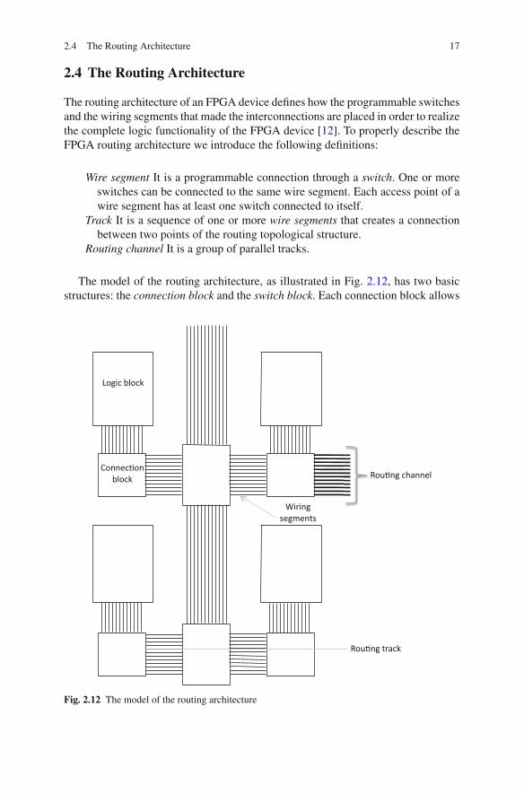
The routing architecture of an FPGA device defines how the programmable switchesand the wiring segments that made the interconnections are placed in order to realizethe complete logic functionality of the FPGA device [12]. To properly describe theFPGA routing architecture we introduce the following definitions:
Wire segment It is a programmable connection through a switch. One or moreswitches can be connected to the same wire segment. Each access point of awire segment has at least one switch connected to itself.
Track It is a sequence of one or more wire segments that creates a connectionbetween two points of the routing topological structure.
Routing channel It is a group of parallel tracks.
The model of the routing architecture, as illustrated in Fig. 2.12, has two basicstructures: the connection block and the switch block. Each connection block allows
Fig. 2.12 The model of the routing architecture


![Architecture of field-programmable gate arrays ...arantxa.ii.uam.es/~die/[Lectura FPGA Architecture] Architecture of... · Architecture of Field-Programmable Gate Arrays JONATHAN](https://img.pdfslide.us/doc/110x75/5f41b9382d13750b786f03bd/architecture-of-field-programmable-gate-arrays-dielectura-fpga-architecture.jpg)
![Field Programmable Gate Arrays [Fpga]](https://img.pdfslide.us/doc/110x75/544092dcb1af9f441d8b45c9/field-programmable-gate-arrays-fpga.jpg)