Embed Size (px)
Citation preview

Slide 1
Real Design Challenges of Low Power
Physical Design Implementation
Stefano Piccioni
Senior Design Engineer
Munich 15th May 2007

Slide 2
Welcome!
� Stefano Piccioni, Senior Design Engineer at S3
(Silicon & Software Systems)
� Worked in Accent (Milan) since 2000 before joining
S3 (Dublin) in 2005
� 8 years experience in RTL to gds2 ASIC flow
� Bachelor Degree in Physics from "Universita' degli
Studi di Bologna", Italy
� Master Degree in 'Microelectronics and Systems'
from "Universita' degli Studi di Catania", Italy

Slide 3
About S3
� The Connected Consumer Technology Company
– Enabling the delivery of next generation products and
services to the consumer, at home and on the move
� Founded in 1986
– 4 Design Centres (Ireland x 2, Czech Republic, Poland)
– 300 Employees
– Sales offices and representatives globally
� Trusted by the world's leading technology companies
– Deliver cutting-edge design solutions on time

Slide 4
� Global Leader in 90 and 65nm IC Design
– More than 30 Designs in 90nm
– Mixed Analog / Digital SoC Focus
– “First Production 65nm tapeout” - EETimes
– On schedule, right-first-time silicon
� Serving Top Tier Clients
– Including NXP, Texas Instruments
– 4 of Top 5 IDMs and 3 of Top 5 Fabless
� Teaming with Leading Technology Partners
– Including TSMC, IBM, Cadence, ARM, UMC
About S3

Slide 5
Presentation Overview
� Low power techniques
� Testcase Introduction
� Design Challenges
� Conclusions

Slide 6
� With new mobile devices power consumption has become an hot topic
� New handsets are very complex devices and need high performance
together with low power consumption
� Battery life represents an important feature in choosing a product in the
market but has not been improved as expected by modern technologies
� That’s the reason why is important to minimize device power consumption
using new design techniques
Low Power Techniques - Overview

Slide 7
� Different low power techniques can be applied throughout the design
cycle, from architectural level down to physical implementation
� EDA vendors together with silicon vendors offer a wide range of design
solutions and libraries targeted to low power
� Power consumption concurrently optimized together with Area and Timing
� Principal Low Power Techniques are
– Clock Gating and Operand Isolation
– Leakage Optimization and use of Multi VT Libraries
– MSMV with automatic insertion of level shifters
Low Power Techniques - Overview

Slide 8
• Power consumption is a sum of
Dynamic + Static contributors
• Dynamic power consumption
(power consumed during state changes)
� Internal power dissipation, which includes switching of the transistors inside the
cell and the power dissipated when charging or discharging internal net
capacitances
� Net power includes switching power consumed by charging and discharging the
chip wires capacitance
• Static power consumption
(power statically dissipated)
� Leakage power dissipation of the cell,
With today’s technology shrinking down
to 90 nm and below, the leakage power
becomes more and more dominant.
Low Power Techniques – Power Consumption

Slide 9
•Even if data is loaded into registers very infrequently in most designs,
the clock signal continues to toggle at every clock cycle
•Gating a group of flip-flops that are enabled by the same control
signal reduces unnecessary clock toggles
• In the idle period power is saved in the gated-clock circuitry
(tipically portion of clock tree and registers)
Low Power Techniques – Clock Gating

Slide 10
• Operand Isolation is a dynamic power optimization technique that can
reduce power dissipation in datapath blocks controlled by an enable signal.
• Its main purpose is to shutdown (isolate) the function unit (operand)
when its results are not used
•Example: When the Enable is off, register C only uses the result of register B, but
the multiplier continues its computations. Because the multiplier dissipates the most
power, the total amount of power wasted is quite significant.
Low Power Techniques – Operand Isolation

Slide 11
• Consist mainly in using different libraries with different voltage
thresholds (typically LowVT and HighVT) in order to reduce leakage
power consumption:
• LVT cells are faster but dissipate more leakage power
• HVT cells are slower but dissipate less leakage power
• Different synthesis approaches can be used
• Physical implementation is performed mostly using HVT,
limiting LVT cells only where it is not possible to close timing
• After final routing, an usual IPO consists in replacing LVT cells
with HVT cells with same footprint, so no re-routing is required
Low Power Techniques – Leakage Optimization

Slide 12
• It is possible to use in the same design different voltage islands that
can be switched on/off individually or supplied with different voltages
• Dynamically switching off entire modules when not used has a bigger
impact on power savings because all leakage power consumption
completely disappears
• The need to accommodate multiple power domains and multiple voltage
levels makes low-power chip design much more complex
• MSMV capable tools are needed to assist the designer at every step of
the flow
Low Power Techniques – MSMV

Slide 13
� A typical MSMV flow involves:
� Floorplanning and power domains definitions
� Insertion of level shifters (and isolation cells) at RTL or netlist level
� Placement of level shifters (and isolation cells) in correct power domain
and additional followpin connections
� MSMV and power aware optimization
� Clock tree insertion that takes into account different domains and low
power techniques
� Power analysis and Irdrop run on different grids
� DRC / LVS check and formal verification considering different voltage
supplies
Low Power Techniques – MSMV

Slide 14
Level Shifters additional
power pin connection
Floor-planning and
Power Domains creation
Level Shifters
placement
Clock Tree
insertion with
MSMV
Low Power Techniques – MSMV Examples

Slide 15
� Overview
� Design Tasks
� Power Domains
� Isolation Cell Handling
� Power Switch Handling
� Power Grid Design
� Power Estimation and Analysis
� Physical Verification
Test Case Introduction

Slide 16
� Technology:
– 90nm
– 6 metal layers
� Target Die Area:
– 21sq.mm
– ~1Mgates
� Power Domains:
– Several gated PD
– 1 always on
� Target IR drop:
– 10% (5%vdd+5%vss)
� Priority:
– Area
– Power
– Performance
Test Case Overview

Slide 17
Design Tasks
� Synthesis (RC)
– High-Vt library only
� Floorplanning (SoCE)
– IO planning
– Power domains grid planning
� P&R (SoCE)
– Isolation cell placement
– Power domain aware CTS/opt.
– Power domain crossing checks (S3 script)
– Power domain aware filler insertion (H/L Leakage decap)
– Allow standard-Vt library for manual fixes (not in AO PD)
� STA/SI (F&I/PT-SI/CeltIC)
� PV/FV (Calibre/Conformal)
� Power/IRDrop Analysis (Powermeter/Vstorm)

Slide 18
Power Domains
� Power management domain is ‘always
on’ and is defined as default power
domain
� Multiple independently power
switchable domains
� High connectivity between ‘always on’
and other domains created high
placement density near domains
boundaries
� Choosing the domain shapes that
minimize congestion took a
considerable amount of time and
resulted in very irregular shapes

Slide 19
Isolation Cells
� Isolation cells have been inserted on all nets crossing gated power domains to the ‘ always-on’ domain (>1000)
############################ Specify Isolation Cells ############################specifyIsolationCell -cell {ISO_OR2_8} specifyIsolationCell -cell {ISO_NR2B_8} specifyIsolationCell -cell {ISO_AN2_8}
• It has been checked that iso cells have been correctly recognized using:
reportIsolation -outfile isolationcells.rpt
• Then we placed them together with all the logic and then highlight them with:
reportIsolation -highlight
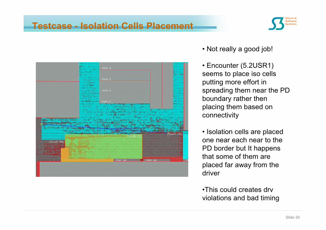
Slide 20
• Not really a good job!
• Encounter (5.2USR1)
seems to place iso cells
putting more effort in
spreading them near the PD
boundary rather then
placing them based on
connectivity
• Isolation cells are placed
one near each near to the
PD border but It happens
that some of them are
placed far away from the
driver
•This could creates drv
violations and bad timing
Testcase - Isolation Cells Placement
Slide 21
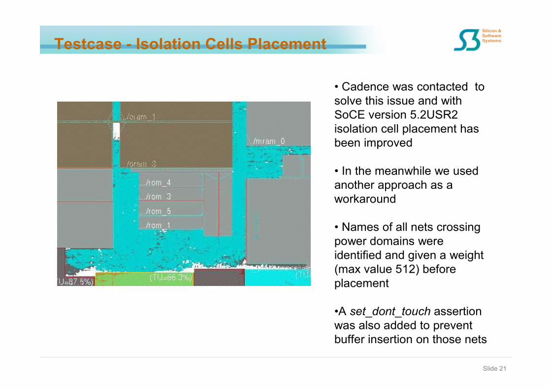
• Cadence was contacted to
solve this issue and with
SoCE version 5.2USR2
isolation cell placement has
been improved
• In the meanwhile we used
another approach as a
workaround
• Names of all nets crossing
power domains were
identified and given a weight
(max value 512) before
placement
•A set_dont_touch assertion
was also added to prevent
buffer insertion on those nets
Testcase - Isolation Cells Placement

Slide 22
• As a result isolation
cells placement was more
‘connection’ driven
• Now length of all nets is
minimized through placement of
isolation cells as close as
possible to the logic they talk to
Testcase - Isolation Cells Placement
Slide 23
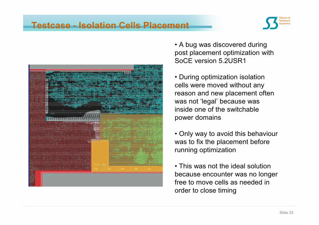
• A bug was discovered during
post placement optimization with
SoCE version 5.2USR1
• During optimization isolation
cells were moved without any
reason and new placement often
was not ‘legal’ because was
inside one of the switchable
power domains
• Only way to avoid this behaviour
was to fix the placement before
running optimization
• This was not the ideal solution
because encounter was no longer
free to move cells as needed in
order to close timing
Testcase - Isolation Cells Placement

Slide 24
• Cadence was contacted in order to
fix this bug and they discovered a
problem with ‘refinePlacement’
(placement legalization) during
optimization and fixed it
• Cadence sent us a pre-release
version of Encounter that solved the
issue and let us tape out in time
• Also this problem was definitely
solved with SoCE version 5.2USR2
Testcase - Isolation Cells Placement

Slide 25
Power Switches
� On-chip voltage regulator
� Power switches (nr)
– 2ohm resistance (rs)
– Max 5% IR drop (p)
– nr >= (k * ng * c * f * rs)/ p
� Cascaded switching
– switch_ready asserted 2us
after switch enable to slowly
turn on power switches
minimizing voltage drop
sw_outsw_outsw_insw_in
sw_enbsw_enbsw_rdysw_rdy
SwitchSwitch
sw_outsw_outsw_insw_in
sw_enbsw_enbsw_rdysw_rdy
SwitchSwitch

Slide 26
� Power switches layout guidelines
– Max 30mA output requirement
– Use of M3-M6 metal layers
VDD_CORELOGICVDD_CORELOGIC
VDD_PDVDD_PD
sw_insw_in
sw_outsw_out
Power Switches

Slide 27
Power Grid
� Power island grids
� Regulator – pads grid
� Power switches
connection
� Core grid
– Incl. always-on island
� IO ring
� RAMs grids / rings
� Analog macro hook-up

Slide 28
Power Grid
� Regulator – power pads
– 120mA requirement
– Use of all metal layers
• M6 1.5mA/um
• M2-M5 1.0mA/um
• M1 0.6mA/um
VOUT VSS VIN VSS_53 VOUT_53 VIN_53VOUT VSS VIN VSS_53 VOUT_53 VIN_53

Slide 29
Power Grid
� IO, Rams and core grids

Slide 30
Power Measurement and Analysis
� Power measurement
– Powermeter upgraded to
cadence_anls 6.1
– Now fully power aware
– ~200mW consumption
� Power analysis
– Vstorm updated to
cadence_anls 6.1
– Supports analysis through
power switches
– Multiple power-gate dependent
runs
– IR drop requirements met after
iterations

Slide 31
Physical Verification
� DRC - Max Density
– Trade-off between density and
power ring-width requirements
� LVS
– Text points for power domains

Slide 32
Conclusions
� Low power techniques permeate every step in implementation flow
� MSMV involves a more complex flow with additional resources required and possible impact on schedule
� ‘Young’ features, designer need to work closer to EDA vendor
� Routing congestion could get worse due to power islands
� Timing closure more difficult with level shifters
� New type of possible errors, new type of checks
� Better equipped for low power implementation

Slide 33
Thank you!
� QUESTION?

![Physical-chemical gas-dynamics: challenges andsolutionsjnaiam.org/uploads/Volume9-10_Issues_1-2_Part_III.pdf · Physical-chemical gas-dynamics: challenges and solutions 23 generalapproach[10,11])](https://img.pdfslide.us/doc/110x75/5b5acabb7f8b9a01748ca568/physical-chemical-gas-dynamics-challenges-physical-chemical-gas-dynamics-challenges.jpg)