Embed Size (px)
Citation preview
PROGRESS IN PHOTOVOLTAICS: RESEARCH AND APPLICATIONSProg. Photovolt: Res. Appl. (2012)
Published online in Wiley Online Library (wileyonlinelibrary.com). DOI: 10.1002/pip.2186
RESEARCH ARTICLE
Reflectiondistributionsof texturedmonocrystalline silicon:implications for silicon solar cellsSimeon C. Baker-Finch1* and Keith R. McIntosh2
1 College of Engineering and Computer Science, Australian National University, Canberra, ACT 0200, Australia2 PV Lighthouse, Coledale, NSW 2515, Australia
ABSTRACT
A common misconception is that alkaline textured silicon solar cell surfaces are characterised by features that are pyramidaland bounded by {111} planes. In preference to the typical approach of observing scanning electron microscope images, weanalyse reflection distributions from various pyramidal textures and find that {111} faceted pyramids are a poor approxi-mation to the features on such surfaces. We conclude that features are hillocks, with an octagonal base. Furthermore, thecharacteristic base angle of the texture depends on the etchant and is closer to 50–52� than the commonly accepted valueof 54.74�. Analyses of antireflection, light trapping, photogeneration and surface recombination properties of texturedsurfaces should take this feature morphology into account. The base angle has a strong influence on the hemisphericalreflectance of the textured surface, with higher angles resulting in reduced reflectance. The influence of this reflectionenhancement upon device performance is smallest when an optimised antireflection coating is applied; compared withan array of {111} faceted pyramids, a hillock morphology with 50� base angle results in a 0.2% reduction in photogeneratedcurrent in a typical cell. Additionally, as base angle is reduced, an encapsulant of increasingly higher refractive index is requiredto drive internal reflection at the air–glass interface of light initially reflected from the cell surface. The development of texturingprocesses resulting in higher base angles is encouraged. Copyright © 2012 John Wiley & Sons, Ltd.
KEYWORDS
texture; reflection distribution; optics; ray tracing; antireflection coating
*Correspondence
Simeon C. Baker-Finch, College of Engineering and Computer Science, Australian National University, Canberra, ACT 0200, Australia.E-mail: [email protected]
Received 21 October 2011; Revised 13 December 2011; Accepted 10 February 2012
1. INTRODUCTION
The sunward surface of a silicon solar cell is almost alwaystextured. When the surface is rough, rather than planar,light is more effectively coupled into, and retained inside,the active region of such a device. Monocrystalline siliconwafers are most commonly processed in an alkaline textur-ing solution that is intended to produce a random array ofupright pyramids on the etched surface. It is the anisotropicnature of such an etchant (where the etch rate in the<100> direction is several times greater than that in the<111> direction) that drives the formation of a repeatedpyramidal or hillock feature. Many and varied etchantshave been investigated, including aqueous solutions ofNaOH [1,2], Na2CO3 [3–5], KOH [6] and TMAH [7,8];the success or otherwise of the process tends to dependon temperature and composition of the solution (the addi-tion of isopropyl alcohol (IPA) is often critical) as well asthe pre-etch properties of the silicon surface. The final mor-phology of the features has various implications for the
Copyright © 2012 John Wiley & Sons, Ltd.
performance of silicon solar cells; front-surface reflec-tance, light trapping capacity, module performance andsurface recombination may all be affected.
Typically, scanning electron microscope images of thevariety depicted in Figure 1 are used to assess texturedsilicon (see, e.g. [2,9]). Such images are usually providedas evidence that the texture consists of ideal {111} facetedupright pyramids. More careful examination of the featuresusually suggests otherwise [10,11]. Indeed, in fields ofmicromachining, texture features have been studied exten-sively [10–14]. However, relatively few conclusions havebeen transferred into the analysis of surface texture in siliconsolar cell applications. What is generally, and often errantly,assumed to be a texture consisting of upright tetrahedral fea-tures bounded by {111} planes (i.e. square-based pyramids,as shown at the left in Figure 2(a)) is probably an assortmentof so-called ‘hillocks’ [10,13,14]. Depending on the etchingconditions, the hillocks range from near-perfect uprightpyramids with some slight bowing of the facets or bevellingof edges [12] to features with distinctly octagonal (rather
Figure 1. Scanning electron microscope images of silicon textured in alkaline solution, taken at 45� tilt. The sample at the left istextured in a TMAH solution, and the sample at the right is textured in a KOH solution. The images depict the samples used in the
experimental work outlined in Section 3.
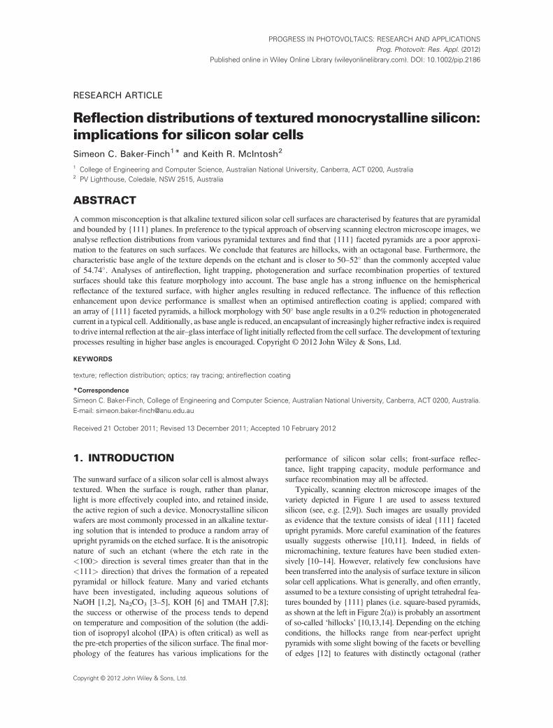
Figure 2. (a) A representation of a near {111} faceted pyramid (left) and a hillock, with octagonal base (right). (b) Dominant paths ofreflection at pyramidal texture, after [20]. (c) The characteristic base angle a of a pyramid or hillock is defined as the inclination of
the facets with respect to the <100> oriented base.
Reflection distributions of textured monocrystalline silicon S. C. Baker-Finch and K. R. McIntosh
than quadrilateral) bases [10] of the kind illustrated at theright in Figure 2(a). The precise mechanism for the develop-ment of such hillocks remains contentious; two likely contri-butors are as follows: (i) the exposure of a convex corner ofthe growing feature results in the etching of higher index‘bevelling’ planes that eventually intersect to form a stablebowed facet; and (ii) the formation of kinks or ledges(terrace-like structures—see the bottom right corner of theleftmost image in Figure 1 for an example) on the pyramidfacet as etching proceeds [10–14].
Additionally, the angle between the macroscopic sur-face and each plane of the hillock or pyramid (defined inFigure 2(c) and referred to hereafter as the base angle a)is usually less than the angle that would be observed for
ideal {111} bounded pyramids (i.e. arctanffiffiffi2
p= 54.74�).
Typical industrial cells may have a between 49� and 53�
[15,16], but certain etchants may result in ‘flatter’ features,with a as low as 45� [13]. As we discuss in detail in thefollowing text, a is particularly critical to the modellingand performance of the textured solar cell surface.
Texture morphology has a decisive impact on the anti-reflective capacity of the sunward surface of the cell, aswell as implications in antireflection coating (ARC) opti-misation and light trapping. Furthermore, a determinesthe extent to which reflected light is given a second chanceto be absorbed by the cell when encapsulated (following
internal reflection at the glass–air boundary). As well, itis likely that minor variations in morphology influence sur-face recombination and passivation. Given that the texturemorphology evolves as the composition of an etch bathchanges, a method for characterisation of the evolvingmorphology is a critical precursor to precise process con-trol. One such method is developed in this paper. Further-more, a more accurate geometric model of the surface,derived from the application of this method, offers a guidefor the improvement of current optical models of thetextured silicon surface.
The analysis of the reflection distribution of textured sili-con has been suggested as a means of assessing the ability ofthe surface morphology to contribute positively to the effi-ciency of a completed solar cell device [15,17–19]. Usually,themeasurement apparatus includes a laser aligned to the sam-ple normal and a photosensitive screen [15] or an array ofphotodiodes [16] for capturing the reflected radiation. Theapproach of Fornies et al. [15] is to determine a figure of meritthat represents the proportion of flat areas on the sample,where texturing has not occurred. This figure of merit issimply equal to the ratio of the light reflected along ‘A’ paths(Figure 2(b)) to the light reflected normal to the sample. Theapproach is well suited to inline assessment of texture quality,but further analysis of the reflection distribution offers animproved understanding of the texture morphology.
Prog. Photovolt: Res. Appl. (2012) © 2012 John Wiley & Sons, Ltd.DOI: 10.1002/pip
Reflection distributions of textured monocrystalline siliconS. C. Baker-Finch and K. R. McIntosh
In this work, we present a methodology for the quantita-tive measurement of the reflection distribution of texturedsilicon. In particular, we employ a spectrophotometer withan angular reflectance accessory to determine such distribu-tions for silicon samples featuring either a regular array ofinverted pyramids having {111} facets or a random arrayof pyramidal or near pyramidal features. The measurementis sufficiently sensitive to detect the reflectance from both‘A’ and ‘C’ paths (Figure 2(b) or [20] for more detail) frominverted pyramid texture. Critically, we find this techniqueto provide direct access to the morphology of the texturefeatures; unlike the scanning electron microscope imageanalysis approach, the assessment of optical reflectiondistributions is sensitive to the presence of hillocks and tolower-than-ideal values of a.
Reflection distributions emerging from random texturesuggest that a commonly used geometric approximation(namely that texture features are tetrahedral, with {111}facets) is flawed in two ways: (i) the angle between the fea-ture base and facets is significantly less than expected; and(ii) the base of each feature is not square, but octagonal, sothat there are eight (rather than four) facets of each feature,and these features have a combination of orientations (andthat these orientations are higher index planes, not {111}).
The implications of these findings for the optical analy-sis of silicon solar cells are manifold: (i) the antireflectionand light trapping action of the texture is determined byits precise morphology; (ii) the capture of reflected lightin the module in which the cell is encapsulated dependson the angular distribution of reflection; and (iii) flatterfeatures may potentially be better passivated than sharperones. The accurate characterisation of textured silicontends to depend on a reasonable approximation of the frontsurface texture geometry.
2. VARIABLE ANGLESPECTROPHOTOMETRY FORASSESSMENT OF SILICON SOLARCELL TEXTURE
2.1. Theory and experimental apparatus
Variable angle spectrophotometry is a technique that typi-cally complements or replaces spectroscopic ellipsometryas a means for determining the thickness and refractiveindex of thin films [21]. The experimental apparatus,specifically a spectrophotometer equipped with motorisedstages (goniometers), allows sample and detector anglesto be varied with a high degree of accuracy [22]. Variablesample and detector angles render the apparatus capable ofa broad range of measurements including those of angularresolved scattering and bidirectional reflectance/transmit-tance distribution functions.
In this work, we employed a Perkin Elmer Lambda 1050spectrophotometer along with an Absolute Reflectance/Transmittance Analyser accessory from OMT Solutions(Eindhoven, The Netherlands) [21]. The experimental layout
Prog. Photovolt: Res. Appl. (2012) © 2012 John Wiley & Sons, Ltd.DOI: 10.1002/pip
is illustrated in Figure 3(a). An integrating sphere of 65-mmdiameter served as detector of the normally incident,polarised light that is reflected from the sample with angleθr�od to the macroscopic normal of the sample surface.For the measurements undertaken in this work, the detectoropening width od = 0.25�, meaning that measurements ofreflectance R as a function of θr represent the integratedreflectance in a 0.5� wide slice of the reflection distributionfunction. As illustrated in the isometric representation ofthe apparatus in Figure 3(b), the zenith anglefr was adjustedby rotation of the sample about the incoming beam path; wedefine fr = 0 when the <110> flat, the incoming beam andthe detector are coplanar. The detector opening correspondsto �7.5� resolution in fr. In total, the detector openingsubtends a solid angle of ~0.002 steradians of the reflectancesphere.
Note that the incident beam is not collimated; rather, asshown in Figure 3(c), it is focused so as to obtain an imageof the monochromators slit on the sample surface. A widerbeam (in which the energy is distributed over approximately10�) is hence found at the entrance to the integrating sphere.As is shown in Figure 3(c) and (d), the non-collimation of thebeam at the sample results in a broader beam divergence atthe detector. We used an inverted pyramid textured siliconwafer as a means or correcting for this divergence; atechnique for doing so is described in the following text.
Rays normally incident to a textured surface aretypically reflected along a number of discrete paths [20].The proportion of the incident radiation reflected at a par-ticular θr and fr depends on the proportion of rays reflectedalong a certain path, as well as the reflectance of that path.With a collimated beam, we would therefore expect tomeasure distinct delta function peaks in the reflectiondistribution functions at pairs (θj, fj), where j representsone particular path (A thru G in [20]).
The sensitivity of our measurements (~0.01% of theincident radiation) limits us to the observation of pathshaving at least moderate reflectance and, most importantly,a high ‘path fraction’ (usually paths A and C). We measuredthe reflection distribution function with incident radiationhaving a 270-nm wavelength. Advantageously, this wave-length is well below the texture feature size, thus renderingdiffractive effects negligible (perhaps with the exception ofdiffraction at sharp peaks or troughs). As evidenced in thefollowing text, the reflectance signal at this wavelength wassufficiently high that noise did not adversely impact uponour measurements.
2.2. Reflection distribution from regularinverted pyramids
We probed a sample having known surface morphology,namely a regular array of inverted pyramids, to validatethe experimental setup. In the following, we find closeagreement between experiment and a reflection distributiondetermined by ray tracing. Additionally, the measurementof a known structure allows us to quantify the impacts ofthe non-collimation of the incident beam.
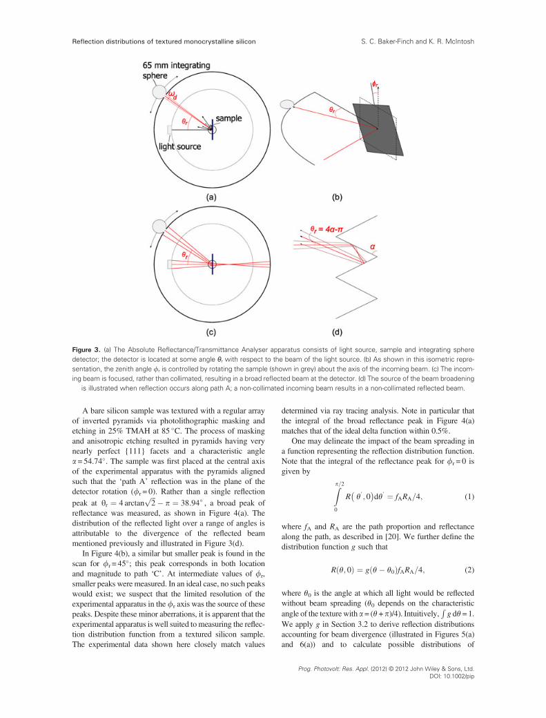
Figure 3. (a) The Absolute Reflectance/Transmittance Analyser apparatus consists of light source, sample and integrating spheredetector; the detector is located at some angle θr with respect to the beam of the light source. (b) As shown in this isometric repre-sentation, the zenith angle fr is controlled by rotating the sample (shown in grey) about the axis of the incoming beam. (c) The incom-ing beam is focused, rather than collimated, resulting in a broad reflected beam at the detector. (d) The source of the beam broadening
is illustrated when reflection occurs along path A; a non-collimated incoming beam results in a non-collimated reflected beam.
Reflection distributions of textured monocrystalline silicon S. C. Baker-Finch and K. R. McIntosh
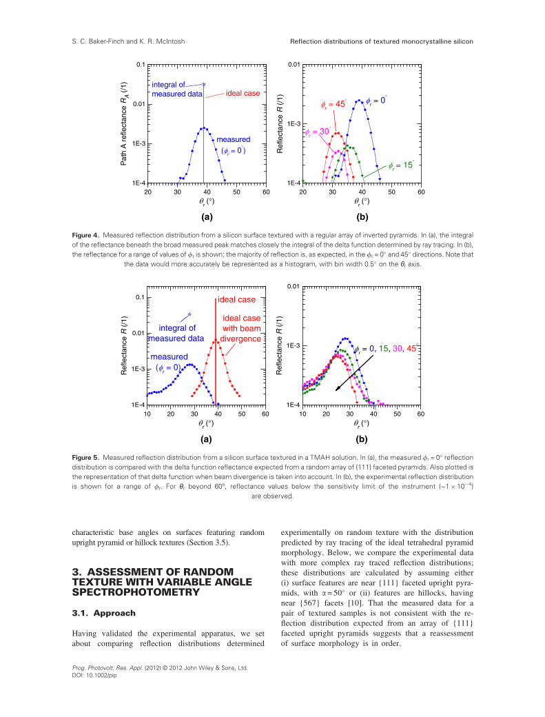
A bare silicon sample was textured with a regular arrayof inverted pyramids via photolithographic masking andetching in 25% TMAH at 85 �C. The process of maskingand anisotropic etching resulted in pyramids having verynearly perfect {111} facets and a characteristic anglea= 54.74�. The sample was first placed at the central axisof the experimental apparatus with the pyramids alignedsuch that the ‘path A’ reflection was in the plane of thedetector rotation (fr = 0). Rather than a single reflection
peak at θr ¼ 4 arctanffiffiffi2
p � p ¼ 38:94∘ , a broad peak ofreflectance was measured, as shown in Figure 4(a). Thedistribution of the reflected light over a range of angles isattributable to the divergence of the reflected beammentioned previously and illustrated in Figure 3(d).
In Figure 4(b), a similar but smaller peak is found in thescan for fr = 45�; this peak corresponds in both locationand magnitude to path ‘C’. At intermediate values of fr,smaller peaks were measured. In an ideal case, no such peakswould exist; we suspect that the limited resolution of theexperimental apparatus in the fr axis was the source of thesepeaks. Despite these minor aberrations, it is apparent that theexperimental apparatus is well suited to measuring the reflec-tion distribution function from a textured silicon sample.The experimental data shown here closely match values
determined via ray tracing analysis. Note in particular thatthe integral of the broad reflectance peak in Figure 4(a)matches that of the ideal delta function within 0.5%.
One may delineate the impact of the beam spreading ina function representing the reflection distribution function.Note that the integral of the reflectance peak for fr = 0 isgiven by
Zp=2
0
R θ′; 0� �
dθ′ ¼ fARA=4; (1)
where fA and RA are the path proportion and reflectancealong the path, as described in [20]. We further define thedistribution function g such that
R θ; 0ð Þ ¼ g θ� θ0ð ÞfARA=4; (2)
where θ0 is the angle at which all light would be reflectedwithout beam spreading (θ0 depends on the characteristicangle of the texture with a= (θ+p)/4). Intuitively,
Rg dθ=1.
We apply g in Section 3.2 to derive reflection distributionsaccounting for beam divergence (illustrated in Figures 5(a)and 6(a)) and to calculate possible distributions of
Prog. Photovolt: Res. Appl. (2012) © 2012 John Wiley & Sons, Ltd.DOI: 10.1002/pip
1E-4
1E-3
0.01
20 30 40 50 6020 30 40 50 601E-4
1E-3
0.01
0.1
(b)
Ref
lect
ance
R (
/1)
r( )
(a)
integral ofmeasured data
measured
Pat
h A
ref
lect
ance
RA (
/1)
r( )
ideal case
Figure 4. Measured reflection distribution from a silicon surface textured with a regular array of inverted pyramids. In (a), the integralof the reflectance beneath the broad measured peak matches closely the integral of the delta function determined by ray tracing. In (b),the reflectance for a range of values of fr is shown; the majority of reflection is, as expected, in the fr = 0� and 45� directions. Note that
the data would more accurately be represented as a histogram, with bin width 0.5� on the θr axis.
1E-4
1E-3
0.01
10 20 30 40 50 6010 20 30 40 50 601E-4
1E-3
0.01
0.1
Ref
lect
ance
R (
/1)
r( )
ideal case
integral ofmeasured data
measured
(a) (b)
Ref
lect
ance
R (
/1)
r( )
ideal casewith beam
divergence
Figure 5. Measured reflection distribution from a silicon surface textured in a TMAH solution. In (a), the measured fr = 0� reflectiondistribution is compared with the delta function reflectance expected from a random array of {111} faceted pyramids. Also plotted isthe representation of that delta function when beam divergence is taken into account. In (b), the experimental reflection distributionis shown for a range of fr. For θr beyond 60º, reflectance values below the sensitivity limit of the instrument (~1� 10�4)
are observed.
Reflection distributions of textured monocrystalline siliconS. C. Baker-Finch and K. R. McIntosh
characteristic base angles on surfaces featuring randomupright pyramid or hillock textures (Section 3.5).
3. ASSESSMENT OF RANDOMTEXTURE WITH VARIABLE ANGLESPECTROPHOTOMETRY
3.1. Approach
Having validated the experimental apparatus, we setabout comparing reflection distributions determined
Prog. Photovolt: Res. Appl. (2012) © 2012 John Wiley & Sons, Ltd.DOI: 10.1002/pip
experimentally on random texture with the distributionpredicted by ray tracing of the ideal tetrahedral pyramidmorphology. Below, we compare the experimental datawith more complex ray traced reflection distributions;these distributions are calculated by assuming either(i) surface features are near {111} faceted upright pyra-mids, with a= 50� or (ii) features are hillocks, havingnear {567} facets [10]. That the measured data for apair of textured samples is not consistent with the re-flection distribution expected from an array of {111}faceted upright pyramids suggests that a reassessmentof surface morphology is in order.
1E-4
1E-3
0.01
0.1
10 20 30 40 50 60 10 20 30 40 50 601E-4
1E-3
0.01
ideal casewith beam
divergence R
efle
ctan
ce R
(/1
)
r( )
(b)(a)
Ref
lect
ance
R (
/1)
r( )
ideal case
integral ofmeasured data
measured
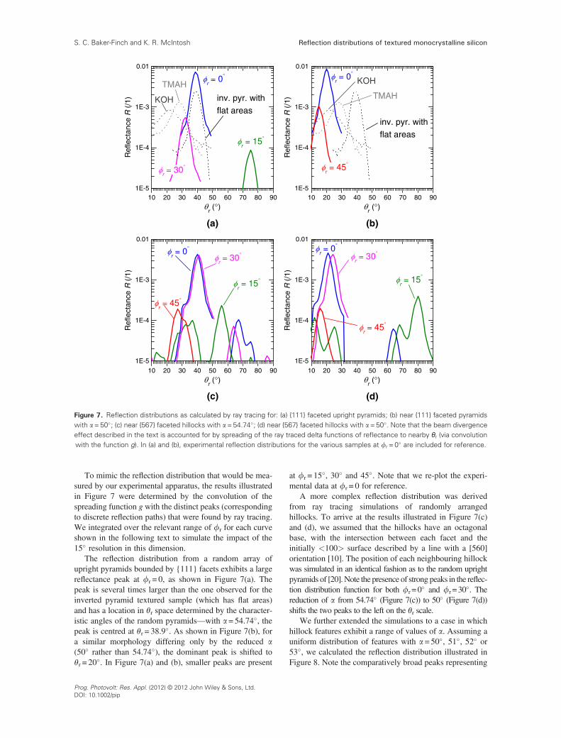
Figure 6. Measured reflection distribution from a silicon surface textured in a KOH solution. Details are the same as for Figure 5.
Reflection distributions of textured monocrystalline silicon S. C. Baker-Finch and K. R. McIntosh
3.2. Measured reflection distributionfunctions
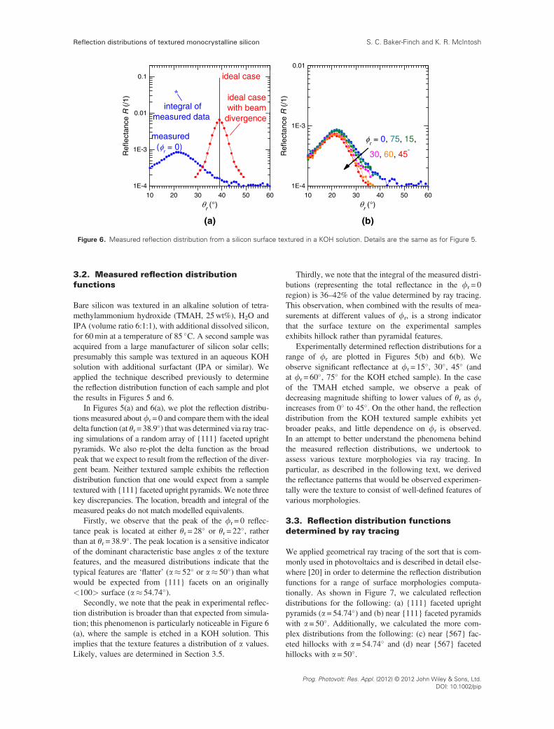
Bare silicon was textured in an alkaline solution of tetra-methylammonium hydroxide (TMAH, 25wt%), H2O andIPA (volume ratio 6:1:1), with additional dissolved silicon,for 60min at a temperature of 85 �C. A second sample wasacquired from a large manufacturer of silicon solar cells;presumably this sample was textured in an aqueous KOHsolution with additional surfactant (IPA or similar). Weapplied the technique described previously to determinethe reflection distribution function of each sample and plotthe results in Figures 5 and 6.
In Figures 5(a) and 6(a), we plot the reflection distribu-tions measured about fr = 0 and compare themwith the idealdelta function (at θr = 38.9�) that was determined via ray trac-ing simulations of a random array of {111} faceted uprightpyramids. We also re-plot the delta function as the broadpeak that we expect to result from the reflection of the diver-gent beam. Neither textured sample exhibits the reflectiondistribution function that one would expect from a sampletextured with {111} faceted upright pyramids. We note threekey discrepancies. The location, breadth and integral of themeasured peaks do not match modelled equivalents.
Firstly, we observe that the peak of the fr = 0 reflec-tance peak is located at either θr = 28� or θr = 22�, ratherthan at θr = 38.9�. The peak location is a sensitive indicatorof the dominant characteristic base angles a of the texturefeatures, and the measured distributions indicate that thetypical features are ‘flatter’ (a� 52� or a� 50�) than whatwould be expected from {111} facets on an originally<100> surface (a� 54.74�).
Secondly, we note that the peak in experimental reflec-tion distribution is broader than that expected from simula-tion; this phenomenon is particularly noticeable in Figure 6(a), where the sample is etched in a KOH solution. Thisimplies that the texture features a distribution of a values.Likely, values are determined in Section 3.5.
Thirdly, we note that the integral of the measured distri-butions (representing the total reflectance in the fr = 0region) is 36–42% of the value determined by ray tracing.This observation, when combined with the results of mea-surements at different values of fr, is a strong indicatorthat the surface texture on the experimental samplesexhibits hillock rather than pyramidal features.
Experimentally determined reflection distributions for arange of fr are plotted in Figures 5(b) and 6(b). Weobserve significant reflectance at fr = 15�, 30�, 45� (andat fr = 60�, 75� for the KOH etched sample). In the caseof the TMAH etched sample, we observe a peak ofdecreasing magnitude shifting to lower values of θr as fr
increases from 0� to 45�. On the other hand, the reflectiondistribution from the KOH textured sample exhibits yetbroader peaks, and little dependence on fr is observed.In an attempt to better understand the phenomena behindthe measured reflection distributions, we undertook toassess various texture morphologies via ray tracing. Inparticular, as described in the following text, we derivedthe reflectance patterns that would be observed experimen-tally were the texture to consist of well-defined features ofvarious morphologies.
3.3. Reflection distribution functionsdetermined by ray tracing
We applied geometrical ray tracing of the sort that is com-monly used in photovoltaics and is described in detail else-where [20] in order to determine the reflection distributionfunctions for a range of surface morphologies computa-tionally. As shown in Figure 7, we calculated reflectiondistributions for the following: (a) {111} faceted uprightpyramids (a= 54.74�) and (b) near {111} faceted pyramidswith a= 50�. Additionally, we calculated the more com-plex distributions from the following: (c) near {567} fac-eted hillocks with a= 54.74� and (d) near {567} facetedhillocks with a= 50�.
Prog. Photovolt: Res. Appl. (2012) © 2012 John Wiley & Sons, Ltd.DOI: 10.1002/pip
1E-5
1E-4
1E-3
0.01
1E-5
1E-4
1E-3
0.01
1E-5
1E-4
1E-3
0.01
20 30 40 50 60 70 80 90 1010 20 30 40 50 60 70 80 90
10 20 30 40 50 60 70 80 90 10 20 30 40 50 60 70 80 90
1E-5
1E-4
1E-3
0.01
KOH
TMAH
inv. pyr. withflat areas
(d)(c)
(a)
Ref
lect
ance
R (
/1)
r( )
Ref
lect
ance
R (
/1)
r( )
inv. pyr. withflat areas
TMAH
KOH
Ref
lect
ance
R (
/1)
r( )
(b)
Ref
lect
ance
R (
/1)
r( )
Figure 7. Reflection distributions as calculated by ray tracing for: (a) {111} faceted upright pyramids; (b) near {111} faceted pyramidswith a=50�; (c) near {567} faceted hillocks with a=54.74�; (d) near {567} faceted hillocks with a=50�. Note that the beam divergenceeffect described in the text is accounted for by spreading of the ray traced delta functions of reflectance to nearby θr (via convolutionwith the function g). In (a) and (b), experimental reflection distributions for the various samples at fr = 0� are included for reference.
Reflection distributions of textured monocrystalline siliconS. C. Baker-Finch and K. R. McIntosh
To mimic the reflection distribution that would be mea-sured by our experimental apparatus, the results illustratedin Figure 7 were determined by the convolution of thespreading function g with the distinct peaks (correspondingto discrete reflection paths) that were found by ray tracing.We integrated over the relevant range of fr for each curveshown in the following text to simulate the impact of the15� resolution in this dimension.
The reflection distribution from a random array ofupright pyramids bounded by {111} facets exhibits a largereflectance peak at fr = 0, as shown in Figure 7(a). Thepeak is several times larger than the one observed for theinverted pyramid textured sample (which has flat areas)and has a location in θr space determined by the character-istic angles of the random pyramids—with a= 54.74�, thepeak is centred at θr = 38.9�. As shown in Figure 7(b), fora similar morphology differing only by the reduced a(50� rather than 54.74�), the dominant peak is shifted toθr = 20�. In Figure 7(a) and (b), smaller peaks are present
Prog. Photovolt: Res. Appl. (2012) © 2012 John Wiley & Sons, Ltd.DOI: 10.1002/pip
at fr = 15�, 30� and 45�. Note that we re-plot the experi-mental data at fr = 0 for reference.
A more complex reflection distribution was derivedfrom ray tracing simulations of randomly arrangedhillocks. To arrive at the results illustrated in Figure 7(c)and (d), we assumed that the hillocks have an octagonalbase, with the intersection between each facet and theinitially <100> surface described by a line with a [560]orientation [10]. The position of each neighbouring hillockwas simulated in an identical fashion as to the random uprightpyramids of [20].Note the presence of strong peaks in the reflec-tion distribution function for both fr = 0� and fr = 30�. Thereduction of a from 54.74� (Figure 7(c)) to 50� (Figure 7(d))shifts the two peaks to the left on the θr scale.
We further extended the simulations to a case in whichhillock features exhibit a range of values of a. Assuming auniform distribution of features with a= 50�, 51�, 52� or53�, we calculated the reflection distribution illustrated inFigure 8. Note the comparatively broad peaks representing
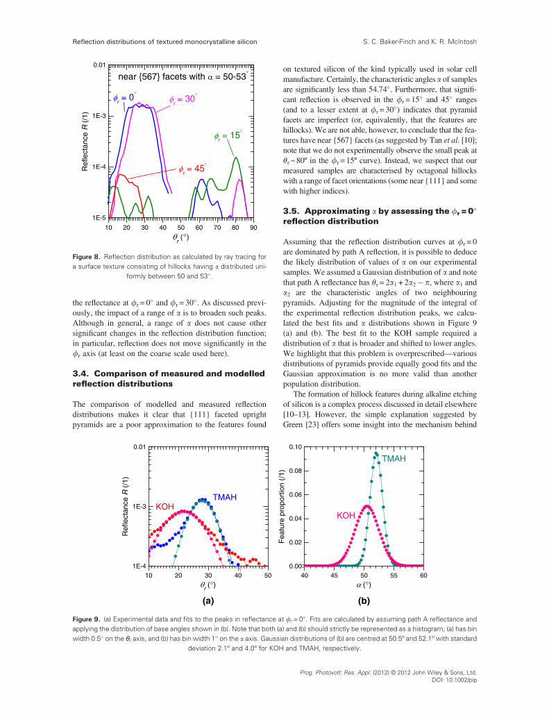
10 20 30 40 50 60 70 80 90
1E-5
1E-4
1E-3
0.01
Ref
lect
ance
R (
/1)
r( )
near {567} facets with = 50-53
Figure 8. Reflection distribution as calculated by ray tracing fora surface texture consisting of hillocks having a distributed uni-
formly between 50 and 53�.
Reflection distributions of textured monocrystalline silicon S. C. Baker-Finch and K. R. McIntosh
the reflectance at fr = 0� and fr = 30�. As discussed previ-ously, the impact of a range of a is to broaden such peaks.Although in general, a range of a does not cause othersignificant changes in the reflection distribution function;in particular, reflection does not move significantly in thefr axis (at least on the coarse scale used here).
3.4. Comparison of measured and modelledreflection distributions
The comparison of modelled and measured reflectiondistributions makes it clear that {111} faceted uprightpyramids are a poor approximation to the features found
10 20 30 40 501E-4
1E-3
0.01
(a)
Ref
lect
ance
R (
/1)
r( )
TMAHKOH
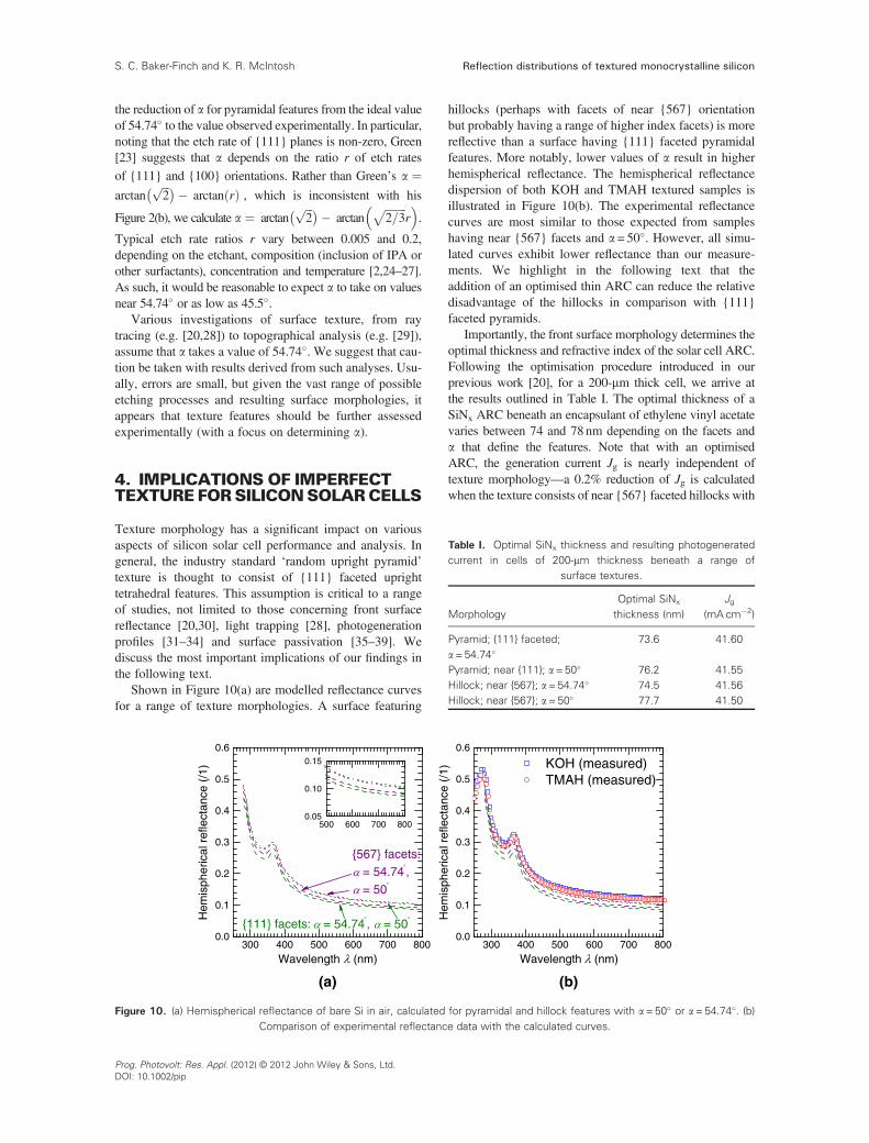
Figure 9. (a) Experimental data and fits to the peaks in reflectance aapplying the distribution of base angles shown in (b). Note that both (awidth 0.5� on the θr axis, and (b) has bin width 1� on the a axis. Gaussi
deviation 2.1º and 4.0º for KOH
on textured silicon of the kind typically used in solar cellmanufacture. Certainly, the characteristic angles a of samplesare significantly less than 54.74�. Furthermore, that signifi-cant reflection is observed in the fr = 15� and 45� ranges(and to a lesser extent at fr = 30�) indicates that pyramidfacets are imperfect (or, equivalently, that the features arehillocks). We are not able, however, to conclude that the fea-tures have near {567} facets (as suggested by Tan et al. [10];note that we do not experimentally observe the small peak atθr ~ 80º in the fr = 15º curve). Instead, we suspect that ourmeasured samples are characterised by octagonal hillockswith a range of facet orientations (some near {111} and somewith higher indices).
3.5. Approximating a by assessing the fr =0�
reflection distribution
Assuming that the reflection distribution curves at fr = 0are dominated by path A reflection, it is possible to deducethe likely distribution of values of a on our experimentalsamples. We assumed a Gaussian distribution of a and notethat path A reflectance has θr = 2a1 + 2a2� p, where a1 anda2 are the characteristic angles of two neighbouringpyramids. Adjusting for the magnitude of the integral ofthe experimental reflection distribution peaks, we calcu-lated the best fits and a distributions shown in Figure 9(a) and (b). The best fit to the KOH sample required adistribution of a that is broader and shifted to lower angles.We highlight that this problem is overprescribed—variousdistributions of pyramids provide equally good fits and theGaussian approximation is no more valid than anotherpopulation distribution.
The formation of hillock features during alkaline etchingof silicon is a complex process discussed in detail elsewhere[10–13]. However, the simple explanation suggested byGreen [23] offers some insight into the mechanism behind
0.00
0.02
0.04
0.06
0.08
0.10
40 45 50 55 60
TMAH
KOH
Fea
ture
pro
port
ion
(/1)
( )
(b)
t fr = 0�. Fits are calculated by assuming path A reflectance and) and (b) should strictly be represented as a histogram; (a) has binan distributions of (b) are centred at 50.5º and 52.1º with standardand TMAH, respectively.
Prog. Photovolt: Res. Appl. (2012) © 2012 John Wiley & Sons, Ltd.DOI: 10.1002/pip
Reflection distributions of textured monocrystalline siliconS. C. Baker-Finch and K. R. McIntosh
the reduction of a for pyramidal features from the ideal valueof 54.74� to the value observed experimentally. In particular,noting that the etch rate of {111} planes is non-zero, Green[23] suggests that a depends on the ratio r of etch rates
of {111} and {100} orientations. Rather than Green’s a ¼arctan
ffiffiffi2
p� �� arctan rð Þ , which is inconsistent with his
Figure 2(b), we calculate a ¼ arctanffiffiffi2
p� �� arctanffiffiffiffiffiffiffiffi2=3
pr
� �.
Typical etch rate ratios r vary between 0.005 and 0.2,depending on the etchant, composition (inclusion of IPA orother surfactants), concentration and temperature [2,24–27].As such, it would be reasonable to expect a to take on valuesnear 54.74� or as low as 45.5�.
Various investigations of surface texture, from raytracing (e.g. [20,28]) to topographical analysis (e.g. [29]),assume that a takes a value of 54.74�. We suggest that cau-tion be taken with results derived from such analyses. Usu-ally, errors are small, but given the vast range of possibleetching processes and resulting surface morphologies, itappears that texture features should be further assessedexperimentally (with a focus on determining a).
Table I. Optimal SiNx thickness and resulting photogeneratedcurrent in cells of 200-mm thickness beneath a range of
surface textures.
MorphologyOptimal SiNx
thickness (nm)Jg
(mA cm�2)
Pyramid; {111} faceted;a=54.74�
73.6 41.60
Pyramid; near {111}; a=50� 76.2 41.55Hillock; near {567}; a=54.74� 74.5 41.56Hillock; near {567}; a=50� 77.7 41.50
4. IMPLICATIONS OF IMPERFECTTEXTUREFORSILICONSOLARCELLS
Texture morphology has a significant impact on variousaspects of silicon solar cell performance and analysis. Ingeneral, the industry standard ‘random upright pyramid’texture is thought to consist of {111} faceted uprighttetrahedral features. This assumption is critical to a rangeof studies, not limited to those concerning front surfacereflectance [20,30], light trapping [28], photogenerationprofiles [31–34] and surface passivation [35–39]. Wediscuss the most important implications of our findings inthe following text.
Shown in Figure 10(a) are modelled reflectance curvesfor a range of texture morphologies. A surface featuring
0.0
0.1
0.2
0.3
0.4
0.5
0.6
300 400 500 600 700 800
5000.05
0.10
0.15
(a)
{567} facets: = 54.74 , = 50
Hem
isph
eric
al r
efle
ctan
ce (
/1)
Wavelength (nm)
{111} facets: = 54.74 , = 50
800700600
Figure 10. (a) Hemispherical reflectance of bare Si in air, calculatedComparison of experimental reflectanc
Prog. Photovolt: Res. Appl. (2012) © 2012 John Wiley & Sons, Ltd.DOI: 10.1002/pip
hillocks (perhaps with facets of near {567} orientationbut probably having a range of higher index facets) is morereflective than a surface having {111} faceted pyramidalfeatures. More notably, lower values of a result in higherhemispherical reflectance. The hemispherical reflectancedispersion of both KOH and TMAH textured samples isillustrated in Figure 10(b). The experimental reflectancecurves are most similar to those expected from sampleshaving near {567} facets and a= 50�. However, all simu-lated curves exhibit lower reflectance than our measure-ments. We highlight in the following text that theaddition of an optimised thin ARC can reduce the relativedisadvantage of the hillocks in comparison with {111}faceted pyramids.
Importantly, the front surface morphology determines theoptimal thickness and refractive index of the solar cell ARC.Following the optimisation procedure introduced in ourprevious work [20], for a 200-mm thick cell, we arrive atthe results outlined in Table I. The optimal thickness of aSiNx ARC beneath an encapsulant of ethylene vinyl acetatevaries between 74 and 78nm depending on the facets anda that define the features. Note that with an optimisedARC, the generation current Jg is nearly independent oftexture morphology—a 0.2% reduction of Jg is calculatedwhen the texture consists of near {567} faceted hillocks with
300 400 500 600 700 8000.0
0.1
0.2
0.3
0.4
0.5
0.6
(b)
KOH (measured) TMAH (measured)
Hem
isph
eric
al r
efle
ctan
ce (
/1)
Wavelength (nm)
for pyramidal and hillock features with a=50� or a=54.74�. (b)e data with the calculated curves.
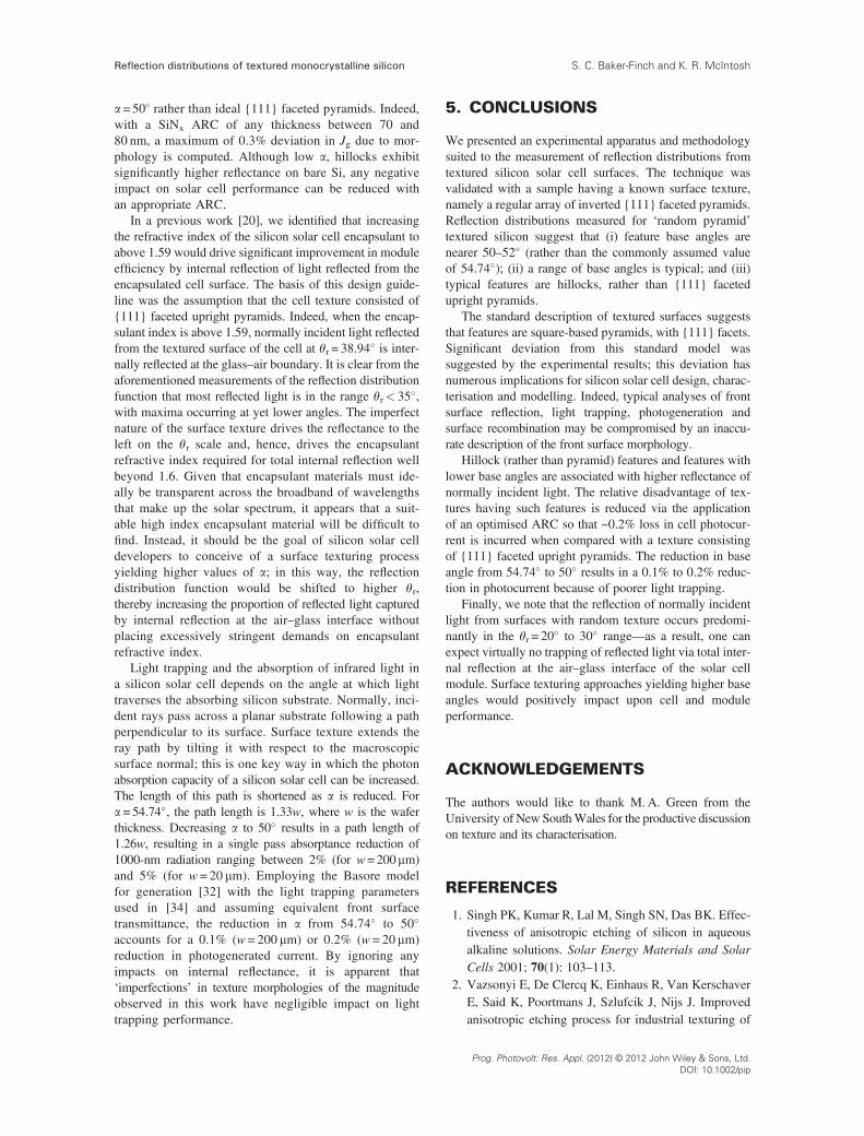
Reflection distributions of textured monocrystalline silicon S. C. Baker-Finch and K. R. McIntosh
a=50� rather than ideal {111} faceted pyramids. Indeed,with a SiNx ARC of any thickness between 70 and80 nm, a maximum of 0.3% deviation in Jg due to mor-phology is computed. Although low a, hillocks exhibitsignificantly higher reflectance on bare Si, any negativeimpact on solar cell performance can be reduced withan appropriate ARC.
In a previous work [20], we identified that increasingthe refractive index of the silicon solar cell encapsulant toabove 1.59 would drive significant improvement in moduleefficiency by internal reflection of light reflected from theencapsulated cell surface. The basis of this design guide-line was the assumption that the cell texture consisted of{111} faceted upright pyramids. Indeed, when the encap-sulant index is above 1.59, normally incident light reflectedfrom the textured surface of the cell at θr = 38.94� is inter-nally reflected at the glass–air boundary. It is clear from theaforementioned measurements of the reflection distributionfunction that most reflected light is in the range θr< 35�,with maxima occurring at yet lower angles. The imperfectnature of the surface texture drives the reflectance to theleft on the θr scale and, hence, drives the encapsulantrefractive index required for total internal reflection wellbeyond 1.6. Given that encapsulant materials must ide-ally be transparent across the broadband of wavelengthsthat make up the solar spectrum, it appears that a suit-able high index encapsulant material will be difficult tofind. Instead, it should be the goal of silicon solar celldevelopers to conceive of a surface texturing processyielding higher values of a; in this way, the reflectiondistribution function would be shifted to higher θr,thereby increasing the proportion of reflected light capturedby internal reflection at the air–glass interface withoutplacing excessively stringent demands on encapsulantrefractive index.
Light trapping and the absorption of infrared light ina silicon solar cell depends on the angle at which lighttraverses the absorbing silicon substrate. Normally, inci-dent rays pass across a planar substrate following a pathperpendicular to its surface. Surface texture extends theray path by tilting it with respect to the macroscopicsurface normal; this is one key way in which the photonabsorption capacity of a silicon solar cell can be increased.The length of this path is shortened as a is reduced. Fora=54.74�, the path length is 1.33w, where w is the waferthickness. Decreasing a to 50� results in a path length of1.26w, resulting in a single pass absorptance reduction of1000-nm radiation ranging between 2% (for w=200mm)and 5% (for w = 20 mm). Employing the Basore modelfor generation [32] with the light trapping parametersused in [34] and assuming equivalent front surfacetransmittance, the reduction in a from 54.74� to 50�
accounts for a 0.1% (w = 200 mm) or 0.2% (w = 20 mm)reduction in photogenerated current. By ignoring anyimpacts on internal reflectance, it is apparent that‘imperfections’ in texture morphologies of the magnitudeobserved in this work have negligible impact on lighttrapping performance.
5. CONCLUSIONS
We presented an experimental apparatus and methodologysuited to the measurement of reflection distributions fromtextured silicon solar cell surfaces. The technique wasvalidated with a sample having a known surface texture,namely a regular array of inverted {111} faceted pyramids.Reflection distributions measured for ‘random pyramid’textured silicon suggest that (i) feature base angles arenearer 50–52� (rather than the commonly assumed valueof 54.74�); (ii) a range of base angles is typical; and (iii)typical features are hillocks, rather than {111} facetedupright pyramids.
The standard description of textured surfaces suggeststhat features are square-based pyramids, with {111} facets.Significant deviation from this standard model wassuggested by the experimental results; this deviation hasnumerous implications for silicon solar cell design, charac-terisation and modelling. Indeed, typical analyses of frontsurface reflection, light trapping, photogeneration andsurface recombination may be compromised by an inaccu-rate description of the front surface morphology.
Hillock (rather than pyramid) features and features withlower base angles are associated with higher reflectance ofnormally incident light. The relative disadvantage of tex-tures having such features is reduced via the applicationof an optimised ARC so that ~0.2% loss in cell photocur-rent is incurred when compared with a texture consistingof {111} faceted upright pyramids. The reduction in baseangle from 54.74� to 50� results in a 0.1% to 0.2% reduc-tion in photocurrent because of poorer light trapping.
Finally, we note that the reflection of normally incidentlight from surfaces with random texture occurs predomi-nantly in the θr = 20� to 30� range—as a result, one canexpect virtually no trapping of reflected light via total inter-nal reflection at the air–glass interface of the solar cellmodule. Surface texturing approaches yielding higher baseangles would positively impact upon cell and moduleperformance.
ACKNOWLEDGEMENTS
The authors would like to thank M.A. Green from theUniversity of New SouthWales for the productive discussionon texture and its characterisation.
REFERENCES
1. Singh PK, Kumar R, Lal M, Singh SN, Das BK. Effec-tiveness of anisotropic etching of silicon in aqueousalkaline solutions. Solar Energy Materials and SolarCells 2001; 70(1): 103–113.
2. Vazsonyi E, De Clercq K, Einhaus R, Van KerschaverE, Said K, Poortmans J, Szlufcik J, Nijs J. Improvedanisotropic etching process for industrial texturing of
Prog. Photovolt: Res. Appl. (2012) © 2012 John Wiley & Sons, Ltd.DOI: 10.1002/pip
Reflection distributions of textured monocrystalline siliconS. C. Baker-Finch and K. R. McIntosh
silicon solar cells. Solar Energy Materials and SolarCells 1999; 57(2): 179–188.
3. Nishimoto Y, Namba K. Investigation of texturisationfor crystalline silicon solar cells with sodium carbonatesolutions. Solar Energy Materials and Solar Cells2000; 61(4): 393–402.
4. Melnyk I, Wefringhaus E, McCann M, Hefricht A,Hauser A, Fath P. Na2CO3 as an alternative to\NaOH/IPA for texturization of monocrystalline silicon.Proceedings of the 19th European Photovoltaic SolarEnergy Conference, Paris, 2004; 1090–1093.
5. Marrero N, Gonzalez-Diaz B, Guerrero-Lemus R,Borchert D, Hernandez-Rodriguez C. Optimization ofsodium carbonate texturization on large-area crystallinesilicon solar cells. Solar Energy Materials and SolarCells 2007; 91(20): 1943–1947.
6. King DL, Buck ME. Experimental optimization of ananisotropic etching process for random texturizationof silicon solar cells. Proceedings of the 22nd IEEEPhotovoltaic Specialists Conference, Las Vegas, 1991
7. You JS, Kim D, Huh JY, Park HJ, Pak JJ, Kang CS.Experiments on anisotropic etching of Si in TMAH.Proceedings of the 11th International PhotovoltaicScience and Engineering Conference, Hokkaido,1999; 981–984.
8. Papet P, Nichiporuk O, Kaminski A, Rozier Y, KraiemJ, Lelievre, JF, Chaumartin A, Fave A, Lemiti M.Pyramidal texturing of silicon solar cell with TMAHchemical anisotropic etching. Solar Energy Materialsand Solar Cells 2006; 90(15): 2319–2328.
9. Ximello N, Dastgheib-Shirazi A, Scholz S, Hahn G.Influence of pyramid size of chemically textured sili-con wafers on the characteristics of industrial solarcells. Proceedings of the 25th European PhotovoltaicSolar Energy Conference, Valencia, 2010; 1761–1764.
10. Tan S-S, Reed M, Han H, Boudreau R. Morphology ofetch hillock defects created during anisotropic etchingof silicon. Journal of Micromechanics and Microengi-neering 1994; 4: 147–155.
11. Bhatnagar YK, Nathan A. On pyramidal protrusions inanisotropic etching of <100> silicon. Sensors andActuators A 1993; 36: 233–240.
12. Landsberger LM, Naseh S, Kahrizi M, Paranjape M.On hillocks generated during anisotropic etching ofSi in TMAH. Journal of MicroelectromechanicalSystems 1996; 5(2): 106–116.
13. Thong JTL, Luo P, Choi WK, Tan SC. Evolution ofhillocks during silicon etching in TMAH. Journal ofMicromechanics and Microengineering 2001; 11:61–69.
14. Zubel I, Kramkowska M. Development of etch hil-locks on different Si(hkl) planes in silicon anisotropicetching. Surface Science 2008; 602: 1712–1721.
Prog. Photovolt: Res. Appl. (2012) © 2012 John Wiley & Sons, Ltd.DOI: 10.1002/pip
15. Fornies E, Zaldo C, Albella JM. Control of randomtexture of monocrystalline silicon cells by angle-resolved optical reflectance. Solar Energy Materialsand Solar Cells 2005; 87(1–4): 583–593.
16. Mackel H, Cambre DM, Zaldo C, Albella JM, SanchezS, Vazquez C, Sanchez I, Vazquez MA. Characterisa-tion of monocrystalline silicon texture using opticalreflectance patterns. Proceedings of the 23rd EuropeanPhotovoltaic Solar Energy Conference, Valencia,2008; 1160–1163.
17. Parretta A. Camera for recording light backscatteredfrom textured photovoltaic samples. Journal of OpticsA: Pure and Applied Optics 2003; 5: S284–S292.
18. Parretta A, Bobeico E, Lancellotti L, Morvillo P,Wang A, Zhao J. A new approach to the analysis oflight collected by textured silicon surfaces. Proceedingsof the 3rd World Conference on Photovoltaic EnergyConversion, Osaka, 2003; 122–125.
19. FoldynaM,MorenoM, Roca i Cabarrocas P, DeMartinoA.Scattered light measurements on textured crystallinesilicon substrates using an angle-resolved Muellermatrix polarimeter. Applied Optics 2010; 49(3): 505–512.
20. Baker-Finch SC, McIntosh KR. Reflection of normallyincident light from silicon solar cells with pyramidaltexture. Progress in Photovoltaics: Research andApplications 2011; 19: 406–416.
21. Van Nijnatten PA. Optical analysis of coatings byvariable angle spectrophotometry. Thin Solid Films2008; 516: 4553–4557.
22. Van Nijnatten PA. An automated directional reflec-tance/transmittance analyser for coating analysis. ThinSolid Films 2003; 442: 74–79.
23. Green MA. Analytical expressions for spectral compo-sition of band photoluminescence from silicon wafersand bricks. Applied Physics Letters 2011; 99: 131112.
24. Price JB. Anisotropic etching of silicon with KOH-H2O-Isopropyl Alcohol. Semiconductor Silicon 1973,eds. HR Huff and RR Burgess (The ElectrochemicalSociety, Princeton NJ) 1973; 339–353.
25. Merlos A, Acero M, Bao MH, Bausells J, Esteve J.TMAH/IPA anisotropic etching characteristics. Sensorsand Actuators A 1993; 37–38: 737–743.
26. Sekimua M. Anisotropic etching of surfactant-addedTMAH solution. Proceedings of the 12th IEEE Inter-national Conference on Micro Electro MechanicalSystems, Orlando, 1999: 650–655.
27. Wind RA, Hines MA. Macroscopic etch anisotropiesand microscopic reaction mechanisms: a microma-chined structure for the rapid assay of etchant anisot-ropy. Surface Science 2000; 460: 21–38
28. Campbell PA, Green MA. Light trapping properties ofpyramidally textured surfaces. Journal of AppliedPhysics 1987; 62(1): 243–249.
Reflection distributions of textured monocrystalline silicon S. C. Baker-Finch and K. R. McIntosh
29. Wefringhaus E, Kesnar C, Lohmann M. Statisticalapproach to the description of random pyramidsurfaces using 3D surface profiles. Energy Procedia2011; 8: 135–140.
30. Chiao S-C, Zhou J-L, Macleod HA. Optimized designof an antireflection coating for textured silicon solarcells. Applied Optics 1993; 32(28): 5557–5560.
31. Basore PA. Numerical modelling of textured siliconsolar cells using PC-1D. IEEE Transactions on ElectronDevices 1990; 37(2): 337–343.
32. Basore PA. Extended spectral analysis of internalquantum efficiency. Proceedings of the 23rd IEEEPhotovoltaics Specialists Conference, 1993; 147–152.
33. Brendel R, Hirsch M, Plieninger R, Werner JH.Wuantum efficiency analysis of thin-layer silicon solarcells with back surface fields and optical confinement.IEEE Transactions on Electron Devices 1996; 43(7):1104–1113.
34. Baker-Finch SC, McIntosh KR. One-dimensionalphotogeneration profiles in silicon solar cells withpyramidal texture. Progress in Photovoltaics: Researchand Applications 2011. DOI: 10.1002/pip.1109.
35. Cousins PJ, Cotter JE. Minimizing lifetime degrada-tion associated with thermal oxidation of uprightrandomly textured silicon surfaces. Solar EnergyMaterials and Solar Cells 2006; 2(90): 228–240.
36. Chen FW, Li T-TA, Cotter JE. PECVD siliconnitride surface passivation for high-efficiency n-typesilicon solar cells. Proceedings of the 4th WorldConference on Photovoltaic Energy Conversion,2006; 1020–1023.
37. McIntosh KR, Johnson LP. Recombination at texturedsilicon surfaces passivated with silicon dioxide.Journal of Applied Physics 2009; 105: 124520.
38. Gong C, Simoen E, Posthuma NE, Van Kerschaver E,Poortmans J, Mertens R. Study of silicon-siliconnitride interface properties on planar (100), planar(111) and textured surfaces using deep-level transientspectroscopy. Journal of Physics D: Applied Phyics2010; 43: 485301-1-6.
39. Baker-Finch SC, McIntosh KR. The contribution ofplanes, vertices and edges to recombination at pyrami-dally textured surfaces. IEEE Journal of Photovoltaics2011. DOI: 10.1109/jphotov.2011.2165530.
Prog. Photovolt: Res. Appl. (2012) © 2012 John Wiley & Sons, Ltd.DOI: 10.1002/pip