Embed Size (px)
Citation preview

www.afm-journal.de
FULL P
APER
© 2014 WILEY-VCH Verlag GmbH & Co. KGaA, Weinheim 1
www.MaterialsViews.com
wileyonlinelibrary.com
wearable computing and medical robotics that depend on mechanical impedence matching with natural human tissue. However, progress in these applica-tion domains requires more versatile methods to simultaneously pattern thin fi lms of conductive elastomer and liquid GaIn for rapid integration into circuits and sensor arrays. For example, poly(dimethylsiloxane) (PDMS) fi lled with carbon nanotubes or other conductive microparticles (cPDMS) such as nickel or silver may be patterned through replica molding [ 25,26 ] or microcontact printing. [ 27 ] In the case of liquid GaIn alloys, pat-terning is currently performed with needle injection, inkjet printing, [ 28 ] masked deposition, [ 29 ] and microcontact printing (μCP). [ 30 ] While reliable, these existing methods typically require photolithog-raphy or customized printing hardware
and can be costly and time consuming. An exception is the method presented in [ 26 ] in which a commercial excimer laser (wavelength, λ = 248 nm) is used to produce molds for casting cPDMS. Another approach is stencil lithography, which has been recently applied to liquid GaIn. [ 22,31,32 ] However, although it is rapid and inexpensive, stencil lithography can only be used to produce a limited range of circuit geometries.
In this manuscript, we introduce a method for pro-ducing soft-matter electronic circuits by patterning thin fi lms of cPDMS and liquid-phase EGaIn alloy with a CO 2 laser (10.6 μm wavelength). This rapid prototyping approach to fab-rication eliminates the need for photolithography or custom-ized printing hardware. Moreover, we demonstrate the ability to laser-pattern EGaIn through a mechanism that exploits the unique “moldability” of the liquid alloy. Figure 1 presents exam-ples of how CO 2 laser patterning is used to produce soft-matter sensors for electronic skin applications. These include a fi n-gertip mounted carbon-based cPDMS sensor for detecting skin contact (Figure 1 a), a miniaturized multi-layered carbon-based cPDMS sensor array (Figure 1 b), and inclusions of PEDOT:PSS embedded in PDMS (Figure 1 c) and urethane (Figure 1 d). The test patterns in Figure 1 e are produced by using the CO 2 laser to pattern a thin layer of EGaIn alloy sandwiched between two layers of PDMS. After the excess EGaIn and elastomer are removed, the patterned fi lm is sealed in additional PDMS. Figures 1 f,g present an integrated circuits composed of serpen-tine EGaIn wires and cPDMS pads for mounting an LED and connecting to an external power supply.
CO 2 laser ablation has been previously used to produce microfl uidic channels in PMMA [ 33 ] and PDMS. [ 34 ] Polymers are typically patterned through a combination of vaporization and
Rapid Prototyping for Soft-Matter Electronics
Tong Lu , Lauren Finkenauer , James Wissman , and Carmel Majidi *
A series of rapid and inexpensive methods to produce elastically soft sensors and circuits in minutes using a CO 2 laser (10.6 μm wavelength) are intro-duced. These soft-matter electronics are composed of laser-patterned fi lms of conductive poly(dimethylsiloxane) (cPDMS) and liquid-phase gallium–indium (GaIn) alloy embedded in a thin sheet of soft silicone elastomer. Direct laser patterning eliminates the need for photolithography, replica molding, and customized inkjet or microcontact (μCP) printing, and allows conductive traces of cPDMS and liquid GaIn to be rapidly integrated into a single soft-matter circuit. The versatility of this fabrication method is demonstrated by the production of a variety of electrically functional soft-matter sensors and circuit elements that contain features with >150 μm planar dimensions. It is postulated that, in the case of GaIn alloy, patterning occurs when the recoil force of the escaping vapor exceeds the liquid’s surface tension. This mecha-nism exploits the unique “moldability” of liquid GaIn alloy, which forms a surface oxide of Ga 2 O 3 that allows the patterned fi lm to maintain its shape.
DOI: 10.1002/adfm.201303732
T. Lu, L. Finkenauer, J. Wissman, Prof. C. Majidi Soft Machines Lab Department of Mechanical Engineering Carnegie Mellon University Pittsburgh , PA 15213 , USA E-mail: [email protected]
1. Introduction
Soft-matter electronics are composed of electrically conductive fl uids, pastes, gels, and elastomers embedded in a thin fi lm of elastically soft material. [ 1–6 ] In contrast to conventional elec-tronics, these devices contain no rigid materials and remain electrically functional when stretched to several times their natural length. In this respect, soft-matter electronics comple-ment other stretchable circuit technologies based on carbon nanotubes, [ 7,8 ] graphene, [ 9 ] and wavy circuit wiring. [ 10,11 ] In recent years, stretchable electronics have been produced by embedding a thin fi lm of soft silicone elastomer with micro-fl uidic channels of liquid-phase gallium–indium alloy. Liquid GaIn has 1/20 th the conductivity of copper wiring and remains intact as the surrounding elastomer is stretched. Liquid GaIn alloys such as EGaIn (eutectic gallium–indium) and Galinstan (gallium–indium–tin) have been used as highly stretchable electrical wiring, [ 12,13 ] elastically tunable antennae for wireless communication, [ 14–16 ] logic gates and diodes for elastically soft digital circuits, [ 17,18 ] and hyperelastic sensors for measuring pressure, [ 19,20 ] strain, [ 21 ] friction, [ 22,23 ] and bending curvature. [ 24 ]
Because of their intrinsic elasticity, soft-matter electronics have a potentially central role in applications like
Adv. Funct. Mater. 2014, DOI: 10.1002/adfm.201303732

FULL
PAPER
2
www.afm-journal.dewww.MaterialsViews.com
wileyonlinelibrary.com © 2014 WILEY-VCH Verlag GmbH & Co. KGaA, Weinheim
the displacement of molten polymer. Molten polymer is dis-placed when the pressure of the escaping vapor (recoil force) exceeds the surface tension of the liquid. We postulate that thin fi lms of PDMS fi lled with conductive microparticles can be similarly patterned with a CO 2 laser. This includes carbon-based cPDMS, such as PDMS fi lled with acetylene carbon black, and PDMS fi lled with silver and nickel microparticles.
In contrast to elastomers, liquid-phase GaIn metal alloys cannot be ablated with a CO 2 laser. As with other metals, EGaIn would require a high-energy UV radiation source for photo-chemical ablation. Instead, we postulate that EGaIn is removed with the same liquid metal expulsion mechanisms used in CO 2 laser beam welding (LBW). [ 35 ] However, whereas stainless steel, titanium, and other solid metals require a high power to ini-tiate melting (>1 kW for CO 2 lasers), GaIn alloys are already molten at room temperature and, as with molten polymer, can be displaced by pressure from the vapor escaping the PDMS beneath. In addition to being in a liquid state, GaIn alloys form a surface oxide of Ga 2 O 3 that prevents the liquid from fl owing back into the laser-patterned region. In other words, this prop-erty of “moldability” enabled by the oxide skin [ 36–39 ] allows the liquid to retain its shape after it has been patterned. Since they have both low fl uidic viscosity and a high surface tension, GaIn alloys can simultaneously behave like a solid and a liquid at sub-millimeter length scales. This unique combination of prop-erties enables the rare ability to pattern a metal alloy with an inexpensive laser engraving system that operates at relatively high wavelengths (10.6 μm) and low power (1–30 W).
2. Results
We use a 30 W CO 2 laser (VLS 3.50; Universal Laser Systems, Inc.) to pattern thin fi lms of electrically conductive cPDMS and EGaIn and produce elastic, soft sensors and circuit elements.
The methods for patterning cPDMS and a multi-layered circuit are presented in Figure 2 a. As discussed in the Experimental Section below, carbon-based cPDMS is composed of 84 wt% 20:1 PDMS (Sylgard 184; Dow Corning, Inc.) mixed with 16 wt% acetylene carbon black powder (Alfa Aesar). We have also patterned fi lms of cPDMS containing either 84% silver microparticles (2–3.5 μm; Sigma Aldrich, Inc.) or a combina-tion of 65% nickel and 25% silver (NuSil R-2637; NuSil Tech-nology LLC). First, a thin fi lm of cPDMS is applied by spin coating the uncured elastomer on a brass sheet and laser-pat-terning it after curing (i), followed by removal of the excess cPDMS (ii). The brass sheet is fi nally coated with a sealing layer of non-conductive PDMS before peeling the cured fi lm from the brass cutting surface (iii). For this sequence of steps, which was used to produce the tactile sensor in Figure 1 a, the embedded cPDMS circuit is exposed and fl ush with the sur-rounding PDMS. However, to produce multi-layered circuits, such as the sensor array in Figure 1 b, additional layers of con-ductive and non-conductive PDMS must be added. For a multi-layered circuit, the “bottom” layer is patterned and sealed as before (i–iii). After removal of this sheet, the cutting surface is coated with a new layer of cPDMS and subsequently PDMS after curing (iv). The two layers are then patterned with the laser (v) before a fi nal coating of PDMS (vi) and removal of excess material (vii). The uncured PDMS deposited after pat-terning the two sheets (vi) acts as an adhesive fi lm for bonding the “top” layer with the previously fabricated bottom layer (viii). Lastly, the completely cured multi-layered circuit is peeled from the cutting surface (ix).
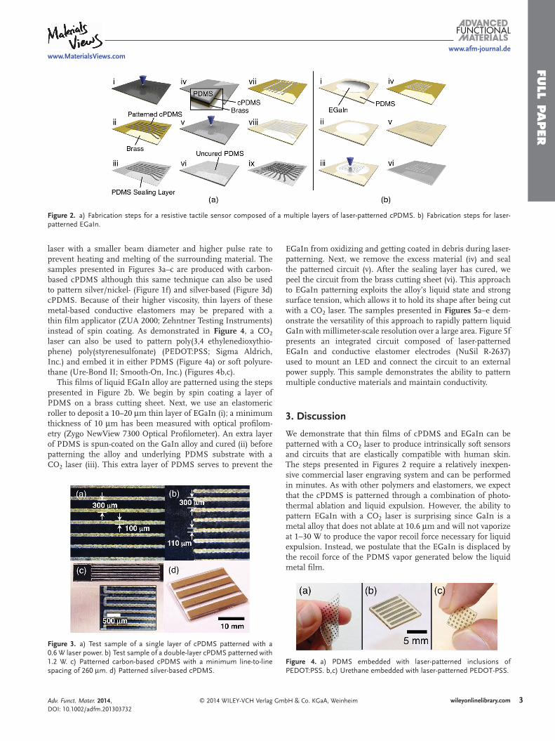
Figures 3 b,c demonstrate CO 2 laser machining of single and double-layers of cPDMS with laser powers of 0.6 and 1.2 W, respectively. For a single layer of cPDMS, a minimum line-to-line spacing of 260 μm is possible (Figure 3 c). This maximum resolution is limited by the laser spot size and pulse rate. Smaller feature sizes can be achieved by a lower wavelength
Adv. Funct. Mater. 2014, DOI: 10.1002/adfm.201303732
Figure 1. a) Resistive tactile sensor composed of laser-patterned conductive poly(dimethylsiloxane) (cPDMS). b) Sensor array composed of overlap-ping strips of cPDMS insulated by non-conductive elastomer. c) Laser-patterned inclusions of PEDOT:PSS embedded in PDMS. d) Laser-patterned PEDOT:PSS embedded in polyurethane. e) Laser-patterned eutectic Gallium-Indium alloy (EGaIn) embedded in PDMS. f) Integration of a serpentine EGaIn wire and cPDMS electrodes in a PDMS-sealed circuit. g) LED-embedded circuit composed of laser-patterned cPDMS and EGaIn.
FULL P
APER
3
www.afm-journal.dewww.MaterialsViews.com
wileyonlinelibrary.com© 2014 WILEY-VCH Verlag GmbH & Co. KGaA, Weinheim
laser with a smaller beam diameter and higher pulse rate to prevent heating and melting of the surrounding material. The samples presented in Figures 3 a–c are produced with carbon-based cPDMS although this same technique can also be used to pattern silver/nickel- (Figure 1 f) and silver-based (Figure 3 d) cPDMS. Because of their higher viscosity, thin layers of these metal-based conductive elastomers may be prepared with a thin fi lm applicator (ZUA 2000; Zehntner Testing Instruments) instead of spin coating. As demonstrated in Figure 4 , a CO 2 laser can also be used to pattern poly(3,4 ethylenedioxythio-phene) poly(styrenesulfonate) (PEDOT:PSS; Sigma Aldrich, Inc.) and embed it in either PDMS (Figure 4 a) or soft polyure-thane (Ure-Bond II; Smooth-On, Inc.) (Figures 4 b,c).
This fi lms of liquid EGaIn alloy are patterned using the steps presented in Figure 2 b. We begin by spin coating a layer of PDMS on a brass cutting sheet. Next, we use an elastomeric roller to deposit a 10–20 μm thin layer of EGaIn (i); a minimum thickness of 10 μm has been measured with optical profi lom-etry (Zygo NewView 7300 Optical Profi lometer). An extra layer of PDMS is spun-coated on the GaIn alloy and cured (ii) before patterning the alloy and underlying PDMS substrate with a CO 2 laser (iii). This extra layer of PDMS serves to prevent the
EGaIn from oxidizing and getting coated in debris during laser-patterning. Next, we remove the excess material (iv) and seal the patterned circuit (v). After the sealing layer has cured, we peel the circuit from the brass cutting sheet (vi). This approach to EGaIn patterning exploits the alloy’s liquid state and strong surface tension, which allows it to hold its shape after being cut with a CO 2 laser. The samples presented in Figures 5 a–e dem-onstrate the versatility of this approach to rapidly pattern liquid GaIn with millimeter-scale resolution over a large area. Figure 5 f presents an integrated circuit composed of laser-patterned EGaIn and conductive elastomer electrodes (NuSil R-2637) used to mount an LED and connect the circuit to an external power supply. This sample demonstrates the ability to pattern multiple conductive materials and maintain conductivity.
3. Discussion
We demonstrate that thin fi lms of cPDMS and EGaIn can be patterned with a CO 2 laser to produce intrinsically soft sensors and circuits that are elastically compatible with human skin. The steps presented in Figures 2 require a relatively inexpen-sive commercial laser engraving system and can be performed in minutes. As with other polymers and elastomers, we expect that the cPDMS is patterned through a combination of photo-thermal ablation and liquid expulsion. However, the ability to pattern EGaIn with a CO 2 laser is surprising since GaIn is a metal alloy that does not ablate at 10.6 μm and will not vaporize at 1–30 W to produce the vapor recoil force necessary for liquid expulsion. Instead, we postulate that the EGaIn is displaced by the recoil force of the PDMS vapor generated below the liquid metal fi lm.
Adv. Funct. Mater. 2014, DOI: 10.1002/adfm.201303732
Figure 2. a) Fabrication steps for a resistive tactile sensor composed of a multiple layers of laser-patterned cPDMS. b) Fabrication steps for laser-patterned EGaIn.
Figure 3. a) Test sample of a single layer of cPDMS patterned with a 0.6 W laser power. b) Test sample of a double-layer cPDMS patterned with 1.2 W. c) Patterned carbon-based cPDMS with a minimum line-to-line spacing of 260 μm. d) Patterned silver-based cPDMS.
Figure 4. a) PDMS embedded with laser-patterned inclusions of PEDOT:PSS. b,c) Urethane embedded with laser-patterned PEDOT-PSS.

FULL
PAPER
4
www.afm-journal.dewww.MaterialsViews.com
wileyonlinelibrary.com © 2014 WILEY-VCH Verlag GmbH & Co. KGaA, Weinheim
As illustrated in Figure 6 a, the liquid alloy is deposited between two thin layers of PDMS. When exposed to the laser, the sample is locally heated (Figure 6 b) and PDMS in the top and bottom layers is ablated (Figure 6 c). We then postulate that the vaporized polymer exerts suffi cient pressure on the EGaIn fi lm to penetrate through and escape (Figure 6 d). As in conventional laser beam welding (LBW), displacement occurs when the recoil force from this pressure exceeds the surface force supported by the surface tension γ 0 and yield stress τ 0 of the liquid. [ 35 ] These values are estimated by pendant droplet measurements on EGaIn, which suggest γ 0 ≈ 0.445 J m –2 and τ 0 ≈ 119 Pa. [ 40 ] Interestingly, pendant droplet experiments on Galinstan in pure nitrogen (<0.5 ppm O 2 ) show greater sur-face tension (0.535 J m -2 ) than in an oxygenated (500 ppm O 2 ) environment (0.510 J m -2 ). [ 39 ] In practice, the laser has a cut-ting radius of approximately r c = 50 μm, which implies that the vaporized polymer exerts pressure on a circular region of GaIn with a circumference η = 2π r c = 314 μm. For a fi lm thickness h = 10 μm and assuming γ 0 ≈ 0.5 J m –2 the force required to puncture the oxide skin and displace the liquid alloy is approx-imately F = η ( γ 0 + τ 0 h ) ≈ 157 μN. This corresponds to a dif-ference of 20 kPa between the local vapor pressure and the atmospheric pressure. For comparison, the recoil pressure of vapor under ambient conditions is estimated to be p r ≈ 0.55 p s ( T s ), where p s is the saturation vapor pressure and T s is the surface temperature of the melting substrate. [ 41 ] An approxi-
Adv. Funct. Mater. 2014, DOI: 10.1002/adfm.201303732
Figure 5. a,b) PDMS embedded with laser-patterned inclusions of EGaIn. c,d) Large area sample. e) Miniaturized features: 2 mm × 2 mm squares spaced 0.25, 0.5, and 1 mm apart; concentric rings with diameters of 1.5, 3, and 5 mm and widths of 0.25, 0.35, and 0.5 mm, respectively; circles with diameters of 0.5, 1, 1.5, and 2 mm; rectangular strips with widths of 0.3, 0.7, and 1 mm. f) LED circuit containing laser-patterned (Ag/Ni)cPDMS and EGaIn.
Figure 6. Proposed mechanism for expulsion of a thin fi lm of liquid GaIn alloy on a PDMS substrate. a) The liquid alloy is coated with a thin layer of PDMS to prevent oxidation and limit exposure to debris. b) When exposed to the laser, the sample is locally heated and c) PDMS from the top and bottom layers vaporize. d) When the pressure difference between the vaporized polymer and atmosphere exceed the surface tension of the liquid fi lm (including its Ga 2 O 3 skin), the vapor will puncture the liquid fi lm and escape.

FULL P
APER
5
www.afm-journal.dewww.MaterialsViews.com
wileyonlinelibrary.com© 2014 WILEY-VCH Verlag GmbH & Co. KGaA, Weinheim
mate estimate for p s is obtained from the Clausius-Clapeyron relation and Trouton’s rule (valid for many organic liquids): ln( p s / p atm ) ≈ −10.6( T v / T s – 1), where p atm = 101.3 kPa is the atmospheric pressure and T v is the boiling point of the molten polymer. [ 42 ] Assuming T v = 473 K and a surface temperature T s = 523 °C, that is, T s the recoil pressure will be approximately 152 kPa, which corresponds to a pressure difference of 50.7 kPa exerted on the liquid alloy fi lm. Another value for comparison is the direct radiation pressure exerted by the laser beam itself. For a maximum power of P = 30 W, this is approximately p = nP /π cr c 2 = 24.1 Pa, where n = 1.89 is the refractive index of the Ga 2 O 3 oxide surface [ 43 ] and c = 3 × 10 8 m s –1 is the speed of light. This is orders of magnitude less than the estimated pres-sure necessary to displace liquid GaIn and suggests that force from the beam alone is not suffi cient for patterning.
Referring to Figure 3 , linewidths of 118 μm are accom-plished with a cutting power of 0.6 W, PPI (pulses per inch) 1000, and speed 20%. Although not at the length scale neces-sary for microelectronics, 0.1–1 mm linewidths are adequate for a variety of sensing applications, including the contact detec-tion sensors presented in Figure 1 a,b. The sensor in Figure 1 a consists of a central electrode and four surrounding electrodes. When the fi ngertip makes simultaneous contact between the inner circle and one of the outer triangles, an electrical connec-tion is formed. Contact between different peripheral electrodes can be used to signal an "up", "down", "left", or "right" com-mand. Similarly, for the sensor in Figure 1 b, the location of the contacting fi ngertip can be determined by measuring the elec-trical resistance between electrode rows and columns at each node.
In this study, we have focused on elastically soft circuits with 0.1–1 mm linewidth circuit features that can be produced with a CO 2 laser. For microelectronics with 20–100 μm linewidths, a lower wavelength laser is required. The fundamental advan-tage of UV laser micromachining is the greater focal depth ( b ), and hence cutting depth, that can be achieved for a prescribed beam diameter (i.e., “waist size,” W 0 ). The VLS 3.50 CO 2 laser engraver used for fabricating these devices has a beam dia-meter of 100 μm. [ 44 ] For a Gaussian beam, b = 2π W 0 2 / λ , where W 0 is the minimum diameter of the beam (“waist size”) and λ is the wavelength of the laser. [ 45 ] This implies that, in theory, a 355 nm Nd:YAG laser should have on the order of 30× the cutting depth of a 10.6 μm CO 2 laser. Also, the lower wave-length of a UV laser allows for a much higher pulse rate (e.g., ≈100 kHz). This prevents heat from accumulating outside of the beam path, which would lead to melting and burning in the surrounding material and hence result in wider cuts.
4. Conclusions
Using a commercial 30 W CO 2 laser, we are able to rapidly pro-duce elastically soft electronic circuits composed of patterned cPDMS, PEDOT:PSS, and liquid-phase EGaIn alloy embedded in a thin fi lm of PDMS. These circuits contain features with 0.1–1 mm linewidths and function as elastically stretchable wiring and sensors for measuring stretch, surface pressure, and friction. In the case of EGaIn, we postulate that patterning is accomplished with a mechanism that is analogous to the
liquid expulsion that occurs in high power (> 1 kW) laser beam welding (LBW). However, in contrast to LBW, recoil force does not come from the vaporized metal but is instead produced by vaporization of the underlying elastomer substrate. Moreover, because the liquid GaIn rapidly oxidizes in air, it forms a thin “oxide skin” that allows the patterned fi lm to hold its shape after laser cutting and during sealing.
Future efforts will focus on further miniaturization with a commercial UV laser. We expect that the smaller beam size (≈15 μm) and higher pulse rate (≈100 kHz) will allow for linewidths as small as 20 μm. We also expect that at UV wave-lengths (e.g., λ = 355 nm), the EGaIn can be patterned with photochemical ablation. This will eliminate the need to rely on the liquid expulsion mechanism presented in Figure 6 and instead allows the liquid alloy to be patterned on any substrate, including metal. UV laser machining will also allow us to pat-tern thin fi lms of metal-based cPDMS without burning. As with EGaIn, we expect that silver microparticles will vaporize through photochemical ablation when excited with λ = 355 nm radiation. Ultimately, we hope to have a universal protocol for using commercial laser micromachining to rapidly produce soft-matter electronics and hence eliminate the need for cus-tomized hardware or cleanroom fabrication.
5. Experimental Section Fabrication of Laser-Patterned Carbon-Filled cPDMS Circuits : The
carbon-fi lled cPDMS is made by mixing PDMS (Sylgard 184, Dow Corning, Inc.), acetylene carbon black powder (SigmaAldrich, Inc.) and hexane (SigmaAldrich, Inc) using a magnetic stir bar (Fisher Scientifi c, Inc.) to help disperse the mixture. The mixing ratio of PDMS is 20:1. The contents of carbon black, PDMS, and hexane are 8% wt, 42% wt, and 50% wt, respectively. First, conductive PDMS is spun coated on a piece of brass cutting surface. The spin coating includes two stages: in stage one and two, the spinning speeds are 700 and 2000 rpm, with corresponding durations of 9 and 25 s. After spin coating, the brass sheet is placed on a hot plate at 130 °C for 10 min to cure. Next, a laser engraver (VLS3.50; Universal Laser System, Inc.) is used to pattern the cPDMS. The settings are power of 0.6 W, 5% speed, and 1000 PPI. The patterning is repeated three times to make sure the cuts are all the way through and clean. The excess cPDMS is then manually removed with tweezers. After laser-patterning, PDMS (Sylgard 184; Dow Corning, Inc) with a base to crosslinking ratio of 10:1 is used to seal the circuit. The thickness of sealing layer can be determined by adjusting the settings of spin coating. Finally, the sealed circuit is peeled from the brass surface after curing at the same settings.
Fabrication of Laser-Patterned Silver-Filled cPDMS Circuits : Silver-fi lled cPDMS is made by mixing silver powder (Sigma-Aldrich, Inc.), PDMS (10:1 mixing ratio), and hexane (Sigma-Aldrich, Inc.) in a ratio of 42:8:50 with a sonicator (Branson, Inc.) for 10 min. A thin fi lm applicator (ZUA 2000; Zehntner Testing Instruments) is used to apply the layer. The thickness is set to be 500 μm. After curing at 130 °C for 10 min, the fi lm is laser-patterned with 3 W, 10% speed, and 1000 PPI. The remainder of the fabrication is identical to that of carbon fi lled cPDMS.
Fabrication of Laser-Patterned PEDOT:PSS : First a layer of PDMS is spun coat onto brass cutting surface at 1700 rpm for 5 s then cured. Next, PEDOT:PSS (662501, Sigma-Aldrich, Inc) is spun coat onto the PDMS at 400 rpm for 5 s and cured at 90 °C for 20 min and laser-patterned with power of 0.6 W, 5% speed, and 1000 PPI. The laser patterning is repeated twice. After removing the excess PDMS and PEDOT:PSS, the patterns are sealed with PDMS and the circuit is obtained. For PEDOT:PSS in urethane, we begin by spraying a mold release agent (Ease Release 200, Mann Release Technologies, Inc.)
Adv. Funct. Mater. 2014, DOI: 10.1002/adfm.201303732

FULL
PAPER
6
www.afm-journal.dewww.MaterialsViews.com
wileyonlinelibrary.com © 2014 WILEY-VCH Verlag GmbH & Co. KGaA, Weinheim
Received: November 3, 2013 Revised: December 3, 2013
Published online:
Adv. Funct. Mater. 2014, DOI: 10.1002/adfm.201303732
onto the brass cutting surface. Next, PEDOT:PSS is spun coat onto the brass cutting surface at 400 rpm for 5 s and cured at 90 °C for 20 min. Urethane (Ure-Bond, SmoothOn, Inc.) then is spun coat onto PEDOT:PSS at 1700 for 10 s and heated at 60 °C for 10 min. After curing, the urethane and PEDOT:PSS are laser-patterned twice with power of 0.9 W, speed 5%, and PPI 1000. Lastly, the patterns are sealed with Urethane and cured.
Fabrication of Laser-Patterned EGain Circuits : First a thin fi lm of PDMS is applied to a brass cutting surface by spin coating at 1000 rpm for 10 s. After curing at 130 °C for 10 min, we deposit a thin fi lm of EGaIn alloy on the PDMS fi lm using an elastomeric roller. Another layer of PDMS is spun-coated onto the EGaIn at 700 rpm for 9 s and 1700 rpm for 5 s. The PDMS with EGaIn is laser-patterned with power of 0.6 W, speed 5%, and PPI 1000. This process is then repeated three times. Lastly, the excess material is removed and the circuit is completed with a sealing layer of PDMS. For the combined LED-EGaIn-cPDMS circuit, we fi rst pattern NuSil R-2637 conductive elastomer to make the electrode pads for mounting the LED and connecting an external power supply. The cPDMS pads are sealed with non-conductive PDMS. After curing, the sample is turned over and coated with EGaIn. Another layer of PDMS is spun-coated on top of the EGaIn and cured. EGaIn is placed to partially overlap the electrode pads in order to establish an electrical connection. After the EGaIn is patterned, the excess material and the LED is mounted to the electrode pads. Lastly, the circuit is sealed in an addition layer of PDMS.
Acknowledgements This work was supported by a Defense Advanced Research Projects Agency (DARPA) Young Faculty Award (YFA).
[1] M. Kaltenbrunner , G. Kettlegruber , C. Siket , R. Schwödiauer , Siegfried Bauer , Adv. Mater. 2010 , 22 , 2065 .
[2] T. Sekitani , Y. Noguchi , K. Hata , T. Fukushima , T. Aida , T. Someya , Science 2008 , 321 , 1468 .
[3] T. Yamada , Y. Hayamizu , Y. Yamamoto , Y. Yomogida , A. Izadi-Najafabadi , D. N. Futaba , K. Hata , Nat. Nanotechnol. 2011 , 6 , 296 .
[4] K. Y. Chun , Y. Oh , J. Rho , J.-H. Ahn , Y.-J. Kim , H. R. Choi , S. Baik , Nat. Nanotechnol. 2010 , 5 , 853 .
[5] X. Niu , S. Peng , L. Liu , W. Wen , P. Sheng , Adv. Mater. 2007 , 19 , 2682 .
[6] H. Cong , T. Pan , Adv. Funct. Mater. 2008 , 18 , 1912 . [7] Q. Cao , J. A. Rogers , Adv. Mater. 2009 , 21 , 29 . [8] D. J. Lipomi , M. Vosgueritchian , B. C.-K. Tee , S. L. Hellstrom ,
J. A. Lee , C. H. Fox , Z. Bao , Nat. Nanotechnol. 2011 , 6 , 788 . [9] K. S. Kim , Y. Zhao , H. Jang , S. Y. Lee , J. M. Kim , K. S. Kim , J.-H. Ahn ,
P. Kim , J.-Y. Choi , B. H. Hong , Nature 2009 , 457 , 706 . [10] J. A. Rogers , T. Someya , Y. Huang , Science 2010 , 327 , 1603 . [11] S. Lacour , S. Wagner , Z. Huang , Z. Suo , Appl. Phys Lett. 2003 , 82 ,
2404 .
[12] S. Zhu , J.-H. So , R. Mays , S. Desai , W. R. Barnes , B. Pourdeyhimi , M. D. Dickey , Adv. Funct. Mater. 2013 , 23 , 2308 .
[13] H. J. Kim , C. Son , B. Ziaie , Appl. Phys Lett. 2008 , 92 , 011904 . [14] J. H. So , J. Thelen , A. Qusba , G. J. Hayes , G. Lazzi , M. D. Dickey ,
Adv. Funct. Mater. 2009 , 19 , 3632 . [15] S. Cheng , Z. Wu , P. Hallbjorner , K. Hjort , A. Rydberg , IEEE T.
Antenn. Propag. 2009 , 57 , 3765 . [16] S. Cheng , Z. Wu , Adv. Funct. Mater. 2011 , 21 , 2282 . [17] H.J. Koo , J.-H. So , M. D. Dickey , O. D. Velev , Adv. Mater. 2011 , 23 ,
3559 . [18] J. H. So , H.-J. Koo , M. D. Dickey , O. D. Velev , Adv. Funct. Mater.
2012 , 22 , 625 . [19] C. Majidi , Y.-L. Park , R. Kramer , P. Bérard , R. J. Wood , J. Micromech.
Microeng. 2010 , 20 , 125029 . [20] R. D. P. Wong , J. D. Posner , V. J. Santos , Sensor . Actuat. A-Phys.
2012 , 179 , 62 . [21] Y. L. Park , B. R. Chen , R. J. Wood , IEEE Sens. J. 2012 , 12 , 2711 . [22] P. Roberts , D. D. Damian , W. Shan , T. Lu , C. Majidi , in Proc. of the
IEEE Conf. Robotics Automation 2013 , 3529 . [23] D. M. Vogt , Y.-L. Park , R. J. Wood , IEEE Sens. J. 2013 , 13 , 4056 . [24] C. Majidi , R. Kramer , R. J. Wood , Smart Mater. Struct. 2011 , 20 ,
105017 . [25] J. M. Engel , N. Chen , K. Ryu , S. Pandya , C. Tucker , Y. Yang , C. Liu ,
presented at 12th Hilton Head Wksp., Hilton Head Island, SC 2006 .
[26] C.X. Liu , J.W. Choi , Microsyst. Technol. 2012 , 18 , 365 . [27] C.X. Liu , J.W. Choi , J. Micromech. Microeng. 2009 , 19 , 085019 . [28] C. Ladd , J.H. So , J. Muth , M. D. Dickey , Adv. Mater. 2013 , 25 , 5081 . [29] R. K. Kramer , C. Majidi , R. J. Wood , Adv. Funct. Mater. 2013 , 23 ,
5292 . [30] A. Tabatabai , A. Fassler , C. Usiak , C. Majidi , Langmuir 2013 , 29 ,
6194 . [31] S. H. Jeong , A. Hagman , K. Hjort , M. Jobs , J. Sundqvist , Z. Wu , Lab
Chip 2012 , 12 , 4657 . [32] W. Shan , T. Lu , C. Majidi , Smart Mater. Struct. 2013 , 22 , 085005 . [33] H. Klank , J. P. Kutter , O. Geschke , Lab Chip 2002 , 2 , 242 . [34] B. A. Fogarty , K. E. Heppert , T. J. Cory , K. R. Hulbutta , R. S. Martin ,
S. M. Lunte , Analyst 2005 , 130 , 924 . [35] S. Basu , T. DebRoy , J. Appl. Phys. 1992 , 72 , 3317 . [36] R. C. Chiechi , E. A. Weiss , M. D. Dickey , G. M. Whitesides , Angew.
Chem. 2007 , 120 , 148 . [37] M. D. Dickey , R. C. Chiechi , R. J. Larsen , E. A. Weiss , D. A. Weitz ,
G. M. Whitesides , Adv. Funct. Mater. 2008 , 18 , 1097 . [38] S. Cheng , Z. Wu , Lab Chip 2012 , 12 , 2782 . [39] T. Liu , P. Sen , C. J. Kim , J. Microelectromech. Syst. 2012 , 21 , 443 . [40] Q. Xu , N. Oudalov , Q. Guo , H. M. Jaeger , E. Brown , Phys. Fluids
2012 , 24 , 063101 . [41] V. Semak , A. Matsunawa , J. Phys. D Appl. Phys. 1997 , 30 , 2541 . [42] D. Mackay , A. Bobra , D. W. Chan , W. Y. Shiu , Environ. Sci. Technol.
1982 , 16 , 645 . [43] M. Rebien , W. Henrion , M. Hong , J. P. Mannaerts , M. Fleischer ,
Appl. Phys. Lett. 2002 , 81 , 250 . [44] A. Toossi , M. Daneshmand , D. Sameoto , J. Micromech. Microeng.
2013 , 23 , 047001 . [45] J. Vasco , P. J. Bartolo , B. Silva , C. Galo , Assembly Autom. 2007 , 27 ,
231 .