Embed Size (px)
Citation preview
Adv. Radio Sci., 4, 125–133, 2006www.adv-radio-sci.net/4/125/2006/© Author(s) 2006. This work is licensedunder a Creative Commons License.
Advances inRadio Science
WCDMA outphasing power amplifier with a software definedtransmitter/receiver architecture for determination of thepredistortion function
W. Gerhard and R. Knochel
Microwave Group, University of Kiel, Kiel, 24143, Germany
Abstract. A flexible and easily configurable software de-fined transmitter/receiver (TX/RX) architecture is described,which allows the determination of the distorted complextransfer characteristics of a 3 port nonlinear outphasingpower amplifier (PA) for application in a WCDMA base sta-tion. The TX/RX architecture is capable of generating highprecision single sideband signals (SSB) using a DSP algo-rithm, which is almost insensitive to measurement errors andto the frequency response of the output measurement chan-nel. Based on this an inverse predistortion function for anecessary linearization is calculated and implemented intoa FPGA (field programmable gate array) through look-up-tables (LUT). The common base band and the differentialphase angles are predistorted, resulting in a linearization ofthe PA.
1 Introduction
The modulation techniques used in WCDMA systems(3GPP TS 25.213 V5.2.0, 2002–09) result in signals with sig-nificant simultaneous amplitude (AM) and phase modulation(PM). This poses strong linearity requirements on the PA,which can only be fulfilled under power back off with re-duced efficiency. Linearity is traded with efficiency. Thethus arising problem may be solved with outphasing ampli-fiers. That concept was initially introduced by Chireix (1935)and later extended to the LINC (LInear Amplification us-ing nonlinear Components) technique by Cox (1974). TheAM/PM-signal is transformed into two constant amplitudecounter-rotating solely phase modulated signals commonlycarrying the original PM and, in their differential phase, theAM information. The signal separation can be achieved witha fast digital hardware signal processor which requires a widebandwidth (Gerhard and Knochel, 2005). The resulting con-
Correspondence to:W. Gerhard ([email protected])
stant envelope signals can be amplified with saturated PAs(class B, C, F) having high efficiencies. By coupling the twoPA stages through a purely reactive Chireix output circuit theAM part of the signal can be reconstructed with high effi-ciency. Due to the direct connection each PA is effectivelyloaded by a complex impedance which depends on the differ-ential phase modulation. In practice, however, the PAs do notoperate in full saturation. They thus do not behave as idealvoltage sources, as it is commonly assumed (Raab, 1985).Due to that reason and because of the properties of the uti-lized non-ideal transistors, the transfer characteristics of theoutphasing PA system will not operate as originally intendedbut will be distorted. These distortions have to be first de-termined and then removed by applying a predistortion tothe phase modulation in the digital base band. This paperdescribes a PA applying such a linearization technique. ARX measurement system is required to detect the complexdistortion of the output signal. The associated receiver archi-tecture employs a simple vector signal analyzer (VSA) witha 3 stage heterodyne conversion. The last two conversionstages are implemented using a complex Weaver-architecture(Razavi, 1998). The bandwidth is about 50 MHz with a sig-nal to noise ratio (SNR) of better than 70 dB. The architec-ture admits the generation and adjustment of the requiredSSB measurement signals with high precision using a ro-bust and insensitive DSP algorithm. After the determinationof the complex PA distortions an inverse predistortion func-tion is derived, which predistorts both the differential and thecommon phase modulation in the digital base band domain,yielding a linearization of the outphasing PA. The signal pro-cessing for the determination of the predistortion function isrealized on a Host-PC using Matlab. A real-time predistor-tion of the base band signals is implemented using two LUTson a fast FPGA which are addressed with the calculated pre-distortion function.
Published by Copernicus GmbH on behalf of the URSI Landesausschuss in der Bundesrepublik Deutschland e.V.
126 W. Gerhard and R. Knochel: WCDMA outphasing power amplifier
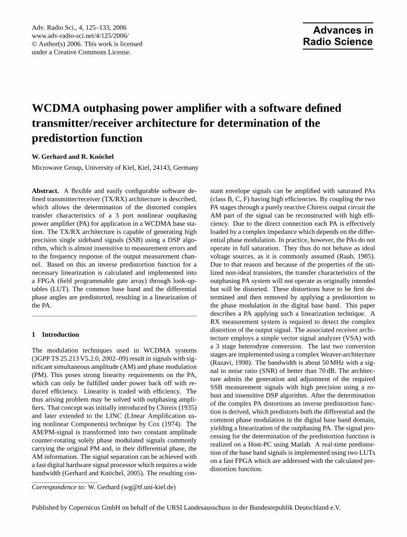
Fig. 1. Implementation of the 24 W outphasing PA.
2 Outphasing PA
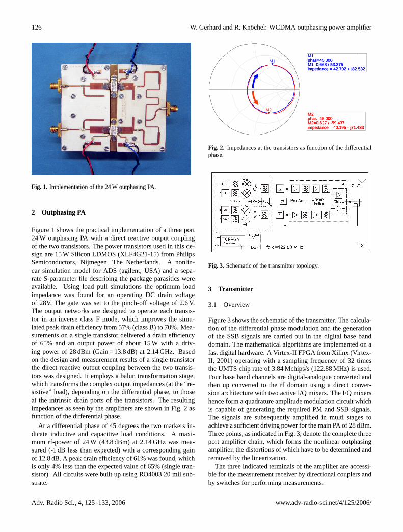
Figure 1 shows the practical implementation of a three port24 W outphasing PA with a direct reactive output couplingof the two transistors. The power transistors used in this de-sign are 15 W Silicon LDMOS (XLF4G21-15) from PhilipsSemiconductors, Nijmegen, The Netherlands. A nonlin-ear simulation model for ADS (agilent, USA) and a sepa-rate S-parameter file describing the package parasitics wereavailable. Using load pull simulations the optimum loadimpedance was found for an operating DC drain voltageof 28V. The gate was set to the pinch-off voltage of 2.6 V.The output networks are designed to operate each transis-tor in an inverse class F mode, which improves the simu-lated peak drain efficiency from 57% (class B) to 70%. Mea-surements on a single transistor delivered a drain efficiencyof 65% and an output power of about 15 W with a driv-ing power of 28 dBm (Gain = 13.8 dB) at 2.14 GHz. Basedon the design and measurement results of a single transistorthe direct reactive output coupling between the two transis-tors was designed. It employs a balun transformation stage,which transforms the complex output impedances (at the “re-sistive” load), depending on the differential phase, to thoseat the intrinsic drain ports of the transistors. The resultingimpedances as seen by the amplifiers are shown in Fig. 2 asfunction of the differential phase.
At a differential phase of 45 degrees the two markers in-dicate inductive and capacitive load conditions. A maxi-mum rf-power of 24 W (43.8 dBm) at 2.14 GHz was mea-sured (-1 dB less than expected) with a corresponding gainof 12.8 dB. A peak drain efficiency of 61% was found, whichis only 4% less than the expected value of 65% (single tran-sistor). All circuits were built up using RO4003 20 mil sub-strate.
2
output coupling between the two transistors was designed. It employs a balun transformation stage, which transforms the complex output impedances (at the “resistive” load), depending on the differential phase, to those at the intrinsic drain ports of the transistors. The resulting impedances as seen by the amplifiers are shown in Fig. 2 as functions of the differential phase.
Fig. 1. Implementation of the 24W outphasing PA. At a differential phase of 45 degrees the two markers indicate inductive and capacitive load conditions. A maximum rf-power of 24W (43.8dBm) at 2.14GHz was measured (-1dB less than expected) with a corresponding gain of 12.8dB. A peak drain efficiency of 61% was found, which is only 4% less than the expected value of 65% (single transistor). All circuits were built up using RO4003 20 mil substrate.
Fig. 2. Impedances at the transistors as functions of the differential phase.
III. TRANSMITTER A. Overview Fig. 3 shows the schematic of the transmitter. The calculation of the differential phase modulation and the generation of the SSB signals are carried out in the digital base band domain. The mathematical algorithms are implemented on a fast digital hardware. A Virtex-II FPGA from Xilinx [7] operating with a sampling frequency of 32 times the UMTS chip rate of
3.84Mchips/s (122.88MHz) is used. Four base band channels are digital-analogue converted and then up converted to the rf domain using a direct conversion architecture with two active I/Q mixers. The I/Q mixers hence form a quadrature amplitude modulation circuit which is capable of generating the required PM and SSB signals. The signals are subsequently amplified in multi stages to achieve a sufficient driving power for the main PA of 28dBm. Three points, as indicated in Fig. 3, denote the complete three port amplifier chain, which forms the nonlinear outphasing amplifier, the distortions of which have to be determined and removed by the linearization.
Fig. 3. Schematic of the transmitter topology. The three indicated terminals of the amplifier are accessible for the measurement receiver by directional couplers and by switches for performing measurements. B. Base Band Implementation The hardware implementation of the digital signal processor on the TX-FPA is shown in Fig. 4. Two pseudo noise bit sources, I and Q, with a chip rate of 3.84Mchips/s are implemented. They are pulse shaped with 2x oversampling (7.68MHz) and then interpolated 16x to a sampling frequency of 122.88MHz employing efficient polyphase filters. With a special CORDIC algorithm the I/Q signals are transformed from their cartesian into the polar representation.
Fig. 4. DSP hardware implementation on the TX FPGA.
M2 phas= M2=0.627 / -59.437 impedance = 40.195 - j71.433
45.000 M2 phas= M2=0.627 / -59.437 impedance = 40.195 - j71.433
45.000
M1 phas= M1=0.668 / 53.375 impedance = 42.702 + j82.532
45.000 M1 phas= M1=0.668 / 53.375 impedance = 42.702 + j82.532
45.000 M1
M2
Fig. 2. Impedances at the transistors as function of the differentialphase.
Fig. 3. Schematic of the transmitter topology.
3 Transmitter
3.1 Overview
Figure 3 shows the schematic of the transmitter. The calcula-tion of the differential phase modulation and the generationof the SSB signals are carried out in the digital base banddomain. The mathematical algorithms are implemented on afast digital hardware. A Virtex-II FPGA from Xilinx (Virtex-II, 2001) operating with a sampling frequency of 32 timesthe UMTS chip rate of 3.84 Mchips/s (122.88 MHz) is used.Four base band channels are digital-analogue converted andthen up converted to the rf domain using a direct conver-sion architecture with two active I/Q mixers. The I/Q mixershence form a quadrature amplitude modulation circuit whichis capable of generating the required PM and SSB signals.The signals are subsequently amplified in multi stages toachieve a sufficient driving power for the main PA of 28 dBm.Three points, as indicated in Fig. 3, denote the complete threeport amplifier chain, which forms the nonlinear outphasingamplifier, the distortions of which have to be determined andremoved by the linearization.
The three indicated terminals of the amplifier are accessi-ble for the measurement receiver by directional couplers andby switches for performing measurements.
Adv. Radio Sci., 4, 125–133, 2006 www.adv-radio-sci.net/4/125/2006/

W. Gerhard and R. Knochel: WCDMA outphasing power amplifier 127
2
output coupling between the two transistors was designed. It employs a balun transformation stage, which transforms the complex output impedances (at the “resistive” load), depending on the differential phase, to those at the intrinsic drain ports of the transistors. The resulting impedances as seen by the amplifiers are shown in Fig. 2 as functions of the differential phase.
Fig. 1. Implementation of the 24W outphasing PA. At a differential phase of 45 degrees the two markers indicate inductive and capacitive load conditions. A maximum rf-power of 24W (43.8dBm) at 2.14GHz was measured (-1dB less than expected) with a corresponding gain of 12.8dB. A peak drain efficiency of 61% was found, which is only 4% less than the expected value of 65% (single transistor). All circuits were built up using RO4003 20 mil substrate.
Fig. 2. Impedances at the transistors as functions of the differential phase.
III. TRANSMITTER A. Overview Fig. 3 shows the schematic of the transmitter. The calculation of the differential phase modulation and the generation of the SSB signals are carried out in the digital base band domain. The mathematical algorithms are implemented on a fast digital hardware. A Virtex-II FPGA from Xilinx [7] operating with a sampling frequency of 32 times the UMTS chip rate of
3.84Mchips/s (122.88MHz) is used. Four base band channels are digital-analogue converted and then up converted to the rf domain using a direct conversion architecture with two active I/Q mixers. The I/Q mixers hence form a quadrature amplitude modulation circuit which is capable of generating the required PM and SSB signals. The signals are subsequently amplified in multi stages to achieve a sufficient driving power for the main PA of 28dBm. Three points, as indicated in Fig. 3, denote the complete three port amplifier chain, which forms the nonlinear outphasing amplifier, the distortions of which have to be determined and removed by the linearization.
Fig. 3. Schematic of the transmitter topology. The three indicated terminals of the amplifier are accessible for the measurement receiver by directional couplers and by switches for performing measurements. B. Base Band Implementation The hardware implementation of the digital signal processor on the TX-FPA is shown in Fig. 4. Two pseudo noise bit sources, I and Q, with a chip rate of 3.84Mchips/s are implemented. They are pulse shaped with 2x oversampling (7.68MHz) and then interpolated 16x to a sampling frequency of 122.88MHz employing efficient polyphase filters. With a special CORDIC algorithm the I/Q signals are transformed from their cartesian into the polar representation.
Fig. 4. DSP hardware implementation on the TX FPGA.
M2 phas= M2=0.627 / -59.437 impedance = 40.195 - j71.433
45.000 M2 phas= M2=0.627 / -59.437 impedance = 40.195 - j71.433
45.000
M1 phas= M1=0.668 / 53.375 impedance = 42.702 + j82.532
45.000 M1 phas= M1=0.668 / 53.375 impedance = 42.702 + j82.532
45.000 M1
M2
Fig. 4. DSP hardware implementation on the TX FPGA.
3.2 Base band implementation
The hardware implementation of the digital signal processoron the TX-FPA is shown in Fig. 4. Two pseudo noise bitsources, I and Q, with a chip rate of 3.84 Mchips/s are im-plemented. They are pulse shaped with 2× oversampling(7.68 MHz) and then interpolated 16× to a sampling fre-quency of 122.88 MHz employing efficient polyphase filters.With a special CORDIC algorithm the I/Q signals are trans-formed from their cartesian into the polar representation.
Thus the envelope and the instantaneous phase informa-tion of the base band signal are determined. LUT1 is usedto transform the envelope to the corresponding differentialphase modulation. Without applying a signal predistortionan arcos() function would be stored and LUT2 would not berequired. In order to linearize the PA transfer characteristicsLUT2 becomes necessary for applying predistortion to thecommon phase (instantaneous base band phase). The LUTsare implemented with a 16× 16 bit resolution, which yields avery high and precise resolution. Four Direct Digital Synthe-sizers (DDS) are implemented. They serve different tasks:
1. In the TX mode the DDSs separate the phase modula-tion into the real and the imaginary part, cos(), sin().Together with the rf QAM up conversion architecturephase modulated constant envelope signals are gener-ated.
2. The DDSs are used as frequency generators to generateSSB test signals for measuring the PA distortions afterthe phase modulation of the DDSs is switched off. Eachchannel can be adjusted in frequency, amplitude (gainblock) and phase with very high precision and SSB sup-pression.
3. The DDSs produce a trigger-signal, after they are startedwell defined at a zero phase, which is used at theRX side for defined phase measurements and syn-chronous repetition of measurements to average the sig-nals, which reduces the measurement errors defined bynoise fluctuations.
With the use of active I/Q mixers a high LO suppressionof -60 dB can be obtained. The signal to noise ratio (SNR)
3
Thus the envelope and the instantaneous phase information of the base band signal are determined. LUT1 is used to transform the envelope to the corresponding differential phase modulation. Without applying a signal predistortion an arcos() function would be stored and LUT2 would not be required. In order to linearize the PA transfer characteristics LUT2 becomes necessary for applying predistortion to the common phase (instantaneous base band phase). The LUTs are implemented with a 16x16 bit resolution, which yields a very high and precise resolution. Four Direct Digital Synthesizers (DDS) are implemented. They serve different tasks:
1. In the TX mode the DDSs separate the phase modulation into the real and the imaginary part, cos(), sin(). Together with the rf QAM up conversion architecture phase modulated constant envelope signals are generated.
2. The DDSs are used as frequency generators to
generate SSB test signals for measuring the PA distortions after the phase modulation of the DDSs is switched off. Each channel can be adjusted in frequency, amplitude (gain block) and phase with very high precision and SSB suppression.
3. The DDSs produce a trigger-signal, after they are
started well defined at a zero phase, which is used at the RX side for defined phase measurements and synchronous repetition of measurements to average the signals, which reduces the measurement errors defined by noise fluctuations.
With the use of active I/Q mixers a high LO suppression of -60dB can be obtained. The signal to noise ratio (SNR) is better than 75dB and distortions like harmonics and intermodulation distortions are suppressed better than 65dB. The designed low phase noise PLL has an rms phase noise of about 0.65°. Fig. 5 shows the double side band (DSB) spectrum plot of one rf branch.
2110 2120 2130 2140 2150 2160 2170-100
-80
-60
-40
-20
freq [MHz ]
am
plit
ud
e [
dB
m]
LSB USB
TX LO
harm .DAC
S/N =75 dB
Fig. 5. TX-DSB-spectrum at 2.14GHz with a base band frequency of 15MHz. Phase noise: 1 KHz offset: -95dBc, rms-phase: 0,65°.
IV. MEASUREMENT RECEIVER A. RX Architecture The schematic of the RX system is shown in Fig. 6. The rf front end of the measurement receiver is designed as a “near zero IF” conversion stage, i.e. a single heterodyne conversion with a low 1. IF. The rf signal is down converted to a IF of 30.72 MHz, which is clk/4. This is done by a second PLL, which is coupled to the same reference clock of 122.88MHz. This allows synchronous operation of all building blocks of the TX/RX system. The theoretical bandwidth of the receiver is clk/2, i.e. about 60MHz. The disadvantage of this RX architecture is the image reject problem, which becomes important if the overall outphasing PA initially is not calibrated. In this situation the PA output spectrum needs a huge frequency bandwidth and an aliasing problem occurs. It will be shown later how this problem can be alleviated.
Fig. 6. Hardware implementation of the wideband measurement receiver. The first IF is amplified twice by voltage controlled gain amplifiers (VGA) with high linearity. It is sampled by an ADC, operating on the system clock. The samples are stored into a FIFO (RX-FPGA) and the further data processing is realized on a Host-PC. To constantly obtain an optimum dynamic range of the ADC the two VGAs are controlled by the RX-FPGA. To reduce the hardware complexity the receiver is designed as a single channel receiver, without an additional reference channel, which is usually implemented if precise phase measurements are required (as vector network analyzer technique). In the present case the phase measurement is based on the concept of a “digital sampling oscilloscope”, where a trigger signal generated by the TX-DDS is used. The disadvantage of this selected architecture is the phase noise of the RX-PLL, which determines the measurement uncertainty. Therefore the PLL requires very low phase noise and averaging in time domain (number of samples) in order to obtain a sufficiently low phase measurement uncertainty. B. Base Band Architecture/Algorithm The base band algorithm of the receiver with the rf front end is shown in Fig. 7. To determine the SSB suppression of the transmitter a Weaver architecture is selected. This kind of
Fig. 5. TX-DSB-spectrum at 2.14 GHz with a base band frequencyof 15 MHz. Phase noise: 1 KHz offset: -95 dBc, rms-phase: 0.65◦.
Fig. 6. Hardware implementation of the wideband measurementreceiver.
is better than 75 dB and distortions like harmonics and in-termodulation distortions are suppressed better than 65 dB.The designed low phase noise PLL has an rms phase noiseof about 0.65◦. Figure 5 shows the double side band (DSB)spectrum plot of one rf branch.
4 Measurement receiver
4.1 RX Architecture
The schematic of the RX system is shown in Fig. 6. The rffront end of the measurement receiver is designed as a “nearzero IF” conversion stage, i.e. a single heterodyne conversionwith a low 1. IF. The rf signal is down converted to an IF of30.72 MHz, which is clk/4. This is done by a second PLL,which is coupled to the same reference clock of 122.88 MHz.This allows synchronous operation of all building blocks ofthe TX/RX system. The theoretical bandwidth of the receiveris clk/2, i.e. about 60 MHz. The disadvantage of this RXarchitecture is the image reject problem, which becomes im-portant if the overall outphasing PA initially is not calibrated.In this situation the PA output spectrum needs a huge fre-quency bandwidth and an aliasing problem occurs. It will beshown later how this problem can be alleviated.
The first IF is amplified twice by voltage controlled gainamplifiers (VGA) with high linearity. It is sampled by an
www.adv-radio-sci.net/4/125/2006/ Adv. Radio Sci., 4, 125–133, 2006

128 W. Gerhard and R. Knochel: WCDMA outphasing power amplifier
Fig. 7. VSA architecture (Heterodyne)with 3 stage conversion, phase mea-surement with a Trigger signal.
ADC, operating on the system clock. The samples are storedinto a FIFO (RX-FPGA) and the further data processing isrealized on a Host-PC. To constantly obtain an optimum dy-namic range of the ADC the two VGAs are controlled by theRX-FPGA. To reduce the hardware complexity the receiveris designed as a single channel receiver, without an additionalreference channel, which is usually implemented if precisephase measurements are required (as vector network ana-lyzer technique). In the present case the phase measurementis based on the concept of a “digital sampling oscilloscope”,where a trigger signal generated by the TX-DDS is used. Thedisadvantage of this selected architecture is the phase noiseof the RX-PLL, which determines the measurement uncer-tainty. Therefore the PLL requires very low phase noise andaveraging in time domain (number of samples) in order toobtain a sufficiently low phase measurement uncertainty.
4.2 Base band architecture/algorithm
The base band algorithm of the receiver with the rf front endis shown in Fig. 7. To determine the SSB suppression ofthe transmitter a Weaver architecture is selected. This kindof signal processing results in separated complex lower andupper sideband information (amplitude, phase) over a band-width of more than 50 MHz.
The fixed digital mixing frequency for the second downconversion is clk/4 (30.72 MHz). The mixing operation canbe realized with an efficient multiplexer instead of perform-ing a multiplication operation. Behind the mixing stage anefficient half band filter (fc = clk/4) is implemented, whichremoves mixing images. The third frequency translation is ahomodyne down conversion. The required mixing frequencyis exactly known from the TX-DDS and a carrier recovery
loop is not required. After the last frequency down conver-sion the average over all RX-samples is performed. The aver-age operation corresponds to a low pass filtering, which im-proves the measurement uncertainty due to rejecting of theAC components, like phase noise and remaining mixing sig-nal components. Furthermore the implementation of a fre-quency adaptive low pass filter after the third mixing stage iscircumvented.
4.3 RX-performance
For the TX and RX the PLLs were designed with a fixed fre-quency and coupled to the same system clock reference. Thephase noise at 1 KHz offset was measured as -95 dBc at a car-rier frequency of 2.14 GHz. This corresponds to a rms phasedeviation of 0.65◦. The peak-peak phase uncertainty canbe approximated with a Gaussian noise distribution, whichgives a phase uncertainty of about 4.5◦ (7× 0.65◦) for onemeasurement sample. Figures 8 and 9 plot the measuredmaximum amplitude and phase uncertainties as functions ofthe number of samples used for the averaging operation. Itcan be deduced, that by increasing of the number of samplesboth uncertainties will tend to approach a value of zero, asexpected. Practically 8192–16384 samples are used. Thisresults in a satisfying amplitude and phase measurement un-certainty. Therefore the RX-FIFO depth requirements can bedefined to have a size of about 16384 samples using a 14 bitamplitude resolution (14 bit ADC).
Figure 10 plots the investigation of nonlinear properties ofthe wideband receiver with a 2 tone test signal, measured inthe digital domain. The key parameter like IMD3, S/N andharmonics can be deduced. The nonlinear performance dataare summarized in Table 1. The amplitude/phase frequency
Adv. Radio Sci., 4, 125–133, 2006 www.adv-radio-sci.net/4/125/2006/

W. Gerhard and R. Knochel: WCDMA outphasing power amplifier 129
0.5 1 1.5 2x 10 4
0
0.02
0.04
0.06
0.08
0.1
samples
max
. am
plitu
de u
ncer
tain
ty [d
B] 1 MHz30 MHz60 MHz
o
o
x
x
0.5 1 1.5 2x 10 4
0
0.02
0.04
0.06
0.08
0.1
samples
max
. am
plitu
de u
ncer
tain
ty [d
B] 1 MHz30 MHz60 MHz
o
o
x
x
Fig. 8. Amplitude uncertainty vs. number of samples.
0.5 1 1.5 2x 10
4
0
1
2
3
4
samples
max
. pha
se u
ncer
tain
ty [d
eg] 1 MHz
30 MHz60 MHz
ox
o
x
0.5 1 1.5 2x 10
4
0
1
2
3
4
samples
max
. pha
se u
ncer
tain
ty [d
eg] 1 MHz
30 MHz60 MHz
ox
o
x
Fig. 9. Phase uncertainty vs. number of samples.
Table 1.Pin for ADC drive, power control loop -16 . . . -32 dBm
1 dB bandwidth > 50 MHz
signal / harmonics, 2. order > 65 dB
signal / harmonics, 3. order > 65 dB
signal / IM3, spurious > 65 dB
signal / noise > 70 dB
within of 60 dB signal dynamic: < 0.5 dBampl. uncertainty, pk-pk
phase uncertainty, pk-pk < 1◦
response of the receiver can be corrected with an equaliza-tion algorithm. The amplitude frequency response is mea-sured and modelled by means of an FIR filter. Then an in-verse function, again a FIR filter, can be implemented equal-
4
signal processing results in separated complex lower and upper sideband information (amplitude, phase) over a bandwidth of more than 50MHz.
Fig. 7. VSA architecture (Heterodyne) with 3 stage conversion, phase measurement with a Trigger signal. The fixed digital mixing frequency for the second down conversion is clk/4 (30.72MHz). The mixing operation can be realized with an efficient multiplexer instead of performing a multiplication operation. Behind the mixing stage an efficient half band filter (fc=clk/4) is implemented, which removes mixing images. The third frequency translation is a homodyne down conversion. The required mixing frequency is exactly known from the TX-DDS and a carrier recovery loop is not required. After the last frequency down conversion the average over all RX-samples is performed. The average operation corresponds to a low pass filtering, which improves the measurement uncertainty due to rejecting of the AC components, like phase noise and remaining mixing signal components. Furthermore the implementation of a frequency adaptive low pass filter after the third mixing stage is circumvented. C. RX-Performance For the TX and RX the PLLs were designed with a fixed frequency and coupled to the same system clock reference. The phase noise at 1KHz offset was measured as -95dBc at a carrier frequency of 2.14GHz. This corresponds to an rms phase deviation of 0.65°. The peak-peak phase uncertainty can be approximated with a Gaussian noise distribution, which gives a phase uncertainty of about 4.5° (7x 0.65°) for one measurement sample. Fig. 8 and Fig. 9 plots the measured maximum amplitude and phase uncertainties as functions of the number of samples used for the averaging operation. It can be deduced, that by increasing of the number of samples both uncertainties will tend to approach a value of zero, as expected. Practically 8192-16384 samples are used. This results in a satisfying amplitude and phase measurement uncertainty. Therefore the RX-FIFO depth requirements can
be defined to have a size of about 16384 samples using a 14bit amplitude resolution (14bit ADC).
Fig. 8. Amplitude uncertainty vs. number of samples.
Fig. 9. Phase uncertainty vs. number of samples.
Fig. 10. RX 2 tone performance, time domain and frequency spectrum representation. Fig. 10 plots the investigation of nonlinear properties of the wideband receiver with a 2 tone test signal, measured in the
Fig. 10. RX 2 tone performance, time domain and frequency spec-trum representation.
5
Table I
Pin for ADC drive, power control loop
-16 … -32 dBm
1dB bandwidth > 50 MHz signal / harmonics, 2. order > 65 dB signal / harmonics, 3. order > 65 dB signal / IM3, spurious > 65 dB signal / noise > 70 dB within of 60dB signal dynamic: ampl. uncertainty, pk-pk
< 0.5 dB phase uncertainty, pk-pk < 1° digital domain. The key parameter like IMD3, S/N and harmonics can be deduced. The nonlinear performance data are summarized in Table I. The amplitude/phase frequency response of the receiver can be corrected with an equalization algorithm. The amplitude frequency response is measured and modelled by means of an FIR filter. Then an inverse function, again a FIR Filter, can be implemented equalizing the amplitude frequency response. The FIR filter has the advantage of having absolute stability and a linear phase response, but the required order of the filter can increase dramatically. Furthermore the equalization accuracy is limited. Fig. 11 shows the amplitude frequency response before and after equalization over a bandwidth of about 50MHz. In addition group delay distortions mainly introduced by analogue filters can be compensated with all-pass networks.
10 20 30 40 50
-0.6
-0.2
0.2
freq [MHz]
am
plit
ud
e [
dB
]
10 20 30 40 50-0.8
-0.6
-0.4
-0.2
0
0.2
freq [MHz]
am
plit
ud
e d
B
Fig. 11. Amplitude response of the RX VSA before and after channel equalization.
V. TX SINGLE-SIDEBAND-SUPPRESSION (SBS) ALGORITHM
A. General Due to the amplitude/phase frequency response of the directional couplers as well as the subsequent circuitry (e.g. switches) the measurement signal will be falsified. A precise adjustment of the SSB signals will not be possible. It is, however, possible to determine complex values for re- adjustment of the SSB signal by applying an analytical approach which requires the measurement of the SSB suppression (SBS) only. Then the amplitude and phase balance can be obtained by adjusting the TX-DDS. With this algorithmic approach the SBS virtually obtains independency of the complex frequency response of the measurement circuit and measurement accuracy. The measurement error, which may be expressed through a possible amplitude deviation between the two SSB signals (LSB, USB) at their two frequencies, defines the maximum possible adjustment uncertainty. As an example, if an amplitude deviation (introduced by the measurement circuit) between the LSB and USB signal of 3dB occurs and the algorithm tries to adjust the SBS to be -70dB, then the SBS can only achieve -67dB as a worst case, that is 3dB less than the target value. This 3dB is already a quite large variance in the amplitude frequency response of practical circuits, but the impact of this variance to the resulting SBS is quite small. Furthermore this algorithm does not depend upon the phase/frequency response. Knowledge of the phases of the LSB and USB signals is also not required. As a consequence the technical requirements to be put on the coupling circuitry of the measurement circuit can be advantageously reduced. B. SBS-Algorithm The algorithm is demonstrated in Fig. 12 with some simplification. It can be observed, that e.g. -60dB SBS requires the amplitude error to be less than 0.1dB and the phase error to be less than 0.6°. The idea behind the SSB algorithm is to determine the absolute complex operating point first. This corresponds to the actual SBS (I). This is achieved by applying a well defined operating point deviation through adjustment of the TX-DDS. To succeed, two scalar measurements of the SBS (I, III) and a well defined phase adjustment at the TX-DDS (III) are required. Four solution quadrants exist. As a first step the channel having the lower power will be detected. This results in a simplification to two solution quadrants on the right side. The initial SBS (I) is measured. Then a well defined change of the phase in one channel via TX-DDS is applied. To estimate the phase step the corresponding maximum phase
Fig. 11. Amplitude-frequency response of the RX VSA before andafter channel equalization.
izing the amplitude frequency response. The FIR filter hasthe advantage of having absolute stability and a linear phaseresponse, but the required order of the filter can increase dra-matically. Furthermore the equalization accuracy is limited.Figure 11 shows the amplitude frequency response beforeand after equalization over a bandwidth of about 50 MHz. Inaddition group delay distortions mainly introduced by ana-logue filters can be compensated with all-pass networks.
www.adv-radio-sci.net/4/125/2006/ Adv. Radio Sci., 4, 125–133, 2006

130 W. Gerhard and R. Knochel: WCDMA outphasing power amplifier
6
0 0.05 0.1 0.15 0.2 0.25 0.30
0.5
1
1.5
2
gain error ∆A [dB]
phas
e er
ror ∆
Φ [
degr
ee]
SBS1(∆φ1, ∆A)
SBS2(∆φ2
, ∆A)
∆φ1max
∆A=const.∆φ2=∆φ1-∆φ1max/3
-50
-52
-54
-56
-58
-60-62
-64
I
III
II
IV
Fig 12. SBS algorithm with amplitude- and phase dependency. error ∆φ1max (II) is calculated from:
( )
( )
2 2
1max
1 1arccos
2 1
SBS
SBSφ
⋅ + ∆Α −∆Α −∆ =
⋅∆Α⋅ + (1)
with ∆A = 1. A phase change by the well defined value of ∆φ1max/3 is now applied to of one of the TX-DDSs and a second measurement of the SBS (III) is carried out. The phase step is empirically adjusted to 1/3, but can be chosen freely. From the two SBS measurements two equations with two unknowns can be derived
( )( )
21,2
1,2 21,2
1 2 cosSBS
1 2 cos
φ
φ
+ ∆Α ∆ + ∆Α=
− ∆Α ∆ + ∆Α. (2)
From eq.(2) a bi-quadratic polynomial equation is obtained
4 2 1 0q∆Α + ∆Α + = , (3)
which delivers two positive solutions for ∆A (Negative values for ∆A are not meaningful). The two solutions are reciprocal to eachother. The one, which is less than 1, is kept, because the solution quadrant is known. The following equation has to be solved
( )( )
( )( )
2 2 2
2 2 2
2 2 2
2 2 2
2 sin 1
2 cos
2 sin1 1
2 cos
s
s
s
s
T R
R S T RST
T R
R S T RST
φ
φ
φ
φ
∆− + −
+ − ∆∆Α =
∆− −
+ − ∆
with
( ) ( ) 1max12 2
1
SBS 11 SBS , SBS 1 , , SBS 1 3sR S T φφ ∆+= + = − = ∆ =
−
(4) The channel having the higher power will now be multiplied with the solved ∆A. The corresponding phase ∆φ1 can be determined from eq.(5):
( )( )( )
22
12
1 SBS 1arccos
2 1 SBS sφ φ
∆Α + −∆ = − ∆
Α + . (5)
Finally the phase of one channel can be corrected with the TX-DDS and the SBS becomes perfectly adjusted (IV). Due to measurement and calculation inaccuracies the algorithm has to be repeated iteratively. If a SBS < -70dB is achieved the iteration loop is stopped. Usually only a few iteration cycles are necessary.
VI. PA DISTORTION AND PREDISTORTION
A. PA Transfer Characteristics Fig. 13 shows a simulation plot of the output power behaviour and the common phase distortions of the outphasing PA as functions of the differential phase (simulations with ADS, agilent). The output power drops down more rapidly than expected and the common phase does not stay constant, which is caused by the directive output coupling of the power transistors and their behaviour as real voltage sources in saturation. It also can be deduced, that two possible solution areas exist to the left and right to the location of the zero. This is interesting, because the transfer characteristics as well as the related PA efficiencies are not symmetric. Hence characteristic which suits best (left or right) should finally be chosen with respect to the predistortion algorithm. The presence of a signal distortion can already deduced from the simulation results. Therefore the evaluation of the PA transfer characteristics is necessary. It was and should be determined through practical in-circuit measurements. During the practical measurements the SSB signals were generated first and adjusted. Then the
Fig. 12. SBS algorithm with amplitude- and phase dependency.
5 TX single-sideband-suppression (SBS) algorithm
5.1 General
Due to the amplitude/phase frequency response of the di-rectional couplers as well as the subsequent circuitry (e.g.switches) the measurement signal will be falsified. A pre-cise adjustment of the SSB signals will not be possible. Itis, however, possible to determine complex values for re-adjustment of the SSB signal by applying an analytical ap-proach, which requires the measurement of the SSB suppres-sion (SBS) only. Then the amplitude and phase balance canbe obtained by adjusting the TX-DDS. With this algorith-mic approach the SBS virtually obtains independency of thecomplex frequency response of the measurement circuit andmeasurement accuracy. The measurement error, which maybe expressed through a possible amplitude deviation betweenthe two SSB signals (LSB, USB) at their two frequencies,defines the maximum possible adjustment uncertainty. As anexample, if an amplitude deviation (introduced by the mea-surement circuit) between the LSB and USB signal of 3 dBoccurs and the algorithm tries to adjust the SBS to be -70 dB,then the SBS can only achieve -67 dB as a worst case, that is3 dB less than the target value. This 3 dB is already a quitelarge variance in the amplitude frequency response of prac-tical circuits, but the impact of this variance to the resultingSBS is quite small. Furthermore this algorithm does not de-pend upon the phase/frequency response. Knowledge of thephases of the LSB and USB signals is also not required. Asa consequence the technical requirements to be put on thecoupling circuitry of the measurement circuit can be advan-tageously reduced.
5.2 SBS-algorithm
The algorithm is demonstrated in Fig. 12 with some simplifi-cation. It can be observed, that e.g. -60 dB SBS requires theamplitude error to be less than 0.1 dB and the phase error tobe less than 0.6◦. The idea behind the SSB algorithm is to de-termine the absolute complex operating point first. This cor-responds to the actual SBS (I). This is achieved by applyinga well defined operating point deviation through adjustmentof the TX-DDS. To succeed, two scalar measurements of theSBS (I, III) and a well defined phase adjustment at the TX-DDS (III) are required. Four solution quadrants exist. As afirst step the channel having the lower power will be detected.This results in a simplification to two solution quadrants onthe right side. The initial SBS (I) is measured. Then a welldefined change of the phase in one channel via TX-DDS isapplied. To estimate the phase step the corresponding maxi-mum phase error1φ1max (II) is calculated from:
1φ1 max = arccos
(SBS ·
(1 + 1A2
)− 1A2
− 1
2 · 1A · (1 + SBS)
)(1)
with 1A = 1.A phase change by the well defined value of1φ1max /3
is now applied to of one of the TX-DDSs and a second mea-surement of the SBS (III) is carried out. The phase step is em-pirically adjusted to 1/3, but can be chosen freely. From thetwo SBS measurements two equations with two unknownscan be derived
SBS1,2 =1 + 21A cos
(1φ1,2
)+ 1A2
1 − 21A cos(1φ1,2
)+ 1A2
. (2)
From Eq. (2) a bi-quadratic polynomial equation is obtained
1A4+ q1A2
+ 1 = 0, (3)
which delivers two positive solutions for1A (negative val-ues for1A are not meaningful). The two solutions are re-ciprocal to eachother. The one, which is less than 1, is kept,because the solution quadrant is known.
The following equation has to be solved
1A =
√√√√√√√√−1 +
2T 2R2 sin2(1φs )
R2+S2T 2−2RST cos(1φs )
−
√(1 −
2T 2R2 sin2(1φs )
(R2+S2T 2−2RST cos(1φs ))
)− 1
with
R = (1 + SBS2) , S = (SBS2 − 1) ,
T =SBS1 + 1
SBS1 − 1, 1φs =
1φ1 max
3(4)
The channel having the higher power will now be multi-plied with the solved1A. The corresponding phase1φ1 canbe determined from Eq. (5):
1φ1 = arccos
((1A2
+ 1)(SBS2 − 1)
2A (1 + SBS2)
)− 1φs . (5)
Adv. Radio Sci., 4, 125–133, 2006 www.adv-radio-sci.net/4/125/2006/

W. Gerhard and R. Knochel: WCDMA outphasing power amplifier 131
-70 -50 -30 -10 10 30 50 70-90 90
-40
-30
-20
-10
0
differential phase [deg]
outp
utpo
wer
[dB
]
ideal
PA
-70 -50 -30 -10 10 30 50 70-90 90
-40
-30
-20
-10
0
differential phase [deg]
outp
utpo
wer
[dB
]
ideal
PA
differential phase [deg]
com
mon
phas
e[d
eg]
-70 -50 -30 -10 10 30 50 70-90 90
-60-202060
100
140180
PA
ideal
differential phase [deg]
com
mon
phas
e[d
eg]
-70 -50 -30 -10 10 30 50 70-90 90
-60-202060
100
140180
PA
ideal
Fig. 13. Simulated distortions of the outphasing PA at 2.14 GHz,(a) output power,(b) output common phase vs. differential phase.
Finally the phase of one channel can be corrected with theTX-DDS and the SBS becomes perfectly adjusted (IV).
Due to measurement and calculation inaccuracies the al-gorithm has to be repeated iteratively. If a SBS< −70 dBis achieved the iteration loop is stopped. Usually only a fewiteration cycles are necessary.
6 PA distortion and predistortion
6.1 PA transfer characteristics
Figure 13 shows a simulation plot of the output power be-haviour and the common phase distortions of the outphasingPA as functions of the differential phase (simulations withADS, agilent). The output power drops down more rapidlythan expected and the common phase does not stay constant,which is caused by the directive output coupling of the powertransistors and their behaviour as real voltage sources in sat-uration. It also can be deduced, that two possible solution ar-eas exist to the left and right to the location of the zero. Thisis interesting, because the transfer characteristics as well asthe related PA efficiencies are not symmetric. Hence charac-teristic which suits best (left or right) should finally be chosenwith respect to the predistortion algorithm. The presence ofa signal distortion can already deduced from the simulationresults. Therefore the evaluation of the PA transfer character-istics is necessary. It was and should be determined through
-90 -70 -50 -30 -10 10 30 50 70 90-35
-30
-25
-20
-15
-10
-5
0
--1 MHz
-10 MHz+10 MHz
outp
utpo
wer
[dB
]
differential phase [deg]-90 -70 -50 -30 -10 10 30 50 70 90
-35
-30
-25
-20
-15
-10
-5
0
--1 MHz
-10 MHz+10 MHz
outp
utpo
wer
[dB
]
differential phase [deg]
differential phase [deg]-90 -70 -50 -30 -10 10 30 50 70 90
-50
0
50
100
150
200
-10 MHz+10 MHz
-1 MHzcom
mon
phas
e[d
eg]
differential phase [deg]-90 -70 -50 -30 -10 10 30 50 70 90
-50
0
50
100
150
200
-10 MHz+10 MHz
-1 MHzcom
mon
phas
e[d
eg]
Fig. 14. Distortions of the outphasing PA at 2.14 GHz,(a) out-put power,(b) output common phase vs. differential phase and fre-quency offset.
practical in-circuit measurements. During the practical mea-surements the SSB signals were generated first and adjusted.Then the differential phase between the 2 SSB carriers wasswept and the output power and common phase were mea-sured. Figure 14 plots the measured characteristics. The fre-quency offset was also varied.
Furthermore, for defining the starting point of a predis-tortion, a reference point has to be devised as the absolutedifferential phase angle for maximum or minimum power. InFigs. 13 and 14 the derived characteristics are already nor-malized to this point and represent relative curves. The prac-tical measurements were performed with an angle resolutionof 1◦. From the measured amplitude curve the zero depth canbe deduced. It is approximately -30 dB, which is good prac-tical value. A perfect vector cancellation and a perfect zerocan not be obtained due to asymmetries of the practical PAs.If the measured data are compared with the simulated data,a quite fair agreement between both can be deduced. Thedifferential phase for the -10 dB output power back off canbe determined as -30◦ for both cases. The output phase ver-sus differential phase is decreasing on the left and increasing
www.adv-radio-sci.net/4/125/2006/ Adv. Radio Sci., 4, 125–133, 2006
132 W. Gerhard and R. Knochel: WCDMA outphasing power amplifier
8
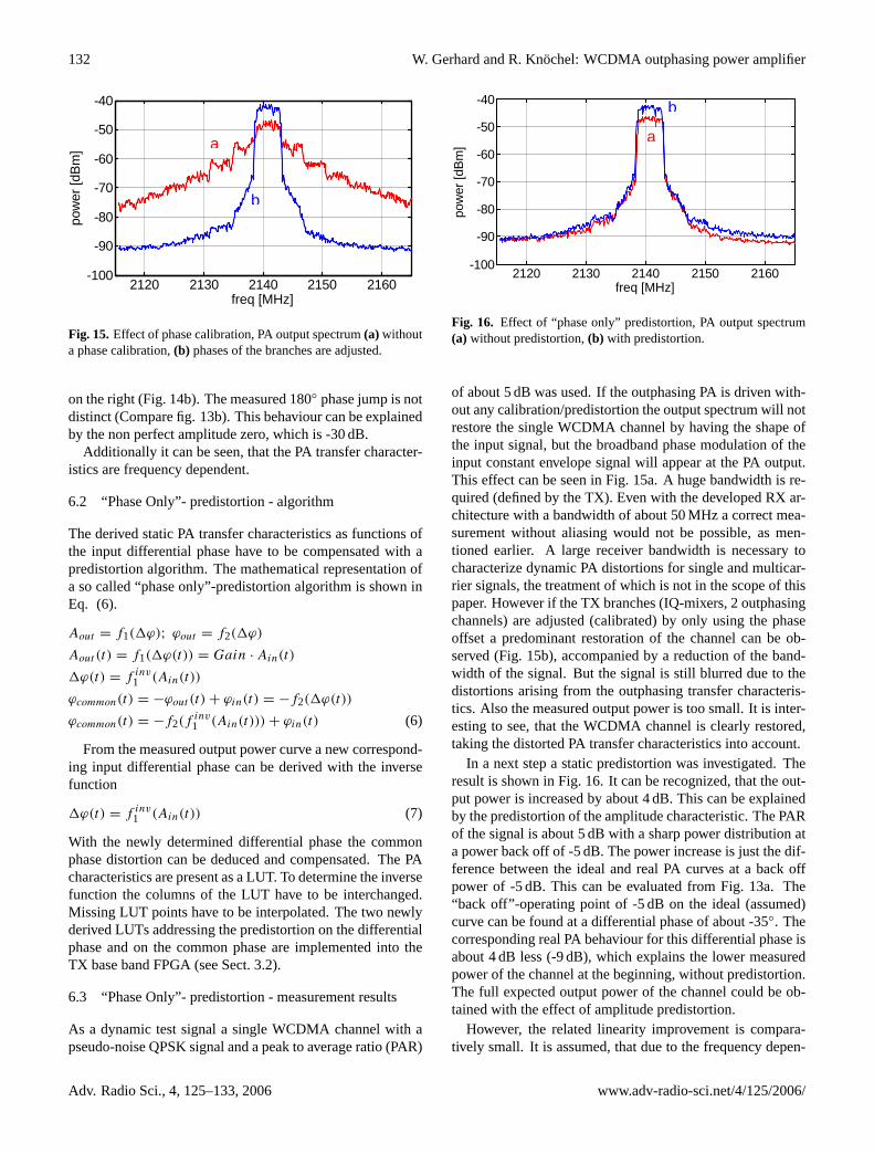
function the columns of the LUT have to be interchanged. Missing LUT points have to be interpolated. The two newly derived LUTs addressing the predistortion on the differential phase and on the common phase are implemented into the TX base band FPGA (see chapter III.B). C. “Phase Only”- Predistortion - Measurement Results As a dynamic test signal a single WCDMA channel with a pseudo-noise QPSK signal and a peak to average ratio (PAR) of about 5dB was used. If the outphasing PA is driven without any calibration/predistortion the output spectrum will not restore the single WCDMA channel by having the shape of the input signal, but the broadband phase modulation of the input constant envelope signal will appear at the PA output. This effect can be seen in Fig.15a. A huge bandwidth is required (defined by the TX). Even with the developed RX architecture with a bandwidth of about 50MHz a correct measurement without aliasing would not be possible, as mentioned earlier. A large receiver bandwidth is necessary to characterize dynamic PA distortions for single and multicarrier signals, the treatment of which is not in the scope of this paper. However if the TX branches (IQ-mixers, 2 outphasing channels) are adjusted (calibrated) by only using the phase offset a predominant restoration of the channel can be observed (Fig.15b), accompanied by a reduction the bandwidth of the signal. But the signal is still blurred due to the distortions arising from the outphasing transfer characteristics. Also the measured output power is too small. It is interesting to see, that the WCDMA channel is clearly restored, taking the distorted PA transfer characteristics into account.
Fig. 15. Effect of phase calibration, PA output spectrum a) without a phase calibration, b) phases of the branches are adjusted. In a next step a static predistortion was investigated. The result is shown in Fig. 16. It can be recognized, that the output power is increased by about 4dB. This can be explained by the predistortion of the amplitude characteristic. The PAR of the signal is about 5dB with a sharp power distribution at a power
back off of -5dB. The power increase is just the difference between the ideal and real PA curves at a back off power of -5dB. This can be evaluated from Fig. 13a. The “back off”-operating point of -5dB on the ideal (assumed) curve can be found at a differential phase of about -35°. The corresponding real PA behaviour for this differential phase is about 4dB less (-9dB), which explains the lower measured power of the channel at the beginning, without predistortion. The full expected output power of the channel could be obtained with the effect of amplitude predistortion.
Fig. 16. Effect of “phase only” predistortion, PA output spectrum a) without predistortion, b) with predistortion. However, the related linearity improvement is comparatively small. It is assumed, that due to the frequency dependence of the PA distortions and the wide bandwidth requirement of the outphasing approach a perfect vector cancellation can not be obtained with a static (one frequency) distortion characterisation. Therefore dynamic techniques, considering the whole outphasing bandwidth has to be developed and applied, which is in the scope for further research.
VII. CONCLUSION
A powerful, configurable, software defined transmitter/ receiver architecture is proposed for application with PAs using the outphasing concept. Such an approach is interesting, because it has the potential of facilitating the trade off between linearity and efficiency of PAs in WCDMA base stations. A complex TX/RX system is necessary for providing the differential phase modulation in order to drive the outphasing 3 port PA, to determine the system distortions and to apply a calibration and a predistortion algorithm. An almost error-insensitive and efficient DSP algorithm is described, which enables the generation of precise SSB signals. SSB signals (CW) are used for measuring the distorted complex transfer characteristics. The proposed vector receiver architecture offers a simple solution having a large bandwidth. Phase measurements are performed with a Trigger signal generation
2120 2130 2140 2150 2160-100
-90
-80
-70
-60
-50
-40
freq [MHz]
pow
er [d
Bm
] a
b
2120 2130 2140 2150 2160-100
-90
-80
-70
-60
-50
-40
freq [MHz]
pow
er [d
Bm
]
a b
Fig. 15.Effect of phase calibration, PA output spectrum(a) withouta phase calibration,(b) phases of the branches are adjusted.
on the right (Fig. 14b). The measured 180◦ phase jump is notdistinct (Compare fig. 13b). This behaviour can be explainedby the non perfect amplitude zero, which is -30 dB.
Additionally it can be seen, that the PA transfer character-istics are frequency dependent.
6.2 “Phase Only”- predistortion - algorithm
The derived static PA transfer characteristics as functions ofthe input differential phase have to be compensated with apredistortion algorithm. The mathematical representation ofa so called “phase only”-predistortion algorithm is shown inEq. (6).
Aout = f1(1ϕ); ϕout = f2(1ϕ)
Aout (t) = f1(1ϕ(t)) = Gain · Ain(t)
1ϕ(t) = f inv1 (Ain(t))
ϕcommon(t) = −ϕout (t) + ϕin(t) = −f2(1ϕ(t))
ϕcommon(t) = −f2(finv1 (Ain(t))) + ϕin(t) (6)
From the measured output power curve a new correspond-ing input differential phase can be derived with the inversefunction
1ϕ(t) = f inv1 (Ain(t)) (7)
With the newly determined differential phase the commonphase distortion can be deduced and compensated. The PAcharacteristics are present as a LUT. To determine the inversefunction the columns of the LUT have to be interchanged.Missing LUT points have to be interpolated. The two newlyderived LUTs addressing the predistortion on the differentialphase and on the common phase are implemented into theTX base band FPGA (see Sect. 3.2).
6.3 “Phase Only”- predistortion - measurement results
As a dynamic test signal a single WCDMA channel with apseudo-noise QPSK signal and a peak to average ratio (PAR)
8
function the columns of the LUT have to be interchanged. Missing LUT points have to be interpolated. The two newly derived LUTs addressing the predistortion on the differential phase and on the common phase are implemented into the TX base band FPGA (see chapter III.B). C. “Phase Only”- Predistortion - Measurement Results As a dynamic test signal a single WCDMA channel with a pseudo-noise QPSK signal and a peak to average ratio (PAR) of about 5dB was used. If the outphasing PA is driven without any calibration/predistortion the output spectrum will not restore the single WCDMA channel by having the shape of the input signal, but the broadband phase modulation of the input constant envelope signal will appear at the PA output. This effect can be seen in Fig.15a. A huge bandwidth is required (defined by the TX). Even with the developed RX architecture with a bandwidth of about 50MHz a correct measurement without aliasing would not be possible, as mentioned earlier. A large receiver bandwidth is necessary to characterize dynamic PA distortions for single and multicarrier signals, the treatment of which is not in the scope of this paper. However if the TX branches (IQ-mixers, 2 outphasing channels) are adjusted (calibrated) by only using the phase offset a predominant restoration of the channel can be observed (Fig.15b), accompanied by a reduction the bandwidth of the signal. But the signal is still blurred due to the distortions arising from the outphasing transfer characteristics. Also the measured output power is too small. It is interesting to see, that the WCDMA channel is clearly restored, taking the distorted PA transfer characteristics into account.
Fig. 15. Effect of phase calibration, PA output spectrum a) without a phase calibration, b) phases of the branches are adjusted. In a next step a static predistortion was investigated. The result is shown in Fig. 16. It can be recognized, that the output power is increased by about 4dB. This can be explained by the predistortion of the amplitude characteristic. The PAR of the signal is about 5dB with a sharp power distribution at a power
back off of -5dB. The power increase is just the difference between the ideal and real PA curves at a back off power of -5dB. This can be evaluated from Fig. 13a. The “back off”-operating point of -5dB on the ideal (assumed) curve can be found at a differential phase of about -35°. The corresponding real PA behaviour for this differential phase is about 4dB less (-9dB), which explains the lower measured power of the channel at the beginning, without predistortion. The full expected output power of the channel could be obtained with the effect of amplitude predistortion.
Fig. 16. Effect of “phase only” predistortion, PA output spectrum a) without predistortion, b) with predistortion. However, the related linearity improvement is comparatively small. It is assumed, that due to the frequency dependence of the PA distortions and the wide bandwidth requirement of the outphasing approach a perfect vector cancellation can not be obtained with a static (one frequency) distortion characterisation. Therefore dynamic techniques, considering the whole outphasing bandwidth has to be developed and applied, which is in the scope for further research.
VII. CONCLUSION
A powerful, configurable, software defined transmitter/ receiver architecture is proposed for application with PAs using the outphasing concept. Such an approach is interesting, because it has the potential of facilitating the trade off between linearity and efficiency of PAs in WCDMA base stations. A complex TX/RX system is necessary for providing the differential phase modulation in order to drive the outphasing 3 port PA, to determine the system distortions and to apply a calibration and a predistortion algorithm. An almost error-insensitive and efficient DSP algorithm is described, which enables the generation of precise SSB signals. SSB signals (CW) are used for measuring the distorted complex transfer characteristics. The proposed vector receiver architecture offers a simple solution having a large bandwidth. Phase measurements are performed with a Trigger signal generation
2120 2130 2140 2150 2160-100
-90
-80
-70
-60
-50
-40
freq [MHz]
pow
er [d
Bm
] a
b
2120 2130 2140 2150 2160-100
-90
-80
-70
-60
-50
-40
freq [MHz]
pow
er [d
Bm
]
a b
Fig. 16. Effect of “phase only” predistortion, PA output spectrum(a) without predistortion,(b) with predistortion.
of about 5 dB was used. If the outphasing PA is driven with-out any calibration/predistortion the output spectrum will notrestore the single WCDMA channel by having the shape ofthe input signal, but the broadband phase modulation of theinput constant envelope signal will appear at the PA output.This effect can be seen in Fig. 15a. A huge bandwidth is re-quired (defined by the TX). Even with the developed RX ar-chitecture with a bandwidth of about 50 MHz a correct mea-surement without aliasing would not be possible, as men-tioned earlier. A large receiver bandwidth is necessary tocharacterize dynamic PA distortions for single and multicar-rier signals, the treatment of which is not in the scope of thispaper. However if the TX branches (IQ-mixers, 2 outphasingchannels) are adjusted (calibrated) by only using the phaseoffset a predominant restoration of the channel can be ob-served (Fig. 15b), accompanied by a reduction of the band-width of the signal. But the signal is still blurred due to thedistortions arising from the outphasing transfer characteris-tics. Also the measured output power is too small. It is inter-esting to see, that the WCDMA channel is clearly restored,taking the distorted PA transfer characteristics into account.
In a next step a static predistortion was investigated. Theresult is shown in Fig. 16. It can be recognized, that the out-put power is increased by about 4 dB. This can be explainedby the predistortion of the amplitude characteristic. The PARof the signal is about 5 dB with a sharp power distribution ata power back off of -5 dB. The power increase is just the dif-ference between the ideal and real PA curves at a back offpower of -5 dB. This can be evaluated from Fig. 13a. The“back off”-operating point of -5 dB on the ideal (assumed)curve can be found at a differential phase of about -35◦. Thecorresponding real PA behaviour for this differential phase isabout 4 dB less (-9 dB), which explains the lower measuredpower of the channel at the beginning, without predistortion.The full expected output power of the channel could be ob-tained with the effect of amplitude predistortion.
However, the related linearity improvement is compara-tively small. It is assumed, that due to the frequency depen-
Adv. Radio Sci., 4, 125–133, 2006 www.adv-radio-sci.net/4/125/2006/

W. Gerhard and R. Knochel: WCDMA outphasing power amplifier 133
dence of the PA distortions and the wide bandwidth require-ment of the outphasing approach a perfect vector cancellationcan not be obtained with a static (one frequency) distortioncharacterisation. Therefore dynamic techniques, consideringthe whole outphasing bandwidth has to be developed and ap-plied, which is in the scope for further research.
7 Conclusion
A powerful, configurable, software defined transmitter/ re-ceiver architecture is proposed for application with PAs usingthe outphasing concept. Such an approach is interesting, be-cause it has the potential of facilitating the trade off betweenlinearity and efficiency of PAs in WCDMA base stations. Acomplex TX/RX system is necessary for providing the dif-ferential phase modulation in order to drive the outphasing3 port PA, to determine the system distortions and to applya calibration and a predistortion algorithm. An almost error-insensitive and efficient DSP algorithm is described, whichenables the generation of precise SSB signals. SSB signals(CW) are used for measuring the distorted complex transfercharacteristics. The proposed vector receiver architecture of-fers a simple solution having a large bandwidth. Phase mea-surements are performed with a Trigger signal generation ofthe TX-DDS and an averaging operation to reduce measure-
ment uncertainties. The measured complex transfer charac-teristics are confirming the simulation results. A predistor-tion algorithm based on the static distortion characterisationwas derived and implemented into a TX-FPGA. Further sub-ject of research will be the development and application ofdynamic (broadband) distortion characterisation for furtherlinearity improvement.
References
3GPP TS 25.213 V5.2.0 (2002-09): Spreading and modulation(FDD), available: http://www.3gpp.org.
Chireix, H.: High power outphasing modulation, Pro. IRE, 23,1370–1392, 1935.
Cox, D. C.: Linear Amplification with Nonlinear Components,IEEE Trans. on Commun., 1942–1945, 1974.
Gerhard, W. and Knochel, R.: LINC Digital Component Separatorfor Single and Multicarrier W-CDMA Signals, IEEE Trans. onMTT, 53, 274–282, 2005.
Raab, F. H.: Efficiency of outphasing power-amplifier systems,IEEE Trans. on Commun., 33, 1094–1099, 1985.
Razavi, B.: RF Microelectronics, Prentice-Hall. INC., 1998Virtex-II 1.5V field-programmable gate arrays, Xilinx
datasheet, Xilinx Inc., San Jose, CA, 2001, available:http://www.xilinx.com.
www.adv-radio-sci.net/4/125/2006/ Adv. Radio Sci., 4, 125–133, 2006