Embed Size (px)
Citation preview
1
Outphasing Class-E Power Amplifiers: FromTheory to Back-off Efficiency Improvement
Ali Ghahremani, Student Member, IEEE, Anne-Johan Annema, Member, IEEE andBram Nauta, Fellow, IEEE
Abstract—This paper presents an analysis of outphasing class-E Power Amplifiers (OEPAs), using load-pull analyses of singleclass-E PAs. This analysis is subsequently used to rotate and shiftpower contours and rotate the efficiency contours to improvethe efficiency of OEPAs at deep power back-off, to improvethe Output Power Dynamic Range (OPDR) and to reduceswitch voltage stress. To validate the theory a 65nm CMOSprototype, using a pcb transmission-line based power combinerwas implemented. The OEPA provides +20.1dBm output powerfrom VDD=1.25V at 1.8GHz with more than 65% Drain Efficiency(DE) and 60% Power Added Efficiency (PAE). The presentedtechnique enables more than 49dB OPDR and 37% DE and 22%PAE at 12dB back-off with reduced switch voltage stress.
Index Terms—Class-E, outphasing power amplifier, power con-tours, efficiency contours, reliability, power back-off efficiency.
I. INTRODUCTION
NOWADAYS, modern communication systems necessitatecomplex modulated signals (e.g. OFDM and 64QAM)
with high peak to average power ratios (PAPRs). The demandson the power amplifier (PA) in these systems are manifold: thePA mainly works in back-off, must be sufficiently robust andmust have sufficiently high efficiency.
Among the various classes of PAs, class-E PAs are ofgreat interest. Zero Voltage Switching (ZVS) and Zero SlopeSwitching (ZSS) conditions for the switch waveform in class-E PAs result in non-overlapping voltages and currents for theswitch and hence yield high efficiency (ideally 100%) [1].Due to switch-mode operation, a single class-E with constantsupply voltage only allows phase modulation or On-Off Key-ing (OOK) modulation. Supply modulation through EnvelopeElimination and Restoration (EER) [2] or load modulationthrough outphasing [3] is necessary to also enable amplitudemodulation.
Outphasing class-E PAs (OEPAs) are getting more popular.Their performance is weakly dependent on process variationsdue to the switch-mode operation of the branch amplifiers[4]. Other advantages of OEPAs include maintaining highefficiency at a relatively wide output power back-off rangeand digital compatibility due to the phase-only control [5].
However, some issues with OEPAs need to be addressed.Firstly, the maximum voltage of the switches can be veryhigh [6], [7]. Being implemented by transistors, there is atrade off between switch performance (e.g. on-resistance, drivepower, speed) and reliability (e.g. life time) which makes
Ali Ghahremani, Anne-Johan Annema and Bram Nauta are with theDepartment of Electrical Engineering and Computer Science, University ofTwente, Enschede, The Netherlands.
the design of class-E PAs challenging [8]. Secondly, highorder modulated signals require a high Output Power DynamicRange (OPDR). However, mismatch between the two paths inoutphasing system limits the OPDR. Thirdly, OPEAs requirepower combiners. For high efficiency at power back-off non-isolating power combiners are used [9]. This results in load-pulling between the two branch amplifiers yielding the ZVSand ZSS conditions to be violated and consequently droppingthe efficiency well below it’s maximum (ideal) 100% [10].
Recently some papers reported on improving the efficiencyof OEPAs in power back-off. In [10], variable duty cyclecombined with variable drain capacitance and with a tunableload network were used to maintain ZVS and ZSS conditionsin power back-off up to (ideally) 9dB back-off. The CMOSimplementation of the technique, presented in [10], was em-ployed in [11] at 1.85GHz. For higher than (ideally) 9dBback-off levels, the outphasing technique employed in [10],[11] resulted in a reduction of the efficiency due to non-zeroswitching losses (non-ZVS condition). Due to practical limita-tions on the minimum feasible duty cycle at high frequenciesin [11], the ZVS and ZSS conditions were satisfied for 6dB ofback-off range which yielding lower than 10% Power AddedEfficiency (PAE) at 10dB back-off. Furthermore, amplitudeerrors limited the OPDR to 30dB in [10]. In [12] an isolatingpower combiner was used and supply voltage switching wasimplemented to maintain high efficiency at power back-off.However, this latter technique requires a highly efficient DC-DC converter not to compromise the overall efficiency of theOEPAs. Non-isolating package-integrated transformer basedpower combiners with Chireix compensation elements alongwith cleverly chosen class-E PA design parameters (denoted asload-insensitive class-E PA) was introduced in [5]. This load-insensitive class-E design concept provides 100% efficiencyonly for ohmic loads while Chireix compensation elementsnull the imaginary parts of the branch PA loads at (typically)only two power back-off levels. However, for higher back-offlevels, OEPA efficiency reduces rapidly due to the non-zeroimaginary part of the loads. Adaptive compensation elements[13] or 4-way outphasing systems [14] can be used to reducethe imaginary part of the loads at lower power levels but addcomplexity and lossy elements at the output that compromisethe efficiency. Variable duty cycle was used in [15] to ensureload-insensitive design conditions across a wide frequencyrange. The technique in [15] aimed at minimizing the back-off efficiency drop in the frequency range 1.84-2.14GHz withrespect to the nominal design at 2.14GHz.
In [7], we presented a new technique to improve the back-
2
off efficiency for OEPAs with load-insensitive class-E designs.Output power contours and efficiency contours of the class-EPAs on the Smith chart were shown to rotate and the powercontours were shown to shift by changing just a few class-E design parameters. This rotation and shift were used toconsiderably improve the efficiency of OEPAs at back-off.Moreover, it was shown that this technique also improves theOPDR and reduces switch voltage stress at back-off.
In contrast to [10], [11], in [7] we used a load-insensitive de-sign which ideally yields 100% efficiency at (almost) 0dB and10dB back-off levels and more than 95% efficiency between0dB and 12dB back-off levels. Moreover, theoretically thisyields an infinite OPDR without requiring to tune any param-eter. Using our technique in [7], the second compensation pointcan be shifted up to 20dB into back-off. This not only canimprove the average efficiency of the OEPAs for modulatedsignals with high PAPRs, but is also promising for applicationswith output power control or for multi-mode (standard) PAswith different average output power levels [16]–[18]. Also, ourtechnique does not require to tune the load while parametertuning is done prior to the series output filter of the class-E PAsto change the (very non-sinusoidal) voltage at the switchingnode. Moreover, parameter tuning is employed at power back-off which helps to obtain high efficiency both at back-off andat maximum output power. This paper provides more insightto the technique, shows detailed design considerations andprovides more measurement results at a higher frequency.
There are other previously published works on the derivationof class-E design equations as well as the effect of changingdesign parameters on performance and reliability of class-E PAs. The design equations for variable duty cycle, ZVSand ZSS conditions were presented in [19] while [20] derivessimilar design equations for variable duty cycle and (only)ZVS condition. However, under non-nominal load conditionsZVS and ZSS conditions, both are violated. As a result, thedesign equations in [19] and [20] cannot be employed to load-pulling nor to study the effect of changing design parameterson load-pull contours. Therefore, new mathematical designequations were derived for general switching conditions (non-ZVS and non-ZSS) similar to [6], [21] but now including theDC-feed inductor loss as well as the switch conduction loss.These derivations are not included in the paper because oflength reasons and only the results are summarized and usedto explain our efficiency enhancement technique.
A few publications provide a theoretical model for OEPAs.The presented analyses in [22], [23] are (only) for a specialcase; using ideal loss-less components, RF choke as theDC-feed inductor and 50% duty cycle. The presented semi-analytical design methodology in [24] is for a more generalcase of arbitrary DC-feed inductor and arbitrary duty cycle.However, the presented theory only works for one outphasingangle where both the branch class-E PAs satisfy a predefinedswitching conditions (e.g. the ZVS). Then, to have a fullpicture of the outphasing operation, in [24], simulations wereconducted using a commercial computer program.
The paper is organized as follows. A review of the class-E PAs, a load-pull study of load-insensitive class-E PAs andthe effect of changing class-E design parameters on load-pull
contours is presented in section II. The presented approachin the current paper to study the OEPAs (in section III)and our efficiency improvement technique at back-off (insection IV) is based on the load-pull study of the class-E PAspresented in section II. This approach makes it possible totheoretically obtain the PA loads, normalized output power,efficiency and reliability related maximum switch voltage forall the outphasing angles and as a result the OPDR. Thepresented approach can be used with any arbitrary DC-feedinductor (including loss), arbitrary duty cycle, consideringthe switch conduction loss and we use standard Smith chartrepresentation. Second order effects that come into play forhardware realizations are discussed in section V. The designof a demonstrator OEPA in 65nm CMOS that implements theproposed technique and measurement results thereof are givenin sections VI and VII, respectively. Finally, the conclusionsare summarized in section VIII.
II. CLASS-E POWER AMPLIFIER BASICS
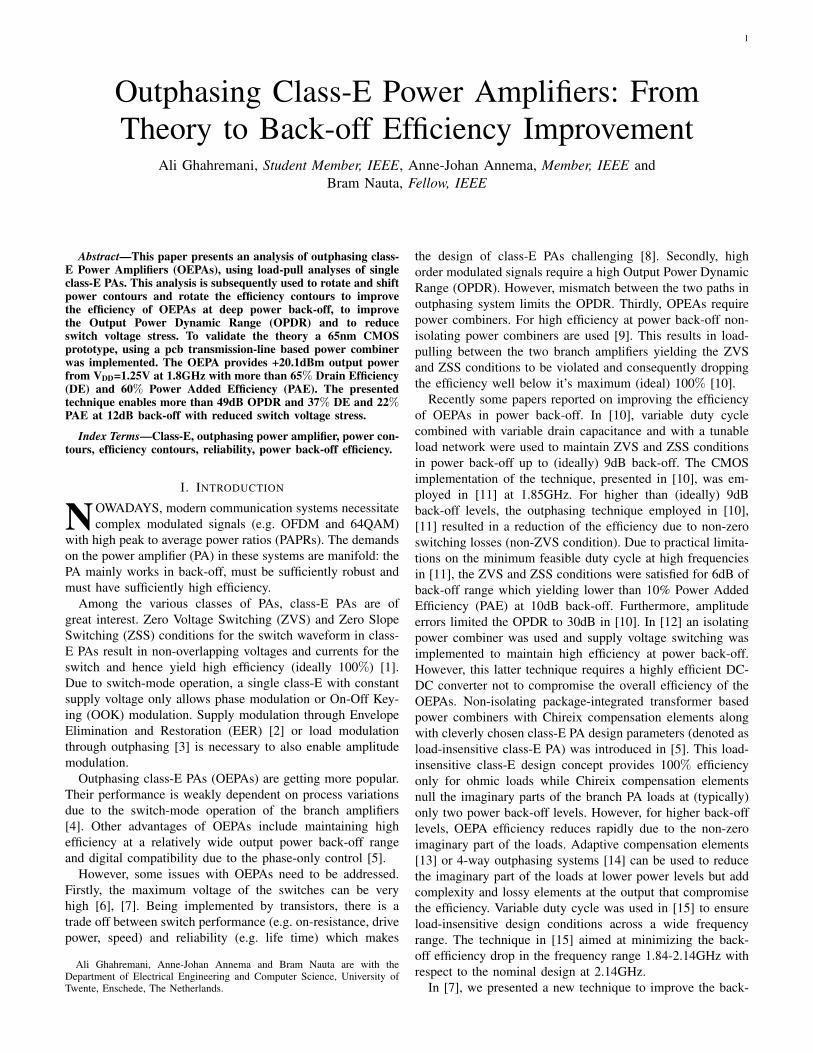
Fig. 1a shows a class-E PA, where the MOS transistoracts as a switch driven by a square wave input signal with(angular) frequency ω0 and duty cycle scaling factor of dwhere d = 1 corresponds to 50% duty cycle. The generalswitching conditions are defined as
vc
(2π
ω0
)= αVDD and
dvcdt
(2π
ω0
)= βω0VDD (1)
where vc and VDD are the switch and supply voltage, respec-tively. L and C form the primary LC-tank to shape the switchvoltage according to the required values of α and β, shownin Fig. 1b, [25], [26]. The relative resonance frequency of thistank is defined [21] as
q =1
ω0
√LC
(2)
The second tank, by L0 and C0, is a band pass filter to filter outload current harmonics. A matching network (not shown herefor simplicity) provides the load of the PA (R+ jX) from thenominal 50Ω antenna impedance. The relation between circuitelements (L, C, X and R), VDD, ω0 and output power Poutare formulated by a K-design set [21]:
K = KL,KC ,KX ,KP = Lω0
R,RCω0,
X
R,RPoutV 2DD
(3)
The K-design set for non-ZVS, non-ZSS, arbitrary d and qand taking into account the switch resistance Ron is derivedin [6], yielding K = K(q, d,m, α, β), where m = ω0RonC.
A. Load-pulling class-E PAs
For the so-called load-insensitive design [5], [27], a class-EPA is conventionally designed to have q = 1.3, d = 1, ZVS(α = 0) and ZSS (β = 0). Assuming an ideal switch, (m =0), the K-design set elements can be obtained from e.g. [6]as KL,KC ,KX ,KP = 1.04, 0.58, 0.28, 1.26. For givenPout, ω0 and VDD, the component values in Fig. 1a can thenbe calculated from the K-design set equations in (3).
For a load-pulling analysis, this ideal class-E PA is subjectedto different loads. For this, jX is kept constant and only the
3
VDD
L
C
L0 C0
@ω0
vC
is
iR
00
1
2
3
4
dπ/ω0
vC(t
)/V
DD
α
θ
tan(θ)=β
ω0
dπ
ω0
2π
time
(b)(a)
RjX
vout
Z
0d
B
-3d
B
-6d
B
100%
80%
60%40%
80%
60%40%
-10d
B
(c)
3
3.6
4
1.1
1
1.1
(d)
2π/ω0
Fig. 1. (a) Single-ended Class-E PA, (b) normalized switch voltage. Load-pullplots for q = 1.3, d = 1 and m = 0, (c) normalized output power (solid)and efficiency (dotted) contours, (d) maximum switch voltage normalized toVDD (solid) and normalized output voltage amplitude (dotted).
load impedance Z, represented by its nominal (real) value Rin Fig. 1a, is changed. For simplicity we normalize both thereal and imaginary part of Z to R:
Z = kR+ jk′R (4)
Note that for the nominal load, k = 1 and k′ = 0. For fixed q,d and m, under non-nominal load conditions ZVS and/or ZSSconditions are violated. A full mathematical derivation of theswitch voltage and current is beyond the scope of this paperand can be found in e.g. [6].
These equations can be rewritten to get important propertiesof both the switch voltage vC(t) and the switch current is(t).This allows to derive e.g. Pout normalized to that at nominalload conditions, the efficiency, the maximum switch voltageVc,Max. normalized to VDD and the output voltage amplitudeVout normalized to that at nominal load conditions. All thesecan be derived as a function of k and k′ as defined in (4),independent from Pout at nominal conditions, the frequencyand the nominal load value R. As a result, for any set of q, dand m, we can now plot contours on a Smith chart with R asthe reference impedance, showing the impact of load changeson the performance and behavior of class-E PAs.
For example for a load-insensitive class-E PA with an idealswitch (m = 0), the load-pull contours are shown in Fig.1c and d for a part of Smith chart. The normalized outputpower and the efficiency contours are shown in Fig. 1c withsolid and dotted lines, respectively. Fig. 1c shows that forreal loads (for impedances ReZ ≥ R) the efficiency is(ideally) 100% while the output power can be lowered. Anon-zero imaginary part of the load will result in α 6= 0 atswitching moment and hence causes switching loss (because ofdischarging the non-zero capacitor voltage) which reduces theefficiency. Vc,Max. contours normalized to VDD are shown inFig. 1d. For real loads (ReZ ≥ R) the Vc,Max. stays close to(but is lower than) that for the nominal load. Toward the upper
0d
B
-3d
B
-6d
B
100%
80%
60%40%
80%60%
40%
-10d
B
(a)
4
(b)
0.930.95
0.95
1
100%
(c)
3
4
(d)
1.05
80%60%40%
80%
40%60%
0d
B
-3d
B
-6d
B-1
0d
B
1.1
5
1.1
1.2
3
Fig. 2. Effect of changing q from 1.3 to 1.2 (a,b), respectively 1.4 (c,d) onthe load-pull plots for d = 1 and m = 0. (a,c) Normalized output power(solid) and efficiency (dotted) contours. (c,d) Vc,Max. normalized to VDD(solid) and normalized output voltage amplitude (dotted).
side of the Smith chart the Vc,Max. increases. Normalizedoutput voltage amplitude across the load, shown in Fig. 1d,shows a symmetrical behavior with respect to real axis. Theseload-pull contours will be used in the next section to describethe behavior of OEPAs and to introduce our method to increasepower efficiency in back-off.
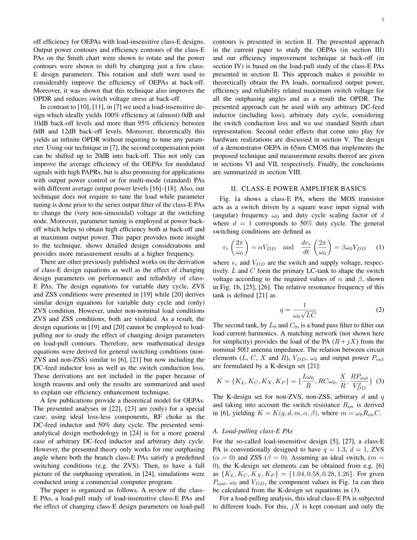
B. Effect of changing q and d on the load-pull contours
Parameters q and d have a major impact on the load-pullcontours shown in Fig. 1. In this section we assume that theclass-E PA is initially designed for q = 1.3 and d = 1. Thenwe change the parameter q (by e.g. changing the capacitor C)and/or change the parameter d and plot the resulting load-pullcontours. Again, these contours are independent from Pout,ω0 and the nominal load R.
The load-pull plots are shown in Fig. 2 for changing q from1.3 to 1.2, respectively 1.4. The shape of the normalized outputpower, efficiency and Vc,Max. contours hardly change exceptfor a rotation: there is clockwise (anti-clockwise) rotation forhigher (lower) q. The normalized output voltage contours,shown in Fig. 2b and d, are rotated and changed in shape.Similar contours can be derived and plotted to show the effectof changing d; then clockwise (anti-clockwise) rotation occursfor lower (higher) d. These plots are shown in Appendix A.
III. SIMPLIFIED THEORY OF OEPAS
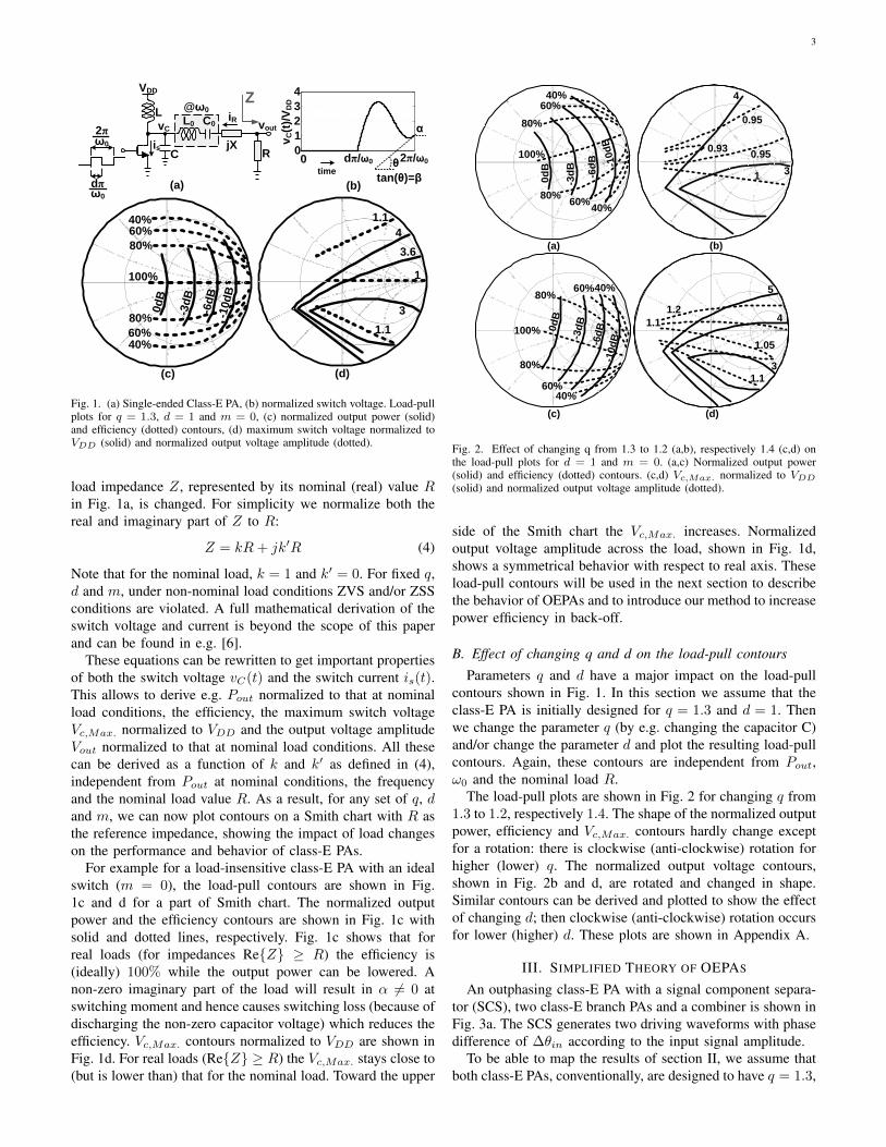
An outphasing class-E PA with a signal component separa-tor (SCS), two class-E branch PAs and a combiner is shown inFig. 3a. The SCS generates two driving waveforms with phasedifference of ∆θin according to the input signal amplitude.
To be able to map the results of section II, we assume thatboth class-E PAs, conventionally, are designed to have q = 1.3,
4
VDD
L
C
L0 C0
jBc
VDD
L
C
L0 C0
-jBc
Δθin SCSvin
Z1
Z2
vout1
vout2
RL=
50
Ω
λ
4
Combiner
Z0
Z0
λ
4
Vout1
Vout2
Vout vout Δθout
jX
vA
jX
vB
-30 -25 -20 -15 -10 -5 00
20
40
60
80
100
Normalized Pout (dB)
Eff
icie
nc
y (
%)
(c)
@10dB
2.5
3
3.5
4
4.5
PA1
PA2
Vc
,Ma
x./V
DD
Z2(Δθout)
Z1(Δθout)Reference
impedance: R
(b)
(a)
Fig. 3. (a) Outphasing class-E PA with transmission-line based combiner.(b) Z1,2 for 0 < ∆θout < π and compensation at outphasing angles π
5and π − π
5. (c) Efficiency vs normalized output power (solid) and Vc,Max.
normalized to VDD for PA1 (dotted-grey) and PA2 (dotted-dark).
d = 1 and α = β = 0 for a load Z1 = Z2 = R. Thecombiner at the output sums the output voltages to reconstructan amplified replica of the input signal. Two compensatingelements, ±jBc are used to compensate the imaginary part ofthe loads at two specific outphasing angles. In this paper atransmission-line based combiner is used.
Let’s consider the part in the dotted box in Fig. 3a andassume voltages at the branch PAs’ outputs as
vout1,2(t) = Vout1,2 sin(ω0t+ φv1,2) (5)
where Vout1,2 and φv1,2 are the amplitudes and initial phaseswith respect to a reference time, respectively. The circuit islinear and can be solved in phasor domain which leads for theapparent load impedances of the two branch PAs to:
1
Z1= +jBc +
RLZ2
0
(1 +
Vout,2Vout,1
e−j∆θout
)1
Z2= −jBc +
RLZ2
0
(1 +
Vout,1Vout,2
e+j∆θout
)(6)
where ∆θout = φv1−φv2 is denoted as the outphasing angle.To simplify the analysis, let’s assume Vout1
Vout2= 1. We will
show the validity of this assumption later in this section. The∆θout-dependent impedance seen by each PA, Z1,2, then is
1
Z1=
2RLZ2
0
cos2(∆θout
2) + j
(−RLZ2
0
sin(∆θout) +Bc
)1
Z2=
2RLZ2
0
cos2(∆θout
2)− j
(−RLZ2
0
sin(∆θout) +Bc
)(7)
where we assume Z0 =√
2RRL. For Bc < RL
Z20
, there are twooutphasing angles for which the imaginary part of the loadsZ1,2 is zero. Z1,2 for a range 0 < ∆θout < π are shown in
Fig. 3b on the Smith chart for Bc = 12Rsin(π/5), assuming
R as the reference impedance.Having PA loads Z1,2, shown in Fig. 3b, on top of the
load-pull contours of the normalized output voltage amplitudeshown in Fig. 1d, yields two important observations. Firstly,the output voltage of the branch PAs is not constant acrossdifferent outphasing angles and therefore, the PAs cannotbe modeled as ideal voltage sources as was done in e.g.[5] (although the same final results for Z1,2 were obtained).Secondly, because of the symmetry of the PA loads Z1,2 andof the normalized output voltages contours with respect to thereal axis, for all outphasing angles Vout,1
Vout,2= 1 which proves
the validity of our assumption leading to (7).To get the output power and the efficiency for an OEPA as
a function of power back-off, the normalized power contoursand the efficiency contours of Fig. 1c can be combined withthe ∆θout-dependent load impedance for the two branch PAsof an OEPA, described in (7) and shown in Fig. 3b. Then foreach ∆θout, the output power and the efficiency of the branchclass-E PAs follow. Due to symmetrical PA loads and contourswith respect to the real axis, the output power and efficiencyof both branch PAs are identical.
Combining the output power as a function of ∆θout and theefficiency as a function of ∆θout yields Fig. 3c, that shows theefficiency of the OEPA plotted versus the (normalized) outputpower. The second compensation point is located at 10dBback-off where the efficiency is (ideally) 100 %. Similarly,the Vc,Max. (normalized to VDD) for the two branch PAs canalso be derived as a function of the power back-off. Fig. 3cshows that the Vc,Max. for PA2 increases at back-off. We willalso address this issue in the measurement section. All plots ofFig. 3c are valid under the assumption of an ideal OEPA withan ideal combiner and assuming a very high loaded qualityfactor for the L0 − C0 filter.
A. Output Vectors’ Amplitude Mismatch
In theory, the branch class-E PAs are identical and hencehave 0% mismatch/error between the output voltage ampli-tudes Vout,1,2. The normalized output power, shown in Fig.3c, is then 0 for ∆θout = π which yields an infinite OPDR.
Any mismatch between the two paths in an outphasingsystem that causes amplitude errors between the two outputvectors Vout1 and Vout2, reduces the OPDR. Using the vectordiagram in Fig. 3a and assuming a relative amplitude error εbetween the two vectors, Vout1 = V and Vout2 = V (1 + ε),the maximum attainable OPDR can then be written as
OPDR(dB) = 20 log
(max(Vout)
min(Vout)
)= 20 log(1 +
2
ε) (8)
Using (8), to have an OPDR better than 60dB [27], theamplitude error should be kept below 0.2 % while mismatchless than 6.5% keeps the OPDR better than 30dB [10].
One of the mechanisms that leads to amplitude error, is theresidual impedance of the series filter L0 − C0 due to e.g.frequency deviations or components spread. For instance, the
5
residual impedance at ∆ω deviation from the center frequencyω0 = 1√
L0C0can be written as
Zr(∆ω) = L0(ω0 + ∆ω)j − j
C0(ω0 + ∆ω)≈ 2L0∆ωj (9)
For ∆ω = 0, Zr = 0 and the filter passes the first harmonicof the signal without any error. However, non-zero Zr causesa voltage division at the inputs of the combiner and hencecreates error.
To find a simple quantitative model, consider the OEPAsystem, shown in Fig. 3a and assume that, for small ∆ω,the combiner, the q parameters, the compensation elementsimpedance and the first harmonic of the signals at nodes Aand B (before the filter) are not affected. Then we can assumeidentical first harmonics VA = VB = V for nodes A and Bfor identical class-E branch PAs. For minimum output power,∆θout = π, and therefore Vout1 and Vout2 can be written as
Vout1(∆θout = π) =Z1VAZ1 + Zr
=V
1− 2L0Bc∆ω
Vout2(∆θout = π) =Z2VBZ2 + Zr
=V
1 + 2L0Bc∆ω(10)
where we replaced Z1 and Z2 from (7) for ∆θout = π and Zrfrom (9). Assuming the loaded Q of the filter as QL = L0ω0
Rand locating the second compensation point at 10dB back-off(Bc = sin(π/5)/2R),
Vout1Vout2
(∆θout = π) =1 +QL sin(π5 )∆ω
ω0
1−QL sin(π5 )∆ωω0
(11)
QL=5, ∆ωω0
=+1% and ∆ωω0
=+5% yield Vout1
Vout2equal to 1.06
and 1.34, respectively. According to (8), and assuming thatZr will not affect maximum Pout, these amplitude errors limitOPDR to 30dB respectively 16dB. Moreover, ∆ω
ω0=-1% and
∆ωω0
=-5% results in Vout1
Vout2equal to 0.94 and 0.74, respectively,
which limits OPDR to 31dB and 19dB, respectively.
IV. BACK-OFF EFFICIENCY IMPROVEMENT TECHNIQUE
This section presents detailed discussions of the techniquepresented in [7] to improve the back-off efficiency of theOEPAs. The starting point is again a conventional OEPA withq1 = q2 = 1.3 and with the second compensation pointslocated at 10dB back-off.
A. Rotation
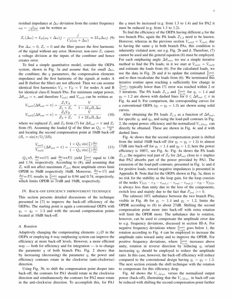
Adaptively changing the compensating elements ±jB in theOEPA or employing 4-way outphasing system can improve theefficiency at more back-off levels. However, a more efficientway — both for efficiency and for integration — is to changethe parameter q of both branch PAs. Fig. 2 shows thatby increasing (decreasing) the parameter q, the power andefficiency contours rotate in the clockwise (anti-clockwise)direction.
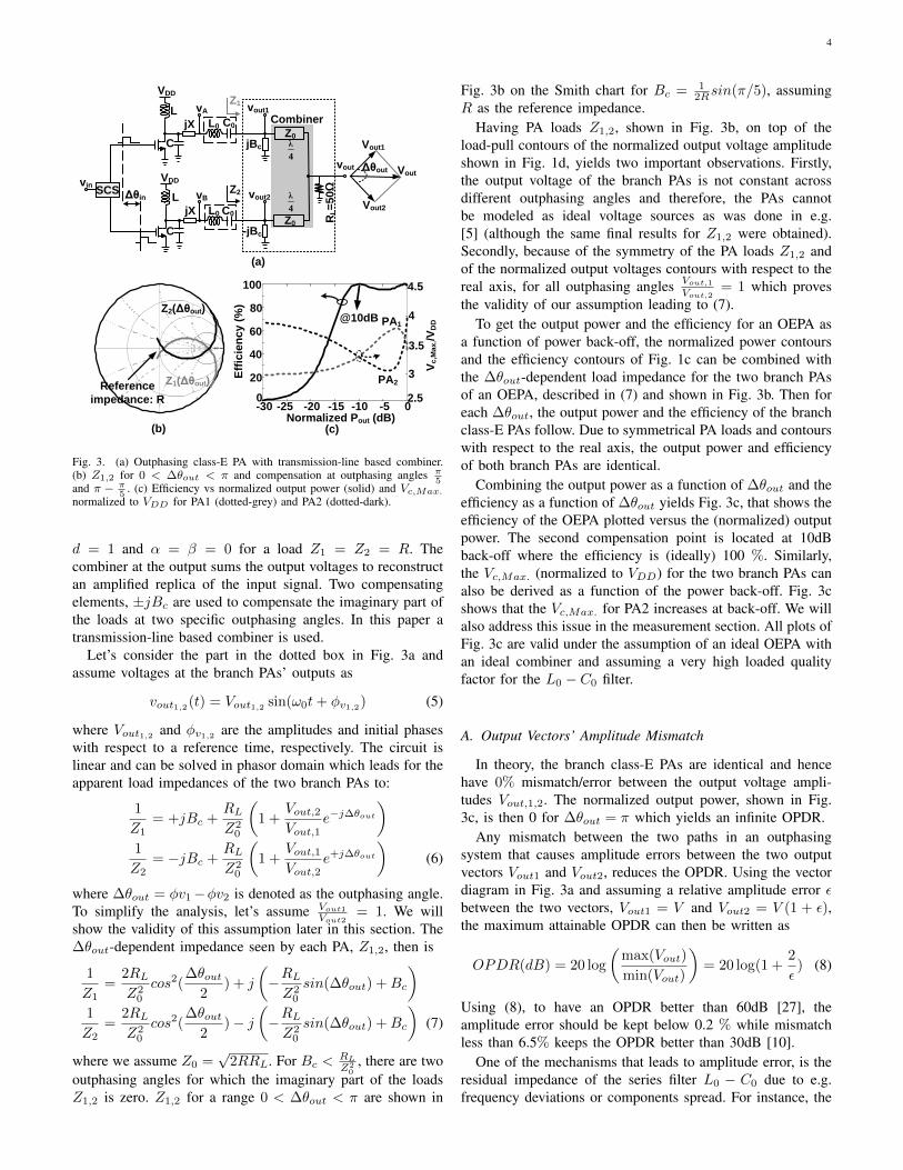
Using Fig. 3b, to shift the compensation point deeper intoback-off, the contours for PA1 should rotate in the clockwisedirection and simultaneously the contours for PA2 must rotatein the anti-clockwise direction. To accomplish this, for PA1
the q must be increased (e.g. from 1.3 to 1.4) and for PA2 itmust be reduced (e.g. from 1.3 to 1.2).
To find the efficiency of the OEPA having different q for thetwo branch PAs, again the PA loads Z1,2 need to be known.However, whereas in the previous section Vout2 = Vout1 dueto having the same q in both branch PAs, this condition isinherently violated now, see e.g. Fig. 2b and d. Therefore, (7)cannot be used and the general equation (6) must be employed.For each outphasing angle ∆θout, we use a simple iterativemethod to find the PA loads; in it we start at Vout1 = Vout2and estimate the loads from (6). For the calculated loads, weuse the data in Fig. 2b and d to update the estimated Vout1
Vout2
and to then recalculate the loads from (6). We terminated thisiterative routine upon reaching a sufficiently low change inVout1
Vout2; typically lower than 1% error was reached within 2 or
3 iterations. The PA loads Z1,2 and Vout1
Vout2for q1 = 1.4 and
q2 = 1.2 are shown with dashed lines for 0 ≤ ∆θout ≤ π inFig. 4a and b. For comparison, the corresponding curves fora conventional OEPA (q1 = q2 = 1.3) are shown using solidcurves.
After obtaining the PA loads Z1,2 as a function of ∆θout,for specific q1 and q2, and using the load-pull contours in Fig.2, the output power, efficiency and the normalized Vc,Max. candirectly be obtained. These are shown in Fig. 4c and d withdashed lines.
Fig. 4c shows that the second compensation point is shiftedfrom the initial 10dB back-off (for q1 = q2 = 1.3) to almost17dB into back-off for q1 = 1.4 and q2 = 1.2; here the powerefficiency is 100%, see Fig. 4c. Fig. 4a shows the PA loadsZ1,2; the negative real part of Z2 for ∆θout close to π impliesthat PA2 absorbs part of the power provided by PA1. Theextension of the load-pull contours, presented in Fig. 1c and dfor positive loads, toward negative impedances is presented inAppendix B. Note that for the OEPA shown in Fig. 3a, there isno risk for the stability as the loop gain, for the loop consistsof the nodes VDD − vA − vout,1 − vout − vout,2 − vB − VDD,is always less than unity due to the loss of the components,switch loss and mainly due to the fact that Pout >= 0.
The (almost) 10% unbalance between the two branch PAs,visible in Fig. 4b for q1 = 1.4 and q2 = 1.2, limits theOPDR according to (8) to about 27dB. Shifting the secondcompensation point more into back-off with extra rotationwill limit the OPDR more. The unbalance due to rotation,however, can be used to compensate the amplitude error dueto e.g. frequency deviations, discussed in section III-A. Fornegative frequency deviations where Vout1
Vout2goes below 1, the
rotation according to Fig. 4 can be employed to increase theamplitude ratio toward unity and to improve the OPDR. Forpositive frequency deviations, where Vout1
Vout2increases above
unity, rotation in reverse direction by reducing q1 or/andincreasing q2 should be employed to reduce the amplituderatio. In this case, however, the back-off efficiency will reducecompared to the conventional design having q1 = q2 = 1.3.The next section extends the shift technique with the rotationto compensate for this efficiency drop.
Fig. 4d shows the Vc,Max. versus the normalized outputpower (back-off), illustrating that the Vc,Max. in back-off canbe reduced with shifting the second compensation point further
6
-30 -25 -20 -15 -10 -5 00
20
40
60
80
100
-30 -25 -20 -15 -10 -5 02
2.5
3
3.5
4.5
Normalized Pout (dB) Normalized Pout (dB)
Eff
icie
nc
y (
%)
Vc,M
ax
./VD
D
(b)
(c) (d)
@10dB
Z1(Δθout)
q1=q2=1.3 (d=1)q1=1.4, q2=1.2 (d=1)
Reference
impedance: R
Δθout(rad)
Vout1
Vout2
Z2(Δθout)
@16.7dB
0 1 2 3 40.9
1
1.1
1.2
1.3
1.4
q1=1.25, q2=1.02 (d=0.7)
@20dB
(a)
4
Fig. 4. Ideal OEPA results for 0 ≤ ∆θout ≤ π for conventional design withq1 = q2 = 1.3 (solid), for rotation with q1 = 1.4 and q2 = 1.2 (dashed)and for shift-rotation with d = 0.7, q1 = 1.25 and q2 = 1.02 (dotted):(a) PA loads Z1 (grey) and Z2 (dark) , (b) Vout1
Vout2vs ∆θout, (c) efficiency
vs normalized output power and (d) Vc,Max. normalized to VDD for PA1(grey) and PA2 (dark).
into back-off.
B. Shift
Reducing the parameters d and q for both branch PAs resultsin rotation in the opposite directions. Therefore, for a lowerd (e.g. 0.7), a lower q (e.g. 1.1) can be found to have almostsame efficiency contours for the branch PAs at a lower outputpower level. This corresponds to a shift of power contours tothe left on Smith chart for almost the same efficiency contours.As a result the output power at (e.g.) the second compensationpoint can be lowered while the efficiency is 100%: the secondcompensation can be shifted to a lower output power levels.
This technique can be combined with the rotation techniqueto shift the second compensation point more into back-off.For this, the d for both branch PAs are reduced to 0.7 forq1 = q2 =1.1 to shift the power contours. Subsequently q1
is increased to 1.25 and q2 is reduced to 1.02 to rotate boththe power and the efficiency contours. Following the sameprocedure as in the previous section, the load-pull contourscan be plotted and a simple iterative procedure can be usedto find Vout1
Vout2for each ∆θout which results in the PA loads
Z1,2. For length reasons the load-pull contours are not shownhere but the effect of the shift-rotation technique on the OEPAperformance and behavior is shown in Fig. 4 with dottedlines. Fig. 4b shows that the output voltage amplitude errorfirst increases with ∆θout, and again reduces when ∆θoutapproaches π, which therefore helps to improve the efficiencywithout sacrificing the OPDR.
Fig. 4c shows that the second compensation point is nowshifted to almost 20dB into back-off with lower switch volt-age stress deep in back-off. However, by fine tuning of theparameters d, q1 and q2, the second compensation point can
be easily shifted to any arbitrary back-off level between 10dBand 20dB. Furthermore, shifting the power contours can lowerthe maximum output power. For maximum output power andto benefit from the high back-off efficiency that the presentedshift-rotation technique brings to the OEPA, one can tune theparameters d and q dynamically according to the requiredinstantaneous output power.
V. SECOND ORDER EFFECTS
A. Switch conduction loss
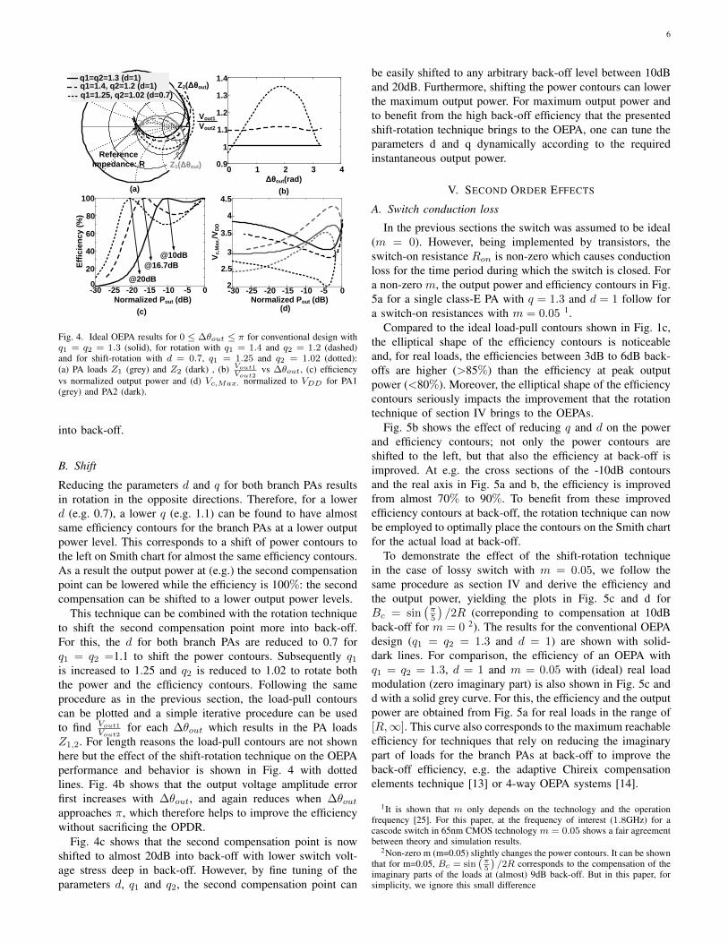
In the previous sections the switch was assumed to be ideal(m = 0). However, being implemented by transistors, theswitch-on resistance Ron is non-zero which causes conductionloss for the time period during which the switch is closed. Fora non-zero m, the output power and efficiency contours in Fig.5a for a single class-E PA with q = 1.3 and d = 1 follow fora switch-on resistances with m = 0.05 1.
Compared to the ideal load-pull contours shown in Fig. 1c,the elliptical shape of the efficiency contours is noticeableand, for real loads, the efficiencies between 3dB to 6dB back-offs are higher (>85%) than the efficiency at peak outputpower (<80%). Moreover, the elliptical shape of the efficiencycontours seriously impacts the improvement that the rotationtechnique of section IV brings to the OEPAs.
Fig. 5b shows the effect of reducing q and d on the powerand efficiency contours; not only the power contours areshifted to the left, but that also the efficiency at back-off isimproved. At e.g. the cross sections of the -10dB contoursand the real axis in Fig. 5a and b, the efficiency is improvedfrom almost 70% to 90%. To benefit from these improvedefficiency contours at back-off, the rotation technique can nowbe employed to optimally place the contours on the Smith chartfor the actual load at back-off.
To demonstrate the effect of the shift-rotation techniquein the case of lossy switch with m = 0.05, we follow thesame procedure as section IV and derive the efficiency andthe output power, yielding the plots in Fig. 5c and d forBc = sin
(π5
)/2R (correponding to compensation at 10dB
back-off for m = 0 2). The results for the conventional OEPAdesign (q1 = q2 = 1.3 and d = 1) are shown with solid-dark lines. For comparison, the efficiency of an OEPA withq1 = q2 = 1.3, d = 1 and m = 0.05 with (ideal) real loadmodulation (zero imaginary part) is also shown in Fig. 5c andd with a solid grey curve. For this, the efficiency and the outputpower are obtained from Fig. 5a for real loads in the range of[R,∞]. This curve also corresponds to the maximum reachableefficiency for techniques that rely on reducing the imaginarypart of loads for the branch PAs at back-off to improve theback-off efficiency, e.g. the adaptive Chireix compensationelements technique [13] or 4-way OEPA systems [14].
1It is shown that m only depends on the technology and the operationfrequency [25]. For this paper, at the frequency of interest (1.8GHz) for acascode switch in 65nm CMOS technology m = 0.05 shows a fair agreementbetween theory and simulation results.
2Non-zero m (m=0.05) slightly changes the power contours. It can be shownthat for m=0.05, Bc = sin
(π5
)/2R corresponds to the compensation of the
imaginary parts of the loads at (almost) 9dB back-off. But in this paper, forsimplicity, we ignore this small difference
7
-30 -25 -20 -15 -10 -5 00
20
40
60
80
100
Normalized Pout (dB)
(c)
Eff
icie
nc
y (
%)
q1=q2=1.3 (d=1)q1=1.4, q2=1.2 (d=1)
OEPA with q1=q2=1.3,
d=1, m=0.05 and
ideal load modulation
-30 -25 -20 -15 -10 -5 00
20
40
60
80
100
Normalized Pout (dB)
(d)
Eff
icie
nc
y (
%)
q1=q2=1.3 (d=1)q1=1.25, q2=1.02 (d=0.7)q1=1.18, q2=0.95 (d=0.5)
0d
B
60%
40%
80%
85%
0dB
-3dB
-6dB
60%
40%
80%
-10dB
90%
60%40%
(a) (b)
-3dB
-6dB
-10dB
Fig. 5. (a,b) The output power (solid) and the efficiency (dotted) contoursfor a single class-E PA with (a) q = 1.3, d = 1 and m = 0.05 and (b) qand d are reduced to 1.1 and 0.7, respectively. (c,d) The efficiency versusnormalized output power for an OEPA with m = 0.05 for the class-E branchPAs and with conventional design and compensation at 10dB back-off (solid-dark), with an ideal load modulation with zero imaginary part (solid-grey),with the rotation (dashed-dark), with the shift-rotation with setting Sett. 1(dotted-dark) and the shift-rotation with setting Sett. 2 (dashed-dotted-dark).
Fig. 5c shows that compensation at 10dB back-off for aconventional OEPA, with q1 = q2 = 1.3, d = 1, having alossy switch can achieve the maximum reachable efficiency(80% for m = 0.05) at full power and near 10dB back-off.The figure also shows that the rotation technique can improvethe efficiency at more than 15dB back-off. Comparing Fig.5c and 4c also clearly shows that the switch conduction lossseriously impact the improvement of our proposed rotationtechnique as well as achieved by the adaptive tuning (or 4-way OEPA). On top of that, also additional losses of thetuning elements or due to extra components at the output cancompromise this improvement. This last issue is also addressedin the measurements section.
Fig. 5d shows the effect of shift-rotation technique onthe efficiency for two different settings Sett.1:q1, q2, d =1.25, 1.02, 0.7 and Sett.2:q1, q2, d = 1.18, 0.95, 0.5with dotted and dashed-dotted curves, respectively. The shift-rotation technique can significantly increase the efficiencyin back-off: e.g. the efficiency is improved from less than10% to more than 75% at 20dB back-off (more than ×7.5improvement).
B. Limited quality factor of the DC-feed inductor L
Another important loss mechanism is due to the limitedquality factor (Q) of the DC-feed inductor L, shown in Fig.3a. This inductor can be a separate component [7] or it can bea part of the transformer-based combiner [5], [27]. To studythis effect, one can derive a new set of load-pull equationsusing Q as a parameter. This derivation is not given here forsimplicity and length reasons.
-30 -25 -20 -15 -10 -5 00
20
40
60
80
100
Normalized Pout (dB)(b)
Eff
icie
nc
y (
%)
-30 -25 -20 -15 -10 -5 00
20
40
60
80
100
Normalized Pout (dB)
(a)
Eff
icie
nc
y (
%)
Q=30, m=0.05 Q=30, m=0.1
OEPA with q1=q2=1.3, d=1
and ideal load modulation
q1=q2=1.3 (d=1)q1=1.4, q2=1.2 (d=1)q1=1.18, q2=0.95 (d=0.5)
@-20dB: 5→23 (×4.6) @-15dB: 19→42 (×2.2)
@-20dB: 3→16 (×5.3) @-15dB: 11→36 (×3.3)
Fig. 6. The efficiency versus normalized output power for a conventionalOEPA with q1 = q2 = 1.3 and compensation at 10dB back-off (solid-dark)and with an ideal load modulation (solid-grey), the rotation (dashed-dark),the shift-rotation with setting Sett. 2 (dotted-dark): (a) m = 0.05 and (b)m = 0.1.
The resulting efficiency versus power curves for m = 0.05and m = 0.1 and for quality factor value Q = 30 are shownin Fig. 6 for the conventional OEPA design (solid curve) withcompensation at 10dB back-off, using the rotation technique(dashed curve) and for the shift-rotation with setting Sett.2(dotted curve). For comparison, both graphs in Fig. 6 includea solid-grey curve that corresponds to the maximum efficiencyof an OEPA with conventional design and ideal real loadmodulation, for the specific Q and m listed for each graph.Again, these curves represent the upper efficiency limit for anytechnique that optimizes efficiency by reducing the imaginarypart of loads for the branch PAs at back-off [13], [14].
For the both cases, employing only the rotation techniquecan improve the efficiency to the maximum reachable effi-ciency (grey curve) at back-offs up to around 20dB. However,the improvement with respect to a conventional OEPA (blacksolid curve) almost vanishes for high m or low Q. This is dueto compression of the elliptical efficiency contours. However,the rotation technique can be used both to reduce the switchvoltage stress at back-off and to improve the OPDR.
The proposed shift-rotation technique, however, improvesthe efficiency at back-off to levels significantly higher thanthe maximum reachable efficiency with real load modulation.Also, the improvement ratio increases with increasing switchconduction loss for a constant Q (the absolute efficiencies arelower though). For instance, at 20dB back-off, more than ×4.6and ×5.3 higher efficiencies with respect to the conventionaldesign are obtained for respectively, m = 0.05 and 0.1. Itcan be concluded that this shift-rotation technique is quitepromising to improve the efficiency of an OEPA with anintegrated combiner at high frequencies e.g. [27], where theswitch conduction is the dominant loss mechanism.
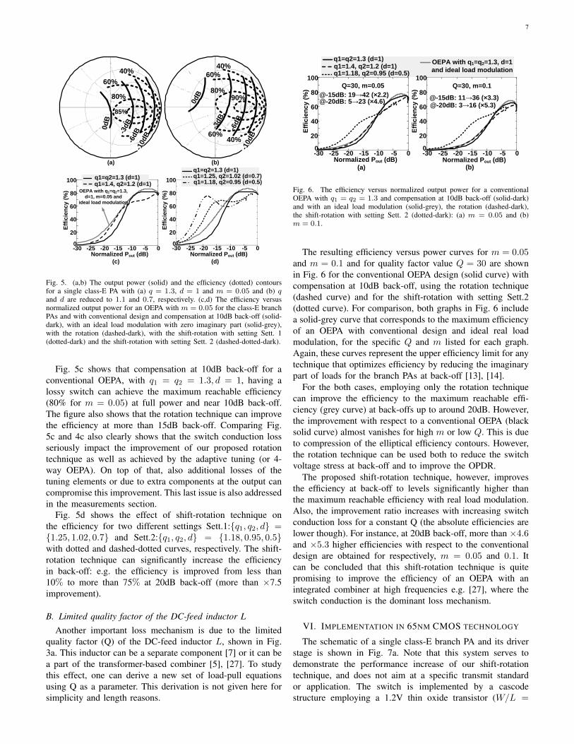
VI. IMPLEMENTATION IN 65NM CMOS TECHNOLOGY
The schematic of a single class-E branch PA and its driverstage is shown in Fig. 7a. Note that this system serves todemonstrate the performance increase of our shift-rotationtechnique, and does not aim at a specific transmit standardor application. The switch is implemented by a cascodestructure employing a 1.2V thin oxide transistor (W/L =
8
0.84mm/60nm) as switch transistor and a thick oxide 2.5Vtransistor (W/L = 1.65mm/280nm) as cascode device. Thecascode structure allows Vc,Max. up to 4V for reliabilityreasons.
Using the K-design set elements for q = 1.3, d = 1,m ≈ 0.05 and α = β = 0 and for R = 15Ω, ω0 = 2π1.8GHz,yields L = 1.4nH, C = 3.3pF and X = 0.5nH. TheDC-feed inductor L is implemented by two parallel bond-wire inductances to provide a relatively high quality factorQ (≈ 25). The tank capacitor C at the switching nodewas implemented with the drain-bulk and gate-drain parasiticcapacitance of the cascode transistor. Moreover, the drain andthe source of the cascode transistor were layed out close toeach other to introduce some parasitic capacitance CP,DS toachieve slightly better efficiency [28]. Two cascaded inverterswere used as the driver for the switch where the duty cyclecan be controlled by the off-chip control voltage Vb.
Two switched capacitor banks with 4 control bits X1 andX2 were used at the switching nodes to tune the q parameterof the branch PAs independently. Circuit simulations in 65nmCMOS technology suggest that a total switchable capacitanceof 1.5pF is more than sufficient to employ the shift-rotationtechnique with shifting the contours up to 5dB. This 1.5pFcapacitor is divided into 4 sections with C1 = 150fF, C2 =300fF, C3 = 450fF and C4 = 600fF, shown in Fig. 7a, beingcontrolled with 4 control switches Si, i ∈ 0, 1, 2, 3.
When each switch Si is off, it needs to tolerate the maxi-mum voltage at the switching node which can be up to 4V. Theswitches Si are implemented by 2.5V thick oxide transistors.There is a parasitic capacitance Cp,Si
associated with theswitch Si, shown in Fig. 7a. The switches Si are sized to haveCp,Si ≈ 1
4Ci to make sure the maximum voltage across theswitches Si does not exceed (almost) 3V. This switch-capacitornetwork at the switching node introduces extra capacitiveloading at this node when all control bits are zero, whichamounts to 0.3pF or 10% of the total drain capacitance. Tocompensate for this extra capacitance, the switch size wasreduced by 10%. This increases m by 10% which impactsthe (simulated) efficiency at maximum output power and atthe back-off by less than 3%.
To have the high and low level of the voltages at the driveroutput well defined, the driver and the main switch sharethe same ground and to reduce the bond-wire inductance atground 6 parallel down-bonds (DBs) with minimum lengthwere used (shown in Fig. 7b). The switches Si are controlledquasi-statically, driven from off-chip sources; no dynamictuning is provided for this paper. The microphotograph of theimplemented branch class-E PA is shown in Fig. 7b.
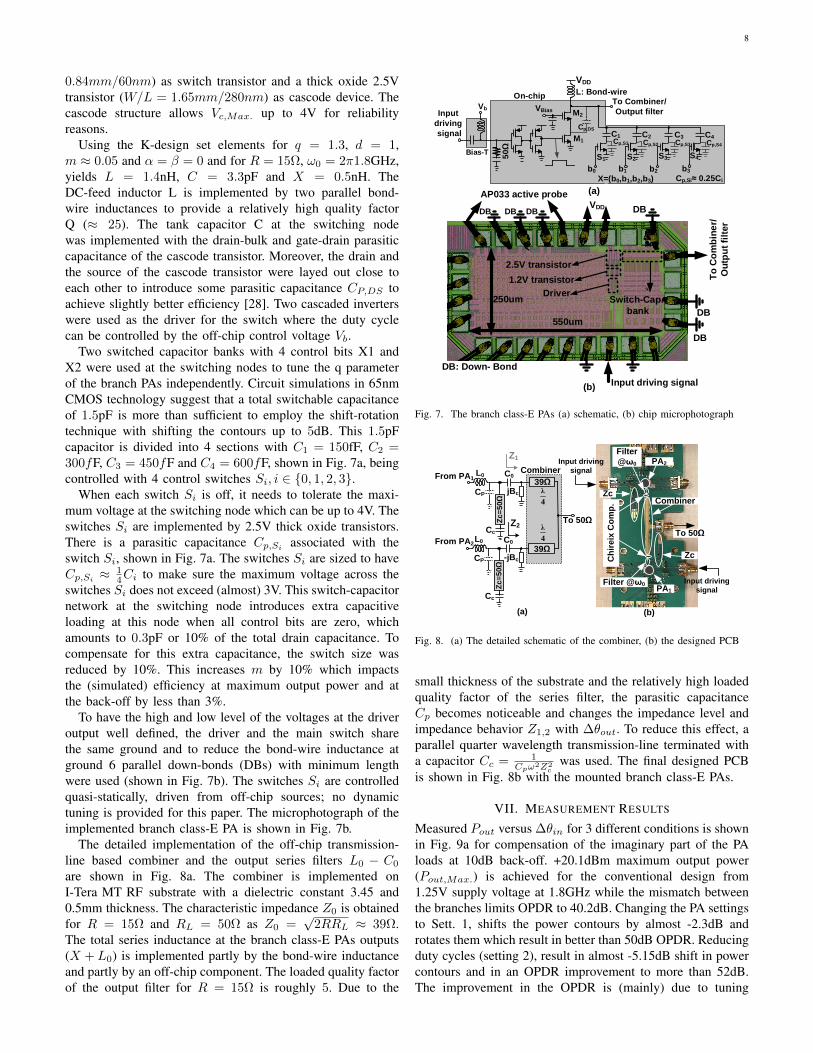
The detailed implementation of the off-chip transmission-line based combiner and the output series filters L0 − C0
are shown in Fig. 8a. The combiner is implemented onI-Tera MT RF substrate with a dielectric constant 3.45 and0.5mm thickness. The characteristic impedance Z0 is obtainedfor R = 15Ω and RL = 50Ω as Z0 =
√2RRL ≈ 39Ω.
The total series inductance at the branch class-E PAs outputs(X + L0) is implemented partly by the bond-wire inductanceand partly by an off-chip component. The loaded quality factorof the output filter for R = 15Ω is roughly 5. Due to the
VDD
L: Bond-wire
M1
M2VBias
Vb
On-chip
Bias-T
50
b0 b1 b2 b3
X=(b0,b1,b2,b3)
C1
(a)
C2 C3 C4
Cp,DS
S1 S2 S3 S4
Cp,S1 Cp,S2 Cp,S3 Cp,S4
Cp,Si 0.25Ci
(b)
To Combiner/
Output filter
VDD
AP033 active probe
2.5V transistor
1.2V transistor
Driver
550um
250um
Input driving signal
Switch-Cap.
bank
To
Co
mb
ine
r/
Ou
tpu
t fi
lter
DB
DBDB DB DB
Input
driving
signal
DB
DB: Down- Bond
Fig. 7. The branch class-E PAs (a) schematic, (b) chip microphotograph
PA1
Filter @ω0
Ch
ire
ix C
om
p. Combiner
(b)
L0 C0
jBc
-jBc
Z1
To 50Ω
λ
4
Combiner
39Ω
λ
4
(a)
39Ω
CPZ
c=
50Ω
Cc
L0 C0
Z2
CP
Zc
=5
0Ω
Cc
Zc
Zc
From PA1
From PA2
PA2
Filter
@ω0
Input driving
signal
Input driving
signal
To 50Ω
Fig. 8. (a) The detailed schematic of the combiner, (b) the designed PCB
small thickness of the substrate and the relatively high loadedquality factor of the series filter, the parasitic capacitanceCp becomes noticeable and changes the impedance level andimpedance behavior Z1,2 with ∆θout. To reduce this effect, aparallel quarter wavelength transmission-line terminated witha capacitor Cc = 1
Cpω2Z2c
was used. The final designed PCBis shown in Fig. 8b with the mounted branch class-E PAs.
VII. MEASUREMENT RESULTS
Measured Pout versus ∆θin for 3 different conditions is shownin Fig. 9a for compensation of the imaginary part of the PAloads at 10dB back-off. +20.1dBm maximum output power(Pout,Max.) is achieved for the conventional design from1.25V supply voltage at 1.8GHz while the mismatch betweenthe branches limits OPDR to 40.2dB. Changing the PA settingsto Sett. 1, shifts the power contours by almost -2.3dB androtates them which result in better than 50dB OPDR. Reducingduty cycles (setting 2), result in almost -5.15dB shift in powercontours and in an OPDR improvement to more than 52dB.The improvement in the OPDR is (mainly) due to tuning
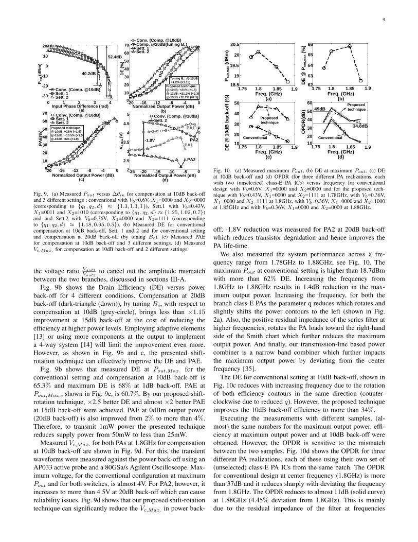
9
-20 -16 -12 -8 -4 00
10
20
30
40
50
60
70Sett. 1
Normalized Output Power (dB)
DE
(%
)
Tuning Bc: @-15dB:
+1.2% (×1.15)
Proposed technique:
@-10dB: +21% (×1.8)
@-12dB: +21.2% (×2.3)
@-15dB:+12.7% (×2.5)
Sett. 2
-20 -16 -12 -8 -4 00
10
20
30
40
50
60
70
Normalized Output Power (dB)
PA
E(%
)P
ou
t (d
Bm
)
0 1 2 3 4
-30
-20
-10
0
10
20
Input Phase Difference (rad)
40.2dB
52.4dB
Sett. 1
(a) (b)
(c)
Sett. 2
Comp. @20dB(tuning Bc)
Conv. (Comp. @10dB)
Proposed technique:
@-10dB: +11% (×1.6)
@-12dB: +10.5% (×1.9)
@-15dB:+6% (×1.9)
-25 -20 -15 -10 -5 02
2.5
3.5
4
4.5
5
PA1
PA1
PA2
PA2
-1.8V
Normalized Output Power (dB)(d)
Vc
,Ma
x.(V
)Sett. 1Sett. 2
Sett. 2
3
Conv. (Comp. @10dB) Conv. (Comp. @10dB)
Conv. (Comp. @10dB)
Fig. 9. (a) Measured Pout versus ∆θin for compensation at 10dB back-offand 3 different settings ; conventional with Vb=0.6V, X1=0000 and X2=0000(corresponding to q1, q2, d ≈ 1.3, 1.3, 1), Sett.1 with Vb=0.43V,X1=0011 and X2=1010 (corresponding to q1, q2, d ≈ 1.25, 1.02, 0.7)and and Sett.2 with Vb=0.36V, X1=0000 and X2=1111 (correspondingto q1, q2, d ≈ 1.18, 0.95, 0.5). (b) Measured DE for conventionalcompensation at 10dB back-off, Sett. 1 and 2 and for conventional settingand compensation at 20dB back-off (by tuning Bc). (c) Measured PAEfor compensation at 10dB back-off and 3 different settings. (d) MeasuredVc,Max. for compensation at 10dB back-off and 2 different settings.
the voltage ratio Vout1
Vout2to cancel out the amplitude mismatch
between the two branches, discussed in sections III-A.Fig. 9b shows the Drain Efficiency (DE) versus power
back-off for 4 different conditions. Compensation at 20dBback-off (dark-triangle (down)), by tuning Bc, with respect tocompensation at 10dB (grey-circle), brings less than ×1.15improvement at 15dB back-off at the cost of reducing theefficiency at higher power levels. Employing adaptive elements[13] or using more components at the output to implementa 4-way system [14] will limit the improvement even more.However, as shown in Fig. 9b and c, the presented shift-rotation technique can effectively improve the DE and PAE.
Fig. 9b shows that measured DE at Pout,Max. for theconventional setting and compensation at 10dB back-off is65.3% and maximum DE is 68% at 1dB back-off. PAE atPout,Max., shown in Fig. 9c, is 60.7%. By our proposed shift-rotation technique, ×2.5 better DE and almost ×2 better PAEat 15dB back-off were achieved. PAE at 0dBm output power(20dB back-off) is also improved from 2% to more than 4%.Therefore, to transmit 1mW power the presented techniquereduces supply power from 50mW to less than 25mW.
Measured Vc,Max. for both PAs at 1.8GHz for compensationat 10dB back-off are shown in Fig. 9d. For this, the transientwaveforms were measured against the power back-off using anAP033 active probe and a 80GSa/s Agilent Oscilloscope. Max-imum voltage, for the conventional configuration at maximumPout and for both switches, is almost 4V. For PA2, however, itincreases to more than 4.5V at 20dB back-off which can causereliability issues. Fig. 9d shows that our proposed shift-rotationtechnique can significantly reduce the Vc,Max. in power back-
1.75 1.8 1.85 1.918.5
19
19.5
20
20.5
1.75 1.8 1.85 1.962
63
64
65
66
10
20
30
40
50
10
20
30
40
50
60
1.75 1.8 1.85 1.9 1.75 1.8 1.85 1.9
DE
@ P
ou
t,m
ax (
%)
OP
DR
(dB
)
DE
@ 1
0d
B b
ac
k-o
ff (
%)
Po
ut,
ma
x (
dB
m)
Freq. (GHz) Freq. (GHz)
Freq. (GHz) Freq. (GHz)
Conventional
Proposed
technique
(a) (b)
(c) (d)
34.8dB
Proposed
technique
Conventional
49dB
Fig. 10. (a) Measured maximum Pout, (b) DE at maximum Pout, (c) DEat 10dB back-off and (d) OPDR (for three different PA realizations, eachwith two (unselected) class-E PA ICs) versus frequency for conventionaldesign with Vb=0.6V, X1=0000 and X2=0000 and for the proposed tech-nique with Vb=0.43V, X1=0000 and X2=1111 at 1.78GHz, with Vb=0.36V,X1=0000 and X2=1111 at 1.8GHz, with Vb=0.36V, X1=0000 and X2=1000at 1.85GHz and with Vb=0.36V, X1=0000 and X2=0000 at 1.88GHz.
off; -1.8V reduction was measured for PA2 at 20dB back-offwhich reduces transistor degradation and hence improves thePA life-time.
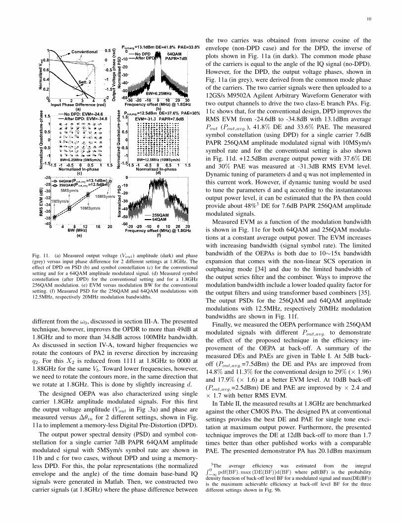
We also measured the system performance across a fre-quency range from 1.78GHz to 1.88GHz, see Fig. 10. Themaximum Pout at conventional setting is higher than 18.7dBmwith more than 62% DE. Increasing the frequency from1.8GHz to 1.88GHz results in 1.4dB reduction in the max-imum output power. Increasing the frequency, for both thebranch class-E PAs the parameter q reduces which rotates andslightly shifts the power contours to the left (shown in Fig.2a). Also, the positive residual impedance of the series filter athigher frequencies, rotates the PA loads toward the right-handside of the Smith chart which further reduces the maximumoutput power. And finally, our transmission-line based powercombiner is a narrow band combiner which further impactsthe maximum output power by deviating from the centerfrequency [35].
The DE for conventional setting at 10dB back-off, shown inFig. 10c reduces with increasing frequency due to the rotationof both efficiency contours in the same direction (counter-clockwise due to reduced q). However, the proposed techniqueimproves the 10dB back-off efficiency to more than 34%.
Executing the measurements with different samples, (al-most) the same numbers for the maximum output power, effi-ciency at maximum output power and at 10dB back-off wereobtained. However, the OPDR is sensitive to the mismatchbetween the two samples. Fig. 10d shows the OPDR for threedifferent PA realizations, each of these using their own set of(unselected) class-E PA ICs from the same batch. The OPDRfor conventional design at center frequency (1.8GHz) is morethan 37dB and it reduces sharply with deviating the frequencyfrom 1.8GHz. The OPDR reduces to almost 11dB (solid curve)at 1.88GHz (4.45% deviation from 1.8GHz). This is mainlydue to the residual impedance of the filter at frequencies
10
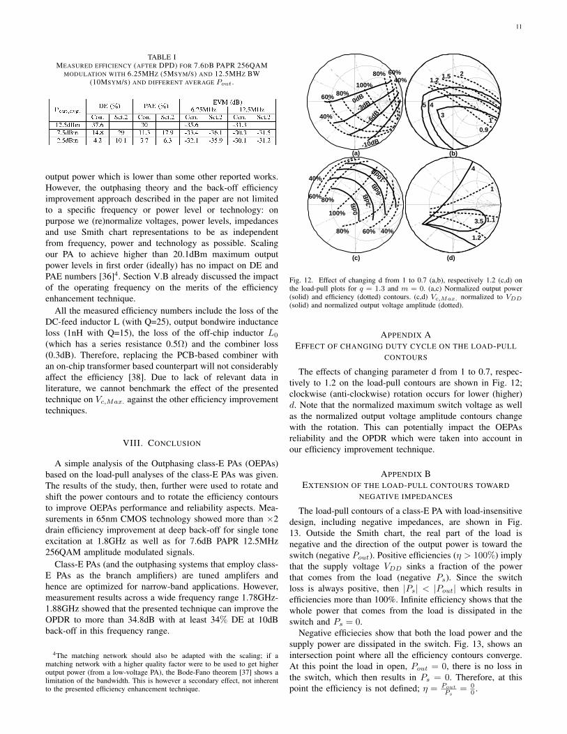
Fig. 11. (a) Measured output voltage (Vout) amplitude (dark) and phase(grey) versus input phase difference for 2 different settings at 1.8GHz. Theeffect of DPD on PSD (b) and symbol constellation (c) for the conventionalsetting and for a 64QAM amplitude modulated signal. (d) Measured symbolconstellation (after DPD) for the conventional setting and for a 1.8GHz256QAM modulation. (e) EVM versus modulation BW for the conventionalsetting. (f) Measured PSD for the 256QAM and 64QAM modulations with12.5MHz, respectively 20MHz modulation bandwidths.
different from the ω0, discussed in section III-A. The presentedtechnique, however, improves the OPDR to more than 49dB at1.8GHz and to more than 34.8dB across 100MHz bandwidth.As discussed in section IV-A, toward higher frequencies werotate the contours of PA2 in reverse direction by increasingq2. For this X2 is reduced from 1111 at 1.8GHz to 0000 at1.88GHz for the same Vb. Toward lower frequencies, however,we need to rotate the contours more, in the same direction thatwe rotate at 1.8GHz. This is done by slightly increasing d.
The designed OEPA was also characterized using singlecarrier 1.8GHz amplitude modulated signals. For this firstthe output voltage amplitude (Vout in Fig .3a) and phase aremeasured versus ∆θin for 2 different settings, shown in Fig.11a to implement a memory-less Digital Pre-Distortion (DPD).
The output power spectral density (PSD) and symbol con-stellation for a single carrier 7dB PAPR 64QAM amplitudemodulated signal with 5MSym/s symbol rate are shown in11b and c for two cases, without DPD and using a memory-less DPD. For this, the polar representations (the normalizedenvelope and the angle) of the time domain base-band IQsignals were generated in Matlab. Then, we constructed twocarrier signals (at 1.8GHz) where the phase difference between
the two carries was obtained from inverse cosine of theenvelope (non-DPD case) and for the DPD, the inverse ofplots shown in Fig. 11a (in dark). The common mode phaseof the carriers is equal to the angle of the IQ signal (no-DPD).However, for the DPD, the output voltage phases, shown inFig. 11a (in grey), were derived from the common mode phaseof the carriers. The two carrier signals were then uploaded to a12GS/s M9502A Agilent Arbitrary Waveform Generator withtwo output channels to drive the two class-E branch PAs. Fig.11c shows that, for the conventional design, DPD improves theRMS EVM from -24.6dB to -34.8dB with 13.1dBm averagePout (Pout,avg.), 41.8% DE and 33.6% PAE. The measuredsymbol constellation (using DPD) for a single carrier 7.6dBPAPR 256QAM amplitude modulated signal with 10MSym/ssymbol rate and for the conventional setting is also shownin Fig. 11d. +12.5dBm average output power with 37.6% DEand 30% PAE was measured at -31.3dB RMS EVM level.Dynamic tuning of parameters d and q was not implemented inthis current work. However, if dynamic tuning would be usedto tune the parameters d and q according to the instantaneousoutput power level, it can be estimated that the PA then couldprovide about 48%3 DE for 7.6dB PAPR 256QAM amplitudemodulated signals.
Measured EVM as a function of the modulation bandwidthis shown in Fig. 11e for both 64QAM and 256QAM modula-tions at a constant average output power. The EVM increaseswith increasing bandwidth (signal symbol rate). The limitedbandwidth of the OEPAs is both due to 10∼15x bandwidthexpansion that comes with the non-linear SCS operation inoutphasing mode [34] and due to the limited bandwidth ofthe output series filter and the combiner. Ways to improve themodulation bandwidth include a lower loaded quality factor forthe output filters and using transformer based combiners [35].The output PSDs for the 256QAM and 64QAM amplitudemodulations with 12.5MHz, respectively 20MHz modulationbandwidths are shown in Fig. 11f.
Finally, we measured the OEPA performance with 256QAMmodulated signals with different Pout,avg. to demonstratethe effect of the proposed technique in the efficiency im-provement of the OEPA at back-off. A summary of themeasured DEs and PAEs are given in Table I. At 5dB back-off (Pout,avg.=7.5dBm) the DE and PAs are improved from14.8% and 11.3% for the conventional design to 29% (× 1.96)and 17.9% (× 1.6) at a better EVM level. At 10dB back-off(Pout,avg.=2.5dBm) DE and PAE are improved by × 2.4 and× 1.7 with better RMS EVM.
In Table II, the measured results at 1.8GHz are benchmarkedagainst the other CMOS PAs. The designed PA at conventionalsettings provides the best DE and PAE for single tone exci-tation at maximum output power. Furthermore, the presentedtechnique improves the DE at 12dB back-off to more than 1.7times better than other published works with a comparablePAE. The presented demonstrator PA has 20.1dBm maximum
3The average efficiency was estimated from the integral∫ 0−∞ pdf(BF).max (DE(BF))d(BF) where pdf(BF) is the probability
density function of back-off level BF for a modulated signal and max(DE(BF))is the maximum achievable efficiency at back-off level BF for the threedifferent settings shown in Fig. 9b.
11
TABLE IMEASURED EFFICIENCY (AFTER DPD) FOR 7.6DB PAPR 256QAM
MODULATION WITH 6.25MHZ (5MSYM/S) AND 12.5MHZ BW(10MSYM/S) AND DIFFERENT AVERAGE Pout .
output power which is lower than some other reported works.However, the outphasing theory and the back-off efficiencyimprovement approach described in the paper are not limitedto a specific frequency or power level or technology: onpurpose we (re)normalize voltages, power levels, impedancesand use Smith chart representations to be as independentfrom frequency, power and technology as possible. Scalingour PA to achieve higher than 20.1dBm maximum outputpower levels in first order (ideally) has no impact on DE andPAE numbers [36]4. Section V.B already discussed the impactof the operating frequency on the merits of the efficiencyenhancement technique.
All the measured efficiency numbers include the loss of theDC-feed inductor L (with Q=25), output bondwire inductanceloss (1nH with Q=15), the loss of the off-chip inductor L0
(which has a series resistance 0.5Ω) and the combiner loss(0.3dB). Therefore, replacing the PCB-based combiner withan on-chip transformer based counterpart will not considerablyaffect the efficiency [38]. Due to lack of relevant data inliterature, we cannot benchmark the effect of the presentedtechnique on Vc,Max. against the other efficiency improvementtechniques.
VIII. CONCLUSION
A simple analysis of the Outphasing class-E PAs (OEPAs)based on the load-pull analyses of the class-E PAs was given.The results of the study, then, further were used to rotate andshift the power contours and to rotate the efficiency contoursto improve OEPAs performance and reliability aspects. Mea-surements in 65nm CMOS technology showed more than ×2drain efficiency improvement at deep back-off for single toneexcitation at 1.8GHz as well as for 7.6dB PAPR 12.5MHz256QAM amplitude modulated signals.
Class-E PAs (and the outphasing systems that employ class-E PAs as the branch amplifiers) are tuned amplifers andhence are optimized for narrow-band applications. However,measurement results across a wide frequency range 1.78GHz-1.88GHz showed that the presented technique can improve theOPDR to more than 34.8dB with at least 34% DE at 10dBback-off in this frequency range.
4The matching network should also be adapted with the scaling; if amatching network with a higher quality factor were to be used to get higheroutput power (from a low-voltage PA), the Bode-Fano theorem [37] shows alimitation of the bandwidth. This is however a secondary effect, not inherentto the presented efficiency enhancement technique.
0d
B -3d
B -6dB
100%
80%60%
40%
80% 60% 40%
-10d
B
(a) (b)
100%
(c)
3
4
(d)
0.9
80% 60%
40%
80%
40%
60%0dB
-3dB
-6dB
-10dB
1
5
1.21.5
1.2
1.1
1
2
3.5
4
Fig. 12. Effect of changing d from 1 to 0.7 (a,b), respectively 1.2 (c,d) onthe load-pull plots for q = 1.3 and m = 0. (a,c) Normalized output power(solid) and efficiency (dotted) contours. (c,d) Vc,Max. normalized to VDD(solid) and normalized output voltage amplitude (dotted).
APPENDIX AEFFECT OF CHANGING DUTY CYCLE ON THE LOAD-PULL
CONTOURS
The effects of changing parameter d from 1 to 0.7, respec-tively to 1.2 on the load-pull contours are shown in Fig. 12;clockwise (anti-clockwise) rotation occurs for lower (higher)d. Note that the normalized maximum switch voltage as wellas the normalized output voltage amplitude contours changewith the rotation. This can potentially impact the OEPAsreliability and the OPDR which were taken into account inour efficiency improvement technique.
APPENDIX BEXTENSION OF THE LOAD-PULL CONTOURS TOWARD
NEGATIVE IMPEDANCES
The load-pull contours of a class-E PA with load-insensitivedesign, including negative impedances, are shown in Fig.13. Outside the Smith chart, the real part of the load isnegative and the direction of the output power is toward theswitch (negative Pout). Positive efficiencies (η > 100%) implythat the supply voltage VDD sinks a fraction of the powerthat comes from the load (negative Ps). Since the switchloss is always positive, then |Ps| < |Pout| which results inefficiencies more than 100%. Infinite efficiency shows that thewhole power that comes from the load is dissipated in theswitch and Ps = 0.
Negative efficiecies show that both the load power and thesupply power are dissipated in the switch. Fig. 13, shows anintersection point where all the efficiency contours converge.At this point the load in open, Pout = 0, there is no loss inthe switch, which then results in Ps = 0. Therefore, at thispoint the efficiency is not defined; η = Pout
Ps= 0
0 .
12
TABLE IIPERFORMANCE COMPARISON
100%
80%
60%
40%
80%
60%
40%
(b)
3
3.6
4
1.1
1
1.1
(a)
100%
200%
200%1000%
1000%
-1000%
-1000%
-200%
-100%
-100%
-200%
150%
150%
Fig. 13. Load-pull contours of a class-E PA with load-insensitive designand m = 0. (a) Maximum switch voltage normalized to VDD (solid) andnormalized output voltage amplitude (dotted), (b) normalized output power(solid) and efficiency (dotted) contours.
REFERENCES
[1] F.H. Raab, ”Idealized operation of the class-E tuned power amplifier,” inCircuits and Systems, IEEE Transactions on, vol. 24, no. 12, pp. 725-735,Dec. 1977.
[2] S. C. Cripps, ”RF Power Amplifiers for Wireless Communications,”Norwood, MA: Artech House, pp. 113-143, 219-249.
[3] R. Beltran, F. H. Raab and A. Velazquez, ”HF outphasing transmitterusing class-E power amplifiers,” in IEEE MTT-S International MicrowaveSymposium Digest, 2009, pp. 757-760.
[4] N. O. Sokal and A. D. Sokal, ”Class E-A new class of high-efficiencytuned single-ended switching power amplifiers,” in IEEE Journal of Solid-State Circuits, vol. 10, no. 3, pp. 168-176, June 1975.
[5] M. P. van der Heijden, M. Acar, J. S. Vromans and D. A. Calvillo-Cortes,”A 19W high-efficiency wide-band CMOS-GaN class-E Chireix RFoutphasing power amplifier,” 2011 IEEE MTT-S International MicrowaveSymposium, Baltimore, MD, 2011, pp. 1-4.
[6] R. Sadeghpour, A. Nabavi, ”Design Procedure of Quasi-Class-E PowerAmplifier for Low-Breakdown-Voltage Devices,” Circuits and Systems I:Regular Papers, IEEE Transactions on, vol. 61, no. 5, pp. 1416-1428,May 2014.
[7] A. Ghahremani, A. J. Annema and B. Nauta, ”A 20dBm outphasing classE PA with high efficiency at power back-off in 65nm CMOS technology,”
in IEEE Radio Frequency Integrated Circuits Symposium (RFIC), 2017,pp. 340-343.
[8] I. Aoki, S. Kee, R. Magoon, R. Aparicio, F. Bohn, J. Zachan, G.Hatcher, D. McClymont and A. Hajimiri, ”A Fully-Integrated Quad-BandGSM/GPRS CMOS Power Amplifier,” Solid-State Circuits, IEEE Journalof, vol. 43, no. 12, pp. 2747-2758, Dec. 2008.
[9] M. Ozen, M. van der Heijden, M. Acar, R. Jos and C. Fager, ”AGeneralized Combiner Synthesis Technique for Class-E OutphasingTransmitters,” in IEEE Transactions on Circuits and Systems I: RegularPapers, vol. 64, no. 5, pp. 1126-1139, May 2017.
[10] N. Singhal, H. Zhang and S. Pamarti, ”A Zero-Voltage-SwitchingContour-Based Outphasing Power Amplifier,” in IEEE Transactions onMicrowave Theory and Techniques, vol. 60, no. 6, pp. 1896-1906, June2012.
[11] S. Shim and S. Pamarti, ”A 1.85GHz CMOS power amplifier with zero-voltage-switching contour-based outphasing control to improve back-off efficiency,” 2015 IEEE MTT-S International Microwave Symposium,Phoenix, AZ, 2015, pp. 1-4.
[12] P. A. Godoy, S. Chung, T. W. Barton, D. J. Perreault and J. L.Dawson, ”A 2.4-GHz, 27-dBm Asymmetric Multilevel Outphasing PowerAmplifier in 65-nm CMOS,” in IEEE Journal of Solid-State Circuits, vol.47, no. 10, pp. 2372-2384, Oct. 2012.
[13] J. Qureshi, R. Liu, A. J. M. de Graauw, M. P. van der Heijden,J. Gajadharsing and L. C. N. de Vreede, ”A highly efficient chireixamplifier using adaptive power combining,” in IEEE MTT-S InternationalMicrowave Symposium Digest, 2008, pp. 759-762.
[14] D. J. Perreault, A New Power Combining and Outphasing ModulationSystem for High-Efficiency Power Amplification, in IEEE Trans. onCircuits and Systems I: Regular Papers, vol. 58, no. 11, Aug. 2011.
[15] M. P. van der Heijden and M. Acar, A Radio-Frequency ReconfigurableCMOS-GaN Class-E Chireix Power Amplifier, IEEE MTT-S Intl. Mi-crowave Symp. Digest, June 2014.
[16] 3GPP TS 36.101 V14.3.0, ”Evolved Universal Terrestrial Radio Access(E-UTRA); User Equipment (UE) radio transmission and reception”,April 2017.
[17] H. Wang et al., ”A Highly-Efficient Multi-Band Multi-Mode All-DigitalQuadrature Transmitter,” in IEEE Transactions on Circuits and SystemsI: Regular Papers, vol. 61, no. 5, pp. 1321-1330, May 2014.
[18] H. S. Chen, Y. K. Hsieh and L. H. Lu, ”A 5.5-GHz multi-modepower amplifier with reconfigurable output matching network,” 2015IEEE Radio Frequency Integrated Circuits Symposium (RFIC), Phoenix,AZ, 2015, pp. 203-206.
[19] N. Singhal, N. Nidhi, R. Patel and S. Pamarti, ”A Zero-Voltage-Switching Contour-Based Power Amplifier With Minimal EfficiencyDegradation Under Back-Off,” in IEEE Transactions on MicrowaveTheory and Techniques, vol. 59, no. 6, pp. 1589-1598, June 2011.
13
[20] M. Ozen, R. Jos, C. M. Andersson, M. Acar and C. Fager, ”High-Efficiency RF Pulsewidth Modulation of Class-E Power Amplifiers,” inIEEE Transactions on Microwave Theory and Techniques, vol. 59, no.11, pp. 2931-2942, Nov. 2011.
[21] M. Acar, A.J. Annema, B. Nauta, ”Analytical Design Equations forClass-E Power Amplifiers,” Circuits and Systems I: Regular Papers, IEEETransactions on, vol .54, no. 12, pp. 2706-2717, Dec. 2007.
[22] R. A. Beltran and F. H. Raab, ”Simplified analysis and design of out-phasing transmitters using class-E power amplifiers,” 2015 IEEE TopicalConference on Power Amplifiers for Wireless and Radio Applications(PAWR), San Diego, CA, 2015, pp. 1-3.
[23] K. Tom and M. Faulkner, ”Load pull methodology to characteriseclass-E outphasing power amplifiers,” in IET Microwaves, Antennas andPropagation, vol. 6, no. 4, pp. 387-392, March 20 2012.
[24] R. Zhang, M. Acar, M. P. van der Heijden, M. Apostolidou and D.M. W. Leenaerts, ”Generalized Semi-Analytical Design Methodology ofClass-E Outphasing Power Amplifier,” in IEEE Transactions on Circuitsand Systems I: Regular Papers, vol. 61, no. 10, pp. 2951-2960, Oct. 2014.
[25] M. Acar, A. J. Annema and B. Nauta, ”Variable-Voltage Class-E PowerAmplifiers,” in IEEE MTT-S International Microwave Symposium, 2007,pp. 1095-1098.
[26] M. Acar, A. J. Annema and B. Nauta, ”Generalized Analytical DesignEquations for Variable Slope Class-E Power Amplifiers,” in IEEE In-ternational Conference on Electronics, Circuits and Systems, 2006, pp.431-434.
[27] Z. Hu, L. C. N. de Vreede, M. S. Alavi, D. A. Calvillo-Cortes, R.B. Staszewski and S. He, ”A 5.9 GHz RFDAC-based outphasing poweramplifier in 40-nm CMOS with 49.2% efficiency and 22.2 dBm power,”in IEEE Radio Frequency Integrated Circuits Symposium (RFIC), 2016,pp. 206-209.
[28] O. Lee et al., ”A Charging Acceleration Technique for Highly EfficientCascode Class-E CMOS Power Amplifiers,” in IEEE Journal of Solid-State Circuits, vol. 45, no. 10, pp. 2184-2197, Oct. 2010.
[29] L. Ding, J. Hur, A. Banerjee, R. Hezar and B. Haroun, ”A 25 dBmOutphasing Power Amplifier With Cross-Bridge Combiners,” in IEEEJournal of Solid-State Circuits, vol. 50, no. 5, pp. 1107-1116, May 2015.
[30] S. Hu, S. Kousai and H. Wang, ”A Compact Broadband Mixed-SignalPower Amplifier in Bulk CMOS With Hybrid Class-G and Dynamic LoadTrajectory Manipulation,” in IEEE Journal of Solid-State Circuits, vol. 52,no. 6, pp. 1463-1478, June 2017.
[31] E. Kaymaksut and P. Reynaert, ”Dual-Mode CMOS Doherty LTE PowerAmplifier With Symmetric Hybrid Transformer,” in IEEE Journal ofSolid-State Circuits, vol. 50, no. 9, pp. 1974-1987, Sept. 2015.
[32] L. Ye, J. Chen, L. Kong, P. Cathelin, E. Alon and A. Niknejad, ”Adigitally modulated 2.4GHz WLAN transmitter with integrated phase pathand dynamic load modulation in 65nm CMOS,” in IEEE InternationalSolid-State Circuits Conference Digest of Technical Papers, 2013, pp.330-331.
[33] S. Moloudi and A. Abidi, The Outphasing RF Power Amplifier: AComprehensive Analysis and a Class-B CMOS Realization, in IEEEJournal of Solid-State Circuits, vol. 48, no. 6, pp. 13571369, June 2013.
[34] J. H. Qureshi et al., ”A 90-W Peak Power GaN Outphasing AmplifierWith Optimum Input Signal Conditioning,” in IEEE Transactions onMicrowave Theory and Techniques, vol. 57, no. 8, pp. 1925-1935, Aug.2009.
[35] M. C. A. van Schie, M. P. van der Heijden, M. Acar, A. J. M. deGraauw and L. C. N. de Vreede, ”Analysis and design of a widebandhigh efficiency CMOS outphasing amplifier,” 2010 IEEE Radio FrequencyIntegrated Circuits Symposium, Anaheim, CA, 2010, pp. 399-402.
[36] M. Acar et. al, Scalable CMOS Power Devices with 70% PAE and 1, 2and 3.4 W Output Power at 2GHz, RFIC Symp., pp. 233-236, June 2009.
[37] R. M. Fano, ”Theoretical limitations on the broadband matching ofarbitrary impedances,” J. Franklin Inst., vol. 249, pp. 57-83, 139-155,Jan./Feb. 1950.
[38] Jongchan Kang, A. Hajimiri and Bumman Kim, ”A single-chip linearCMOS power amplifier for 2.4 GHz WLAN,” 2006 IEEE InternationalSolid State Circuits Conference - Digest of Technical Papers, SanFrancisco, CA, 2006, pp. 761-769.
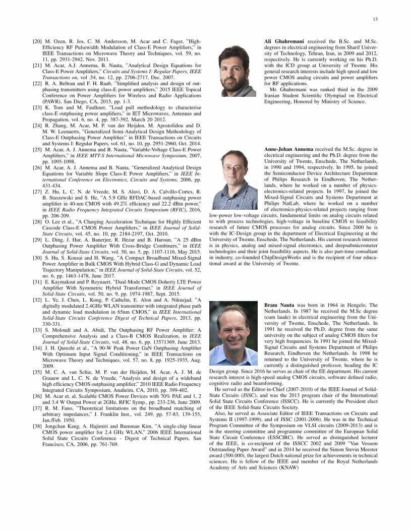
Ali Ghahremani received the B.Sc. and M.Sc.degrees in electrical engineering from Sharif Univer-sity of Technology, Tehran, Iran, in 2009 and 2012,respectively. He is currently working on his Ph.D.with the ICD group at University of Twente. Hisgeneral research interests include high speed and lowpower CMOS analog circuits and power amplifiersfor RF applications.
Mr. Ghahremani was ranked third in the 2009Iranian Student Scientific Olympiad on ElectricalEngineering, Honored by Ministry of Science.
Anne-Johan Annema received the M.Sc. degree inelectrical engineering and the Ph.D. degree from theUniversity of Twente, Enschede, The Netherlands,in 1990 and 1994, respectively. In 1995, he joinedthe Semiconductor Device Architecture Departmentof Philips Research in Eindhoven, The Nether-lands, where he worked on a number of physics-electronics-related projects. In 1997, he joined theMixed-Signal Circuits and Systems Department atPhilips NatLab, where he worked on a numberof electronics-physics-related projects ranging from
low-power low-voltage circuits, fundamental limits on analog circuits relatedto with process technologies, high-voltage in baseline CMOS to feasibilityresearch of future CMOS processes for analog circuits. Since 2000 he iswith the IC-Design group in the department of Electrical Engineering at theUniversity of Twente, Enschede, The Netherlands. His current research interestis in physics, analog and mixed-signal electronics, and deepsubmicrometertechnologies and their joint feasibility aspects. He is also part-time consultantin industry, co-founded ChipDesignWorks and is the recipient of four educa-tional award at the University of Twente.
Bram Nauta was born in 1964 in Hengelo, TheNetherlands. In 1987 he received the M.Sc degree(cum laude) in electrical engineering from the Uni-versity of Twente, Enschede, The Netherlands. In1991 he received the Ph.D. degree from the sameuniversity on the subject of analog CMOS filters forvery high frequencies. In 1991 he joined the Mixed-Signal Circuits and Systems Department of PhilipsResearch, Eindhoven the Netherlands. In 1998 hereturned to the University of Twente, where he iscurrently a distinguished professor, heading the IC
Design group. Since 2016 he serves as chair of the EE department. His currentresearch interest is high-speed analog CMOS circuits, software defined radio,cognitive radio and beamforming.
He served as the Editor-in-Chief (2007-2010) of the IEEE Journal of Solid-State Circuits (JSSC), and was the 2013 program chair of the InternationalSolid State Circuits Conference (ISSCC). He is currently the President electof the IEEE Solid-State Circuits Society.
Also, he served as Associate Editor of IEEE Transactions on Circuits andSystems II (1997-1999), and of JSSC (2001-2006). He was in the TechnicalProgram Committee of the Symposium on VLSI circuits (2009-2013) and isin the steering committee and programme committee of the European SolidState Circuit Conference (ESSCIRC). He served as distinguished lecturerof the IEEE, is co-recipient of the ISSCC 2002 and 2009 ”Van VessemOutstanding Paper Award” and in 2014 he received the Simon Stevin Meesteraward (500.000), the largest Dutch national prize for achievements in technicalsciences. He is fellow of the IEEE and member of the Royal NetherlandsAcademy of Arts and Sciences (KNAW)