1
DO-IT-YOURSELF 97 WWW.EFYMAG.COM ELECTRONICS FOR YOU | JUNE 2015 S.C. DWIVEDI Radio Frequency Detector D. MOHAN KUMAR around AM/FM detector diodes 1N34 (D1 and D2), an operational amplifier CA3130 (IC1), npn transistor BC547 (T1), connector CON1 for VU meter and a few other components. Detector diodes D1 and D2 cap- ture the RF from surroundings for the inverting input of IC1. The IC is configured as an inverting amplifier with non-inverting input tied to the negative rail. Feedback resistor R1 controls the gain of the inverting amplifier. IC CA3130 is a high-gain operational amplifier with sensitive inputs. It is a 15MHz BiMOS operational amplifier with MOSFET inputs and bipolar output. Its high-speed performance is suitable for low input-current ap- plications. RF signals are amplified by the inverting ampli- fier built around IC1. The ampli- fied signal is used to drive the sensi- tive VU meter. Potmeter VR1 is used to set zero level in the meter. When the circuit gets RF energy from a device or the surroundings, H ere is a circuit that can de- tect the presence of a radio frequency (RF) signal. If it is close to RF-emitting devices such as a television set or a computer, it shows a high reading in the UV meter, giv- ing us an idea about the intensity of RF radiation in the room. High-inten- sity RF radiation from mobile phone towers in the vicinity is considered to be harmful by most. Circuit and working The circuit diagram of the RF de- tector is shown in Fig. 1. It is built Fig. 1: Circuit diagram of the radio frequency detector Fig. 2: Actual-size PCB of the radio frequency detector Fig. 3: Component layout of the PCB D. Mohan Kumar was associate professor of Zoology (Retd) at Government College for Women, Thiruvananthapuram, Kerala PARTS LIST Semiconductors: IC1 - CA3130 operational amplifier T1 - BC547 npn transistor LED1 - 5mm LED D1-D2 - 1N34 detector diode Resistors (all 1/4-watt, ±5% carbon): R1 - 1-mega- ohm R2 - 1-kilo-ohm R3 - 470-ohm VR1 - 47-kilo-ohm potmeter Capacitors: C1-C2 - 0.22µF ceramic disk Miscellaneous: CON1 - 2-pin connector BATT.1 - 9V PP3 battery - VU meter - 8-pin IC base ANT - Telescopic antenna Fig. 4: Author’s prototype C1 0.22u R3 470E LED1 VR1 47K D1 1N34 7 8 6 5 1 4 3 2 IC1 CA3130 R1 1M R2 1K T1 BC547 D2 1N34 BATT.1 9V CON1 FOR VU METER ANT. C2 0.22u GND _ + the meter shows a deflection based on the intensity of RF. It shows full deflection when the unit is close to the RF-generating device. At the same time, transistor T1 conducts and LED1 connected to its collector glows. The glowing of LED1 depends on the in- tensity of RF; it gives full brightness when RF intensity is very high. Construction and testing An actual-size, single-side PCB for the RF detector is shown in Fig. 2 and its component layout in Fig. 3. Enclose the PCB in a suitable small box in such a way that potmeter VR1 and VU meter can be fixed on the front side. Ensure proper wiring to avoid any mistake. Do not solder CA3130 directly on the PCB; instead, use an 8-pin IC base for the IC. A telescopic antenna is used to increase the sensitivity of the circuit. Use 9V PP3 battery as the power source. Fig. 4 shows the author’s proto- type of the RF detector.

Radio Frequency Detector - electronics hobby · Radio Frequency Detector s.c. dwivedi ... level in the meter. ... BC547 npn transistor LED1 - 5mm LED D1-D2 - 1N34 detector diode

Embed Size (px)

Citation preview

do-it-yourself

97www.efymag.com electronics for you | June 2015

s.c. dwivediRadio Frequency Detector D. Mohan KuMar around AM/FM detector diodes 1N34

(D1 and D2), an operational amplifier CA3130 (IC1), npn transistor BC547 (T1), connector CON1 for VU meter and a few other components.

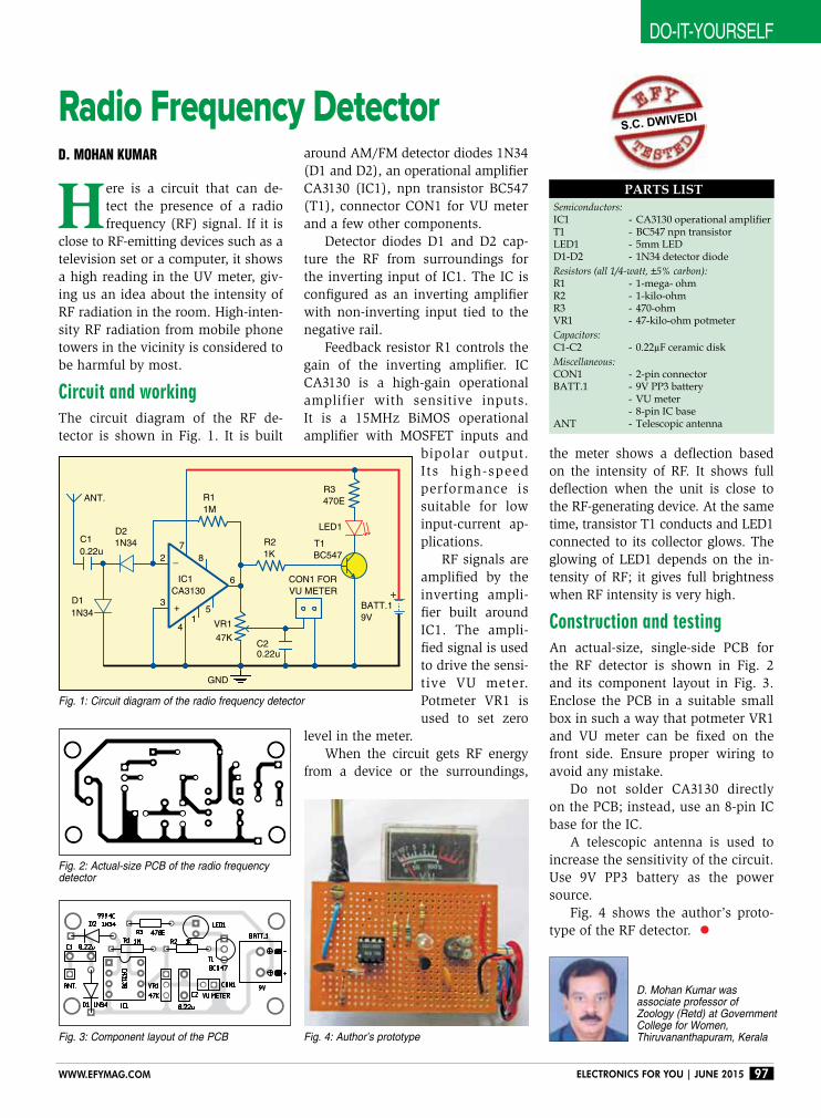
Detector diodes D1 and D2 cap-ture the RF from surroundings for the inverting input of IC1. The IC is configured as an inverting amplifier with non-inverting input tied to the negative rail.

Feedback resistor R1 controls the gain of the inverting amplifier. IC CA3130 is a high-gain operational amplifier with sensitive inputs. It is a 15MHz BiMOS operational amplifier with MOSFET inputs and

bipolar output. Its high-speed performance is suitable for low input-current ap-plications.

RF signals are amplified by the inverting ampli-fier built around IC1. The ampli-fied signal is used to drive the sensi-tive VU meter. Potmeter VR1 is used to set zero

level in the meter. When the circuit gets RF energy

from a device or the surroundings,

Here is a circuit that can de-tect the presence of a radio frequency (RF) signal. If it is

close to RF-emitting devices such as a television set or a computer, it shows a high reading in the UV meter, giv-ing us an idea about the intensity of RF radiation in the room. High-inten-sity RF radiation from mobile phone towers in the vicinity is considered to be harmful by most.

Circuit and workingThe circuit diagram of the RF de-tector is shown in Fig. 1. It is built

Fig. 1: Circuit diagram of the radio frequency detector

Fig. 2: Actual-size PCB of the radio frequency detector

Fig. 3: Component layout of the PCB

D. Mohan Kumar was associate professor of Zoology (Retd) at Government College for Women, Thiruvananthapuram, Kerala

Parts ListSemiconductors:IC1 - CA3130 operational amplifierT1 - BC547 npn transistorLED1 - 5mm LEDD1-D2 - 1N34 detector diodeResistors (all 1/4-watt, ±5% carbon):R1 - 1-mega- ohmR2 - 1-kilo-ohmR3 - 470-ohmVR1 - 47-kilo-ohm potmeterCapacitors:C1-C2 - 0.22µF ceramic diskMiscellaneous:CON1 - 2-pin connector BATT.1 - 9V PP3 battery - VU meter - 8-pin IC base ANT - Telescopic antenna

Fig. 4: Author’s prototype

C10.22u

R3470E

LED1

VR1

47K

D11N34

78

6

51

4

3

2

IC1CA3130

R11M

R21K

T1BC547

D21N34

BATT.19V

CON1 FORVU METER

ANT.

C20.22u

GND

_

+

the meter shows a deflection based on the intensity of RF. It shows full deflection when the unit is close to the RF-generating device. At the same time, transistor T1 conducts and LED1 connected to its collector glows. The glowing of LED1 depends on the in-tensity of RF; it gives full brightness when RF intensity is very high.

Construction and testingAn actual-size, single-side PCB for the RF detector is shown in Fig. 2 and its component layout in Fig. 3. Enclose the PCB in a suitable small box in such a way that potmeter VR1 and VU meter can be fixed on the front side. Ensure proper wiring to avoid any mistake.

Do not solder CA3130 directly on the PCB; instead, use an 8-pin IC base for the IC.

A telescopic antenna is used to increase the sensitivity of the circuit. Use 9V PP3 battery as the power source.

Fig. 4 shows the author’s proto-type of the RF detector.