Embed Size (px)
Citation preview

R02DS0017EJ0100 Rev.1.00 Page 1 of 75 Apr. 9, 2018
Data Sheet
RAA270005KFP General Purpose Power Management IC
Description The RAA270005KFP is a general-purpose Power Management IC (PMIC), and suitable for RENESAS RH850/P1x series microcontroller (MCU). The features and the details of the PMIC are described in this document. The PMIC contains two types of DCDCs converters: buck and boost, two low dropout linear regulators (LDO) and two linear trackers. The switching frequency of boost/buck DCDCs are typical 420 kHz, 2.1 MHz respectively. Monitor functions for the internal status are implemented. Input voltage, output of all regulators, and internal analog voltage corresponding to temperature can be monitored through ADC of MCU. And reference voltage can be monitored for testing the ADC of MCU as well. The PMIC has sequencer circuits for controlling power-up/down, therefore any external sequencer circuits are unnecessary. And the PMIC can control an external backup-power for MCU.
Features • Supply the power to Renesas RH850/P1x (eVR)
• Load dump robustness
• Input voltage range: 6.6~18.5V to perform specified characteristics. 5.4V~: continued operation without low voltage detection 3.8V~: continued operation declined the output voltage * If not use the boost DCDC converter
• DCDC converter: Boost: 6.0V/250mA (Input voltage: 2.2V~) Buck: 6.1V/600mA
• Linear regulators: 1. Output voltage : 3.3V/10mA 2. Output voltage : 5.0V/350mA with reverse protection
• Two linear trackers Output voltage: VOUT1/100mA with reverse protection
• Automatic power sequence
• An external backup-power control
• Watchdog timer
• Analog multiplexer
• Interrupt request
• Thermal shut down
• Reset generator
• External devices control
• Monitoring to a core voltage in MCU.
• Exposed die pad, HLQFP package, 40pin 9mm x 9mm
Application • Automotive applications
• Industrial applications
R02DS0017EJ0100
Rev.1.00
Apr. 9, 2018

RAA270005KFP
R02DS0017EJ0100 Rev.1.00 Page 2 of 75 Apr. 9, 2018
Table of Contents 1. Abusolute maximum ratings ............................................................................................ 4 2. Pin Configuration ............................................................................................................. 5
2.1. Pin Configuration ...................................................................................................... 5 2.2. Pin list ....................................................................................................................... 6
3. Internal Block Diagram .................................................................................................... 8 4. PMIC Function ............................................................................................................... 10
4.1. Abstract of the PMIC ............................................................................................... 10 4.1.1. PMIC Operation .............................................................................................. 10 4.1.2. Pin setting ....................................................................................................... 11 4.1.3. Configuration register ..................................................................................... 12 4.1.4. Product code ................................................................................................... 12
4.2. Serial Interface ........................................................................................................ 13 4.2.1. Signal format ................................................................................................... 13 4.2.2. Ensuring communication ................................................................................ 14 4.2.3. Secured request ............................................................................................. 15 4.2.4. Register ........................................................................................................... 15 4.2.5. Register map ................................................................................................... 16 4.2.6. Electrical characteristics ................................................................................. 17
4.3. Reference Voltage .................................................................................................. 18 4.3.1. Electrical characteristics ................................................................................. 18
4.4. LDO ......................................................................................................................... 19 4.4.1. Output protection function .............................................................................. 20 4.4.2. Electrical characteristics ................................................................................. 20
4.5. Tracker .................................................................................................................... 21 4.5.1. Register ........................................................................................................... 22 4.5.2. Electrical characteristics ................................................................................. 22
4.6. DCDC converter (DCDC) ....................................................................................... 23 4.6.1. Buck DCDC ..................................................................................................... 23 4.6.2. Boost DCDC ................................................................................................... 24 4.6.3. Register ........................................................................................................... 26 4.6.4. Electrical characteristics ................................................................................. 27
4.7. Power Rail Sequence ............................................................................................. 28 4.7.1. Power up sequence ........................................................................................ 28 4.7.2. Power down sequence ................................................................................... 29 4.7.3. Working with a backup-power ........................................................................ 31
4.8. Watchdog Timer (WDT) .......................................................................................... 33 4.8.1. Window WDT .................................................................................................. 33 4.8.2. WDT operation ................................................................................................ 33 4.8.3. Advanced mode .............................................................................................. 36 4.8.4. Register ........................................................................................................... 38 4.8.5. Electrical characteristic ................................................................................... 40
4.9. Reset ....................................................................................................................... 41 4.9.1. Reset factor ..................................................................................................... 41 4.9.2. Reset factor register ....................................................................................... 42 4.9.3. Software reset ................................................................................................. 43 4.9.4. External reset .................................................................................................. 43 4.9.5. Electrical characteristics ................................................................................. 44
4.10. Specified output pins ........................................................................................... 45 4.10.1. Low voltage indicator (SUSP) .................................................................... 45 4.10.2. Error input (ERROR) .................................................................................. 45 4.10.3. External control (EXCNT1/2) ..................................................................... 46 4.10.4. Backup-power control (BKCNT) ................................................................ 48 4.10.5. Register ...................................................................................................... 49 4.10.6. Electrical characteristics ............................................................................ 50
4.11. Interrupt Signal .................................................................................................... 51 4.11.1. Interrupt control .......................................................................................... 51 4.11.2. Interrupt factors .......................................................................................... 51

RAA270005KFP
R02DS0017EJ0100 Rev.1.00 Page 3 of 75 Apr. 9, 2018
4.11.3. Register ...................................................................................................... 52 4.12. Functional Safety ................................................................................................. 59
4.12.1. Voltage detection ....................................................................................... 59 4.12.2. PMIC behavior after unusual detection ..................................................... 60 4.12.3. Self-diagnosis ............................................................................................ 61 4.12.4. Electrical characteristics ............................................................................ 62
4.13. Temperature sensor ............................................................................................ 65 4.13.1. Thermal shutdown ..................................................................................... 65 4.13.2. Register ...................................................................................................... 65
4.14. Monitoring Function ............................................................................................. 67 4.14.1. Internal analog voltage monitoring ............................................................ 67 4.14.2. Digital output monitoring ............................................................................ 67 4.14.3. Register ...................................................................................................... 68 4.14.4. Electrical characteristics ............................................................................ 68
5. Application Example ...................................................................................................... 71 5.1. Layout guide lines ................................................................................................... 73
6. Electrical Characteristics ............................................................................................... 74 6.1. Recommended operating condition ........................................................................ 74 6.2. Electrical characteristics ......................................................................................... 74
6.2.1. DC characteristics ........................................................................................... 74 7. Package Information ...................................................................................................... 75
RAA270005KFP
R02DS0017EJ0100 Rev.1.00 Page 4 of 75 Apr. 9, 2018
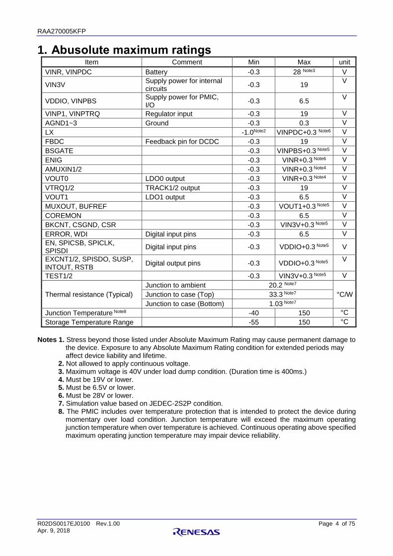
1. Abusolute maximum ratings Item Comment Min Max unit
VINR, VINPDC Battery -0.3 28 Note3 V
VIN3V Supply power for internal circuits
-0.3 19 V
VDDIO, VINPBS Supply power for PMIC, I/O
-0.3 6.5 V
VINP1, VINPTRQ Regulator input -0.3 19 V
AGND1~3 Ground -0.3 0.3 V
LX -1.0Note2 VINPDC+0.3 Note6 V
FBDC Feedback pin for DCDC -0.3 19 V
BSGATE -0.3 VINPBS+0.3 Note5 V
ENIG -0.3 VINR+0.3 Note6 V
AMUXIN1/2 -0.3 VINR+0.3 Note4 V
VOUT0 LDO0 output -0.3 VINR+0.3 Note4 V
VTRQ1/2 TRACK1/2 output -0.3 19 V
VOUT1 LDO1 output -0.3 6.5 V
MUXOUT, BUFREF -0.3 VOUT1+0.3 Note5 V
COREMON -0.3 6.5 V
BKCNT, CSGND, CSR -0.3 VIN3V+0.3 Note5 V
ERROR, WDI Digital input pins -0.3 6.5 V
EN, SPICSB, SPICLK, SPISDI
Digital input pins -0.3 VDDIO+0.3 Note5 V
EXCNT1/2, SPISDO, SUSP, INTOUT, RSTB
Digital output pins -0.3 VDDIO+0.3 Note5 V
TEST1/2 -0.3 VIN3V+0.3 Note5 V
Thermal resistance (Typical)
Junction to ambient 20.2 Note7
°C/W Junction to case (Top) 33.3 Note7
Junction to case (Bottom) 1.03 Note7
Junction Temperature Note8 -40 150 °C
Storage Temperature Range -55 150 °C
Notes 1. Stress beyond those listed under Absolute Maximum Rating may cause permanent damage to
the device. Exposure to any Absolute Maximum Rating condition for extended periods may affect device liability and lifetime.
2. Not allowed to apply continuous voltage. 3. Maximum voltage is 40V under load dump condition. (Duration time is 400ms.)
4. Must be 19V or lower. 5. Must be 6.5V or lower. 6. Must be 28V or lower. 7. Simulation value based on JEDEC-2S2P condition. 8. The PMIC includes over temperature protection that is intended to protect the device during
momentary over load condition. Junction temperature will exceed the maximum operating junction temperature when over temperature is achieved. Continuous operating above specified maximum operating junction temperature may impair device reliability.

RAA270005KFP
R02DS0017EJ0100 Rev.1.00 Page 5 of 75 Apr. 9, 2018
2. Pin Configuration
Pin configuration is shown in the below figure. The package is 40pin exposed die pad HLQFP.
Figure 2-1 Pin configuration (Top view)
1 10
11
20
21
31
40
BK
CN
T
AM
UX
IN1
TE
ST
2
EN
IG
VIN
R
VIN
PD
C
LX
AG
ND
1
FB
DC
ER
RO
R
COREMON
AGND2
INTOUT
VDDIO
SPISDO
SPICLK
SPICSB
SPISDI
RSTB
EN
BU
FR
EF
VT
RQ
2
AM
UX
IN2
VIN
PT
RQ
VT
RQ
1
MU
XO
UT
VO
UT
1
SU
SP
WD
I
VIN
P1
EXCNT1
EXCNT2
VINPBS
CSGND
CSR
AGND3
BSGATE
TEST1
VIN3V
VOUT0
30

RAA270005KFP
R02DS0017EJ0100 Rev.1.00 Page 6 of 75 Apr. 9, 2018
The pin list table is shown below.
Re
ma
rks
Co
nn
ect
to G
rou
nd
Inclu
de
d p
ull-
do
wn
resis
tor
Co
nn
ect
to b
atte
ry
Co
nn
ect
to b
atte
ry
Inclu
de
d p
ull-
do
wn
resis
tor
Inclu
de
d p
ull-
do
wn
resis
tor
Inclu
de
d p
ull-
up r
esis
tor
Inclu
de
d p
ull-
do
wn
resis
tor
Inclu
de
d p
ull-
up r
esis
tor
Inclu
de
d p
ull-
do
wn
resis
tor
Pro
tect circuit
GN
D n
am
e
AG
ND
1
AG
ND
3
AG
ND
1
AG
ND
1
AG
ND
1
AG
ND
1
AG
ND
1
-
AG
ND
1
AG
ND
1
AG
ND
1
AG
ND
1
AG
ND
2
AG
ND
2
AG
ND
2
AG
ND
2
AG
ND
2
AG
ND
2
-
AG
ND
2
VD
D n
am
e
VIN
3V
-
VIN
3V
VIN
R
- - - - - -
VD
DIO
VD
DIO
VD
DIO
VD
DIO
VD
DIO
VD
DIO
-
VD
DIO
- -
Inte
rface
level
CM
OS
- -
NM
OS
- - - - - -
CM
OS
Op
en
dra
in
CM
OS
CM
OS
CM
OS
CM
OS
-
CM
OS
- -
I/O
/P/G
Ou
tpu
t
Inp
ut
-
Inp
ut
Po
wer
Po
wer
Ou
tpu
t
-
Inp
ut
Inp
ut
Inp
ut
Ou
tpu
t
Inp
ut
Inp
ut
Inp
ut
Ou
tpu
t
Po
wer
Ou
tpu
t
-
Inp
ut
An
alo
g/
Dig
ital
Dig
ital
An
alo
g
-
Dig
ital
- -
An
alo
g
-
An
alo
g
Dig
ital
Dig
ital
Dig
ital
Dig
ital
Dig
ital
Dig
ital
Dig
ital
-
Dig
ital
-
An
alo
g
Pin
fu
nctio
n
Ba
cku
p-p
ow
er
con
trol
An
alo
g m
ultip
lexe
r in
pu
t1
Fo
r te
st
Po
wer
en
ab
le o
f th
e P
MIC
Po
wer
sup
ply
fo
r L
DO
0
Bu
ck D
CD
C in
pu
t
Dri
ve
r ou
tput
for
an
exte
rna
l in
du
cto
r
Gro
un
d
Bu
ck D
CD
C fee
d-b
ack inp
ut
Mo
nito
rin
g in
pu
t fr
om
MC
U
Po
wer
en
ab
le o
f th
e P
MIC
Rese
t o
utp
ut
Se
ria
l in
terf
ace
, da
ta in
put
Se
ria
l in
terf
ace
, ch
ip s
ele
ct
Se
ria
l in
terf
ace
, clo
ck in
pu
t
Se
ria
l in
terf
ace
, da
ta o
utp
ut
Po
wer
sup
ply
fo
r d
igital IO
pa
rt o
f th
e P
MIC
Inte
rrup
t sig
na
l ou
tpu
t
Gro
un
d
Mo
nito
rin
g t
o a
co
re v
olta
ge in M
CU
Pin
nam
e
BK
CN
T
AM
UX
IN1
TE
ST
2
EN
IG
VIN
R
VIN
PD
C
LX
AG
ND
1
FB
DC
ER
RO
R
EN
RS
TB
SP
ISD
I
SP
ICS
B
SP
ICL
K
SP
ISD
O
VD
DIO
INT
OU
T
AG
ND
2
CO
RE
MO
N
Pin
#
1
2
3
4
5
6
7
8
9
10
11
12
13
14
15
16
17
18
19
20

RAA270005KFP
R02DS0017EJ0100 Rev.1.00 Page 7 of 75 Apr. 9, 2018
Pin list (Continued) R
em
ark
s
Inclu
de
d p
ull-
do
wn
resis
tor
Co
nn
ect
to 0
.1μ
F
De
tectio
n r
esis
tor,
lo
w v
olta
ge s
ide
De
tectio
n r
esis
tor,
hig
h v
olta
ge
sid
e
Exte
rna
l tr
an
sis
tor
co
ntr
ol
Co
nn
ect
to g
roun
d
Pro
tect circuit
GN
D n
am
e
AG
ND
2
AG
ND
2
AG
ND
2
AG
ND
2
AG
ND
2
AG
ND
2
AG
ND
2
AG
ND
3
AG
ND
2
AG
ND
2
AG
ND
3
AG
ND
3
AG
ND
3
AG
ND
3
AG
ND
3
-
AG
ND
3
AG
ND
1
AG
ND
3
AG
ND
3
VD
D n
am
e
- -
VD
DIO
-
VO
UT
1
- - - - -
VD
DIO
VD
DIO
- - - -
VIN
PB
S
VIN
3V
-
VIN
R
Inte
rface
level
-
CM
OS
CM
OS
- - - - - - -
CM
OS
CM
OS
- - - - - - - -
I/O
/P/G
Po
wer
Inp
ut
Ou
tpu
t
Ou
tpu
t
Ou
tpu
t
Ou
tpu
t
Po
wer
Inp
ut
Ou
tpu
t
Ou
tpu
t
Ou
tpu
t
Ou
tpu
t
Po
wer
Inp
ut
Inp
ut
-
Ou
tpu
t
-
Po
wer
Ou
tpu
t
An
alo
g/
Dig
ital
-
Dig
ital
Dig
ital
An
alo
g
An
alo
g
An
alo
g
-
An
alo
g
An
alo
g
An
alo
g
Dig
ital
Dig
ital
-
An
alo
g
An
alo
g
-
An
alo
g
- -
An
alo
g
Pin
fu
nctio
n
Po
wer
sup
ply
fo
r L
DO
1
Cle
ar
wa
tch
do
g tim
er
Lo
w v
olta
ge
ind
ica
tor
of
LD
O1
LD
O1
ou
tpu
t
An
alo
g m
ultip
lexe
r ou
tput
TR
AC
K1 o
utp
ut
Po
wer
sup
ply
fo
r T
RA
CK
2
An
alo
g m
ultip
lexe
r in
pu
t2
TR
AC
K2 o
utp
ut
Refe
rence
vo
lta
ge
ou
tpu
t
Sp
ecifie
d d
igital o
utp
ut1
Sp
ecifie
d d
igital o
utp
ut2
Po
wer
sup
ply
fo
r b
oost
DC
DC
Curr
en
t de
tection
1 fo
r b
oo
st
DC
DC
Curr
en
t de
tection
2 fo
r b
oo
st
DC
DC
Gro
un
d
Bo
ost sw
itch
ing
co
ntr
ol
Fo
r te
st
Po
wer
sup
ply
fo
r th
e in
tern
al cir
cu
it
LD
O0
ou
tpu
t
Pin
nam
e
VIN
P1
WD
I
SU
SP
VO
UT
1
MU
XO
UT
VT
RQ
1
VIN
PT
RQ
AM
UX
IN2
VT
RQ
2
BU
FR
EF
EX
CN
T1
EX
CN
T2
VIN
PB
S
CS
GN
D
CS
R
AG
ND
3
BS
GA
TE
TE
ST
1
VIN
3V
VO
UT
0
Pin
#
21
22
23
24
25
26
27
28
29
30
31
32
33
34
35
36
37
38
39
40

RAA270005KFP
R02DS0017EJ0100 Rev.1.00 Page 8 of 75 Apr. 9, 2018
3. Internal Block Diagram The PMIC block diagram is shown in the below figure.
Figure 3-1 The PMIC block diagram
BGR
LDO0
LDO1
OSC
SPI I/F
WDT
Internal power
VINR
VOUT0
VIN3V
ENIG
EN
SUSP
ERROR
BKCNT
EXCNT1
EXCNT2
SPICSB SPICLK
SPISDI
SPISDO
WDI
Buck DCDC
MUXOUT
AMUXIN1
AMUXIN2
VINPDC
LX FBDC
VINP1 VOUT1
VINPTRQ VTRQ1
BUFREF
VDDIO
VREF
Operation Control
RSTB Sequencer
Analog
Multiplexer
Thermal Shut-down
Interrupt
Control INTOUT
VTRQ2 TRACK2
TRACK1
Core voltage
Monitor COREMON
TEST1
TEST2
Boost DCDC
VINPBS BSGATE
CSR
CSGND
VDDIO

RAA270005KFP
R02DS0017EJ0100 Rev.1.00 Page 9 of 75 Apr. 9, 2018
The abstractive descriptions are here. Refer to each section for more details. Boost DCDC
Boost DCDC is a switching regulator which boost up to 6.0V, and the frequency is 420 kHz. LDO0
LDO0 is a low drop output regulator which generates 3.3V power. The output current ability is 10mA. LDO1
LDO1 is a low drop output regulator which generates 5.0V power. The output current ability is 350mA. TRACK1
TRACK1 is a voltage tracker. The output tracks a voltage applied on VOUT1. The current ability is 100mA.
TRACK2 TRACK1 is a voltage tracker. The output tracks a voltage applied on VOUT1. The current ability is 100mA.
Buck DCDC Buck DCDC is a switching regulator which generates 6.1V, and the frequency is 2.1 MHz. The output current ability is 600mA.
Band gap reference (BGR) BGRs generate reference voltages for each regulator.
VREF VREF generates reference voltages for regulators. An external capacitor is necessary to reduce noise of LDO1.
Analog multiplexer An analog multiplexer outputs internal analog voltage of the PMIC or external pins (AMUXIN1/2).
SPI interface SPI receives requests from MCU, or sends register setting.
Watch dog timer (WDT) WDT monitors system operating, can be controlled by WDI pin or via SPI.
Sequencer Sequencer controls power up/down of the regulators.
Operation control Operation control for the PMIC and external pins.
Interrupt control Interrupt operation control.
Oscillator Oscillator for sequencer, buck DCDC and boost DCDC.
Thermal shutdown Thermal shutdown monitors the temperature in the PMIC. If the internal temperature exceeds the shutdown temperature, the PMIC goes to P/D sequence2.
Core voltage monitor Core voltage monitor detects the under or over voltage of MCU’s core voltage.

RAA270005KFP
R02DS0017EJ0100 Rev.1.00 Page 10 of 75 Apr. 9, 2018
4. PMIC Function
In order to supply power to MCU or ASIC, the PMIC contains current mode DCDC converters (DCDC) and two LDOs. The buck DCDC’s output is used for LDO1’s or trackers power source. When a battery voltage is applied to the PMIC, the regulators rise up automatically in accordance with designated sequence. And after all outputs of the regulators power up successfully, the “INTOUT” signal is released. The PMIC also has a watchdog timer (WDT). When timer in the WDT expires, a reset signal is occurred. The WDT is refreshed by a request via WDI pin or SPI. When the junction temperature reaches over Tsd, a reset occurs and the all regulators except for LDO0 is forced to power down immediately
4.1.1. PMIC Operation The principal operate transitions and conditions are illustrated in the below state diagram. ENIG or EN is enables operation of the PMIC.
Figure 4-1 State diagram
Power down
Stand-by RSTB=L
P/U sequence
Self-diagnosis
ENIG=0 & EN=0
Tj < Trls
ENIG=0 & EN=0
Cool down
ENIG=0 & EN=0
ENIG or EN=1
Reset1
Reset2
P/D sequence2
P/D sequence1
Tj < Trls
Tj > Tsd
COREMON < Vdcol2 or
Tj > Tsd
COREMON < Vdcol2 or Tj > Tsd
Normal RSTB=H
ENIG=1 & (VINR > Vrbu)
(ENIG=0 & EN=0) or VINR < Vdbu
(ENIG=0 & EN=0) or VOUT1 < Vd1l2

RAA270005KFP
R02DS0017EJ0100 Rev.1.00 Page 11 of 75 Apr. 9, 2018
Power down In this state, no blocks in the PMIC operate.
Stand-by In this state, the PMIC executes initial reset of internal registers and RSTB pin is asserted low. Only LDO0 is activated by ENIG=1 operates in this state.
Self-diagnosis Self-diagnostic automatically is started after stand-by state. In this state, over/low voltage detector in the regulators, the temperature sensor and the internal logic circuit are checked.
P/U sequence After executing self-diagnostic, this state is automatically entered. Even if one of regulators doesn’t rise up, the PMIC stays in this state. After LDO1 rise up, INTOUT is high and passed 14.5ms, a reset is released.
Normal After the reset is released, this state is automatically entered. The system monitor is started with using the WD function. And also, the PMIC monitors the junction temperature and the output voltage of VOUT1.
Reset1b RSTB asserts low by setting low both ENIG and EN, or low voltage detection of VOUT1 immediately.
P/D sequence1 This state is automatically entered after “Reset 1” state. Buck DCDC and LDO1 start to fall down in designated order. The junction temperature is checked. If the junction temperature is higher than Tsd, then the PMIC enters “Cool down” state. If lower than Trls, the PMIC enters back “Stand-by” state.
Reset2 When the junction temperature comes over Tsd or the low voltage of core voltage is detected, the reset is released.
P/D sequence2 This state is automatically entered after “Reset2” state. Buck DCDC and LDO1 start to fall down in designated order. When ENIG or EN is set to high, the PMIC goes to “Cool down” state. When ENIG and EN are set to low, the PMIC goes to “Stand-by” state.
Cool down The PMIC checks if the junction temperature is lower than Trls. If the junction temperature is higher than Tsd, the PMIC waits until the junction temperature cools down. After the junction temperature comes below Trls, the PMIC enters “Stand-by” state. When ENIG and EN are set to low, the PMIC also goes to “Stand-by” state.
4.1.2. Pin setting The PMIC has ENIG and EN pin to define PMIC operation. For proper operation, these pins should be set to the appropriate level. The appropriate setting voltages are described in “6. Electrical Characteristics” PMIC enabling
The PMIC enabling is set by ENIG or EN pin. And in the initial phase, the PMIC should be enabled on by ENIG. ENIG pin can be connected to a battery voltage.
Table 4-1 PMIC operation setting
ENIG EN PMIC operation
0 0 PMIC disable
0 1 PMIC enable
1 0 PMIC enable
1 1 PMIC enable

RAA270005KFP
R02DS0017EJ0100 Rev.1.00 Page 12 of 75 Apr. 9, 2018
4.1.3. Configuration register In order to configure function of the PMIC, need to set in this register. Refer to each described section for more setting information. Configuration register
The below registers are secured registers. Enter “key” code, before entering this request. (Refer to section 4.2.3.) Address (CONF): 10H
A5 A4 A3 A2 A1 A0
0 1 0 0 0 0
Register
D7 D6 D5 D4 D3 D2 D1 D0
- - - RSTMD - RSTERR SPIWDT ADVWD
Setting contents
Register name Control contents Setting
1 0
RSTMD D4 Reset mode L Pulse *
RSTERR D2 Reset assertion by ERROR On Off *
SPIWDT D1 Select WDT clear input channel SPI WDI *
ADVWD D0 Advanced mode for WD operating On Off *
* Default setting Note: Advanced mode for WD is effective when SPI is selected to refresh WDT.
RSTMD: Reset mode select when a reset is occurred. RSTERR: Reset control register by ERROR. After setting “On”, RSTB asserts low when ERROR
indicates error. SPIWDT: select WDT clear input ADVWD: This register can set to operate WDT in advanced mode. After setting “Enable”, WD
operates in advanced mode. Refer to section 4.8.3.
4.1.4. Product code These bits identify the PMIC product code. Product code Address(CHIPID): 00H
A5 A4 A3 A2 A1 A0
0 0 0 0 0 0
Register (Read only)
D7 D6 D5 D4 D3 D2 D1 D0
1 0 0 0 0 0 1 0

RAA270005KFP
R02DS0017EJ0100 Rev.1.00 Page 13 of 75 Apr. 9, 2018
The PMIC includes serial to peripheral interface (SPI). Refer to each section for more detail contents, WDT operation (If SPI control is selected) Control the monitor function Reset control, read reset factor, write reset clear/mask Interrupt control, read interrupt factor, write interrupt clear/mask Tracker control Change thermal detection
4.2.1. Signal format The bit length of the communication is 16bits, and the signal format is illustrated in below figures. The data should be transmitted as MSB first. For this SPI, one SPICSB active is for one request. Therefore, SPICSB should be high after transmitted data.
Figure 4-2 SPI format (Write)
Figure 4-3 SPI format (Read)
Caution: The entered data is latched by rising edge of SPICSB.
W A5 A4 A3 A2 A1 A0 D7 D6 D5 D4 D3 D2 D1 D0 P Invalid
SPICSB
SPICLK
SPISDI SPISDO
Hi-Z Hi-Z
R A5 A4 A3 A2 A1 A0 Invalid
Hi-Z Do7 Do6 Do5 Do4 Do3 Do2 Do1 Do0 P
SPICSB
SPICLK
SPISDI SPISDO
Hi-Z
RAA270005KFP
R02DS0017EJ0100 Rev.1.00 Page 14 of 75 Apr. 9, 2018
W/R This bit indicates write or read register. To write register, bit W/R should be set 0. To read register, bit W/R should be set 1. When read register, Do7-Do0 bits indicate contents. (D7-D0 bits are ignored in the PMIC.)
A5-A0 The PMIC contains several registers. The addresses are described in these bits. Every register can be read to confirm its content.
D7-D0 These bits describe control bits of the PMIC to write into the PMIC.
Do7-Do0 These bits describe content bits or flag bits to read from the PMIC. SPISDO pin keeps Hi-z during transmitting “W/R” bit and address bits, A5-A0. The parity bit of read data is calculated with “W/R” bit and all address bits as 1.
P This bit indicates a parity bit calculated based on the number of logic contained in bits excepting parity bit itself.
Bit P has to be set 0 if the number of 1 is odd. Bit P has to be set 1 if the number of 1 is even. Note: If interrupt factors of the target address occurs during the interrupt factor reading, the parity bit might not be set correctly.
4.2.2. Ensuring communication To ensure the communication between the PMIC and MCU, the PMIC observes the SPI signal of following accesses. If any violation, The PMIC ignores this command or request. Number of SPICLK
The PMIC counts SPICLK clocks while SPICSB is low. If the number of clock is not 16, that communication is considered as an error. The PMIC ignores this command or request.
Undefined address When undefined address is transmitted, the PMIC ignores this address’ contents.
Parity bit The SPI format includes a parity bit. The PMIC monitors the parity bit and if transmitted bits are not based on the parity bit, this communication is considered as an error. The PMIC ignores this command or request.

RAA270005KFP
R02DS0017EJ0100 Rev.1.00 Page 15 of 75 Apr. 9, 2018
4.2.3. Secured request A MCU read PRTCT register to get key and write it back to PRTCT register before modifying those secured registers, instead of writing the key to those secured registers. Without the key code, the request is ignored. Pin setting (Address: 02H) Interrupt mask register (Address: 0CH~0FH) Configuration register (Address: 10H) Reset mask register (Address: 14H) Window time setting for WDT (Address: 17H) Tracker register (Address: 1AH) Buck DCDC protection setting (Address: 1BH) Software reset (Address: 1DH) Temperature setting for the thermal shut down (Address: 1EH) Boost DCDC protection setting (Address: 1FH)
Figure 4-4 Key code unlock
4.2.4. Register The contents of SPI setting are described in this section. Protect deactivate key code Address (PRTCT): 11H
A5 A4 A3 A2 A1 A0
0 1 0 0 0 1
Register Before the access secured registers, need to obtain the below random code by read mode.
Do7 Do6 Do5 Do4 Do3 Do2 Do1 Do0
RDMKEY (Do7:Do0)
Need to enter the obtained data before MCU enters request.
D7 D6 D5 D4 D3 D2 D1 D0
RDMKEY (D7:D0)
Setting contents
• RDMO (Do7:Do0): Random code from the PMIC
• RDMI (D7:D0): Copy and sent RDMO (Do7:Do0)
RSTB
SPICSB
PRTCT (Read)
SPISDO
SPISDI PRTCT Add. RDMKEY
RDMKEY
Read Keycode
Data
Write same value

RAA270005KFP
R02DS0017EJ0100 Rev.1.00 Page 16 of 75 Apr. 9, 2018
4.2.5. Register map The registers which can be set in the PMIC are summarized in below table with its address and data. The detail contents are described in each section. Hexadecimal number is written as xxH.
Note: The initial value of PRTCT, WDTRG are undefined value.
Ad
dre
ss
Re
gis
ter
Na
me
R/W
D7
D6
D5
D4
D3
D2
D1
D0
Init
ial
Se
cu
red
Re
set
by
Fu
ncti
on
00H
CH
IPID
R82H
C
hip
ID
02H
SE
TD
PIN
R/W
---
---
---
---
SE
TE
XC
NT
2S
ET
EX
CN
T1
SE
TS
US
PS
ET
BK
CN
T02H
R
STB
S
et
/ R
ead for
dig
ital outp
ut
pin
s
03H
INTF
AC
R--
---
-IN
TR
SF
GIN
TS
DIN
TR
4IN
TR
3IN
TR
2IN
TR
100H
DE
T0O
In
terr
upt
facto
r
04H
INTR
EQ
1R
DE
TT
RQ
2O
CD
ET
TR
Q1
OC
DE
TB
SO
CD
ET
CO
LD
ET
TR
Q2
LD
ET
TR
Q1
LD
ET
1L
DE
TD
CL
00H
DE
T0O
In
terr
upt
request
1
05H
INTR
EQ
2R
---
---
DE
TC
OU
2D
ET
CO
U1
DE
TT
RQ
2U
DE
TT
RQ
1U
DE
T1
UD
ET
DC
U00H
DE
T0O
In
terr
upt
request
2
06H
INTR
EQ
3R
BK
MO
DE
SD
BK
UP
SD
ST
AS
DO
SC
BA
TB
KD
ET
RE
FW
RT
MP
DE
TD
CO
C00H
DE
T0O
In
terr
upt
request
3
07H
INTR
EQ
4R
DU
MM
Y--
---
-P
EX
CN
T2
PE
XC
NT
1P
SU
SP
PB
KC
NT
PR
ST
B00H
DE
T0O
In
terr
upt
request
4
08H
INTC
L1
WC
LT
RQ
2O
CC
LT
RQ
1O
CC
LB
SO
CC
LC
OL
CL
TR
Q2
LC
LT
RQ
1L
CL
1L
CL
DC
L-
RS
TB
In
terr
upt
cle
ar
1
09H
INTC
L2
W--
---
-C
LC
OU
2C
LC
OU
1C
LT
RQ
2U
CL
TR
Q1
UC
L1
UC
LD
CU
-R
STB
In
terr
upt
cle
ar
2
0A
HIN
TC
L3
WC
LB
KM
OD
EC
LB
KU
PC
LS
DS
TA
CL
SD
OS
CC
LB
AT
BK
CL
RE
FC
LW
RT
MP
CL
DC
OC
-R
STB
In
terr
upt
cle
ar
3
0B
HIN
TC
L4
W--
---
---
-C
LP
EX
CN
T2
CL
PE
XC
NT
1C
LP
SU
SP
CL
PB
KC
NT
CL
PR
ST
B-
RS
TB
In
terr
upt
cle
ar
4
0C
HIN
TM
SK
1R
/WM
SK
TR
Q2
OC
MS
KT
RQ
1O
CM
SK
BS
OC
---
MS
KT
RQ
2L
MS
KT
RQ
1L
MS
K1
LM
SK
DC
L00H
R
STB
In
terr
upt
mask 1
0D
HIN
TM
SK
2R
/W--
---
-M
SK
CO
U2
MS
KC
OU
1M
SK
TR
Q2
UM
SK
TR
Q1
UM
SK
1U
MS
KD
CU
00H
R
STB
In
terr
upt
mask 2
0E
HIN
TM
SK
3R
/W--
---
-M
SK
SD
ST
AM
SK
SD
OS
C--
-M
SK
RE
FM
SK
WR
TM
PM
SK
DC
OC
00H
R
STB
In
terr
upt
mask 3
0F
HIN
TM
SK
4R
/W--
---
---
-M
SK
PE
XC
NT
2M
SK
PE
XC
NT
1M
SK
PS
US
PM
SK
PB
KC
NT
MS
KP
RS
TB
00H
R
STB
In
terr
upt
mask 4
10H
CO
NF
R/W
---
---
---
RS
TM
D--
-R
ST
ER
RS
PIW
DT
AD
VW
D00H
D
ET0O
C
onfig
ura
tion r
egis
ter
11H
PR
TC
TR
/W**
HR
STB
P
rote
ct
rem
ove
code
12H
RS
TF
AC
R--
-S
TP
ER
RO
VA
DV
LV
CO
RE
TS
DT
MP
WD
EX
PW
DS
US
LV
LD
O1
00H
DE
T0O
R
eset
facto
r
13H
RS
TF
CL
W--
-C
LS
TP
ER
RC
LO
VA
DV
CL
LV
CO
RE
CL
TS
DT
MP
CL
WD
EX
PC
LW
DS
US
CL
LV
LD
O1
-R
STB
R
eset
facto
r cle
ar
14H
RS
TF
MS
KR
/W--
---
-M
SK
OV
AD
V--
-M
SK
TS
DT
MP
MS
KW
DE
XP
MS
KW
DS
US
---
00H
R
STB
R
eset
facto
r m
ask
15H
PIN
SE
TR
/W--
---
---
---
-S
EL
DT
ER
MO
DE
00H
RS
TB
E
XC
NT a
nd e
rror
monitor
sett
ing
16H
WD
TR
GR
/W**
HR
STB
W
D a
dva
nced m
ode
17H
WD
TIM
ER
/W--
---
---
---
-01H
R
STB
W
D w
indow
tim
e s
ett
ing
18H
MU
XC
NT
R/W
---
MU
XC
NT
---
---
00H
RS
TB
M
uxam
p c
ontr
ol
19H
QA
EV
AR
00H
RS
TB
A
ccum
ula
ted v
alu
e for
WD
adva
nced m
ode
1A
HTR
QC
NT
R/W
---
---
---
TR
QL
VS
EL
---
---
VT
RQ
2C
NT
VT
RQ
1C
NT
00H
R
STB
TR
AC
K1/2
on/o
ff contr
ol
1B
HD
CLIM
R/W
---
---
---
---
04H
D
ET0O
Lim
it c
ontr
ol fo
r D
CD
C
1C
HR
STV
AR
/WF
FH
RS
TB
N
um
ber
of re
set
for
WD
adva
nced m
ode
1D
HS
FTR
ST
W-
R
STB
S
oftw
are
reset
1E
HS
EN
TM
PR
/W--
---
-94H
D
ET0O
Therm
al shutd
ow
n t
em
pera
ture
1F
HB
SS
ET
R/W
---
---
---
BS
CN
T41H
〇R
STB
B
OO
ST D
CD
C c
ontr
ol
INT
IME
BS
<1
:0>
DT
IME
BS
<1
:0>
CH
IPID
<7
:0>
OP
E<
1:0
>
WA
RD
ET
<1
:0>
TH
RE
L<
1:0
>
INT
IME
<1
:0>
SU
BJ<
5:0
>
RD
MK
EY
<7
:0>
SE
TV
A<
7:0
>
WA
RR
EL
<1
:0>
RD
MK
EY
<7
:0>
MU
XS
EL
<3
:0>
CW
SE
T<
1:0
>
DT
IME
<1
:0>
WD
TIM
E<
1:0
>
AC
CV
A<
7:0
>
DE
XC
NT
2<
1:0
>

RAA270005KFP
R02DS0017EJ0100 Rev.1.00 Page 17 of 75 Apr. 9, 2018
4.2.6. Electrical characteristics
Parameter Symbol Conditions MIN TYP MAX Unit
SPICLK delay tdck From SPICSB 400 - - ns
SPICLK period tcyc 800 - - ns
H period of SPICLK thigh 320 - - ns
L period of SPICLK tlow 320 - - ns
Command set-up tcmsu From last SPICLK 400 - - ns
Data set-up tsu Before SPICLK 100 - - ns
Data hold thd After SPICLK 100 - - ns
Data access time tacc From SPICLK - - 50 ns
Read data Hi-Z time thiz - - 50 ns
Data active delay tact After SPICSB - - 50 ns
H width of SPICSB twidth 2800 - - ns
Figure 4-5 SPI write timing
Figure 4-6 SPI read timing
tlow
SPICSB
SPICLK
SPISDI
tdck tcyc
tsu thd
tcmsu
SPISDO
tact
Hi-Z Hi-Z
thiz
SPICSB
SPICLK
SPISDO
tacc
thigh
twidt
Hi-Z

RAA270005KFP
R02DS0017EJ0100 Rev.1.00 Page 18 of 75 Apr. 9, 2018
Below figure shows simplified reference voltage generator block.
Figure 4-7 REF block diagram
There are three Band Gap Reference (BGR) circuits in the PMIC. In Figure 4-7, if BGR1 or BGR2 has damage, the PMIC does not power up. If BGR3 suffers damage, LDO0 powers up and Buck DCDC and LDO1 does not power up. BUFREF is the reference voltage for LDO1. In order to apply “clear” supply for ADC in MCU, 0.1μF capacitor is recommended to connect to ground.
4.3.1. Electrical characteristics Co=0.1μF (ESR=0~0.1Ω)
Parameter Symbol Conditions MIN TYP MAX Unit
BUFREF output voltage VBUF BUREF 1.176 1.200 1.224 V
BGR3
Power control for LDO0
VREF1 (Reference voltage for DCDC) (Reference voltage for LDO1, DCDC monitoring)
VREF0 (Reference voltage for LDO0) (Reference voltage for LDO0 monitoring)
BGR1
BGR2
Reference for LDO1
0.1μF
Internal circuit reset
BUFREF
ENIG EN
DET0O
RAA270005KFP
R02DS0017EJ0100 Rev.1.00 Page 19 of 75 Apr. 9, 2018
The PMIC includes two LDOs. Each LDO requires a ceramic capacitor on its output. The gain stage of LDO1 is operated with 3.3V generated by LDO0. And LDO1 input of power stage has to be connected to the buck DCDC’s output. These LDOs have a protection circuit with fold back characteristics (Refer to section 4.4.1). LDO0
The LDO0 output should be used as power supply for internal circuit of the PMIC. The typical output voltage is 3.3V. The LDO0 output contains an output voltage detector. When the over voltage is detected, the power line switch for internal circuit of the PMIC cut off supply power. Or when the low voltage is detected, The PMIC makes reset and initializes internal register. The detect voltages are described in section 4.12.4.
Figure 4-8 LDO0 block diagram
LDO1
The LDO1 output should be used as power supply for MCU. The typical output voltage is 5.0V. The LDO1 includes an output voltage detector. If the output voltage comes across the over voltage, a flag is set into register and INTOUT asserts low. When DET1L1 is detected, SUSP is asserted as the warning. And when DET1L2 is detected, RSTB is asserted. The detect voltages are described in section 4.12.4.
Figure 4-9 LDO1 block diagram
Current limit
VINP1
VOUT1
GND
BUFREF
10μF
SUSP
Trimming Voltage detector
DET1U
DET1L1
DET1L2
Reverse protect
Current limit
VINR
VOUT0
GND
VREF0
1μF
Voltage detector
DET0U
DET0L
DET0O

RAA270005KFP
R02DS0017EJ0100 Rev.1.00 Page 20 of 75 Apr. 9, 2018
4.4.1. Output protection function All LDOs have a current limit function. Fold-back characteristic is illustrated in Figure 4-10. In this figure, “Io” is a guaranteed current which maintains the specified output voltage. For more than “Io” current, the more output current flows, the lower output voltage goes down with decreasing output current
Figure 4-10 Fold-back characteristic
4.4.2. Electrical characteristics Characteristics noted under conditions GND=0V, unless otherwise noted. The TYP condition is Ta=25°C.
LDO0
C0=1.0μF (ESR=0~0.1Ω)
Parameter Symbol Conditions MIN TYP MAX Unit
Output voltage Vo0 Io=0~10mA (DC) 3.20 3.30 3.40 V
Short current Is0 Vo=0V - - 20 mA
Note: “(DC)” means not to include AC factor like transient response. LDO1
C1=10μF (ESR=0~0.1Ω), VDC~VINP1 connected
Parameter Symbol Conditions MIN TYP MAX Unit
Output voltage
Vo11 VINPDC>5.75V, Io=0~350mA (DC)
4.90 5.00 5.10 V
Vo12 * VINPDC=5.4V, Io=300mA (DC) 4.75 - - V
Vo13 * VINPDC=3.8V, Io=300mA (DC) 3.20 - - V
Short current Is1 Vo=0V - - 100 mA
Note: “(DC)” means not to include AC factor like transient response. *: Guaranteed by Design Engineering
Output voltage
Output current Short current Io
Increasing current

RAA270005KFP
R02DS0017EJ0100 Rev.1.00 Page 21 of 75 Apr. 9, 2018
The PMIC includes two trackers. Each tracker needs a ceramic capacitor on its output. The buffer on the tracker is operated by 3.3V generated at the LDO0. And each input of power stage has to be connected to buck DCDC’s output. Set VTRQ1CNT1 or VTRQ2CNT to 1 to activate the trackers. TRACK1
TRACK1 is an auxiliary power rail. This output voltage follows to VOUT1. The power up control is set via SPI. This tracker has high voltage protect function to prevent reverse current from the output. When the output touch high voltage like battery, this circuit stops reverse current toward the PMIC. TRACK1 has a voltage/current detector which assert INTOUT to low, if the over/low voltage or over current is detected. The detect voltages are described in section 4.12.4.
Figure 4-11 TRACK1 block diagram
TRACK2
TRACK2 is an auxiliary power rail. This output voltage follows to VOUT1. The power up control is set via SPI. This tracker has high voltage protect function to prevent reverse current from the output. When the output touch high voltage like battery, this circuit stops reverse current toward the PMIC. TRACK2 has a voltage/current detector which assert INTOUT to low, if the over/low voltage or over current is detected. The detect voltages are described in section 4.12.4.
Figure 4-12 TRACK2 block diagram
Caution: If over current or low voltage is detected, the tracker is suspended for the protection. The VTRQ1CNT or VTRQ2CNT register set 0 once, and then set 1 to reboot the tracker. Not allow to add over 20μF in addition to 2.2μF in Figure 4-11 and Figure 4-12.
VINPTRQ
VTRQ1
GND
2.2μF
Voltage detector
DETTRQ1U
DETTRQ1L
High voltage protection
VOUT1
Current detector
DETTRQ1OC
VINPTRQ
VTRQ2
GND
2.2μF
Voltage detector
DETTRQ2U
DETTRQ2L
High voltage protection
VOUT1
Current detector
DETTRQ2OC

RAA270005KFP
R02DS0017EJ0100 Rev.1.00 Page 22 of 75 Apr. 9, 2018
4.5.1. Register The content of TRACK1/2 setting controls output and changes low voltage detection. TRACK1/2 setting
The below registers are secured registers. Enter “key” code, before entering this request. (Refer to section 4.2.3.) Address (TRQCNT): 1AH
A5 A4 A3 A2 A1 A0
0 1 1 0 1 0
Register
D7 D6 D5 D4 D3 D2 D1 D0
- - - TRQLVSEL - - VTRQ2CNT VTRQ1CNT
Setting contents
Register name Control contents Setting
1 0
TRQLVSEL D4 Low voltage detection on TRACK1/2
92.5% 48.6% *
VTRQ2CNT D1 TRACK2 On/Off On Off *
VTRQ1CNT D0 TRACK1 On/Off On Off *
* Default setting Note: Set TRQLSEL before start-up. TRQLVSEL changes both TRACK1 and TRACK2 low voltage
detection.
4.5.2. Electrical characteristics Characteristics noted under conditions GND=0V, unless otherwise noted. The TYP condition is Ta=25°C. TRACK1
CTRQ1=2.2μF (ESR=0~0.1Ω)
Parameter Symbol Conditions MIN TYP MAX Unit
Matching output error dVTR1 VTRQ1-VOUT1 -20 - 20 mV
Output current Iotr11 100 - - mA
Power on time Trtrq1 * 90% output - 1.8 2.4 ms
*: Guaranteed by Design Engineering TRACK2
CTRQ2=2.2μF (ESR=0~0.1Ω)
Parameter Symbol Conditions MIN TYP MAX Unit
Matching output error dVTR2 VTRQ2-VOUT1 -10 - 10 mV
Output current Iotr2 100 - - mA
Power on time Trtrq2 * 90% output - 1.8 2.4 ms
*: Guaranteed by Design Engineering

RAA270005KFP
R02DS0017EJ0100 Rev.1.00 Page 23 of 75 Apr. 9, 2018
The PMIC includes two types of DCDCs: buck and boost. The internal high-side PMOS power stage is implemented in the buck DCDC. The buck DCDC requires some external device in Figure 4-13. The boost DCDC operates down to 2.2V battery voltage (VBAT) by configuration in Figure 4-16 and that output connects to the input of the buck DCDC. The buck DCDC has output monitoring which protect the DCDC output and the over-current by a detector monitoring the over and low voltage.
4.6.1. Buck DCDC The buck DCDC operates with current mode control and is supposed to supply power as intermediate power supply. LDO1 and trackers input should be connected to the buck DCDC’s output. The buck DCDC includes an output voltage detector. If the output voltage comes across over or low voltage, the flag is set into register and INTOUT signal is occurred. The detect voltage is described in section 4.12.4.
Figure 4-13 Buck DCDC block diagram
Buck DCDC output protect function
The buck DCDC monitors the output current and output voltage. In the case that over voltage is detected on the buck DCDC, the PMIC stops the buck DCDC’s switching. When over current or low voltage are detected with taking over detection time, then the buck DCDC enters the interval operation. The detection time of over current and the interval time of resuming can be set via SPI. Before the buck DCDC’s operation comes into the protect mode, INTOUT is asserted low. The operation timing is shown in Figure 4-14 and Figure 4-15.
Figure 4-14 Buck DCDC protect function behavior 1
Over current
protect
∑ R Q
S
PWM OSC
2.1MHz
D R V
SLOPE
Trimming
VINPDC
LX
FBDC
4.7μH
4.7μF x2
CHDR
VREF1 DETDCU
DETDCL Detector
VDC
Detect
Detect over voltage
Output voltage
LX
Over voltage detection (Internal signal)
INTOUT
Release voltage
Stop switching Resume
Clear interrupt

RAA270005KFP
R02DS0017EJ0100 Rev.1.00 Page 24 of 75 Apr. 9, 2018
Figure 4-15 Buck DCDC protect function behavior 2
4.6.2. Boost DCDC The PMIC operates without a reset signal until the input voltage (VBAT) is down to Vdbu. The boost DCDC should be operated in the lower VBAT voltage to maintain the PMIC function. Some external devices shown in Figure 4-16 is required for the boost operation. The output of the boost DCDC (VBS) is connected to the input of the buck DCDC (VINPDC) or LDO0 (VINR) and BSCNT is set to 1. the boost DCDC is activated when the VBAT is lower after starting up the PMIC.
Figure 4-16 Boost DCDC block diagram
Normal Normal
Normal operation
Detect
Interval operation
Detection time
Output condition
Over-current or Low voltage detection
(DETDCL)
VDC
Over-current or low voltage
Normal operation
INTOUT
LX
122μs
Interval time
Clear interrupt
Over current protect
∑ R Q
S
PWM
420 kHz
DRV
SLOPE
Trimming
BSGATE
1μF
47mΩ
VREF1
VINR
47μF
10μH
CSR
CSGND
Pre-driver
CSAMP
Switch for stand by current
VBAT
VINPBS
VOUT1
VBS
1Ω

RAA270005KFP
R02DS0017EJ0100 Rev.1.00 Page 25 of 75 Apr. 9, 2018
The timing chart in the boost operation is shown in Figure 4-17. The VBAT is same voltage to the VINR in the normal. The boost DCDC is enabled when the VINR voltage is lower than VoDC2. The VBAT returns to the normal, then the boost DCDC is suspended.
Figure 4-17 Timing chart (boost DCDC)
Boost DCDC output protect function
The boost DCDC stops the switching when over current is detected though a resister both CSR and CSGND, moves the interval operation. The PMIC goes to the power down state and stops the buck DCDC and LDO1 if VBS(VINR) is under Vdbu after over current detecting. The detection time of over current and the interval time of resuming can be set via SPI. Before the boost DCDC’s operation comes into the protect mode, INTOUT is asserted low. The operation timing is shown in Figure 4-18.
Figure 4-18 boost DCDC protect function behavior
VoDC2
VBAT
VBS (VINR)
BSGATE VINPBS
Normal Normal
Normal operation
Interval operation
Detection time
Output condition
VBS
BSGATE
Over current
Normal operation
2.4μs
Interval time
Clear interrupt
INTOUT

RAA270005KFP
R02DS0017EJ0100 Rev.1.00 Page 26 of 75 Apr. 9, 2018
4.6.3. Register The contents of protect function setting are described here. Buck DCDC protection mode setting
The below registers are secured registers. Enter “key” code, before entering this request. (Refer to section 4.2.3.) Address(DCLIM): 1BH
A5 A4 A3 A2 A1 A0
0 1 1 0 1 1
Register
D7 D6 D5 D4 D3 D2 D1 D0
- - - - INTIME (1:0) DTIME (1:0)
Setting contents Interval time and over current detection time for the buck DCDC
INTIME (1:0) Interval time
DTIME (1:0) Detection time
D3 D2 D1 D0
0 0 15.6ms 0 0 122μs *
0 1 31.2ms * 0 1 122μs
1 0 124.9ms 1 0 610μs
1 1 249.9ms 1 1 1098μs
* Default setting * Default setting Note: INTOUT is low in 122μs regardless of DTIME.
Boost DCDC protection mode setting
The below registers are secured registers. Enter “key” code, before entering this request. (Refer to section 4.2.3.) Address(BSSET): 1FH
A5 A4 A3 A2 A1 A0
0 1 1 1 1 1
Register
D7 D6 D5 D4 D3 D2 D1 D0
INTIMEBS (1:0) DTIMEBS (1:0) - - - BSCNT
Setting contents Interval time and over current detection time for the boost DCDC
INTIMEBS (1:0) Interval time
DTIMEBS (1:0) Detection time
D7 D6 D5 D4
0 0 4.8μs 0 0 2.4μs *
0 1 11.9μs * 0 1 2.4μs
1 0 312.1ms 1 0 11.9μs
1 1 624.2ms 1 1 2440μs
* Default setting * Default setting
Register name Control contents Setting
1 0
BSCNT D0 Boost DCDC enable Enable * Disable
* Default setting Note: INTOUT is low in 2.4μs regardless of DTIMEBS.

RAA270005KFP
R02DS0017EJ0100 Rev.1.00 Page 27 of 75 Apr. 9, 2018
4.6.4. Electrical characteristics Characteristics noted under conditions GND=0V, unless otherwise noted. The TYP condition is Ta=25°C.
Buck DCDC
Co=4.7μF x2 (ESR=0.0~0.1Ω), L=4.7μH
Parameter Symbol Conditions MIN TYP MAX Unit
Output voltage VoDC1 Io=0~600mA (DC) 5.90 6.10 6.30 V
OSC frequency Fosc1 1890 2100 2310 kHz
Note: “(DC)” means not to include AC factor like transient response. Boost DCDC
Co=47μF (electrolytic capacitor, ESR=0.01~6Ω) + 1.0μF (ESR=0.0~0.1Ω), L=10μH
Parameter Symbol Conditions MIN TYP MAX Unit
Output voltage VoDC2 VBAT=2.2V, Io=0~250mA(DC)
5.70 6.00 6.40 V
OSC frequency Fosc2 378 420 462 kHz
Note: “(DC)” means not to include AC factor like transient response.
RAA270005KFP
R02DS0017EJ0100 Rev.1.00 Page 28 of 75 Apr. 9, 2018
When the battery voltage is applied to the PMIC, the LDO0 rises up first. After the LDO0 rises up, the buck DCDC and LDO1 are powered up in the sequence automatically. After LDO1 rises up, reset signal is released.
4.7.1. Power up sequence After the PMIC is applied supply voltage, the buck DCDC(VDC) and VOUT1 rise up automatically. If a back-up supply is connected, the PMIC powers up the back-up supply once to detect it after self-diagnosis. The rise up timing of VOUT1, INTOUT and RSTB are suitable for RENESAS RH850/P1x. Power up with ENIG
While the supply voltage is applied, the PMIC can be controlled by ENIG pin. After ENIG is entered, the self-diagnosis is executed. The buck DCDC and LDO1 are controlled by the internal sequencer. After VOUT1 rises up, the interrupt signal is released. Further 14.5ms passes, the reset signal is released as well. INTOUT is asserted high even if a core voltage (VCL) in MCU is not activated. The PMIC keep the operation by asserted EN high from MCU, if ENIG is low.
Figure 4-19 Power up timing (with ENIG setting)
ENIG
VOUT0
VDC
VOUT1
INTOUT
RSTB
3ms
3.9ms
14.5ms
2.7ms Vrdl
COREMON
EN
2ms
Backup diagnosis Vr1l
3ms
2ms

RAA270005KFP
R02DS0017EJ0100 Rev.1.00 Page 29 of 75 Apr. 9, 2018
Power up without ENIG When ENIG are connected to the supply voltage and the supply voltage comes up, the power up sequence starts automatically. The power up sequence behavior is same as using ENIG. INTOUT is asserted high even if a core voltage (VCL) in MCU is not activated.
Figure 4-20 Power up timing (Supply power coming up)
4.7.2. Power down sequence When the PMIC powers down, all regulators fall down automatically. The difference of fall down time between each regulator is suitable for RENESAS RH850/P1x. The PMIC is not re-activated without the low voltage detection (Vd1l2) in the LDO1 after the power down sequence. Power down with ENIG
When the PMIC is stopped operating by ENIG, the power down sequence is started by asserted ENIG and EN low. After INTOUT and RSTB is low, the LDO1 or the buck DCDC is powered down. The LDO0 is powered down after VOUT1 detects Vd1l2.
Figure 4-21 Power down timing (with ENIG/EN setting)
VINR VINPDC
VOUT0
VDC
VOUT1
INTOUT
RSTB
2ms
3.9ms
14.5ms
2.7ms Vrdl
COREMON
Vrbu
Vr1l
3ms
Backup diagnosis
3ms
2ms
ENIG=0 and EN=0
VOUT0
VDC
VOUT1
INTOUT
RSTB
50μs
100μs
100μs
100μs
COREMON
Vd1l2

RAA270005KFP
R02DS0017EJ0100 Rev.1.00 Page 30 of 75 Apr. 9, 2018
Power down without ENIG, EN The output behavior in low supply voltage is shown in the below figure. Even though the supply voltage of the PMIC goes down lower than the output voltage of the buck DCDC, regulators can generate the output voltage. But the output voltage becomes to be almost same as the supply voltage. When the supply voltage falls down and VOUT1 goes across Vd1l1, the PMIC asserts that INTOUT is low. Further the supply voltage goes across Vdbu or VOUT1 goes across Vd1l2, the PMIC asserts that RSTB is low.
Figure 4-22 Power down timing (Supply voltage falling down)
Power down by low voltage of VOUT1
When VOUT1 goes across Vd1l2, the PMIC asserts that RSTB is low and moves to the power down sequence. The PMIC turns off the LDO1 and the buck DCDC.
Figure 4-23 Power down timing (VOUT1 low voltage detection)
INTOUT
RSTB
Vd1l1
Vdbu VINR
VINPDC
COREMON
VDC
VOUT0
VOUT1
VOUT0
VDC
VOUT1
INTOUT
RSTB
50μs
100μs
COREMON
Vd1l2
Vd1l1

RAA270005KFP
R02DS0017EJ0100 Rev.1.00 Page 31 of 75 Apr. 9, 2018
4.7.3. Working with a backup-power If the buck DCDC or LDO1 is in unusual operation, the backup is powered up. Buck DCDC unusual operation
When the buck DCDC detects over, low voltage or over current, the backup-power is risen up instead of the LDO1 if the PMIC is connected with the backup-power. If no back up, the LDO1 is risen up. Even DCDC goes back to the normal operation, the backup-power is operated until the operation mode is the stand-by.
Figure 4-24 Power up timing (Backup-power)1
LDO1 low voltage
If the low voltage is detected on LDO1 during the PMIC starting up, the backup-power is risen up and LDO1 is suspended. The backup-power is operated until the operation mode is the stand-by.
Figure 4-25 Power up timing (Backup-power)2
ENIG
VDC
VOUT1 (Back up)
INTOUT
RSTB 14.5ms
2.7ms
Vddu
COREMON
Core voltage risen up
LDO1 or backup-power risen up
VDC over voltage
BKCNT
3ms
Back up diagnosis
Lo
Vr1l
ENIG
VDC
VOUT1
INTOUT
RSTB
3ms
14.5ms
2.7ms Vrdl
COREMON
Core voltage risen up
BKCNT
< Vr1l
External backup-power risen up
Vr1l
2ms
3ms 3.9ms
Back up diagnosis
Lo

RAA270005KFP
R02DS0017EJ0100 Rev.1.00 Page 32 of 75 Apr. 9, 2018
Backup-power power down The backup-power executes power down sequence.
Figure 4-26 Power down timing (Back up suppy)
ENIG=0 and EN=0
VDC
VOUT1 (Backup-power)
INTOUT
RSTB
50μs
100μs
100μs
100μs
COREMON
BKCNT
VOUT0
Vd1l2

RAA270005KFP
R02DS0017EJ0100 Rev.1.00 Page 33 of 75 Apr. 9, 2018
The watchdog (WD) timer can be used for monitoring the system health to prevent a runaway operation. In order to refresh WD timer (WDT), a trigger via SPI or on WDI pin is required.
4.8.1. Window WDT The window WDT is implemented in the PMIC. A trigger is required to start the WD operation during first window (FW) in “Normal” state. If the trigger is not executed, a reset pulse is occurred and the PMIC waits for a FW trigger again. After WD starts operating in “System monitor” state, a trigger should not be executed during Close Window (CW). A trigger should be executed to refresh the timer during Open window (OW). If the refreshing is not executed within designated time in OW, a reset pulse occurs. While the WDT is operating and when SUSP is asserted, the WDT stops its operating. And when SUSP is released, then the WDT resumes FW in “Normal” state. The CW time and the OW time are programmed via SPI.
4.8.2. WDT operation The detail WD operation is described in this section. In order to clear the timer, toggling on WDI or SPI is required. Operation in normal
The below figure shows the normal operation of WDT when the trigger from WDI pin or SPI is entered within designated time. The certified point as a trigger is the both edge of WDI or rising edge of SPICSB. In SPI mode, the parity bit should be set to the correct data to be checked by the PMIC even though any data can be written into WD trigger address(WDTRG).
(a) WDT timing in WDI mode
(b) WDT timing in SPI mode
Figure 4-27 WDT normal operation
RSTB
Tcw
WDI
Request to refresh Request to start (FW Trigger)
< Tfw < Tow
Internal trigger
RSTB
Tcw
SPICSB
Request to refresh
Request to start (FW Trigger)
< Tfw
SPISDI
< Tow
Internal trigger
SPICLK
SPICSB
Certified point
WDTRG
WDTRG WDTRG DATA Data
Select SPI mode
CONF 0x02

RAA270005KFP
R02DS0017EJ0100 Rev.1.00 Page 34 of 75 Apr. 9, 2018
Behaviors in unusual operation A reset is occurred when the trigger in CW or when the OW timer expires.
(1) No trigger in FW When the trigger is not entered in FW, a reset is occurred. After that, if no triggers are entered, a reset is occurred frequently on the periodic interval. If RSTMD register is set to 1, RSTB maintains low (the reset is low after the PMIC’s restart through stand-by state in the PMIC.).
Figure 4-28 No trigger in FW
(2) A trigger in CW When the trigger is entered in CW, a reset is occurred. RSTMD is set to 0, INTOUT asserts low. WDSUS in the reset factor register is set to 1. RSTMD is set to 1, RSTB maintains low (the reset is low after the PMIC’s restart through stand-by state in the PMIC.).
Figure 4-29 Trigger in CW
(3) No trigger in OW
When the trigger is not entered in OW, the timer is expired and a reset is asserted. RSTMD is set 0, WD is restarted from FW after the reset is released. INTOUT asserts low. WDEXP in the reset factor register is set to 1. RSTMD is set to 1, RSTB maintains low (the reset is low after the PMIC’s restart through stand-by state in the PMIC.).
Figure 4-30 No trigger in OW
RSTB
Twrstb
Trigger (Internal)
Tfw
No trigger
Tfw
RSTMD=1
RSTB
Trigger (Internal)
INTOUT
< Tfw < Tcw
Trigger in CW
< Tfw
Twrstb
RSTMD=1
RSTB
Twrstb
Trigger (Internal)
INTOUT
< Tfw Tcw
Request to start
Tow
RSTMD=1

RAA270005KFP
R02DS0017EJ0100 Rev.1.00 Page 35 of 75 Apr. 9, 2018
WD operation suspend When the output voltage on VOUT1 comes down and SUSP asserts low, then WD stops its operation. And SUSP is changed to high, WD resumes the operation form FW.
Figure 4-31 WD operation suspend
INTOUT
Trigger (Internal)
SUSP
< Tfw
Clear interrupt

RAA270005KFP
R02DS0017EJ0100 Rev.1.00 Page 36 of 75 Apr. 9, 2018
4.8.3. Advanced mode Advanced mode WDT is MCU and the PMIC are monitoring each other operation. Set the configuration register (CONF) to “Advanced mode”. The “Advanced mode” is enable in the case of setting to SPI in SPIWDT. After WD operation starts, MCU should obtain a “Question” to send an “Answer” to the PMIC. (QA monitoring) The “Question” contains operand and objective data. The MCU should send a request to refresh WD timer with data of the “Answer”. The “Answer” is in accordance with the operand in the previous “question”. The PMIC refreshes the WD timer, gives a point for the “Answer”, and accumulates the points to evaluation register. When the accumulated point reaches the designated value, a reset is occurred. The PMIC accepts the other SPI communication form the MCU between “Question” and “Answer”. If “Advanced mode” is not selected, only refreshing the WD timer is executed. It is possible to change to “Advanced mode” in CW, a reset is occurred if the changing the mode is executed in OW.
Figure 4-32 QA monitoring operation
Procedure
Below figure illustrates the procedure in accordance with Figure 4-32.
Figure 4-33 Refresh procedure in advanced mode
RSTB
SPICSB
Add. Data
SPISDO
SPISDI
Read a “Question”
Add. (Read) Add. Data Add. (Read) Add. Data
Data Data
Add. Data
Evaluation register
Initial value is 0
WD timer start Write an “Answer”
Set “SPI WDT mode”, “Advanced mode”
Evaluate an “Answer”
Request to start
“Question” data
Write “Answer”
Operand
“Question” data
Random data
WD start
Address Data
R/W A5 A4 A3 A2 A1 A0 D7 D6 D5 D4 D3 D2 D1 D0 P
0 0 1 0 0 0 0 0 0 0 0 0 0 1 1 0
R/W A5 A4 A3 A2 A1 A0 D7 D6 D5 D4 D3 D2 D1 D0 P
0 0 1 0 1 1 0 0 0 0 0 0 0 0 0 0
Set “SPI mode”, “Advanced mode”
択
Read “Question”
R/W A5 A4 A3 A2 A1 A0 D7 D6 D5 D4 D3 D2 D1 D0 P
0 0 1 0 1 1 0 1 1 1 1 0 1 1 0 0 Refresh timer
Read “Question”
R/W A5 A4 A3 A2 A1 A0 D7 D6 D5 D4 D3 D2 D1 D0 P
0 0 1 0 1 1 0 1 0 0 1 1 0 0 1 0 Write “Answer” Refresh timer
R/W A5 A4 A3 A2 A1 A0 D7 D6 D5 D4 D3 D2 D1 D0 P
1 0 1 0 1 1 0 0 0 0 0 0 0 0 0 1
1 1 1 1 1 1 1 1 1 0 0 1 0 0 1 0
R/W A5 A4 A3 A2 A1 A0 D7 D6 D5 D4 D3 D2 D1 D0 P
1 0 1 0 1 1 0 0 0 0 0 0 0 0 0 1
1 1 1 1 1 1 1 1 0 1 1 0 0 1 0 0
Operand Random data

RAA270005KFP
R02DS0017EJ0100 Rev.1.00 Page 37 of 75 Apr. 9, 2018
• Select “SPI mode” and “Advance mode” Set the configuration register (CONF) to control WD via SPI and use advance mode. In Figure 4-33, D0 bit and D1 bit are set 1.
• Request to WD start Enter WD trigger address (WDTRG) to start WD function. The data of WDTRG is ignored in WD start, but the parity bit is checked.
• Read “Question” The PMIC generates a random data as a question containing 2bit operand and 6bit objective data. A MCU has to read the question to respond with an answer.
• Write “Answer” A MCU enters an answer to the obtained data. The address data to enter an answer is same as a WD trigger address (WDTRG) and refresh the WD timer simultaneously. The data contains 2bit operand and 6bit data operated along with the operand. If the consecutive “Question” reading, the “Question” is the first reading data.
Evaluation register
The PMIC gives a point to the entered answer and has the register (ACCVA) to accumulate the points. The accumulated value is read via SPI. When the WD starts, accumulated point is 0. The evaluation is executed in OW.
• Correct “Answer” sending in OW The PMIC gives “-1” point to the evaluation register when a correct answer is entered. If the accumulated value in the evaluation register is 0, the evaluation register is “0”. In below example, a correct answer A1 is entered as a response of Q1. And then, “-1” is added to current value of evaluation register.
Figure 4-34 Evaluation for enterd answer (Correct answer)
• Incorrect “Answer” sending in OW The PMIC gives “+2” point to the evaluation register when an incorrect answer is entered. And the next question is same as previous one. In below example, an incorrect answer Ax is entered as a response of Q1. And then, “+2” is added to current value of evaluation register. In spite of incorrect answer, the PMIC refreshes the WD timer.
Figure 4-35 Evaluation for enterd answer (Incorrect answer)
SPISDO
SPISDI
Read “Question”, Q1
Add. (Read) Add. A1 Add. A2
Q1 Q2
Evaluation register N
Write correct “Answer”, A2
Add. (Read)
N-1 N-2
Write correct “Answer”, A1
Read “Question”, Q2
Add point, -1 Add point, -1
SPISDO
SPISDI
Read “Question”, Q1
Add. (Read) Add. Ax Add. A1
Q1 Q1
Evaluation register
N
Write correct “Answer”, A1
Add. (Read)
N+2 N+1
Write incorrect “Answer”, Ax
Read “Question”, Q1
Add point +2 Add point -1

RAA270005KFP
R02DS0017EJ0100 Rev.1.00 Page 38 of 75 Apr. 9, 2018
• “Answer” bits all “0” The PMIC gives “+3” point to evaluation register when the entered bits of the answer are all “0”. The PMIC never create a “Question” which leads the answer’s bits are all 0.
Figure 4-36 Evaluation for enterd answer (No answer)
• Reset by accumulated value Through QA monitoring, when accumulated value (ACCVA) is more than designated value (SETVA), a reset is occurred. In below example, the reset value of evaluation register (RSTVA) is more than “N+1” and the current value of the evaluation register is “N”. When an incorrect answer is entered, the value comes up to “N+2”. Eventually, the reset is occurred after 4us passes. The pulse width of the reset is 2ms.
Figure 4-37 Evaluation for enterd answer (In appropriate term)
4.8.4. Register The contents of WDT setting are described in this section. WD trigger
Only entering address refresh the timer in SPI mode ((D7-D0) data is ignored but the parity bit is checked) Address(WDTRG): 16H
A5 A4 A3 A2 A1 A0
0 1 0 1 1 0
Register To evaluate “answer”, MCU should enter below data in accordance with the question.
D7 D6 D5 D4 D3 D2 D1 D0
OPE (1:0) SUBJ (5:0)
A MCU should obtain below “question”.
Do7 Do6 Do5 Do4 Do3 Do2 Do1 Do0
OPE (1:0) SUBJ (5:0)
SPISDO
SPISDI Add. (Read) Add. Add. A1
Q1 Q1
Evaluation register
N
Write Correct “Answer”, A1
Add. (Read)
N+3 N+2
All “Answer” bits 0
Add point +3
Read “Question”, Q1 Read “Question”, Q1
SPISDO
SPISDI
Read “Question”, Q1
Add. (Read) Add. Ax
Q1
Evaluation register
N N+2 0
Write incorrect “Answer”, Ax
Add point+2
RSTB
4μs 2ms

RAA270005KFP
R02DS0017EJ0100 Rev.1.00 Page 39 of 75 Apr. 9, 2018
Setting contents A MCU should transmit SUBJ calculated the below received D5-D0 bits.
OPE (1:0) Control contents
Do7 Do6
0 0 Copy Do5-Do0 bits for D5-D0
0 1 Shift D05-Do0 bits to the 1bit left for D5-D0
1 0 Shift Do5-Do0 bits to the 1bit right for D5-D0
1 1 Invert Do5-Do0 bits for D5-D0
Note: “0” is inserted in the blank Do0 or Do5 after the data shifts right or left Watch dog time
This register can set watch dog time and rate of close window to watchdog time. The below registers are secured registers. Enter “key” code, before entering this request. (Refer to section 4.2.3.) This setting is active for WDI or SPI control in the same time. Address(WDTIME): 17H
A5 A4 A3 A2 A1 A0
0 1 0 1 1 1
Register
D7 D6 D5 D4 D3 D2 D1 D0
- - - - CWSET (1:0) WDTIME (1:0)
Setting contents Below table shows OW and CW time setting.
CWSET (1:0) Setting time
WDTIME (1:0) Setting time
D3 D2 D1 D0
0 0 CW rate: 0% * 0 0 WD time: 6ms
0 1 CW rate: 25% 0 1 WD time: 12ms *
1 0 CW rate: 50% 1 0 WD time: 24ms
1 1 CW rate: 75% 1 1 WD time: 48ms
* Default setting * Default setting Cautions 1: CWSET is not available in “Advanced mode” (CW time is 50% fixed)
2: CWSET and WDTIME are only rewritable registers in FW. Evaluation value
The accumulated value of QA monitoring is read via this register. Address(QAEVA): 19H
A5 A4 A3 A2 A1 A0
0 1 1 0 0 1
Register
Do7 Do6 Do5 Do4 Do3 Do2 Do1 Do0
ACCVA (7:0)

RAA270005KFP
R02DS0017EJ0100 Rev.1.00 Page 40 of 75 Apr. 9, 2018
Accumulated valued for reset This register is a threshold value to occur the reset Address(RSTVA): 1CH
A5 A4 A3 A2 A1 A0
0 1 1 1 0 0
Register
D7 D6 D5 D4 D3 D2 D1 D0
SETVA (7:0)
Setting contents Any numbers are allowed to set this register. The default value of this register is “255”. But the setting number of “zero” is prohibited for occurring the reset in “Advanced mode” selected in the configuration register.
4.8.5. Electrical characteristic
Parameter Symbol Conditions MIN TYP MAX Unit
First window time Tfw 57.6 64.0 70.4 ms
Watch dog time1 Twd1 WDTIME (1:0) = (0,0) 5.4 6.0 6.6 ms
Watch dog time2 Twd2 WDTIME (1:0) = (0,1) 10.8 12.0 13.2 ms
Watch dog time3 Twd3 WDTIME (1:0) = (1,0) 21.6 24.0 26.4 ms
Watch dog time4 Twd4 WDTIME (1:0) = (1,1) 43.2 48.0 52.8 ms
WDI pulse width
Parameter Symbol Conditions MIN TYP MAX Unit
Minimum pulse width Twwdi CWSET(1:0)=(0,0) 4.0 μs

RAA270005KFP
R02DS0017EJ0100 Rev.1.00 Page 41 of 75 Apr. 9, 2018
The PMIC generates reset signal. RSTB pin is an open drain configuration including the pull-up resistor.
4.9.1. Reset factor There are several cases to force reset happen. The reset signal is occurred by the following case. The reset factors are stored in RSTFAC. The detail is described in section 4.9.2
Table 4-2 Reset factor
Reset factors Symbol Remark
ERROR STPERR If RSTERR is set to 1
WDT, Advanced mode OVADV ACCVA (7:0) > SETVA (7:0)
Low voltage detection of VOUT1 LVLDO1
WDT, Trigger in CW WDSUS
WDT, Expired watch dog time, OW WDEXP
Thermal shut down TSDTMP
Low voltage detection core voltage LVCORE See Figure 4-38
Battery voltage
The PMIC outputs the reset to prevent the error operation of the PMIC when the battery voltage falls down Vdbu (3.65V TYP.).
LDO1 output The output voltage downs to Vd1l2 (3.11V TYP.) supply voltage down such as crank pulse situation or over current sinks from LDO1’s output. These situations are regarded as unusual condition so that the PMIC generate reset signal. Refer to section 4.12.
No first trigger to start WDT operation After initial reset is released, the PMIC generates 2ms reset pulse if no trigger is entered in FW. After reset, the PMIC waits a trigger in FW. Refer to section 4.8.
WD trigger in Close Window period After WDT is started, the PMIC outputs reset if the refresh request in CW period. Refer to section 4.8.
WD timer expires in Open Window After WDT is started, No WD trigger in OW period and WD timer is expired. The PMIC generates the reset. Refer to section 4.8.
Reach the designated number in QA monitoring In “Advanced mode” of WDT operation, the evaluation register has accumulated the evaluation value. If the value reaches designated number, the PMIC generates 2ms reset pulse. Refer to section 4.8.3.
Thermal shut down (THSD) The PMIC generates the reset if the junction temperature is over Tsd (section 4.13)
Microcontroller’s safety monitor The PMIC monitors ERROR pin indicating the MCU’s safety operation. If the system needs reset when ERROROUT pin of MCU indicates unusual situations, Set configuration register (CONF). Refer to section 4.10.
ENIG, EN Once either ENIG or EN are set to high, the PMIC starts its operation. When both ENIG and EN turn to low, reset occurs. Refer to section 4.1.
Low voltage detection of core voltage The PMIC generates the rese if core voltage falls down Vdcol1 (1.13V TYP.). Refer to section 4.12.
Figure 4-38 Timing of reset and core voltage
RSTB
COREMON
14.5ms Vdcol1
90μs

RAA270005KFP
R02DS0017EJ0100 Rev.1.00 Page 42 of 75 Apr. 9, 2018
4.9.2. Reset factor register The reset factors are lined up in this register. The register only is initialized at the PMIC power up. Reset factor register Address(RSTFAC): 12H
A5 A4 A3 A2 A1 A0
0 1 0 0 1 0
Register (Read only)
D7 D6 D5 D4 D3 D2 D1 D0
- STPERR OVADV LVCORE TSDTMP WDEXP WDSUS LVLDO1
Contents
Bit Contents
0 Normal *
1 Reset
* Default setting Reset factor clear Address(RSTFCL): 13H
A5 A4 A3 A2 A1 A0
0 1 0 0 1 1
Register
D7 D6 D5 D4 D3 D2 D1 D0 - CLSTPERR CLOVADV CLLVCORE CLTSDTMP CLWDEXP CLWDSUS CLLVLDO1
Contents
Register name Control contents Setting
1 0 *
CLSTPERR D6 Clear STPERR to 0 Clear Not clear
CLOVADV D5 Clear OVADV to 0 Clear Not clear
CLLVCORE D4 Clear LVCORE to 0 Clear Not clear
CLTSDTMP D3 Clear TSDTMP to 0 Clear Not clear
CLWDEXP D2 Clear WDEXP to 0 Clear Not clear
CLWDSUS D1 Clear WDSUS to 0 Clear Not clear
CLLVLDO1 D0 Clear LVLDO1 to 0 Clear Not clear
* Default setting Note: INTOUT doesn’t change low during 500μs after any reset factors are cleared.
If any interrupt factors are occurred after 500μs, INTOUT is set to low.
RAA270005KFP
R02DS0017EJ0100 Rev.1.00 Page 43 of 75 Apr. 9, 2018
Reset factor mask The below registers are secured registers. Enter “key” code, before entering this request. (Refer to section 4.2.3.) Address(RSTFMSK): 14H
A5 A4 A3 A2 A1 A0
0 1 0 1 0 0
Register
D7 D6 D5 D4 D3 D2 D1 D0
- - MSKOVADV - MSKTSDTMP MSKWDEXP MSKWDSUS -
Contents
Register name Control contents Setting
1 0 *
MSKOVADV D5 Mask OVADV Mask Not mask
MSKTSDTMP D3 Mask TSDTMP Mask Not mask
MSKWDEXP D2 Mask WDEXP Mask Not mask
MSKWDSUS D1 Mask WDSUS Mask Not mask
* Default setting Caution: No reset corresponding with the reset factor by setting the mask register.
4.9.3. Software reset Even though no reset factors exist, the PMIC can make reset pulse via SPI. Software reset
The below registers are secured registers. Enter “key” code, before entering this request. (Refer to section 4.2.3.)
Address(SFTRST): 1DH
A5 A4 A3 A2 A1 A0
0 1 1 1 0 1
Register
D7 D6 D5 D4 D3 D2 D1 D0
RDMKEY (7:0)
Setting contents
• Enter the Data obtained by reading PRTCT register into RDMKEY
4.9.4. External reset RSTB is open drain configuration and is able to be wired to the reset pin of other devices. (See below figure). The other reset should be also open drain. More than 400μs of forced reset is required to avoid an accidental reset of other devices. The registers which “Reset by” item is described as RSTB in section 4.2.5, are initialized by an external reset.
(a) Wired reset (b) Narrow reset pulse
Figure 4-39 Wired reset
RSTB b
RSTB a
RAA270005
Other devices
RSTB
RH850/P1x
Reset
a
b
Reset
400μs

RAA270005KFP
R02DS0017EJ0100 Rev.1.00 Page 44 of 75 Apr. 9, 2018
4.9.5. Electrical characteristics Reset timing1
Parameter Symbol Conditions MIN TYP MAX Unit
Reset release time Tdrstb From initial INTOUT rising 13.0 14.5 16.0 ms
Reset pulse width Twrstb 1.8 2.0 2.2 ms
Forced reset period Tintrstb External forced reset 360 400 440 μs
Figure 4-40 RSTB signal timing
Figure 4-41 Forced reset duration for internal reset
Tdrstb INTOUT
RSTB
Twrstb
RSTB
Tintrstb
Twrstb
Forced reset duration < Tintrstb

RAA270005KFP
R02DS0017EJ0100 Rev.1.00 Page 45 of 75 Apr. 9, 2018
The PMIC has some specified digital output pins served safety operation in the entire system. The operation of each pin is described in below. These pins are set high and low by SPI.
4.10.1. Low voltage indicator (SUSP) VOUT1 normally starts up and the reset is high, then SUSP goes to high. When VOUT1 applied for MCU falls below Vd1l1 level, SUSP asserts low. VOUT1 goes up the returned voltage (Vr1l) after SUSP is low, SUSP asserts high. The detail detection level is shown in section 4.12.4. If SUSP asserts low, WDT is stopped and the WDT state enters FW after SUSP is returned high.
Figure 4-42 SUSP timing
4.10.2. Error input (ERROR) The ERROROUT pin in a RH850/P1x MCU indicates the unusual situation in the MCU. The detail of ERROROUT is referred to the user’s manual of RH850/P1x. ERROR receives the error indication signal of MCU. If the reset is required when ERROR indicates the any error (the dash line in Figure 4-43), set the configuration register (CONF). There are two kinds of format in unusual signal: static operation and dynamic operation. Select signal format to determine the unusual situation in MCU. If the static level is selected, low level on ERROR indicates error occurred in MCU and the PMIC makes RSTB assert low. If ERMODE is set to 1 and ERROR monitor is the dynamic mode, no toggling indicates error occurred in MCU. And the PMIC detects no toggling during 100μs or 200μs and makes RSTB assert low as well. In the initial operation, after ERROR signal is set to high, the PMIC starts monitoring ERROR pin. Note: Toggling time needs to be 100μs+/-10μs or 200μs+/-20μs.
(a) Static mode (b) Dynamic mode
Figure 4-43 ERROR behavior
VOUT1
INTOUT
RSTB
Vd1l1 Vd1l2
50μs
SUSP
Vr1l
VOUT1 returned Vr1l
3ms
ERROR
100μs or 200μs (SELDT)
ERROR
RSTB RSTB
100μs Start monitoring Start monitoring
2ms 2ms

RAA270005KFP
R02DS0017EJ0100 Rev.1.00 Page 46 of 75 Apr. 9, 2018
4.10.3. External control (EXCNT1/2) In order to control another device through the PMIC, the PMIC has specified output pins, EXCNT1/2. EXCNT1 is set to high after WDT is requested to start and ERROR monitoring is stared. EXCNT2 is set to high after self-diagnosis and set to low after WDT is requested to start and ERROR monitoring is stared. The reset factor is occurred or SUSP is set to low makes EXCNT1/2 level is changed. In “Advanced mode” for WD, EXCNT1/2 is normal output after QA monitoring is started. EXCNT1/2 level is changed by reset factor of RSTVA. EXCNT1/2 links to ERROR, EXCNT1/2 is changed by error input. These pins control can be done via SPI as well. EXCNT1/2 aren’t changed the level even if masking these reset factor (the factor by ERROR or WDT).
(a) WD normal mode
(b) WD “Advanced mode”
(c) ERROR (Refer to section 4.10.2) (d) SUSP (Refer to section 4.10.1)
Figure 4-44 EXCNT1/2 operation
RSTB
EXCNT1
WD timer start Set the level Set the level
Reset factor
ERROR
SPI
SUSP
EXCNT2
RSTB
EXCNT1
Write first answer
WD timer start
QA reset value
MSKOVADV=1
SPI
SUSP
EXCNT2
ERROR
EXCNT1
WD timer start
SPI
SUSP
EXCNT1
EXCNT2
WD restart

RAA270005KFP
R02DS0017EJ0100 Rev.1.00 Page 47 of 75 Apr. 9, 2018
EXCNT2 output delay The delay of EXCNT2, low to high, is selectable to the maximum 15ms. EXCNT2 goes to high after this selected delay time if SUSP goes back to high in that delay period. The delay setting of EXCNT2 is ignored in SETEXCNT2 setting.
Figure 4-45 Output delay time of EXCNT2
Table 4-3 EXCNT1/EXCNT2 Control
Condition EXCNT1 EXCNT2 Note
(1) EXCNT start 1. After WDT, ERROR monitoring 2. After ERROR monitoring, WDT start
1 0 WDT start 1. WDI/SPI : Trigger in FW 2. ADV: First trigger in OW
(2) RSTB=L 0 1
(without delay)
(3) WDT Error (Trigger in CW, OW timeout Over SETVA)
0 1
(with delay)
MSKOVADV/MSKWDEXP /MSKWDSUS =1
(4) ERROR 0 1
(with delay)
RSTERR=0
(5) SUSP=L 0 1
(with delay)
(6) Control by SETEXCNT1/2 0/1 1/0
(without delay)
Enable after (1) EXCNT start. Condition (2) to (5) takes precedence.
EXCNT1 control EXCNT2 control
Figure 4-46 EXCNT1/2 control flow
EXCNT2
WD trigger
WD timer start Write “Answer” Reset factor
WDT or ERROR defect, SUSP=Low
Tdexcnt21,22, 23
RSTB
Reset mask
SUSP
Tdexcnt21,22,23
VOUT1 returned
WD resume
Set 1 if SETEXCNT1=0 Set 0 if SETEXCNT1=1 But SUSP=0 or ERROR has priority.
Set 0 if SETEXCNT1=0 Set 1 if SETEXCNT1=1 But SUSP=0 or ERROR has priority.
SUSP=0
Self-diagnosis
ERROR ERROR
monitoring
RSTB=1 & & WDT start ERROR monitoring
RSTB=1 & & WDT start ERROR monitoring
ERROR ERROR
monitoring
SUSP=0
Reset factor Reset factor
EXCNT1=0
EXCNT1=1
EXCNT2=1
EXCNT2=0
Delay
SUSP=0 SUSP=0 EXCNT1=0 EXCNT2=1
Delay

RAA270005KFP
R02DS0017EJ0100 Rev.1.00 Page 48 of 75 Apr. 9, 2018
4.10.4. Backup-power control (BKCNT) BKCNT is the control signal to maintain the system function if the PMIC occurs the event in Table 4-4 by any unusual situation when the VINR is over Vrbku. The backup-power supplies the power to MCU after BKCNT outputs high once. The PMIC set BKMODE 1 and INTOUT is low. BKCNT keeps high until the PMIC goes to stand-by state.
Table 4-4 Backup-power switching factor
Switching factor Description
DETDCU Over voltage detection of buck DCDC
DETDCL Low voltage detection of buck DCDC
DETDCOC Over current detection of buck DCDC
DET1L1 Low voltage detection of LDO1
Figure 4-47 Backup-power control
VOUT1
To EVCC
Backup-power CNT
OUT Vd1l1
SUSP
Vr1l
BKCNT
Back up
PMIC
VOUT1 BKCNT

RAA270005KFP
R02DS0017EJ0100 Rev.1.00 Page 49 of 75 Apr. 9, 2018
4.10.5. Register Registers for each pin setting Pin function setting Address(PINSET): 15H
A5 A4 A3 A2 A1 A0
0 1 0 1 0 1
Register
D7 D6 D5 D4 D3 D2 D1 D0
- - DEXCNT2(1:0) - - SELDT ERMODE
Setting contents The rising delay time of EXCNT2
DEXCNT2(1:0) EXCNT2 rising delay time D5 D4
0 0 0ms *
0 1 5ms
1 0 10ms
1 1 15ms
* Default setting Mode setting of ERROR pin
Register name Control contents Setting
1 0
SELDT D1 ERROR toggle expire time 100μs 200μs *
ERMODE D0 Error indication mode Dynamic Static *
* Default setting Pin setting
The digital pins are forced to control by registers. This register is secured registers. Enter “key” code before entering this request. (Refer to section 4.2.3.) Address(SETDPIN): 02H
A5 A4 A3 A2 A1 A0
0 0 0 0 1 0
Register
D7 D6 D5 D4 D3 D2 D1 D0
- - - - SETEXCNT2 SETEXCNT1 SETSUSP SETBKCNT
Setting contents
Register name Control contents Setting
1 0
SETEXCNT2 D3 Pin setting of EXCNT2 Normal High *
SETEXCNT1 D2 Pin setting of EXCNT1 Normal Low *
SETSUSP D1 Pin setting of SUSP Normal * Low
SETBKCNT D0 Pin setting of BKCNT High Normal *
* Default setting Notes1: Refer to section 4.10.3 to “Normal”
2: SETEXCNT2: WDT is activated, this setting is enable after EXCNT2 outputs low. Write “0” if forcing EXCNT2 high.
3: SETEXCNT1: WDT is activated, this setting is enable after EXCNT1 outputs high. Write “0” if forcing EXCNT1 low.
4: SETSUSP: VOUT1 starts normally, this setting is enable after SUSP outputs high. Write “0” if forcing SUSP low.
5: SETBKCNT: Write “1” if forcing BKCNT high.

RAA270005KFP
R02DS0017EJ0100 Rev.1.00 Page 50 of 75 Apr. 9, 2018
4.10.6. Electrical characteristics SUSP minimum low width
Parameter Symbol Conditions MIN TYP MAX Unit
SUSP min. low width Twsusp SUSP returned 428 476 523 ns
EXCNT2 output delay
Parameter Symbol Conditions MIN TYP MAX Unit
EXCNT2 output delay
Tdexcnt21 DEXCNT2(1:0) =01, see Figure 4-45
4.5 5.0 5.5 ms
Tdexcnt22 DEXCNT2(1:0) =10, see Figure 4-45
9.0 10.0 11.0 ms
Tdexcnt23 DEXCNT2(1:0) =11, see Figure 4-45
13.5 15.0 16.5 ms

RAA270005KFP
R02DS0017EJ0100 Rev.1.00 Page 51 of 75 Apr. 9, 2018
The purpose of interrupt signal is to inform what happened inside the PMIC to MCU. The INTOUT pin indicates that interrupt factor is occurred and MCU identify what interrupt factor is via SPI.
4.11.1. Interrupt control When an interrupt factor happens, the interrupt signal is asserted low. The information of interrupt factor is stored into interrupt registers and MCU can read what the interrupt factor is. The interrupt registers are cleared by the writing clear registers. If several interrupt factors are stored, needs to clear all clear registers which cause interrupt assertion. The interrupt informing can be suspended by setting the interrupt mask registers. After setting these registers, the interrupt is not asserted even though the interrupt factor is occurred.
Figure 4-48 Interrupt clear timing
4.11.2. Interrupt factors The interrupt factors are listed below. Interrupt bit names are indicated as symbol. After 500us passed from the point when interrupt cleared, if interrupt factor remains such situation, INTOUT asserts low again.
Table 4-5 List of interrupt factors
Interrupt factor Symbol Note
Inte
rru
pt fa
cto
r1
Inte
rru
pt fa
cto
r1 Over current detection on TRACK2 DETTRQ2OC
Over current detection on TRACK1 DETTRQ1OC
Over current detection on boost DCDC DETBSOC
Short GND detection on core voltage DETCOL
Low voltage detection on TRACK2 DETTRQ2L
Low voltage detection on TRACK1 DETTRQ1L
Low voltage detection on VOUT1 DET1L
Low voltage detection on buck DCDC DETDCL
Inte
rrup
t fa
cto
r2
Over voltage detection1 on MCU core voltage
DETCOU1 Core voltage, Absolute maximum voltage
Over voltage detection2 on MCU core voltage
DETCOU2 Core voltage, Functional voltage
Over voltage detection on TRACK2 DETTRQ2U
Over voltage detection on TRACK1 DETTRQ1U
Over voltage detection on VOUT1 DET1U
Over voltage detection buck DCDC DETDCU
Inte
rru
pt fa
cto
r3
Notification to backup-power changing BKMODE
Self-diagnosis of backup-power SDBKUP Check backup-power
Self-diagnosis of state machine SDSTA Diagnosis during operation
Self-diagnosis of oscillator SDOSC
Battery voltage BATBK
Backup-power functional condition (If self-diagnosis error, INTOUT is set to low)
Self-diagnosis (LDO0, BGR) DETREF
High temperature warning WRTMP
Over current detection on buck DCDC DETDCOC
INTOUT
Clear request
SPI
INTOUT
SPICLK
SPICSB
Clear timing

RAA270005KFP
R02DS0017EJ0100 Rev.1.00 Page 52 of 75 Apr. 9, 2018
Interrupt factor (Continued)
Interrupt factor Symbol Note 4
Monitoring of digital output, EXCNT1/2 PEXCNT1/2 Output monitoring
Monitoring of digital output, SUSP PSUSP Output monitoring
Monitoring of digital output, BKCNT PBKCNT Output monitoring
Monitoring of digital output, RSTB PRSTB Output monitoring
Figure 4-49 INTOUT behavior, continuous interrupt factors
Note: INTOUT doesn’t change low during 500μs after any interrupt factors are cleared.
If any interrupt factors are occurred after 500μs, INTOUT is set to low.
4.11.3. Register Interrupt registers indicate the factor that causes INTOUT assertion. Even one or more interrupt factors are occurred, INTOUT asserts low. If the mask resisters are set, no interrupt related with those factors is occurred. Interrupt factor
This register indicates what interrupt register occurs so that it can read interrupt factor directly. INTSD register is indicated fail occurred in self-diagnosis. And if the factor belonged in each interrupt request address failed in self-diagnosis, D2-D0 is set “1” simultaneously. If the digital pins control unmatched to this output, D3 is set “1”. INTRSFG register is indicated the factor which makes reset exists. This register is cleared by clearing the occurred interrupt factor. Address(INTFAC): 03H
A5 A4 A3 A2 A1 A0
0 0 0 0 1 1
Register (Read only)
D7 D6 D5 D4 D3 D2 D1 D0
- - INTRSFG INTSD INTR4 INTR3 INTR2 INTR1
Contents
Register name Control contents Setting
1 0
INTRSFG D5 Flags of reset factor Reset flags No reset flag*
INTSD D4 Interrupt factor in self-diagnosis Interrupt No interrupt *
INTR4 D3 Interrupt factor in INTREQ4 Interrupt No interrupt *
INTR3 D2 Interrupt factor in INTREQ3 Interrupt No interrupt *
INTR2 D1 Interrupt factor in INTREQ2 Interrupt No interrupt *
INTR1 D0 Interrupt factor in INTREQ1 Interrupt No interrupt *
* Default setting
INTOUT
Interrupt factor Interrupt factor occurred
Clear interrupt
500μs

RAA270005KFP
R02DS0017EJ0100 Rev.1.00 Page 53 of 75 Apr. 9, 2018
Interrupt request1 Interrupts of low voltage detection are collected in this address. The interrupt request by the fail detection in the self-diagnosis is occurred in corresponding block. Address(INTREQ1): 04H
A5 A4 A3 A2 A1 A0
0 0 0 1 0 0
Register (Read only)
D7 D6 D5 D4 D3 D2 D1 D0 DETTRQ2OC DETTRQ1OC DETBSOC DETCOL DETTRQ2L DETTRQ1L DET1L DETDCL
Contents
Bit Contents
0 No interrupt request*
1 Interrupt request
* Default setting Interrupt request2
Interrupts of over voltage detection are collected in this address. The interrupt request by the fail detection in the self-diagnosis is occurred in corresponding block. Address(INTREQ2): 05H
A5 A4 A3 A2 A1 A0
0 0 0 1 0 1
Register (Read only)
D7 D6 D5 D4 D3 D2 D1 D0
- - DETCOU2 DETCOU1 DETTRQ2U DETTRQ1U DET1U DETDCU
Contents
Bit Contents
0 No interrupt request*
1 Interrupt request
* Default setting Interrupt request3
Other interrupt factors are collected in this address. Address(INTREQ3): 06H
A5 A4 A3 A2 A1 A0
0 0 0 1 1 0
Register (Read only)
D7 D6 D5 D4 D3 D2 D1 D0 BKMODE SDBKUP SDSTA SDOSC BATBK DETREF WRTMP DETDCOC
Contents
Bit Contents
0 No interrupt request*
1 Interrupt request
* Default setting

RAA270005KFP
R02DS0017EJ0100 Rev.1.00 Page 54 of 75 Apr. 9, 2018
Interrupt request4 Interrupt factors of digital output are collected in this address. Address(INTREQ4): 07H
A5 A4 A3 A2 A1 A0
0 0 0 1 1 1
Register (Read only)
D7 D6 D5 D4 D3 D2 D1 D0 DUMMY - - PEXCNT2 PEXCNT1 PSUSP PBKCNT PRSTB
Note: D7: DUMMY bit accepts a write request. Contents
Bit Contents
0 No interrupt request*
1 Interrupt request
* Default setting Note: D7: DUMMY bit, for confirming INTOUT pin, is “read/write”. Set to 0 to DUMMY after
interrupting DUMMY. Interrupt clear1
Clear for “INTREQ1” register is placed in this address. If all contents of this address are cleared, INTOUT is asserted high. Address(INTCL1): 08H
A5 A4 A3 A2 A1 A0
0 0 1 0 0 0
Register (Write only)
D7 D6 D5 D4 D3 D2 D1 D0
CLTRQ2OC CLTRQ1OC CLBSOC CLCOL CLTRQ2L CLTRQ1L CL1L CLDCL
Contents
Register name Control contents Setting
1 0 *
CLTRQ2OC D7 Clear DETTRQ2OC to 0 Clear Not clear
CLTRQ1OC D6 Clear DETTRQ1OC to 0 Clear Not clear
CLBSOC D5 Clear DETBSOC to 0 Clear Not clear
CLCOL D4 Clear DETCOL to 0 Clear Not clear
CLTRQ2L D3 Clear DETTRQ2L to 0 Clear Not clear
CLTRQ1L D2 Clear DETTRQ1L to 0 Clear Not clear
CL1L D1 Clear DET1L 0 to 0 Clear Not clear
CLDCL D0 Clear DETDCL to 0 Clear Not clear
* Default setting

RAA270005KFP
R02DS0017EJ0100 Rev.1.00 Page 55 of 75 Apr. 9, 2018
Interrupt clear2 Clear for “INTREQ2” register is placed in this address. If all contents of this address are cleared, INTOUT is asserted high. Address(INTCL2): 09H
A5 A4 A3 A2 A1 A0
0 0 1 0 0 1
Register (Write only)
D7 D6 D5 D4 D3 D2 D1 D0
- - CLCOU2 CLCOU1 CLTRQ2U CLTRQ1U CL1U CLDCU
Contents
Register name Control contents Setting
1 0 *
CLCOU2 D5 Clear DETCOU2 to 0 Clear Not clear
CLCOU1 D4 Clear DETCOU1 to 0 Clear Not clear
CLTRQ2U D3 Clear DETTRQ2U to 0 Clear Not clear
CLTRQ1U D2 Clear DETTRQ1U to 0 Clear Not clear
CL1U D1 Clear DET1U to 0 Clear Not clear
CLDCU D0 Clear DETDCU to 0 Clear Not clear
* Default setting Interrupt clear3
Clear for “INTREQ3” register is placed in this address. If all contents of this address are cleared, INTOUT is asserted high. Address(INTCL3): 0AH
A5 A4 A3 A2 A1 A0
0 0 1 0 1 0
Register (Write only)
D7 D6 D5 D4 D3 D2 D1 D0 CLBKMODE CLBKUP CLSDSTA CLSDOSC CLBATBK CLREF CLWRTMP CLDCOC
Contents
Register name Control contents Setting
1 0 *
CLBKMODE D7 Clear BKMODE to 0 Clear Not clear
CLBKUP D6 Clear SDBKUP to 0 Clear Not clear
CLSDSTA D5 Clear SDSTA to 0 Clear Not clear
CLSDOSC D4 Clear SDOSC to 0 Clear Not clear
CLBATBK D3 Clear BATBK to 0 Clear Not clear
CLREF D2 Clear DETREF to 0 Clear Not clear
CLWRTMP D1 Clear WRTMP to 0 Clear Not clear
CLDCOC D0 Clear DETDCOC to 0 Clear Not clear
* Default setting

RAA270005KFP
R02DS0017EJ0100 Rev.1.00 Page 56 of 75 Apr. 9, 2018
Interrupt clear4 Clear for “INTREQ4” register is placed in this address. If all contents of this address are cleared, INTOUT is asserted high. Address(INTCL4): 0BH
A5 A4 A3 A2 A1 A0
0 0 1 0 1 1
Register (Write only)
D7 D6 D5 D4 D3 D2 D1 D0
- - - CLPEXCNT2 CLPEXCNT1 CLPSUSP CLPBKCNT CLPRSTB
Contents
Register name Control contents Setting
1 0 *
CLPEXCNT2 D4 Clear PEXCNT2 to 0 Clear Not clear
CLPEXCNT1 D3 Clear PEXCNT1 to 0 Clear Not clear
CLPSUSP D2 Clear PSUSP to 0 Clear Not clear
CLPBKCNT D1 Clear PBKCNT to 0 Clear Not clear
CLPRSTB D0 Clear PRSTB to 0 Clear Not clear
* Default setting Interrupt mask1
Interrupt mask for “INTR1” register is placed in this address. The below registers are secured registers. Enter “key” code, before entering this request. (Refer to section 4.2.3.) Address(INTMSK1): 0CH
A5 A4 A3 A2 A1 A0
0 0 1 1 0 0
Register
D7 D6 D5 D4 D3 D2 D1 D0 MSKTRQ2OC MSKTRQ1OC MSKBSOC - MSKTRQ2L MSKTRQ1L MSK1L MSKDCL
Contents
Register name Control contents Setting
1 0 *
MSKTRQ2OC D7 Mask DETTR2OC Masked Not masked
MSKTRQ1OC D6 Mask DETTR1OC Masked Not masked
MSKBSOC D5 Mask DETBSOC Masked Not masked
MSKTRQ2L D3 Mask DETTRQ2L Masked Not masked
MSKTRQ1L D2 Mask DETTRQ1L Masked Not masked
MSK1L D1 Mask DET1L Masked Not masked
MSKDCL D0 Mask DETDCL Masked Not masked
* Default setting Notes1: BKCNT isn’t high by setting MSKDCL to high.
2: BKCNT isn’t high and SUSP isn’t low by setting MSK1L to high. 3: The TRACK1/2 output in low voltage detection keeps ON during setting MSKTRQ1L/2L
to high. 4: The TRACK1/2 output in over current detection keeps ON during setting
MSKTRQ1OC/2OC to high.
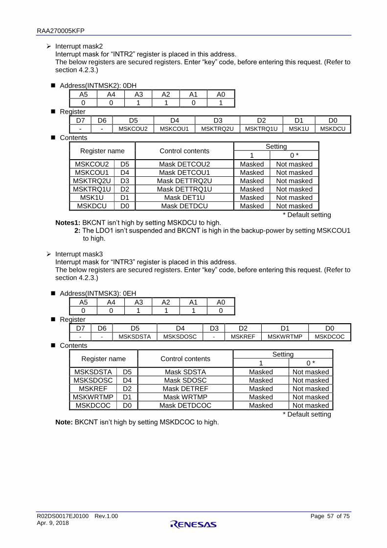
RAA270005KFP
R02DS0017EJ0100 Rev.1.00 Page 57 of 75 Apr. 9, 2018
Interrupt mask2 Interrupt mask for “INTR2” register is placed in this address. The below registers are secured registers. Enter “key” code, before entering this request. (Refer to section 4.2.3.) Address(INTMSK2): 0DH
A5 A4 A3 A2 A1 A0
0 0 1 1 0 1
Register
D7 D6 D5 D4 D3 D2 D1 D0
- - MSKCOU2 MSKCOU1 MSKTRQ2U MSKTRQ1U MSK1U MSKDCU
Contents
Register name Control contents Setting
1 0 *
MSKCOU2 D5 Mask DETCOU2 Masked Not masked
MSKCOU1 D4 Mask DETCOU1 Masked Not masked
MSKTRQ2U D3 Mask DETTRQ2U Masked Not masked
MSKTRQ1U D2 Mask DETTRQ1U Masked Not masked
MSK1U D1 Mask DET1U Masked Not masked
MSKDCU D0 Mask DETDCU Masked Not masked
* Default setting Notes1: BKCNT isn’t high by setting MSKDCU to high.
2: The LDO1 isn’t suspended and BKCNT is high in the backup-power by setting MSKCOU1 to high.
Interrupt mask3
Interrupt mask for “INTR3” register is placed in this address. The below registers are secured registers. Enter “key” code, before entering this request. (Refer to section 4.2.3.) Address(INTMSK3): 0EH
A5 A4 A3 A2 A1 A0
0 0 1 1 1 0
Register
D7 D6 D5 D4 D3 D2 D1 D0 - - MSKSDSTA MSKSDOSC - MSKREF MSKWRTMP MSKDCOC
Contents
Register name Control contents Setting
1 0 *
MSKSDSTA D5 Mask SDSTA Masked Not masked
MSKSDOSC D4 Mask SDOSC Masked Not masked
MSKREF D2 Mask DETREF Masked Not masked
MSKWRTMP D1 Mask WRTMP Masked Not masked
MSKDCOC D0 Mask DETDCOC Masked Not masked
* Default setting Note: BKCNT isn’t high by setting MSKDCOC to high.

RAA270005KFP
R02DS0017EJ0100 Rev.1.00 Page 58 of 75 Apr. 9, 2018
Interrupt mask4 Interrupt mask for “INTR4” register is placed in this address. The below registers are secured registers. Enter “key” code, before entering this request. (Refer to section 4.2.3.) Address(INTMSK4): 0FH
A5 A4 A3 A2 A1 A0
0 0 1 1 1 1
Register
D7 D6 D5 D4 D3 D2 D1 D0 - - - MSKPEXCNT2 MSKPEXCNT1 MSKPSUSP MSKPBKCNT MSKPRSTB
Contents
Register name Control contents Setting
1 0 *
MSKPEXCNT2 D4 Mask PEXCNT2 Masked Not masked
MSKPEXCNT1 D3 Mask PEXCNT1 Masked Not masked
MSKPSUSP D2 Mask PSUSP Masked Not masked
MSKPBKCNT D1 Mask PBKCNT Masked Not masked
MSKPRSTB D0 Mask PRSTB Masked Not masked
* Default setting

RAA270005KFP
R02DS0017EJ0100 Rev.1.00 Page 59 of 75 Apr. 9, 2018
The PMIC has a sort of protect function for a functional safety to protect MCU or the PMIC from extraordinary accident.
4.12.1. Voltage detection The buck DCDC, LDOs and trackers have voltage detectors. And a battery voltage detector has same function as well. High and low voltage detection1
Over and low voltage detection behaviors are shown in Figure 4-50. When over or low voltage is detected, INTOUT is asserted low.
Figure 4-50 Over and low voltage detector’s behavior
High and low voltage2
In the core voltage monitoring, the over (Vdcou2) and low (Vdcol1/2) voltage detection policy are different from the above behavior. The detectors have no release level and have anti glitch circuit to prevent nuisance reset.
Figure 4-51 Over and low voltage detector’s behavior for core voltage
LDO1/Buck DCDC /Tracker output
Detector output (Low voltage)
Detection voltage
Release voltage
Detection voltage
Detector output (High voltage)
Core voltage
Detection voltage
Detector output (Low voltage)
Detection voltage
Detector output (High voltage)
90μs 90μs

RAA270005KFP
R02DS0017EJ0100 Rev.1.00 Page 60 of 75 Apr. 9, 2018
4.12.2. PMIC behavior after unusual detection The PMIC have some over or low voltage, over current detectors and temperatures sensors. The behaviors in case of unusual detections are summarized below table.
Table 4-6 PMIC behavoir list in unusal conditons
Unusual detection Description Behavior of the PMIC
DETBAT Low voltage detection of battery Output reset signal
DETDCU Over voltage detection of buck DCDC
Stop Buck DCDC switching INTOUT: Low BKCNT: High*
DETDCL Low voltage detection of buck DCDC
Enter interval operating of buck DCDC INTOUT: Low BKCNT: High*
DETDCOC Over current detection of buck DCDC
Enter interval operating of buck DCDC INTOUT: Low BKCNT: High*
DETBSOC Over current detection of boost DCDC
INTOUT: Low
DET1U Over voltage detection of LDO1 INTOUT: Low
DET1L1 Low voltage detection of LDO1 SUSP, INTOUT, EXCNT1: Low EXCNT2: High BKCNT: High*
DET1L2 Low voltage detection of LDO1 Enter P/D sequence after reset
DETCOU1 Over absolute maximum detection of core voltage
Suspend LDO1
DETCOU2 Over voltage detection of core voltage
INTOUT: Low
LVCORE Low voltage detection of core voltage
Output reset, INTOUT: Low
DETCOL Low voltage detection of core voltage
Suspend LDO1 Enter P/D sequence after reset INTOUT: Low, Refer to Figure 4-52
DETTRQ1U Over voltage detection of TRACK1
INTOUT: Low
DETTRQ1L Low voltage detection of TRACK1
INTOUT: Low Stop TRACK1
DETTRQ2U Over voltage detection of TRACK2
INTOUT: Low
DETTRQ2L Low voltage detection of TRACK2
INTOUT: Low Stop TRACK2
DETTRQ1OC Over current detection of TRACK1
INTOUT: Low Stop TRACK1
DETTRQ2OC Over current detection of TRACK2
INTOUT: Low Stop TRACK2
WRTMP Warning temperature detection INTOUT: Low
TSDTMP Shut down temperature detection
INTOUT: Low Enter P/D sequence after reset
* If the backup power is detected
Figure 4-52 Low voltage detection behavior for core voltage at power up
Core voltage
INTOUT
RSTB 14.5ms
No power up core voltage

RAA270005KFP
R02DS0017EJ0100 Rev.1.00 Page 61 of 75 Apr. 9, 2018
4.12.3. Self-diagnosis Built-in-self-test is implemented in the PMIC so that self-diagnostic of the PMIC’s function is executed during initializing. The self-diagnostic is done to prevent serious situation such as applying unexpected voltage to MCU or communication disability with MCU. The following blocks are checked as self-diagnostic.
Detectors: Confirm the over/low detection function of regulators Logic circuit: Confirm logic function Oscillator: Confirm if the oscillation frequency is expected Temperature sensor: Confirm the function of thermal shutdown Backup-power: Confirm with or without the backup voltage and output voltage
Detectors
To make sure output voltage of each regulator, the detect functionality is tested before regulators power up. A voltage for comparator test is applied to the detector part. During diagnosis execution, detect function is checked by changing comparator’s input. If any error is detected, INTOUT is asserted.
Logic circuit The logic circuit in the PMIC is checked before reset is released. The self-diagnosis is done by test circuit implemented in the PMIC. If any error is detected in self-diagnosis, the PMIC does not start to operate.
Oscillator The oscillator is used for not only switching in DCDC but also state machine. Any damage in the oscillator may affect PMIC function. There are two oscillators which have quite same operation. They monitor oscillation each other, and if any unusual oscillation is detected then switched to the oscillator which acts usual operation. And then the PMIC set SDOSC to 1 and informs INTOUT assertion.
Temperature sensor The temperature sensor senses a voltage corresponding to the die temperature. During self-diagnosis period, the thermal shutdown function is checked. If any error is detected, INTOUT is asserted.
Backup-power The PMIC start up the backup-power by setting BKCNT is high once. The PMIC recognizes the backup-power if VOUT1 voltage is over DET1L. The PMIC starts the power up sequence after confirmation of the backup-power. SDBKUP set 1 if VOUT1 voltage is over Vr1l when BKCNT before LDO1 activation is low.

RAA270005KFP
R02DS0017EJ0100 Rev.1.00 Page 62 of 75 Apr. 9, 2018
4.12.4. Electrical characteristics The detection levels in each regulator are shown in below tables. Battery voltage detector
Table 4-7 Detection level of battery
Parameter Symbol Conditions MIN TYP MAX Unit
DETBAT
Detection voltage Vdbu VINR 3.50 3.65 3.80 V
Release voltage Vrbu VINR 5.00 5.25 5.50 V
DETBATBK
Detection voltage Vrbku VINR 7.40 7.70 8.00 V
Detector in buck DCDC
Table 4-8 Detection level of buck DCDC
Parameter Symbol Conditions MIN TYP MAX Unit
DETDCU
Detection voltage Vddu 6.90 7.15 7.40 V
Release voltage Vrdu 6.60 6.85 7.10 V
DETDCL
Detection voltage Vddl 2.70 2.85 3.00 V
Release voltage Vrdl 4.40 4.60 4.80 V
DETDCOC
Detection current Iddcoc* 750 - - mA
*: Guaranteed by Design Engineering Detector in boost DCDC
Table 4-9 Detection level of boost DCDC
Parameter Symbol Conditions MIN TYP MAX Unit
DETBSOC
Detection current Idbsoc* Current of 47mΩ(±5%) 2.2 - 2.7 A
*: Guaranteed by Design Engineering Detector in LDO0
Table 4-10 Detection level of LDO0
Parameter Symbol Conditions MIN TYP MAX Unit
DET0U
Detection voltage Vd0u 3.70 3.85 4.00 V
DET0L
Detection voltage Vd0l 3.000 3.081 3.164 V

RAA270005KFP
R02DS0017EJ0100 Rev.1.00 Page 63 of 75 Apr. 9, 2018
Detector in LDO1
Table 4-11 Detection level of LDO1
Parameter Symbol Conditions MIN TYP MAX Unit
DET1U
Detection voltage Vd1u 5.200 5.350 5.500 V
Release voltage Vr1u 5.100 5.250 5.400 V
DET1L1
Detection voltage Vd1l1 4.500 4.625 4.750 V
Release voltage Vr1l 4.650 4.775 4.900 V
DET1L2
Detection voltage Vd1l2 3.020 3.110 3.200 V
Note: RSTB is low if DET1L2 is detected. Detector in TRACK1
Table 4-12 Detection level of TRAK1
Parameter Symbol Conditions MIN TYP MAX Unit
DETTRQ1U
Detection voltage Vdtr1u Based on VOUT1 104.0 107.0 110.0 %
Release voltage Vrtr1u Based on VOUT1 102.0 105.0 108.0 %
DETTRQ1L
Detection voltage Vdtr1l TRQLVSEL=0, Based on VOUT1 47.0 48.6 50.2 % TRQLVSEL=1, Based on VOUT1 90.0 92.5 95.0 %
Detection voltage Vrtr1l Based on VOUT1 93.0 95.5 98.0 %
DETTRQ1OC
Detection current Idtr1oc 230 - 700 mA
Detector in TRACK2
Table 4-13 Detection level of TRACK2
Parameter Symbol Conditions MIN TYP MAX Unit
DETTRQ2U
Detection voltage Vdtr2u Based on VOUT1 104.0 107.0 110.0 %
Release voltage Vrtr2u Based on VOUT1 102.0 105.0 108.0 %
DETTRQ2L
Detection voltage Vdtr2l TRQLVSEL=0, Based on VOUT1 47.0 48.6 50.2 % TRQLVSEL=1, Based on VOUT1 90.0 92.5 95.0 %
Detection voltage Vrtr2l Based on VOUT1 93.0 95.5 98.0 %
DETTRQ2OC
Detection current Idtr2oc 230 - 700 mA

RAA270005KFP
R02DS0017EJ0100 Rev.1.00 Page 64 of 75 Apr. 9, 2018
Detector in core voltage
Table 4-14 Detection level of core voltage
Parameter Symbol Conditions MIN TYP MAX Unit
DETCOU1
Detection voltage Vdcou1 1.50 1.55 1.60 V
Release voltage Vrcou1 1.42 1.48 1.53 V
DETCOU2
Detection voltage Vdcou2 1.35 1.38 1.40 V
LVCORE
Detection voltage Vdcol1 1.10 1.13 1.15 V
DETCOL
Detection voltage Vdcol2 0.90 0.95 1.00 V
Notes1: RSTB is low if LVCORE is detected 2: The PMIC enters the power down sequence if DETCOL is detected

RAA270005KFP
R02DS0017EJ0100 Rev.1.00 Page 65 of 75 Apr. 9, 2018
Temperature sensors are implemented in the PMIC.
4.13.1. Thermal shutdown For product safety, thermal shutdown functions are implemented. Temperature sensors detect a voltage corresponding to the internal temperature. When warning temperature is detected, INTOUT asserts low. The temperature sensors are placed near by buck DCDC, and LDO1. If one of these sensors detects high junction temperature, INTOUT asserts low and the reset signal is released and the PMIC execute power down sequence. After the junction temperature goes down across the release temperature, the PMIC restarts in the power-up sequence. Resuming TRACK1 and TRACK2 operation requires that VTPQ1CNT and VTRQ2CNT are 1 due to initialize these registers.
Table 4-15 Thermal detection
Parameter Symbol Conditions MIN TYP MAX Unit
Warning temperature Twng 140 160 180
°C
Shutdown temperature Tsd 160 180 200
Released temperature Trls 125 145 165
Warning released temperature
Twrls 115 135 155
Note: Above values are guaranteed by Design Engineering. Relationship of above temperature order maintains any time.
Figure 4-53 Thermal shutdown function
4.13.2. Register The temperature setting of both detect and release can be changed. The shutdown temperature is fixed at 180°C (TYP) Temperature setting
The below registers are secured registers. Enter “key” code, before entering this request. (Refer to section 4.2.3.) Address (SENTMP): 1EH
A5 A4 A3 A2 A1 A0
0 1 1 1 1 0
Register
D7 D6 D5 D4 D3 D2 D1 D0
WARREL (1:0) THREL (1:0) WARDET (1:0) - -
Temperature
Time
Shutdown Temp. Warning Temp.
Released Temp.
Warning released Temp.
Regulators
Power up sequence
Interrupt
Power down sequence
Interrupt conditions

RAA270005KFP
R02DS0017EJ0100 Rev.1.00 Page 66 of 75 Apr. 9, 2018
Setting contents
WARDET (1:0) Warning temp.
THREL (1:0) Shutdown release
D3 D2 D5 D4
0 0 170°C 0 0 155°C
0 1 160°C * 0 1 145°C *
1 0 150°C 1 0 135°C
1 1 140°C 1 1 125°C
* Default setting * Default setting
WARREL (1:0) Warning release
D7 D6
0 0 155°C
0 1 145°C
1 0 135°C *
1 1 125°C
* Default setting

RAA270005KFP
R02DS0017EJ0100 Rev.1.00 Page 67 of 75 Apr. 9, 2018
The PMIC has monitoring functions. The analog monitoring function is indicated internal analog voltages. The digital monitoring function is monitoring digital output pins.
4.14.1. Internal analog voltage monitoring The PMIC has an analog monitoring function and outputs the regulator level of the PMIC or internal analog voltages with using operational amplifier. A MCU can read these analog voltages through its ADC. Setting register controls output and channel.
Figure 4-54 Diagram of analog monitoring
4.14.2. Digital output monitoring The PMIC has a digital monitoring function and compares with output and control signal of digital output buffer. If differentiation is detected, the PMIC makes INTOUT assert low. The objective outputs are EXCNT1/2, SUSP, RSTB and BKCNT pins. INTOUT pin isn’t monitored. For checking the operation of INTOUT, set the "DUMMY" bit of the interrupt. EXCNT1/2, SUSP and BKCNT monitoring are started after 2μs each changed, RSTB monitoring is started after 100μs.
Figure 4-55 Diagram of digital monitoring
MUXOUT
AMUXIN1
AMUXIN2
Multiplexer decoder
TEMP1 (Near buck DCDC)
TEMP2 (Near LDO1)
VDC (FBDC)
VOUT0
VOUT1
VTRQ1
VTRQ2
VINR
ENIG
VREF1
Digital output Output signal
Output buffer
Interrupt control Delay

RAA270005KFP
R02DS0017EJ0100 Rev.1.00 Page 68 of 75 Apr. 9, 2018
4.14.3. Register The operation setting for monitoring function is described in this section. Signal select Address (MUXCNT): 18H
A5 A4 A3 A2 A1 A0
0 1 1 0 0 0
Register
D7 D6 D5 D4 D3 D2 D1 D0
- MUXCNT - - MUXSEL (3:0)
Setting contents This bit controls on/off control for the analog monitoring
Register name Control content Setting
1 0
MUXCNT D6 On/Off control On Off *
* Default setting These bits control the output channel. The analog monitoring outputs 0V in the GND level. And when the analog monitoring selects AMUXIN1/2 and over VOUT1 is input to AMUXIN1/2, MUXOUT outputs VOUT1-0.2V.
MUXSEL (3:0) Monitoring name
D3 D2 D1 D0
0 0 0 0 GND level*
0 0 0 1 VINR
0 0 1 0 ENIG
0 0 1 1 FBDC
0 1 0 0 VOUT0
0 1 0 1 VOUT1
0 1 1 0 VTRQ1
0 1 1 1 VTRQ2
1 0 0 0 VREF1
1 0 0 1 TEMP1 (Near Buck DCDC)
1 0 1 0 TEMP2 (Near LDO1)
1 0 1 1 AMUXIN1
1 1 0 0 AMUXIN2
1 1 0 1 GND level
1 1 1 0 GND level
1 1 1 1 GND level
* Default setting
4.14.4. Electrical characteristics Input current
Parameter Symbol Conditions MIN TYP MAX Unit
Input current Ilmux1/2 AMUXIN1/2 - - 2.0 μA

RAA270005KFP
R02DS0017EJ0100 Rev.1.00 Page 69 of 75 Apr. 9, 2018
Output voltage (4.9V ≤ VOUT1 ≤ 5.1V)
Parameter Symbol Conditions MIN TYP MAX Unit
Output voltage
Xinr Selected VINR (6.6V ≤ VINR ≤ 28.0V)
0.097 0.10 0.103 Times
XENIG
Selected ENIG (6.6V ≤ ENIG ≤ 28.0V)
0.097 0.10 0.103
Selected ENIG (0V ≤ ENIG ≤ 6.6V), VOUT1 ≥ 4.9V
ENIG/10 -0.02
ENIG/10 ENIG/10
+0.02
V
Xdc Selected FBDC (VoDC)/2
-0.12 (VoDC)/2
(VoDC)/2 +0.12
Xldo0 Selected VOUT0 (VOUT0)/2
-0.17 (VOUT0)/2
(VOUT0)/2 +0.17
Xldo1 Selected VOUT1 (VOUT1)/2
-0.04 (VOUT1)/2
(VOUT1)/2 +0.04
Xtraq1 Selected VTRQ1 (VOUT1)/2
-0.05 (VOUT1)/2
(VOUT1)/2 +0.05
Xtraq2 Selected VTRQ2 (VOUT1)/2
-0.04 (VOUT1)/2
(VOUT1)/2 +0.04
Vref Selected VREF1 1.159 1.20 1.241
Votmp1 Selected temperature sensor @25°C (Near buck DCDC)
3.12 3.38 3.65
Votmp2 Selected temperature sensor @25°C (Near LDO1)
3.12 3.38 3.65
Input voltage range
Xin1 Selected AMUXIN1 |MUXOUT-AMUXIN1| ≤ 10mV
0.2 2.5 VOUT1
-0.2
Xin2 Selected AMUXIN2 |MUXOUT-AMUXIN2| ≤ 10mV
0.2 2.5 VOUT1
-0.2
Output stable time
Tstb * From SPICSB rising, Co=50pF
- - 40 μs
*: Guaranteed by Design Engineering
Figure 4-56 Output timing
SPICLK
SPICSB
tstb
MUXOUT

RAA270005KFP
R02DS0017EJ0100 Rev.1.00 Page 70 of 75 Apr. 9, 2018
Output of temperature sensor The outputs of temperature depend on the junction temperature. For reference, the output temperature characteristic is shown in below figure. The approximate equation of the output voltage is as follow. And output deviation is ±315mV for every temperature. Votmp1/2=3.618-0.01*T (V) “T”: Junction temperature
Figure 4-57 Output of temperature sensor
Junction Temperature (°C)
Outp
ut V
oltage (
V)

RAA270005KFP
R02DS0017EJ0100 Rev.1.00 Page 71 of 75 Apr. 9, 2018
5. Application Example Below figures show typical application diagrams which contain elements around the PMIC.
D M1FS4 (SHINDENGEN) L CLF6045T-4R7M or CLF6045NIT-4R7N (TDK) C1, C2 GCM21BR71H105K (MURATA) C3 GCM31CR71C475K (MURATA) C4 GCM21BR701J106K (MURATA) C5, C6 GCM21BR71C225K (MURATA) C7 GCM188R71C104K (MURATA) C8 GCM219R71C105K (MURATA)
Figure 5-1 Applicaiton ciruit example1 (Boost DCDC non-use)
Note: This is a very simplified example of an application. The function must be verified in the real
application.
EVCC
AVCC
VCL
VCC
ADCA
Battery (12V)
CSIHnCSSn CSIHnSCO
CSIHnSO
CSIHnSI GPIOn INTn ERROROUT INTn RESET GPIOn
D
L 4.7uH
C1 1μF
C2 1μF
C3 4.7μF x2pcs
C4 10μF
C8 1μF
C5 2.2μF
C6 2.2μF
C7 0.1μF
OUT CNT
Backup-power
RH850/P1x
RAA270005KFP
VINR VIN3V VOUT0
ENIG
EN
SPICSB SPICLK
SPISDI
SPISDO
WDI
INTOUT
ERROR
SUSP
RSTB
MUXOUT
VINPDC
FBDC LX
VINP1 VOUT1
BUFREF
AGND1~3
TEST1/2
VINPTRQ
VTRQ1
VTRQ2
VDDIO
COREMON
BKCNT
AMUXIN1/2
EXCNT1/2
To control other devices
VINPBS
BSGATE
CSR
CSGND

RAA270005KFP
R02DS0017EJ0100 Rev.1.00 Page 72 of 75 Apr. 9, 2018
D1 M1FS4 (SHINDENGEN) D2 M1FM3 (SHINDENGEN) or RB068MM-40(ROHM) L1 CLF6045T-4R7N (TDK) L2 CLF7045T-100M (TDK) C1, C2, C9 GCM21BR71H105K (MURATA) C3 GCM31CR71C475K (MURATA) C4 GCM21BR701J106K (MURATA) C5, C6 GCM21BR71C225K (MURATA) C7 GCM188R71C104K (MURATA) C8 EMVY500ADA470MF80G (NIPPON CHEMI-CON) C10 GCM219R71C105K (MURATA)
TR RTR030N05 (ROHM)
Figure 5-2 Application circuit example2 (Boost DCDC use)
Note: This is a very simplified example of an application. The function must be verified in the real
application.
EVCC
AVCC
VCL
VCC
ADCA
Battery (12V)
To control other devices
D1
L1 4.7uH
C1 1μF
C2 1μF
C3 4.7μFX2pcs
C4 10μF
C10 1μF
C5 2.2μF
C6 2.2μF
C7 0.1μF
OUT CNT
Backup-power
RH850/P1x
RAA270005KFP
VINR VIN3V VOUT0
ENIG
EN
SPICSB SPICLK
SPISDI
SPISDO
WDI
INTOUT
ERROR
SUSP
RSTB
MUXOUT
VINPDC
FBDC LX
VINP1 VOUT1
BUFREF
AGND1~3
TEST1/2
VINPTRQ
VTRQ1
VTRQ2
VDDIO
COREMON
BKCNT
AMUXIN1/2
EXCNT1/2
VINPBS
BSGATE
CSR
CSGND
C8 47μF
L2 10uH D2
TR
R1 47mΩ
C9 1μF
CSIHnCSSn CSIHnSCO
CSIHnSO
CSIHnSI GPIOn INTn ERROROUT INTn RESET GPIOn
R2 1Ω

RAA270005KFP
R02DS0017EJ0100 Rev.1.00 Page 73 of 75 Apr. 9, 2018
Important thing to consider the layout is component placement on the PCB. Take care following things for PCB trace design. For proper operation and to prevent EMI radiation, the freewheeling diode and inductor have to be
placed as close as possible to the PMIC. Also, the output capacitors have to be placed near by the inductor.
The feedback trace of buck DCDC converter never crosses the inductor, and recommended connection point is near output capacitor
For buck DCDC converter, GND connection of components is important. GNDs of input capacitor, output capacitor, and freewheeling diode are connected to the same point.
For LDO, in order to avoid influence of stray resistance on the PCB, output capacitor has to be placed as close as possible to the PMIC.
If application needs to apply power supply for multi devices, power distribution at output capacitor of each regulator is recommended.
In order to maximum heat spread performance, the exposed pad on the backside of the package is recommended to make soldering to GND plane.

RAA270005KFP
R02DS0017EJ0100 Rev.1.00 Page 74 of 75 Apr. 9, 2018
6. Electrical Characteristics
Parameter Symbol Pin name MIN TYP MAX Unit
Input voltage VBAT VINR, VINPDC 6.6 12.0 18.5 V
LDO power line VPLDO VINP1, VINPTRQ 5.8 6.1 6.4 V
Digital I/O power VDDIO VDDIO, VINPBS 3.0 5.0 5.5 V
Circuit power line VIN3V VIN3V 3.0 3.3 3.6 V
6.2.1. DC characteristics Digital input
DC characteristics of digital input pins are shown in the below table.
Parameter Symbol Pin name MIN TYP MAX Unit
High level input voltage 1 VIH1 ENIG 2.5 - - V
High level input voltage 2 VIH2 Below pin group VDDIO*0.7 - - V
Low level input voltage 1 VIL1 ENIG - - 1.0 V
Low level input voltage 2 VIL2 Below pin group - - VDDIO*0.3 V
Pin group: EN, SPICSB, SPICLK, SPISDI, WDI and ERROR Digital output
DC characteristics of digital output pins are shown in the below table.
Parameter Symbol Pin name MIN TYP MAX Unit
High level output voltage 1 VOH1 Below pin group, IoH=2mA
VDDIO*0.8 - -
V
High level output voltage 2 VOH2 BKCNT, IoH=1mA VIN3V*0.8 - - V
High level output voltage 3 VOH3 SPISDO, IoH=5mA VDDIO*0.8 - - V
Low level output voltage 1 VOL1 Below pin group, IoL=-2mA
- - VDDIO*0.2 V
Low level output voltage 2 VOL2 BKCNT, IoL=-1mA - - VIN3V*0.2 V
Low level output voltage 3 VOL3 SPISDO, IoL=-5mA - - VDDIO*0.2 V
Low level output voltage 4 VOL4 RSTB, IoL=-0.1mA - - 0.4 V
Pin group: INTOUT, SUSP and EXCNT1/2 Pull up/down resistance
Parameter Symbol Condition MIN TYP MAX Unit
Pull up resistor 1 Rpu SPICSB 76 100 127 kΩ
Pull up resistor 2 Rpurs RSTB 2.6 3.3 4.2 kΩ
Pull down resistor 1 RpdIG ENIG 390 - - kΩ
Pull down resistor 2 Rpd Below pin group 76 100 127 kΩ
Pin group: EN, SPICLK, SPISDI, WDI and ERROR Operating current (Non-load current on each regulator)
Parameter Symbol Condition MIN TYP MAX Unit
Stand-by current Ioff ENIG=0, EN=0, -40 ≤ Tj ≤ 85°C
- 5.0 10 μA
Operating current 1 Idd1* ENIG=1 or EN=1 - 2.4 4.5 mA
Operating current 2 Idd2* Idd1 + Tracker + Analog monitor
- 5.4 14 mA
Operating current 3 Idd3* Idd2 + Boost DCDC - - 15 mA
* Except the external diode leakage current

RAA270005KFP
R02DS0017EJ0100 Rev.1.00 Page 75 of 75 Apr. 9, 2018
7. Package Information
Figure 7-1 Package

All trademarks and registered trademarks are the property of their respective owners.
C-1
Revision History RAA270005KFP Data Sheet
Rev. Date
Description
Page Summary
1.00 Apr. 2018 - Initial

http://www.renesas.comRefer to "http://www.renesas.com/" for the latest and detailed information.
Renesas Electronics America Inc.1001 Murphy Ranch Road, Milpitas, CA 95035, U.S.A.Tel: +1-408-432-8888, Fax: +1-408-434-5351Renesas Electronics Canada Limited9251 Yonge Street, Suite 8309 Richmond Hill, Ontario Canada L4C 9T3Tel: +1-905-237-2004Renesas Electronics Europe LimitedDukes Meadow, Millboard Road, Bourne End, Buckinghamshire, SL8 5FH, U.KTel: +44-1628-651-700, Fax: +44-1628-651-804Renesas Electronics Europe GmbHArcadiastrasse 10, 40472 Düsseldorf, Germany Tel: +49-211-6503-0, Fax: +49-211-6503-1327Renesas Electronics (China) Co., Ltd.Room 1709 Quantum Plaza, No.27 ZhichunLu, Haidian District, Beijing, 100191 P. R. ChinaTel: +86-10-8235-1155, Fax: +86-10-8235-7679Renesas Electronics (Shanghai) Co., Ltd.Unit 301, Tower A, Central Towers, 555 Langao Road, Putuo District, Shanghai, 200333 P. R. China Tel: +86-21-2226-0888, Fax: +86-21-2226-0999Renesas Electronics Hong Kong LimitedUnit 1601-1611, 16/F., Tower 2, Grand Century Place, 193 Prince Edward Road West, Mongkok, Kowloon, Hong KongTel: +852-2265-6688, Fax: +852 2886-9022Renesas Electronics Taiwan Co., Ltd.13F, No. 363, Fu Shing North Road, Taipei 10543, TaiwanTel: +886-2-8175-9600, Fax: +886 2-8175-9670Renesas Electronics Singapore Pte. Ltd.80 Bendemeer Road, Unit #06-02 Hyflux Innovation Centre, Singapore 339949Tel: +65-6213-0200, Fax: +65-6213-0300Renesas Electronics Malaysia Sdn.Bhd.Unit 1207, Block B, Menara Amcorp, Amcorp Trade Centre, No. 18, Jln Persiaran Barat, 46050 Petaling Jaya, Selangor Darul Ehsan, MalaysiaTel: +60-3-7955-9390, Fax: +60-3-7955-9510Renesas Electronics India Pvt. Ltd.No.777C, 100 Feet Road, HAL 2nd Stage, Indiranagar, Bangalore 560 038, IndiaTel: +91-80-67208700, Fax: +91-80-67208777Renesas Electronics Korea Co., Ltd.17F, KAMCO Yangjae Tower, 262, Gangnam-daero, Gangnam-gu, Seoul, 06265 KoreaTel: +82-2-558-3737, Fax: +82-2-558-5338
SALES OFFICES
© 2018 Renesas Electronics Corporation. All rights reserved.Colophon 7.0
(Rev.4.0-1 November 2017)
Notice
1. Descriptions of circuits, software and other related information in this document are provided only to illustrate the operation of semiconductor products and application examples. You are fully responsible for
the incorporation or any other use of the circuits, software, and information in the design of your product or system. Renesas Electronics disclaims any and all liability for any losses and damages incurred by
you or third parties arising from the use of these circuits, software, or information.
2. Renesas Electronics hereby expressly disclaims any warranties against and liability for infringement or any other claims involving patents, copyrights, or other intellectual property rights of third parties, by or
arising from the use of Renesas Electronics products or technical information described in this document, including but not limited to, the product data, drawings, charts, programs, algorithms, and application
examples.
3. No license, express, implied or otherwise, is granted hereby under any patents, copyrights or other intellectual property rights of Renesas Electronics or others.
4. You shall not alter, modify, copy, or reverse engineer any Renesas Electronics product, whether in whole or in part. Renesas Electronics disclaims any and all liability for any losses or damages incurred by
you or third parties arising from such alteration, modification, copying or reverse engineering.
5. Renesas Electronics products are classified according to the following two quality grades: “Standard” and “High Quality”. The intended applications for each Renesas Electronics product depends on the
product’s quality grade, as indicated below.
"Standard": Computers; office equipment; communications equipment; test and measurement equipment; audio and visual equipment; home electronic appliances; machine tools; personal electronic
equipment; industrial robots; etc.
"High Quality": Transportation equipment (automobiles, trains, ships, etc.); traffic control (traffic lights); large-scale communication equipment; key financial terminal systems; safety control equipment; etc.
Unless expressly designated as a high reliability product or a product for harsh environments in a Renesas Electronics data sheet or other Renesas Electronics document, Renesas Electronics products are
not intended or authorized for use in products or systems that may pose a direct threat to human life or bodily injury (artificial life support devices or systems; surgical implantations; etc.), or may cause
serious property damage (space system; undersea repeaters; nuclear power control systems; aircraft control systems; key plant systems; military equipment; etc.). Renesas Electronics disclaims any and all
liability for any damages or losses incurred by you or any third parties arising from the use of any Renesas Electronics product that is inconsistent with any Renesas Electronics data sheet, user’s manual or
other Renesas Electronics document.
6. When using Renesas Electronics products, refer to the latest product information (data sheets, user’s manuals, application notes, “General Notes for Handling and Using Semiconductor Devices” in the
reliability handbook, etc.), and ensure that usage conditions are within the ranges specified by Renesas Electronics with respect to maximum ratings, operating power supply voltage range, heat dissipation
characteristics, installation, etc. Renesas Electronics disclaims any and all liability for any malfunctions, failure or accident arising out of the use of Renesas Electronics products outside of such specified
ranges.
7. Although Renesas Electronics endeavors to improve the quality and reliability of Renesas Electronics products, semiconductor products have specific characteristics, such as the occurrence of failure at a
certain rate and malfunctions under certain use conditions. Unless designated as a high reliability product or a product for harsh environments in a Renesas Electronics data sheet or other Renesas
Electronics document, Renesas Electronics products are not subject to radiation resistance design. You are responsible for implementing safety measures to guard against the possibility of bodily injury, injury
or damage caused by fire, and/or danger to the public in the event of a failure or malfunction of Renesas Electronics products, such as safety design for hardware and software, including but not limited to
redundancy, fire control and malfunction prevention, appropriate treatment for aging degradation or any other appropriate measures. Because the evaluation of microcomputer software alone is very difficult
and impractical, you are responsible for evaluating the safety of the final products or systems manufactured by you.
8. Please contact a Renesas Electronics sales office for details as to environmental matters such as the environmental compatibility of each Renesas Electronics product. You are responsible for carefully and
sufficiently investigating applicable laws and regulations that regulate the inclusion or use of controlled substances, including without limitation, the EU RoHS Directive, and using Renesas Electronics
products in compliance with all these applicable laws and regulations. Renesas Electronics disclaims any and all liability for damages or losses occurring as a result of your noncompliance with applicable
laws and regulations.
9. Renesas Electronics products and technologies shall not be used for or incorporated into any products or systems whose manufacture, use, or sale is prohibited under any applicable domestic or foreign laws
or regulations. You shall comply with any applicable export control laws and regulations promulgated and administered by the governments of any countries asserting jurisdiction over the parties or
transactions.
10. It is the responsibility of the buyer or distributor of Renesas Electronics products, or any other party who distributes, disposes of, or otherwise sells or transfers the product to a third party, to notify such third
party in advance of the contents and conditions set forth in this document.
11. This document shall not be reprinted, reproduced or duplicated in any form, in whole or in part, without prior written consent of Renesas Electronics.
12. Please contact a Renesas Electronics sales office if you have any questions regarding the information contained in this document or Renesas Electronics products.
(Note 1) “Renesas Electronics” as used in this document means Renesas Electronics Corporation and also includes its directly or indirectly controlled subsidiaries.
(Note 2) “Renesas Electronics product(s)” means any product developed or manufactured by or for Renesas Electronics.