Embed Size (px)
Citation preview

R01DS0010EJ0200 Rev.2.00 Page 1 of 45May 31, 2012
R8C/M11A Group, R8C/M12A GroupRENESAS MCU
Datasheet
1. Overview
1.1 FeaturesThe R8C/M11A Group and R8C/M12A Group of single-chip microcontrollers (MCUs) incorporate the R8C CPUcore, which provides sophisticated instructions for a high level of efficiency. With 1 Mbyte of address space, theCPU core is capable of executing instructions at high speed. In addition, it features a multiplier for high-speedarithmetic processing.Power consumption is low, and the supported operating modes allow additional power control. These MCUs aredesigned to maximize EMI/EMS performance.Integration of many peripheral functions on the same chip, including multifunction timer and serial interface,reduces the number of system components.The R8C/M11A Group and R8C/M12A Group include data flash (1 KB × 2 blocks).
1.1.1 ApplicationsHome appliances, office equipment, audio equipment, consumer products, etc.
R01DS0010EJ0200Rev.2.00
May 31, 2012

R8C/M11A Group, R8C/M12A Group 1. Overview
R01DS0010EJ0200 Rev.2.00 Page 2 of 45May 31, 2012
1.1.2 Differences between GroupsTable 1.1 lists the Specification Comparison between R8C/M11A Group and R8C/M12A Group. Theexplanations in 1.1.3 and subsequent sections apply to the R8C/M12A Group specifications only, unlessotherwise specified.
Table 1.1 Specification Comparison between R8C/M11A Group and R8C/M12A GroupItem Function R8C/M11A Group R8C/M12A Group
Interrupts External interrupt inputs 6 (INT × 3, key input × 3) 8 (INT × 4, key input × 4)I/O ports Number of pins 14
Non-provided pins: P1_0/AN0/TRCIOD/KI0P3_3/IVCMP3/TRCCLK/INT3P3_4/IVREF3/TRCIOC/INT2P3_5/TRCIOD/KI2/VCOUT3P4_2/TRBO/TXD0/KI3P4_5/INT0/ADTRG
20
Number of CMOS I/O ports 11Non-provided ports:
P1_0, P3_3, P3_4, P3_5, P4_2, P4_5
17
Number of high-current drive ports
5Non-provided ports:
P3_3, P3_4, P3_5
8
A/D converter Number of A/D channels 5 channelsNon-provided port: AN0
6 channels
Comparator B Number of channels Comparator B1 Comparator B1, comparator B3
R8C/M11A Group, R8C/M12A Group 1. Overview
R01DS0010EJ0200 Rev.2.00 Page 3 of 45May 31, 2012
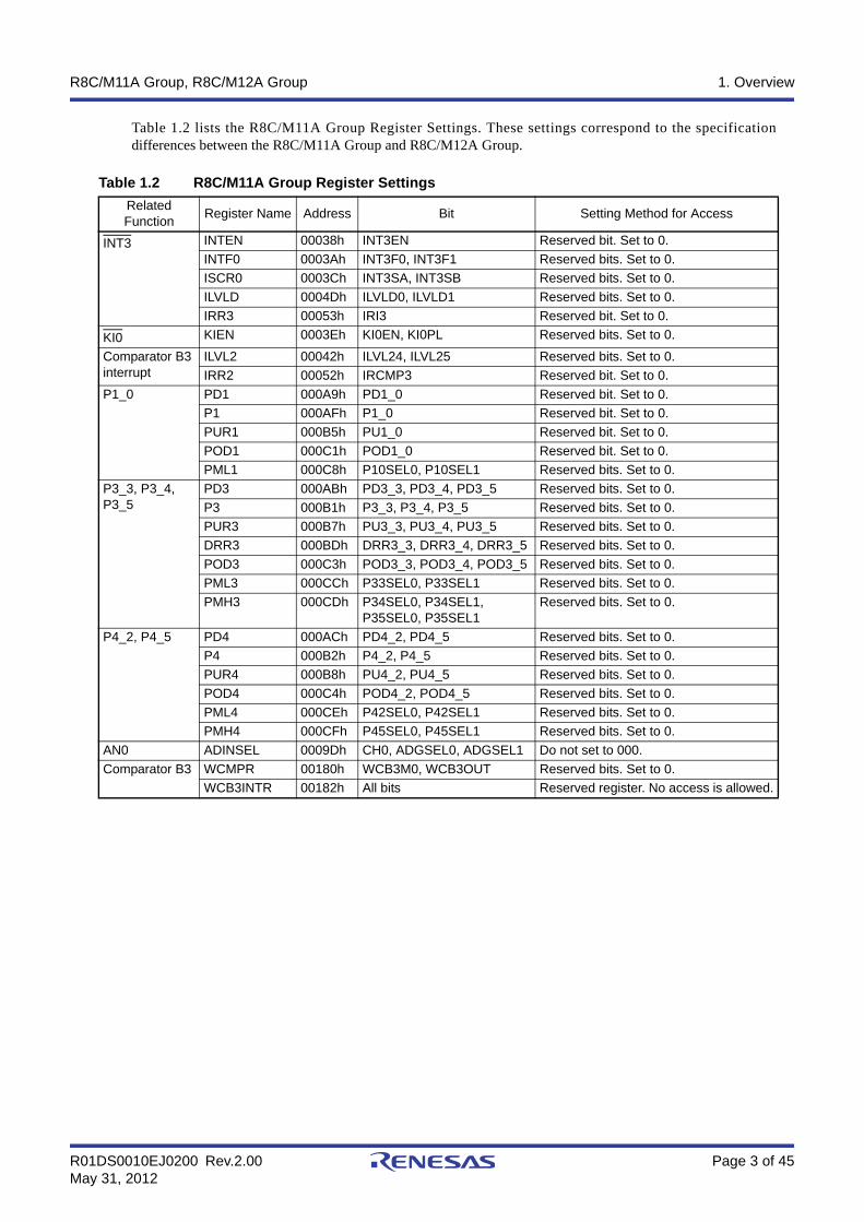
Table 1.2 lists the R8C/M11A Group Register Settings. These settings correspond to the specificationdifferences between the R8C/M11A Group and R8C/M12A Group.
Table 1.2 R8C/M11A Group Register SettingsRelated Function Register Name Address Bit Setting Method for Access
INT3 INTEN 00038h INT3EN Reserved bit. Set to 0.INTF0 0003Ah INT3F0, INT3F1 Reserved bits. Set to 0.ISCR0 0003Ch INT3SA, INT3SB Reserved bits. Set to 0.ILVLD 0004Dh ILVLD0, ILVLD1 Reserved bits. Set to 0.IRR3 00053h IRI3 Reserved bit. Set to 0.
KI0 KIEN 0003Eh KI0EN, KI0PL Reserved bits. Set to 0.
Comparator B3 interrupt
ILVL2 00042h ILVL24, ILVL25 Reserved bits. Set to 0.IRR2 00052h IRCMP3 Reserved bit. Set to 0.
P1_0 PD1 000A9h PD1_0 Reserved bit. Set to 0.P1 000AFh P1_0 Reserved bit. Set to 0.PUR1 000B5h PU1_0 Reserved bit. Set to 0.POD1 000C1h POD1_0 Reserved bit. Set to 0.PML1 000C8h P10SEL0, P10SEL1 Reserved bits. Set to 0.
P3_3, P3_4, P3_5
PD3 000ABh PD3_3, PD3_4, PD3_5 Reserved bits. Set to 0.P3 000B1h P3_3, P3_4, P3_5 Reserved bits. Set to 0.PUR3 000B7h PU3_3, PU3_4, PU3_5 Reserved bits. Set to 0.DRR3 000BDh DRR3_3, DRR3_4, DRR3_5 Reserved bits. Set to 0.POD3 000C3h POD3_3, POD3_4, POD3_5 Reserved bits. Set to 0.PML3 000CCh P33SEL0, P33SEL1 Reserved bits. Set to 0.PMH3 000CDh P34SEL0, P34SEL1,
P35SEL0, P35SEL1Reserved bits. Set to 0.
P4_2, P4_5 PD4 000ACh PD4_2, PD4_5 Reserved bits. Set to 0.P4 000B2h P4_2, P4_5 Reserved bits. Set to 0.PUR4 000B8h PU4_2, PU4_5 Reserved bits. Set to 0.POD4 000C4h POD4_2, POD4_5 Reserved bits. Set to 0.PML4 000CEh P42SEL0, P42SEL1 Reserved bits. Set to 0.PMH4 000CFh P45SEL0, P45SEL1 Reserved bits. Set to 0.
AN0 ADINSEL 0009Dh CH0, ADGSEL0, ADGSEL1 Do not set to 000.Comparator B3 WCMPR 00180h WCB3M0, WCB3OUT Reserved bits. Set to 0.
WCB3INTR 00182h All bits Reserved register. No access is allowed.
R8C/M11A Group, R8C/M12A Group 1. Overview
R01DS0010EJ0200 Rev.2.00 Page 4 of 45May 31, 2012
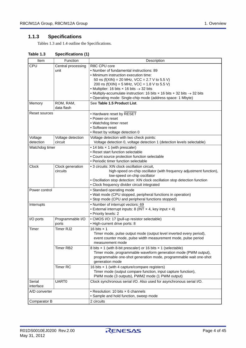
1.1.3 SpecificationsTables 1.3 and 1.4 outline the Specifications.
Table 1.3 Specifications (1)Item Function Description
CPU Central processing unit
R8C CPU core• Number of fundamental instructions: 89• Minimum instruction execution time:
50 ns (f(XIN) = 20 MHz, VCC = 2.7 V to 5.5 V)200 ns (f(XIN) = 5 MHz, VCC = 1.8 V to 5.5 V)
• Multiplier: 16 bits × 16 bits → 32 bits• Multiply-accumulate instruction: 16 bits × 16 bits + 32 bits → 32 bits• Operating mode: Single-chip mode (address space: 1 Mbyte)
Memory ROM, RAM, data flash
See Table 1.5 Product List.
Reset sources • Hardware reset by RESET• Power-on reset• Watchdog timer reset• Software reset• Reset by voltage detection 0
Voltage detection
Voltage detection circuit
Voltage detection with two check points:Voltage detection 0, voltage detection 1 (detection levels selectable)
Watchdog timer • 14 bits × 1 (with prescaler)• Reset start function selectable• Count source protection function selectable• Periodic timer function selectable
Clock Clock generation circuits
• 3 circuits: XIN clock oscillation circuit, high-speed on-chip oscillator (with frequency adjustment function), low-speed on-chip oscillator
• Oscillation stop detection: XIN clock oscillation stop detection function• Clock frequency divider circuit integrated
Power control • Standard operating mode• Wait mode (CPU stopped, peripheral functions in operation)• Stop mode (CPU and peripheral functions stopped)
Interrupts • Number of interrupt vectors: 69• External interrupt inputs: 8 (INT × 4, key input × 4)• Priority levels: 2
I/O ports Programmable I/O ports
• CMOS I/O: 17 (pull-up resistor selectable)• High-current drive ports: 8
Timer Timer RJ2 16 bits × 1Timer mode, pulse output mode (output level inverted every period), event counter mode, pulse width measurement mode, pulse period measurement mode
Timer RB2 8 bits × 1 (with 8-bit prescaler) or 16 bits × 1 (selectable)Timer mode, programmable waveform generation mode (PWM output), programmable one-shot generation mode, programmable wait one-shot generation mode
Timer RC 16 bits × 1 (with 4 capture/compare registers)Timer mode (output compare function, input capture function), PWM mode (3 outputs), PWM2 mode (1 PWM output)
Serial interface
UART0 Clock synchronous serial I/O. Also used for asynchronous serial I/O.
A/D converter • Resolution: 10 bits × 6 channels• Sample and hold function, sweep mode
Comparator B 2 circuits

R8C/M11A Group, R8C/M12A Group 1. Overview
R01DS0010EJ0200 Rev.2.00 Page 5 of 45May 31, 2012
Note:1. Specify the D version if it is to be used.
Table 1.4 Specifications (2)Item Function Description
Flash memory • Program/erase voltage for program ROM: VCC = 1.8 V to 5.5 V• Program/erase voltage for data flash: VCC = 1.8 V to 5.5 V• Program/erase endurance:10,000 times (data flash)
10,000 times (program ROM)• Program security: ID code check, protection enabled by lock bit• Debug functions: On-chip debug, on-board flash rewrite function
Operating frequency/Power supply voltage
f(XIN) = 20 MHz (VCC = 2.7 V to 5.5 V)f(XIN) = 5 MHz (VCC = 1.8 V to 5.5 V)
Temperature range -20 °C to 85 °C (N version)-40 °C to 85 °C (D version) (1)
Package 14-pin TSSOP: [Package code] PTSP0014JA-B14-pin DIP: [Package code] PRDP0014AC-A20-pin LSSOP: [Package code] PLSP0020JB-A20-pin DIP: [Package code] PRDP0020AD-A
R8C/M11A Group, R8C/M12A Group 1. Overview
R01DS0010EJ0200 Rev.2.00 Page 6 of 45May 31, 2012
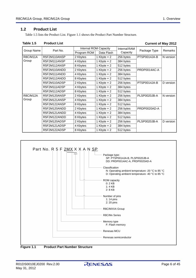
1.2 Product ListTable 1.5 lists the Product List. Figure 1.1 shows the Product Part Number Structure.
Figure 1.1 Product Part Number Structure
Table 1.5 Product List
Group Name Part No.Internal ROM Capacity Internal RAM
Capacity Package Type RemarksProgram ROM Data Flash
R8C/M11A Group
R5F2M110ANSP 2 Kbytes 1 Kbyte × 2 256 bytes PTSP0014JA-B N versionR5F2M111ANSP 4 Kbytes 1 Kbyte × 2 384 bytesR5F2M112ANSP 8 Kbytes 1 Kbyte × 2 512 bytesR5F2M110ANDD 2 Kbytes 1 Kbyte × 2 256 bytes PRDP0014AC-AR5F2M111ANDD 4 Kbytes 1 Kbyte × 2 384 bytesR5F2M112ANDD 8 Kbytes 1 Kbyte × 2 512 bytesR5F2M110ADSP 2 Kbytes 1 Kbyte × 2 256 bytes PTSP0014JA-B D versionR5F2M111ADSP 4 Kbytes 1 Kbyte × 2 384 bytesR5F2M112ADSP 8 Kbytes 1 Kbyte × 2 512 bytes
R8C/M12A Group
R5F2M120ANSP 2 Kbytes 1 Kbyte × 2 256 bytes PLSP0020JB-A N versionR5F2M121ANSP 4 Kbytes 1 Kbyte × 2 384 bytesR5F2M122ANSP 8 Kbytes 1 Kbyte × 2 512 bytesR5F2M120ANDD 2 Kbytes 1 Kbyte × 2 256 bytes PRDP0020AD-AR5F2M121ANDD 4 Kbytes 1 Kbyte × 2 384 bytesR5F2M122ANDD 8 Kbytes 1 Kbyte × 2 512 bytesR5F2M120ADSP 2 Kbytes 1 Kbyte × 2 256 bytes PLSP0020JB-A D versionR5F2M121ADSP 4 Kbytes 1 Kbyte × 2 384 bytesR5F2M122ADSP 8 Kbytes 1 Kbyte × 2 512 bytes
Current of May 2012
Part No. R 5 F 2MX X X A N SPPackage type:
SP: PTSP0014JA-B, PLSP0020JB-ADD: PRDP0014AC-A, PRDP0020AD-A
ClassificationN: Operating ambient temperature -20 °C to 85 °CD: Operating ambient temperature -40 °C to 85 °C
ROM capacity0: 2 KB1: 4 KB2: 8 KB
Number of pins1: 14 pins2: 20 pins
R8C/MXXA Group
R8C/Mx Series
Memory typeF: Flash memory
Renesas MCU
Renesas semiconductor

R8C/M11A Group, R8C/M12A Group 1. Overview
R01DS0010EJ0200 Rev.2.00 Page 7 of 45May 31, 2012
1.3 Block DiagramFigure 1.2 shows the Block Diagram.
Figure 1.2 Block Diagram
I/O ports
Watchdog timer(14 bits)
System clock generationcircuit
XIN-XOUTHigh-speed on-chip oscillatorLow-speed on-chip oscillator
Timers
Timer RJ2 (16 bits × 1)Timer RB2 (8 bits × 1
or 16 bits × 1)Timer RC (16 bits × 1)
A/D converter(10 bits × 6 channels)
UART
Clock synchronous serial I/OClock asynchronous serial I/O
Peripheral functions
Voltage detection circuit
RAM (2)
Multiplier
SBUSP
INTBISP
FLGPC
R8C CPU core Memory
ROM (1)R0HR1H
R2R3
R0LR1L
A0
FBA1
Notes:1. ROM size varies with the product.2. RAM size varies with the product.
Port P1
8
Port P3
4
Port P4
4
Comparator B
Port PA
1

R8C/M11A Group, R8C/M12A Group 1. Overview
R01DS0010EJ0200 Rev.2.00 Page 8 of 45May 31, 2012
1.4 Pin AssignmentFigures 1.3 and 1.4 show Pin Assignment (Top View). Table 1.6 lists the Pin Name Information by Pin Number.
Figure 1.3 R8C/M11A Group Pin Assignment (Top View)
Figure 1.4 R8C/M12A Group Pin Assignment (Top View)
3
4
6
7
P3_7/ADTRG/TRJO/TRCIOD
RESET/PA_0
P4_7/XOUT/INT2
VSS/AVSS
P4_6/XIN/RXD0/TXD0/INT1/VCOUT1/TRJIO
VCC/AVCC
MODE
14
13
12
11
10
9
8
P1_1/AN1/TRCIOA/TRCTRG/KI1
P1_2/AN2/TRCIOB/KI2
P1_3/AN3/TRCIOC/KI3/TRBO
P1_4/AN4/TXD0/RXD0/INT0/TRCIOB
P1_5/RXD0/TRJIO/INT1/VCOUT1
P1_6/IVREF1/CLK0/TRJO/TRCIOB
P1_7/AN7/IVCMP1/INT1/TRJIO/TRCCLK
R8C/M11A Group
PTSP0014JA-BPRDP0014AC-A
(Top view)
1
2
5
Note:1. Confirm the pin 1 position on the package by referring to Package Dimensions.
6
P4_2/TRBO/TXD0/KI3
P3_7/ADTRG/TRJO/TRCIOD
RESET/PA_0
P4_7/XOUT/INT2
VSS/AVSS
P4_6/XIN/RXD0/TXD0/INT1/VCOUT1/TRJIO
VCC/AVCC
MODE
P3_5/TRCIOD/KI2/VCOUT3
P3_4/IVREF3/TRCIOC/INT2
20
19
18
17
16
15
14
13
12
11
P1_0/AN0/TRCIOD/KI0
P1_1/AN1/TRCIOA/TRCTRG/KI1
P1_2/AN2/TRCIOB/KI2
P1_3/AN3/TRCIOC/KI3/TRBO
P1_4/AN4/TXD0/RXD0/INT0/TRCIOB
P1_5/RXD0/TRJIO/INT1/VCOUT1
P1_6/IVREF1/CLK0/TRJO/TRCIOB
P1_7/AN7/IVCMP1/INT1/TRJIO/TRCCLK
P4_5/INT0/ADTRG
P3_3/IVCMP3/TRCCLK/INT3
1
2
3
4
5
7
8
9
10
R8C/M12A Group
PLSP0020JB-APRDP0020AD-A
(Top view)
Note:1. Confirm the pin 1 position on the package by referring to Package Dimensions.

R8C/M11A Group, R8C/M12A Group 1. Overview
R01DS0010EJ0200 Rev.2.00 Page 9 of 45May 31, 2012
Table 1.6 Pin Name Information by Pin NumberPin Number
Control Pin PortI/O Pins for Peripheral Functions
R8C/M11A Group
R8C/M12A Group Interrupt Timer Serial
InterfaceA/D Converter, Comparator B
1 P4_2 KI3 TRBO TXD0
1 2 P3_7 TRJO/TRCIOD ADTRG2 3 RESET PA_0
3 4 XOUT P4_7 INT24 5 VSS/AVSS5 6 XIN P4_6 INT1 TRJIO RXD0/TXD0 VCOUT1
6 7 VCC/AVCC7 8 MODE
9 P3_5 KI2 TRCIOD VCOUT3
10 P3_4 INT2 TRCIOC IVREF3
11 P3_3 INT3 TRCCLK IVCMP3
12 P4_5 INT0 ADTRG8 13 P1_7 INT1 TRJIO/TRCCLK AN7/IVCMP1
9 14 P1_6 TRJO/TRCIOB CLK0 IVREF110 15 P1_5 INT1 TRJIO RXD0 VCOUT1
11 16 P1_4 INT0 TRCIOB RXD0/TXD0 AN4
12 17 P1_3 KI3 TRBO/TRCIOC AN3
13 18 P1_2 KI2 TRCIOB AN2
14 19 P1_1 KI1 TRCIOA/TRCTRG AN1
20 P1_0 KI0 TRCIOD AN0

R8C/M11A Group, R8C/M12A Group 1. Overview
R01DS0010EJ0200 Rev.2.00 Page 10 of 45May 31, 2012
1.5 Pin FunctionsTable 1.7 lists the Pin Functions.
Note:1. Contact the oscillator manufacturer for oscillation characteristics.
Table 1.7 Pin FunctionsItem Pin Name I/O Description
Power supply input VCC, VSS — Apply 1.8 V through 5.5 V to the VCC pin.Apply 0 V to the VSS pin.
Analog power supply input
AVCC, AVSS — Power supply input for the A/D converter.Connect a capacitor between pins AVCC and AVSS.
Reset input RESET I Applying a low level to this pin resets the MCU.
MODE MODE I Connect this pin to the VCC pin via a resistor.XIN clock input XIN I I/O for the XIN clock generation circuit.
Connect a ceramic resonator or a crystal oscillator between pins XIN and XOUT. (1)
To use an external clock, input it to the XIN pin. P4_7 can be used as an I/O port at this time.
XIN clock output XOUT O
INT interrupt input INT0 to INT3 I INT interrupt input.Key input interrupt KI0 to KI3 I Key input interrupt input.
I/O ports P1_0 to P1_7, P3_0 to P3_5, P3_7, P4_2, P4_5 to P4_7, PA_0
I/O CMOS I/O ports.Each port has an I/O select direction register, enabling switching input and output for each port.For input ports other than PA_0, the presence or absence of a pull-up resistor can be selected by a program.P1_2 to P1_5, P3_3 to P3_5, and P3_7 can be used as LED drive ports.
Timer RJ2 TRJIO I/O Timer RJ2 I/O.TRJO O Timer RJ2 output.
Timer RB2 TRBO O Timer RB2 output.Timer RC TRCCLK I External clock input.
TRCTRG I External trigger input.TRCIOA, TRCIOB, TRCIOC, TRCIOD
I/O Timer RC I/O.
Serial interface CLK0 I/O Transfer clock I/O.RXD0 I Serial data input.TXD0 O Serial data output.
A/D converter AN0 to AN4, AN7 I Analog input for the A/D converter.
ADTRG I External trigger input for the A/D converter.
Comparator B IVCMP1, IVCMP3 I Analog voltage input for comparator B.IVREF1, IVREF3 I Reference voltage input for comparator B.VCOUT1, VCOUT3 O Comparison result output for comparator B.

R8C/M11A Group, R8C/M12A Group 2. Central Processing Unit (CPU)
R01DS0010EJ0200 Rev.2.00 Page 11 of 45May 31, 2012
2. Central Processing Unit (CPU)Figure 2.1 shows the 13 CPU Registers. The registers, R0, R1, R2, R3, A0, A1, and FB form a single register bank.The CPU has two register banks.
Figure 2.1 CPU Registers
The higher 4 bits of INTB are INTBH andthe lower 16 bits of INTB are INTBL.
Interrupt table register
Data registers (1)
Address registers (1)
Frame base register (1)
User stack pointer
Interrupt stack pointer
Static base register
Program counter
Carry flag
Debug flag
Zero flag
Sign flag
Register bank select flag
Overflow flag
Interrupt enable flag
Stack pointer select flag
Reserved bits
Processor interrupt priority level
Reserved bit
Note:1. These registers form a single register bank.
The CPU has two register banks.
Flag register
R3R2
b31 b0b15
FB
R2R3A0A1
R0H (R0 high-order byte)
R1H (R1 high-order byte)
R0L (R0 low-order byte)
R1L (R1 low-order byte)
INTBHb19 b0
INTBLb15
PCb19 b0
b15 b0
USPISPSB
b15 b0
FLG
b15 b0b8 b7
CDZSBOIUIPL
b8 b7

R8C/M11A Group, R8C/M12A Group 2. Central Processing Unit (CPU)
R01DS0010EJ0200 Rev.2.00 Page 12 of 45May 31, 2012
2.1 Data Registers (R0, R1, R2, and R3)R0 is a 16-bit register for transfer, arithmetic, and logic operations. The same applies to R1 through R3. R0 can be split into high-order (R0H) and low-order (R0L) registers to be used separately as 8-bit data registers.The same applies to R1H and R1L. R2 can be combined with R0 and used as a 32-bit data register (R2R0). In thesame way as with R0 and R2, R3 and R1 can be used as a 32-bit data register (R3R1).
2.2 Address Registers (A0 and A1)A0 is a 16-bit register for address register indirect addressing and address register relative addressing. It is alsoused for transfer, arithmetic, and logic operations. A1 functions in the same manner as A0. A1 can be combinedwith A0 and used as a 32-bit address register (A1A0).
2.3 Frame Base Register (FB)FB is a 16-bit register used for FB relative addressing.
2.4 Interrupt Table Register (INTB)INTB is a 20-bit register that indicates the start address of a relocatable interrupt vector table.
2.5 Program Counter (PC)PC is a 20-bit register that indicates the address of the next instruction to be executed.
2.6 User Stack Pointer (USP) and Interrupt Stack Pointer (ISP)The stack pointers (SP), USP and ISP, are each 16 bits wide. The U flag of the FLG register is used to switchbetween USP and ISP.
2.7 Static Base Register (SB)SB is a 16-bit register used for SB relative addressing.
2.8 Flag Register (FLG)FLG is an 11-bit register that indicates the CPU state.
2.8.1 Carry Flag (C)The C flag retains carry, borrow, or shift-out bits that have been generated in the arithmetic and logic unit.
2.8.2 Debug Flag (D)The D flag is for debugging only. It must only be set to 0.
2.8.3 Zero Flag (Z)The Z flag is set to 1 when an arithmetic operation results in 0. Otherwise it is set to 0.
2.8.4 Sign Flag (S)The S flag is set to 1 when an arithmetic operation results in a negative value. Otherwise it is set to 0.
2.8.5 Register Bank Select Flag (B)Register bank 0 is selected when the B flag is 0. Register bank 1 is selected when this flag is 1.
2.8.6 Overflow Flag (O)The O flag is set to 1 when an operation results in an overflow. Otherwise it is set to 0.

R8C/M11A Group, R8C/M12A Group 2. Central Processing Unit (CPU)
R01DS0010EJ0200 Rev.2.00 Page 13 of 45May 31, 2012
2.8.7 Interrupt Enable Flag (I)The I flag enables maskable interrupts. Interrupts are disabled when the I flag is 0, and are enabled when the Iflag is 1. The I flag is set to 0 when an interrupt request is acknowledged.
2.8.8 Stack Pointer Select Flag (U)ISP is selected when the U flag is 0. USP is selected when the U flag is 1. The U flag is set to 0 when a hardwareinterrupt request is acknowledged or the INT instruction for a software interrupt numbered from 0 to 31 isexecuted.
2.8.9 Processor Interrupt Priority Level (IPL)IPL is 3 bits wide and assigns eight processor interrupt priority levels from 0 to 7. If a requested interrupt hashigher priority than IPL, the interrupt is enabled. If IPL is set to levels from 2 to 7, all maskable interruptrequests are disabled.
2.8.10 Reserved BitThe write value must be 0. The read value is undefined.

R8C/M11A Group, R8C/M12A Group 3. Address Space
R01DS0010EJ0200 Rev.2.00 Page 14 of 45May 31, 2012
3. Address Space
3.1 Memory MapFigure 3.1 shows the Memory Map. The R8C/M11A Group and R8C/M12A Group have a 1-Mbyte address spacefrom addresses 00000h to FFFFFh. The internal ROM (program ROM) is allocated at lower addresses, beginningwith address 0FFFFh. For example, an 8-Kbyte internal ROM area is allocated at addresses 0E000h to 0FFFFh.The fixed interrupt vector table is allocated at addresses 0FFDCh to 0FFFFh. The start address of each interruptroutine is stored here.The internal ROM (data flash) is allocated at addresses 03000h to 037FFh.The internal RAM is allocated at higher addresses, beginning with address 00400h. For example, a 512-byteinternal RAM area is allocated at addresses 00400h to 005FFh. The internal RAM is used not only for data storagebut also as a stack area when a subroutine is called or when an interrupt request is acknowledged.Special function registers (SFRs) are allocated at addresses 00000h to 002FFh. Peripheral function control registersare allocated here. All unallocated spaces within the SFRs are reserved and cannot be accessed by users.
Figure 3.1 Memory Map
Notes:1. Data flash indicates block A (1 Kbyte) and block B (1 Kbyte).2. The blank areas are reserved. No access is allowed.
0XXXXh
00000h
Internal ROM(program ROM)
Internal RAM
SFR(See 3.2 Special
Function Registers(SFRs))
Internal ROM(data flash) (1)
Expanded area
002FFh
03000h
037FFh
0YYYYh
0FFFFh
FFFFFh
00400h
0FFFFh
0FFDCh
0FFD8h
Watchdog timer, oscillation stop detection, voltage monitor 1
Undefined instructionOverflow
BRK instructionAddress match
Single-step
(Reserved)(Reserved)
Reset
Reserved area
Part Number
R5F2M110ANSP, R5F2M110ANDD, R5F2M110ADSP,R5F2M120ANSP, R5F2M120ANDD, R5F2M120ADSP
R5F2M111ANSP, R5F2M111ANDD, R5F2M111ADSP,R5F2M121ANSP, R5F2M121ANDD, R5F2M121ADSP
R5F2M112ANSP, R5F2M112ANDD, R5F2M112ADSP,R5F2M122ANSP, R5F2M122ANDD, R5F2M122ADSP
Capacity Address 0YYYYh
2 Kbytes
4 Kbytes
8 Kbytes
0F800h
0F000h
0E000h
Internal ROMAddress 0XXXXhCapacity
256 bytes
384 bytes
512 bytes
004FFh
0057Fh
005FFh
Internal RAM

R8C/M11A Group, R8C/M12A Group 3. Address Space
R01DS0010EJ0200 Rev.2.00 Page 15 of 45May 31, 2012
3.2 Special Function Registers (SFRs)An SFR (special function register) is a control register for a peripheral function. Tables 3.1 to 3.8 list the SFRInformation. Table 3.9 lists the ID Code Area and Option Function Select Area.
Notes:1. The blank areas are reserved. No access is allowed.2. The MSTINI bit in the OFS2 register is 0.3. The MSTINI bit in the OFS2 register is 1.4. The CSPROINI bit in the OFS register is 0.5. The CSPROINI bit in the OFS register is 1.
Table 3.1 SFR Information (1) (1)
Address Register Name Symbol After Reset00000h00001h00002h00003h00004h00005h00006h00007h00008h00009h0000Ah0000Bh0000Ch0000Dh0000Eh0000Fh00010h Processor Mode Register 0 PM0 00h00011h00012h Module Standby Control Register MSTCR 00h (2)
01110111b (3)
00013h Protect Register PRCR 00h00014h00015h00016h Hardware Reset Protect Register HRPR 00h00017h00018h00019h0001Ah0001Bh0001Ch0001Dh0001Eh0001Fh00020h External Clock Control Register EXCKCR 00h00021h High-Speed/Low-Speed On-Chip Oscillator Control Register OCOCR 00h00022h System Clock f Control Register SCKCR 00h00023h System Clock f Select Register PHISEL 00h00024h Clock Stop Control Register CKSTPR 00h00025h Clock Control Register When Returning from Modes CKRSCR 00h00026h Oscillation Stop Detection Register BAKCR 00h00027h00028h00029h0002Ah0002Bh0002Ch0002Dh0002Eh0002Fh00030h Watchdog Timer Function Register RISR 10000000b (4)
00h (5)
00031h Watchdog Timer Reset Register WDTR XXh00032h Watchdog Timer Start Register WDTS XXh00033h Watchdog Timer Control Register WDTC 01XXXXXXb00034h Count Source Protection Mode Register CSPR 10000000b (4)
00h (5)
00035h Periodic Timer Interrupt Control Register WDTIR 00h00036h00037h00038h External Input Enable Register INTEN 00h00039h

R8C/M11A Group, R8C/M12A Group 3. Address Space
R01DS0010EJ0200 Rev.2.00 Page 16 of 45May 31, 2012
X: UndefinedNotes:
1. The blank areas are reserved. No access is allowed.2. The LVDAS bit in the OFS register is 0.3. The LVDAS bit in the OFS register is 1.4. The value after a reset differs depending on the reset source.
Table 3.2 SFR Information (2) (1)
Address Register Name Symbol After Reset0003Ah INT Input Filter Select Register 0 INTF0 00h0003Bh0003Ch INT Input Edge Select Register 0 ISCR0 00h0003Dh0003Eh Key Input Enable Register KIEN 00h0003Fh00040h Interrupt Priority Level Register 0 ILVL0 00h00041h00042h Interrupt Priority Level Register 2 ILVL2 00h00043h Interrupt Priority Level Register 3 ILVL3 00h00044h Interrupt Priority Level Register 4 ILVL4 00h00045h Interrupt Priority Level Register 5 ILVL5 00h00046h Interrupt Priority Level Register 6 ILVL6 00h00047h Interrupt Priority Level Register 7 ILVL7 00h00048h Interrupt Priority Level Register 8 ILVL8 00h00049h Interrupt Priority Level Register 9 ILVL9 00h0004Ah Interrupt Priority Level Register A ILVLA 00h0004Bh Interrupt Priority Level Register B ILVLB 00h0004Ch Interrupt Priority Level Register C ILVLC 00h0004Dh Interrupt Priority Level Register D ILVLD 00h0004Eh Interrupt Priority Level Register E ILVLE 00h0004Fh00050h Interrupt Monitor Flag Register 0 IRR0 00h00051h Interrupt Monitor Flag Register 1 IRR1 00h00052h Interrupt Monitor Flag Register 2 IRR2 00h00053h External Interrupt Flag Register IRR3 00h00054h00055h00056h00057h00058h Voltage Monitor Circuit Edge Select Register VCAC 00h00059h0005Ah Voltage Detect Register 2 VCA2 00100100b (2)
00000100b (3)
0005Bh Voltage Detection 1 Level Select Register VD1LS 00000111b0005Ch Voltage Monitor 0 Circuit Control Register VW0C 1100X011b (2)
1100X010b (3)
0005Dh Voltage Monitor 1 Circuit Control Register VW1C 10001010b0005Eh0005Fh Reset Source Determination Register RSTFR 0000XXXXb (4)
00060h00061h00062h00063h00064h High-Speed On-Chip Oscillator 18.432 MHz Control Register 0 FR18S0 Value when shipped00065h High-Speed On-Chip Oscillator 18.432 MHz Control Register 1 FR18S1 Value when shipped00066h00067h High-Speed On-Chip Oscillator Control Register 1 FRV1 Value when shipped00068h High-Speed On-Chip Oscillator Control Register 2 FRV2 Value when shipped00069h0006Ah0006Bh0006Ch0006Dh0006Eh0006Fh00070h00071h00072h00073h00074h00075h00076h00077h00078h00079h

R8C/M11A Group, R8C/M12A Group 3. Address Space
R01DS0010EJ0200 Rev.2.00 Page 17 of 45May 31, 2012
X: UndefinedNote:
1. The blank areas are reserved. No access is allowed.
Table 3.3 SFR Information (3) (1)
Address Register Name Symbol After Reset0007Ah0007Bh0007Ch0007Dh0007Eh0007Fh00080h UART0 Transmit/Receive Mode Register U0MR 00h00081h UART0 Bit Rate Register U0BRG XXh00082h UART0 Transmit Buffer Register U0TBL XXh00083h U0TBH XXh00084h UART0 Transmit/Receive Control Register 0 U0C0 00001000b00085h UART0 Transmit/Receive Control Register 1 U0C1 00000010b00086h UART0 Receive Buffer Register U0RBL XXh00087h U0RBH XXh00088h UART0 Interrupt Flag and Enable Register U0IR 00h00089h0008Ah0008Bh0008Ch0008Dh0008Eh0008Fh00090h00091h00092h00093h00094h00095h00096h00097h00098h A/D Register 0 AD0L XXh00099h AD0H 000000XXb0009Ah A/D Register 1 AD1L XXh0009Bh AD1H 000000XXb0009Ch A/D Mode Register ADMOD 00h0009Dh A/D Input Select Register ADINSEL 00h0009Eh A/D Control Register 0 ADCON0 00h0009Fh A/D Interrupt Control Status Register ADICSR 00h000A0h000A1h000A2h000A3h000A4h000A5h000A6h000A7h000A8h000A9h Port P1 Direction Register PD1 00h000AAh000ABh Port P3 Direction Register PD3 00h000ACh Port P4 Direction Register PD4 00h000ADh Port PA Direction Register PDA 00h000AEh000AFh Port P1 Register P1 00h000B0h000B1h Port P3 Register P3 00h000B2h Port P4 Register P4 00h000B3h Port PA Register PA 00h000B4h000B5h Pull-Up Control Register 1 PUR1 00h000B6h000B7h Pull-Up Control Register 3 PUR3 00h000B8h Pull-Up Control Register 4 PUR4 00h000B9h Port I/O Function Control Register PINSR 00h000BAh000BBh Drive Capacity Control Register 1 DRR1 00h000BCh000BDh Drive Capacity Control Register 3 DRR3 00h000BEh000BFh

R8C/M11A Group, R8C/M12A Group 3. Address Space
R01DS0010EJ0200 Rev.2.00 Page 18 of 45May 31, 2012
Notes:1. The blank areas are reserved. No access is allowed.2. The TCNT16 bit in the TRBMR register is 0.3. The TCNT16 bit in the TRBMR register is 1.
Table 3.4 SFR Information (4) (1)
Address Register Name Symbol After Reset000C0h000C1h Open-Drain Control Register 1 POD1 00h000C2h000C3h Open-Drain Control Register 3 POD3 00h000C4h Open-Drain Control Register 4 POD4 00h000C5h Port PA Mode Control Register PAMCR 00010001b000C6h000C7h000C8h Port 1 Function Mapping Register 0 PML1 00h000C9h Port 1 Function Mapping Register 1 PMH1 00h000CAh000CBh000CCh Port 3 Function Mapping Register 0 PML3 00h000CDh Port 3 Function Mapping Register 1 PMH3 00h000CEh Port 4 Function Mapping Register 0 PML4 00h000CFh Port 4 Function Mapping Register 1 PMH4 00h000D0h000D1h Port 1 Function Mapping Expansion Register PMH1E 00h000D2h000D3h000D4h000D5h Port 4 Function Mapping Expansion Register PMH4E 00h000D6h000D7h000D8h Timer RJ Counter Register TRJ FFh000D9h FFh000DAh Timer RJ Control Register TRJCR 00h000DBh Timer RJ I/O Control Register TRJIOC 00h000DCh Timer RJ Mode Register TRJMR 00h000DDh Timer RJ Event Select Register TRJISR 00h000DEh Timer RJ Interrupt Control Register TRJIR 00h000DFh000E0h Timer RB Control Register TRBCR 00h000E1h Timer RB One-Shot Control Register TRBOCR 00h000E2h Timer RB I/O Control Register TRBIOC 00h000E3h Timer RB Mode Register TRBMR 00h000E4h Timer RB Prescaler Register (2)
Timer RB Primary/Secondary Register (Lower 8 Bits) (3)TRBPRE FFh
000E5h Timer RB Primary Register (2)
Timer RB Primary Register (Higher 8 Bits) (3)TRBPR FFh
000E6h Timer RB Secondary Register (2)
Timer RB Secondary Register (Higher 8 Bits) (3)TRBSC FFh
000E7h Timer RB Interrupt Control Register TRBIR 00h000E8h Timer RC Counter TRCCNT 00h000E9h 00h000EAh Timer RC General Register A TRCGRA FFh000EBh FFh000ECh Timer RC General Register B TRCGRB FFh000EDh FFh000EEh Timer RC General Register C TRCGRC FFh000EFh FFh000F0h Timer RC General Register D TRCGRD FFh000F1h FFh000F2h Timer RC Mode Register TRCMR 01001000b000F3h Timer RC Control Register 1 TRCCR1 00h000F4h Timer RC Interrupt Enable Register TRCIER 01110000b000F5h Timer RC Status Register TRCSR 01110000b000F6h Timer RC I/O Control Register 0 TRCIOR0 10001000b000F7h Timer RC I/O Control Register 1 TRCIOR1 10001000b000F8h Timer RC Control Register 2 TRCCR2 00011000b000F9h Timer RC Digital Filter Function Select Register TRCDF 00h000FAh Timer RC Output Enable Register TRCOER 01111111b000FBh Timer RC A/D Conversion Trigger Control Register TRCADCR 11110000b000FCh Timer RC Waveform Output Manipulation Register TRCOPR 00h000FDh000FEh000FFh

R8C/M11A Group, R8C/M12A Group 3. Address Space
R01DS0010EJ0200 Rev.2.00 Page 19 of 45May 31, 2012
Note:1. The blank areas are reserved. No access is allowed.
Table 3.5 SFR Information (5) (1)
Address Register Name Symbol After Reset00100h00101h00102h00103h00104h00105h00106h00107h00108h00109h0010Ah0010Bh0010Ch0010Dh0010Eh0010Fh00110h00111h00112h00113h00114h00115h00116h00117h00118h00119h0011Ah0011Bh0011Ch0011Dh0011Eh0011Fh00120h00121h00122h00123h00124h00125h00126h00127h00128h00129h0012Ah0012Bh0012Ch0012Dh0012Eh0012Fh00130h00131h00132h00133h00134h00135h00136h00137h00138h00139h0013Ah0013Bh0013Ch0013Dh0013Eh0013Fh

R8C/M11A Group, R8C/M12A Group 3. Address Space
R01DS0010EJ0200 Rev.2.00 Page 20 of 45May 31, 2012
Note:1. The blank areas are reserved. No access is allowed.
Table 3.6 SFR Information (6) (1)
Address Register Name Symbol After Reset00140h00141h00142h00143h00144h00145h00146h00147h00148h00149h0014Ah0014Bh0014Ch0014Dh0014Eh0014Fh00150h00151h00152h00153h00154h00155h00156h00157h00158h00159h0015Ah0015Bh0015Ch0015Dh0015Eh0015Fh00160h00161h00162h00163h00164h00165h00166h00167h00168h00169h0016Ah0016Bh0016Ch0016Dh0016Eh0016Fh00170h00171h00172h00173h00174h00175h00176h00177h00178h00179h0017Ah0017Bh0017Ch0017Dh0017Eh0017Fh

R8C/M11A Group, R8C/M12A Group 3. Address Space
R01DS0010EJ0200 Rev.2.00 Page 21 of 45May 31, 2012
Note:1. The blank areas are reserved. No access is allowed.
Table 3.7 SFR Information (7) (1)
Address Register Name Symbol After Reset00180h Comparator B Control Register WCMPR 00h00181h Comparator B1 Interrupt Control Register WCB1INTR 00h00182h Comparator B3 Interrupt Control Register WCB3INTR 00h00183h00184h00185h00186h00187h00188h00189h0018Ah0018Bh0018Ch0018Dh0018Eh0018Fh00190h00191h00192h00193h00194h00195h00196h00197h00198h00199h0019Ah0019Bh0019Ch0019Dh0019Eh0019Fh001A0h001A1h001A2h001A3h001A4h001A5h001A6h001A7h001A8h001A9h Flash Memory Status Register FST 10000000b001AAh Flash Memory Control Register 0 FMR0 00h001ABh Flash Memory Control Register 1 FMR1 00h001ACh Flash Memory Control Register 2 FMR2 00h001ADh Flash Memory Refresh Control Register FREFR 00h001AEh001AFh001B0h001B1h001B2h001B3h001B4h001B5h001B6h001B7h001B8h001B9h001BAh001BBh001BCh001BDh001BEh001BFh

R8C/M11A Group, R8C/M12A Group 3. Address Space
R01DS0010EJ0200 Rev.2.00 Page 22 of 45May 31, 2012
Note:1. The blank areas are reserved. No access is allowed.
Table 3.8 SFR Information (8) (1)
Address Register Name Symbol After Reset001C0h Address Match Interrupt Register 0 AIADR0L 00h001C1h AIADR0M 00h001C2h AIADR0H 00h001C3h Address Match Interrupt Enable Register 0 AIEN0 00h001C4h Address Match Interrupt Register 1 AIADR1L 00h001C5h AIADR1M 00h001C6h AIADR1H 00h001C7h Address Match Interrupt Enable Register 1 AIEN1 00h001C8h001C9h001CAh001CBh001CCh001CDh001CEh001CFh001D0h001D1h001D2h001D3h001D4h001D5h001D6h001D7h001D8h001D9h001DAh001DBh001DCh001DDh001DEh001DFh001E0h001E1h001E2h001E3h001E4h001E5h001E6h001E7h001E8h001E9h001EAh001EBh001ECh001EDh001EEh001EFh001F0h001F1h001F2h001F3h001F4h001F5h001F6h001F7h001F8h001F9h001FAh001FBh001FCh001FDh001FEh001FFh

R8C/M11A Group, R8C/M12A Group 3. Address Space
R01DS0010EJ0200 Rev.2.00 Page 23 of 45May 31, 2012
Notes:1. The option function select area is allocated in the flash memory, not in the SFRs. Set appropriate values as ROM data by a program.
Do not perform an additional write to the option function select area. Erasure of the block including the option function select area causes theoption function select area to be set to FFh.When blank products are shipped, the option function select area is set to FFh. It is set to the written value after written by the user.When factory-programming products are shipped, the value of the option function select area is the value programmed by the user.
2. The ID code area is allocated in the flash memory, not in the SFRs. Set appropriate values as ROM data by a program. Do not perform an additional write to the ID code area. Erasure of the block including the ID code area causes the ID code area to be set to FFh.When blank products are shipped, the ID code areas are set to FFh. They are set to the written value after written by the user.When factory-programming products are shipped, the value of the ID code areas is the value programmed by the user.
Table 3.9 ID Code Area and Option Function Select AreaAddress Area Name Symbol After Reset
:0FFDBh Option Function Select Register 2 OFS2 (Note 1)
:0FFDFh ID1 (Note 2)
:0FFE3h ID2 (Note 2)
:0FFEBh ID3 (Note 2)
:0FFEFh ID4 (Note 2)
:0FFF3h ID5 (Note 2)
:0FFF7h ID6 (Note 2)
:0FFFBh ID7 (Note 2)
:0FFFFh Option Function Select Register OFS (Note 1)

R8C/M11A Group, R8C/M12A Group 4. Electrical Characteristics
R01DS0010EJ0200 Rev.2.00 Page 24 of 45May 31, 2012
4. Electrical Characteristics
Note:1. When the oscillation circuit is used: bits CKPT1 to CKPT0 in the EXCKCR register are set to 11b
When the oscillation circuit is not used: bits CKPT1 to CKPT0 in the EXCKCR register are set to any value other than 11b
Table 4.1 Absolute Maximum RatingsSymbol Parameter Condition Rated Value Unit
VCC/AVCC Power supply voltage -0.3 to 6.5 VVI Input voltage XIN XIN-XOUT oscillation on
(oscillation circuit used) (1)-0.3 to 1.9 V
XIN-XOUT oscillation off (oscillation circuit not used) (1)
-0.3 to Vcc + 0.3 V
Other pins -0.3 to Vcc + 0.3 VVO Output voltage XOUT XIN-XOUT oscillation on
(oscillation circuit used) (1)-0.3 to 1.9 V
XIN-XOUT oscillation off (oscillation circuit not used) (1)
-0.3 to Vcc + 0.3 V
Other pins -0.3 to Vcc + 0.3 VPd Power consumption -40 °C ≤ Topr ≤ 85 °C 500 mWTopr Operating ambient temperature -20 to 85 (N version)/
-40 to 85 (D version)°C
Tstg Storage temperature -60 to 150 °C

R8C/M11A Group, R8C/M12A Group 4. Electrical Characteristics
R01DS0010EJ0200 Rev.2.00 Page 25 of 45May 31, 2012
Notes:1. Vcc = 1.8 V to 5.5 V and Topr = -20 °C to 85 °C (N version)/-40 °C to 85 °C (D version), unless otherwise specified.2. The average output current indicates the average value of current measured during 100 ms.3. For details, see Table 4.10 High-Speed On-Chip Oscillator Circuit Electrical Characteristics.4. For details, see Table 4.11 Low-Speed On-Chip Oscillator Circuit Electrical Characteristics.5. The pins with high drive capacity are P1_2, P1_3, P1_4, P1_5, P3_3, P3_4, P3_5, and P3_7.
Figure 4.1 Ports P1, P3, and P4 Timing Measurement Circuit
Table 4.2 Recommended Operating Conditions
Symbol Parameter ConditionStandard
UnitMin. Typ. Max.
VCC/AVCC Power supply voltage 1.8 — 5.5 VVSS/AVSS Power supply voltage — 0 — VVIH Input high voltage Other than CMOS input 0.8 Vcc — Vcc V
CMOS input 4.0 V ≤ Vcc ≤ 5.5 V 0.65 Vcc — Vcc V2.7 V ≤ Vcc < 4.0 V 0.7 Vcc — Vcc V1.8 V ≤ Vcc < 2.7 V 0.8 Vcc — Vcc V
VIL Input low voltage Other than CMOS input 0 — 0.2 Vcc VCMOS input 4.0 V ≤ Vcc ≤ 5.5 V 0 — 0.4 Vcc V
2.7 V ≤ Vcc < 4.0 V 0 — 0.3 Vcc V1.8 V ≤ Vcc < 2.7 V 0 — 0.2 Vcc V
IOH(sum) Peak sum output high current
Sum of all pins IOH(peak) — — -160 mA
IOH(sum) Average sum output high current
Sum of all pins IOH(avg) — — -80 mA
IOH(peak) Peak output high current When drive capacity is low — — -10 mAWhen drive capacity is high (5) — — -40 mA
IOH(avg) Average output high current When drive capacity is low — — -5 mAWhen drive capacity is high (5) — — -20 mA
IOL(sum) Peak sum output low current
Sum of all pins IOL(peak) — — 160 mA
IOL(sum) Average sum output low current
Sum of all pins IOL(avg) — — 80 mA
IOL(peak) Peak output low current When drive capacity is low — — 10 mAWhen drive capacity is high (5) — — 40 mA
IOL(avg) Average output low current When drive capacity is low — — 5 mAWhen drive capacity is high (5) — — 20 mA
f(XIN) XIN oscillation frequency 2.7 V ≤ Vcc ≤ 5.5 V 2 — 20 MHz1.8 V ≤ Vcc < 2.7 V 2 — 5 MHz
XIN clock input oscillation frequency 2.7 V ≤ Vcc ≤ 5.5 V 0 — 20 MHz1.8 V ≤ Vcc < 2.7 V 0 — 5 MHz
fHOCO High-speed on-chip oscillator oscillation frequency (3) 1.8 V ≤ Vcc ≤ 5.5 V — 20 — MHzfLOCO Low-speed on-chip oscillator oscillation frequency (4) 1.8 V ≤ Vcc ≤ 5.5 V — 125 — kHz— System clock frequency 2.7 V ≤ Vcc ≤ 5.5 V — — 20 MHz
1.8 V ≤ Vcc < 2.7 V — — 5 MHzfs CPU clock frequency 2.7 V ≤ Vcc ≤ 5.5 V 0 — 20 MHz
1.8 V ≤ Vcc < 2.7 V 0 — 5 MHz
P1P3P4 30 pF

R8C/M11A Group, R8C/M12A Group 4. Electrical Characteristics
R01DS0010EJ0200 Rev.2.00 Page 26 of 45May 31, 2012
Notes:1. Vcc/AVcc = 1.8 V to 5.5 V and Vss = 0 V and Topr = -20 °C to 85 °C (N version)/-40 °C to 85 °C (D version), unless otherwise
specified.2. The A/D conversion result will be undefined in stop mode, or when the flash memory is in low-current-consumption read mode
or stopped. Do not perform A/D conversion in these states. Do not enter these states during A/D conversion.
Notes:1. Vcc = 2.7 V to 5.5 V and Topr = -20 °C to 85 °C (N version)/-40 °C to 85 °C (D version), unless otherwise specified.2. When the digital filter is disabled.
Table 4.3 A/D Converter Characteristics
Symbol Parameter ConditionStandard
UnitMin. Typ. Max.
— Resolution — — 10 Bit— Absolute accuracy AVcc = 5.0 V AN0 to AN4, AN7 input — — ±3 LSB
AVcc = 3.0 V AN0 to AN4, AN7 input — — ±5 LSBAVcc = 1.8 V AN0 to AN4, AN7 input — — ±5 LSB
— A/D conversion clock 4.0 V ≤ AVcc ≤ 5.5 V (2) 2 — 20 MHz
3.2 V ≤ AVcc ≤ 5.5 V (2) 2 — 16 MHz
2.7 V ≤ AVcc ≤ 5.5 V (2) 2 — 10 MHz
1.8 V ≤ AVcc ≤ 5.5 V (2) 2 — 5 MHz— Permissible signal source
impedance3 kΩ
tCONV Conversion time AVcc = 5.0 V, A/D conversion clock = 20 MHz 2.20 — — µstSAMP Sampling time A/D conversion clock = 20 MHz 0.80 — — µsVIA Analog input voltage 0 — AVcc V
Table 4.4 Comparator B Electrical Characteristics
Symbol Parameter ConditionStandard
UnitMin. Typ. Max.
Vref IVREF1, IVREF3 input reference voltage 0 — Vcc - 1.4 VVI IVCMP1, IVCMP3 input voltage -0.3 — Vcc + 0.3 V— Offset — 5 100 mVtd Comparator output delay time (2) VI = Vref ± 100 mV — 0.1 — µsICMP Comparator operating current Vcc = 5.0 V — 17.5 — µA
R8C/M11A Group, R8C/M12A Group 4. Electrical Characteristics
R01DS0010EJ0200 Rev.2.00 Page 27 of 45May 31, 2012
Notes:1. Vcc = 2.7 V to 5.5 V and Topr = 0 °C to 60 °C, unless otherwise specified.2. Definition of program/erase endurance
The number of program/erase cycles is defined on a per-block basis. If the number of cycles is 10,000, each block can be erased 10,000 times. For example, if 1,024 cycles of 1-byte-write are performed to different addresses in 1 Kbyte of block A, and then the block iserased, the number of cycles is counted as one. Note, however, that the same address must not be programmed more thanonce before completion of an erase (overwriting prohibited).
3. This indicates the number of times up to which all electrical characteristics can be guaranteed after the last programming/erase operation. Operation is guaranteed for any number of operations in the range of 1 to the specified minimum (Min).
4. In a system that executes multiple programming operations, the actual erase count can be reduced by shifting the writeaddresses in sequence and programming so that as much of the flash memory as possible is used before performing an eraseoperation. For example, when programming in 16-byte units, the effective number of rewrites can be minimized byprogramming up to 128 units before erasing them all in one operation. It is also advisable to retain data on the number oferase operations for each block and establish a limit for the number of erase operations performed.
5. If an error occurs during a block erase, execute a clear status register command and then a block erase command at leastthree times until the erase error does not occur.
6. For information on the program/erase failure rate, contact a Renesas technical support representative.7. The data hold time includes the time that the power supply is off and the time the clock is not supplied.
Table 4.5 Flash Memory (Program ROM) Electrical Characteristics
Symbol Parameter ConditionStandard
UnitMin. Typ. Max.
— Program/erase endurance (2) 10,000 (3) — — times— Byte programming time
(program/erase endurance ≤ 1,000 times)
— 80 — µs
— Byte programming time (program/erase endurance > 1,000 times)
— 160 — µs
— Block erase time — 0.12 — std(SR-SUS) Transition time to suspend — — 0.25 + CPU clock
× 3 cyclesms
— Time from suspend until erase restart — — 30 + CPU clock × 1 cycle
µs
td(CMDRSTREADY)
Time from when command is forcibly terminated until reading is enabled
— — 30 + CPU clock × 1 cycle
µs
— Program/erase voltage 1.8 — 5.5 V— Read voltage 1.8 — 5.5 V— Program/erase temperature 0 — 60 °C— Data hold time (7) Ambient temperature = 85 °C 10 — — years

R8C/M11A Group, R8C/M12A Group 4. Electrical Characteristics
R01DS0010EJ0200 Rev.2.00 Page 28 of 45May 31, 2012
Notes:1. Vcc = 2.7 V to 5.5 V and Topr = -20 °C to 85 °C (N version)/-40 °C to 85 °C (D version), unless otherwise specified.2. Definition of program/erase endurance
The number of program/erase cycles is defined on a per-block basis. If the number of cycles is 10,000, each block can be erased 10,000 times. For example, if 1,024 cycles of 1-byte-write are performed to different addresses in 1 Kbyte of block A, and then the block iserased, the number of cycles is counted as one. Note, however, that the same address must not be programmed more thanonce before completion of an erase (overwriting prohibited).
3. This indicates the number of times up to which all electrical characteristics can be guaranteed after the last programming/erase operation. Operation is guaranteed for any number of operations in the range of 1 to the specified minimum (Min).
4. In a system that executes multiple program operations, the actual erase count can be reduced by shifting the write addressesin sequence and programming so that as much of the flash memory as possible is used before performing an erase operation.For example, when programming in 16-byte units, the effective number of rewrites can be minimized by programming up to128 units before erasing them all in one operation. It is also advisable to retain data on the number of erase operations foreach block and establish a limit for the number of erase operations performed.
5. If an error occurs during a block erase, execute a clear status register command and then a block erase command at leastthree times until the erase error does not occur.
6. For information on the program/erase failure rate, contact a Renesas technical support representative.7. The data hold time includes the time that the power supply is off and the time the clock is not supplied.
Figure 4.2 Transition Time until Suspend
Table 4.6 Flash Memory (Blocks A and B of Data Flash) Electrical Characteristics
Symbol Parameter ConditionStandard
UnitMin. Typ. Max.
— Program/erase endurance (2) 10,000 (3) — — times— Byte programming time — 150 — µs— Block erase time — 0.05 1 std(SR-SUS) Time delay from suspend request until
suspend— — 0.25 + CPU clock
× 3 cyclesms
— Time from suspend until erase restart — — 30 + CPU clock × 1 cycle
µs
td(CMDRST-READY)
Time from when command is forcibly stopped until reading is enabled
— — 30 + CPU clock × 1 cycle
µs
— Program/erase voltage 1.8 — 5.5 V— Read voltage 1.8 — 5.5 V— Program/erase temperature -20
(N version)— 85 °C
-40 (D version)
— 85 °C
— Data hold time (7) Ambient temperature = 85 °C 10 — — years
Suspend request(FMR21)
FST6, FST7: Bits in FST registerFMR21: Bit in FMR2 register
Fixed time
FST6Clock-dependent
time
td(SR-SUS)
Access restart
FST7

R8C/M11A Group, R8C/M12A Group 4. Electrical Characteristics
R01DS0010EJ0200 Rev.2.00 Page 29 of 45May 31, 2012
Notes:1. The measurement condition is Vcc = 1.8 V to 5.5 V and Topr = -20 °C to 85 °C (N version)/-40 °C to 85 °C (D version).2. Select the voltage detection level with bits VDSEL0 and VDSEL1 in the OFS register.3. The response time is from when the voltage passes Vdet0 until the voltage monitor 0 reset is generated.4. The wait time is necessary for the voltage detection circuit to operate when the VC0E bit in the VCA2 register is set to 0 and
then 1.
Notes:1. The measurement condition is Vcc = 1.8 V to 5.5 V and Topr = -20 °C to 85 °C (N version)/-40 °C to 85 °C (D version).2. Select the voltage detection level with bits VD1S1 to VD1S3 in the VD1LS register.3. The response time is from when the voltage passes Vdet1 until the voltage monitor 1 interrupt request is generated.4. The wait time is necessary for the voltage detection circuit to operate when the VC1E bit in the VCA2 register is set to 0 and
then 1.
Table 4.7 Voltage Detection 0 Circuit Electrical Characteristics
Symbol Parameter ConditionStandard
UnitMin. Typ. Max.
Vdet0 Voltage detection level Vdet0_0 (2) 1.80 1.90 2.05 V
Voltage detection level Vdet0_1 (2) 2.15 2.35 2.50 V
Voltage detection level Vdet0_2 (2) 2.70 2.85 3.05 V
Voltage detection level Vdet0_3 (2) 3.55 3.80 4.05 V— Voltage detection 0 circuit response time (3) When Vcc decreases from 5 V
to (Vdet0_0 - 0.1) V— 30 — µs
— Self power consumption in voltage detection circuit
VC0E = 1, Vcc = 5.0 V — 1.5 — µA
td(E-A) Wait time until voltage detection circuit operation starts (4)
— — 100 µs
Table 4.8 Voltage Detection 1 Circuit Electrical Characteristics
Symbol Parameter ConditionStandard
UnitMin. Typ. Max.
Vdet1 Voltage detection level Vdet1_1 (2) When Vcc decreases 2.15 2.35 2.55 V
Voltage detection level Vdet1_3 (2) When Vcc decreases 2.45 2.65 2.85 V
Voltage detection level Vdet1_5 (2) When Vcc decreases 2.75 2.95 3.15 V
Voltage detection level Vdet1_7 (2) When Vcc decreases 3.00 3.25 3.55 V
Voltage detection level Vdet1_9 (2) When Vcc decreases 3.30 3.55 3.85 V
Voltage detection level Vdet1_B (2) When Vcc decreases 3.60 3.85 4.15 V
Voltage detection level Vdet1_D (2) When Vcc decreases 3.90 4.15 4.45 V
Voltage detection level Vdet1_F (2) When Vcc decreases 4.20 4.45 4.75 V— Hysteresis width at the rising of Vcc in
voltage detection 1 circuitVdet1_1 to Vdet1_5 selected — 0.07 — VVdet1_7 to Vdet1_F selected — 0.10 — V
— Voltage detection 1 circuit response time (3) When Vcc decreases from 5 V to (Vdet1_0 - 0.1) V
— 60 150 µs
— Self power consumption in voltage detection circuit
VC1E = 1, Vcc = 5.0 V — 1.7 — µA
td(E-A) Wait time until voltage detection circuit operation starts (4)
— — 100 µs

R8C/M11A Group, R8C/M12A Group 4. Electrical Characteristics
R01DS0010EJ0200 Rev.2.00 Page 30 of 45May 31, 2012
Notes:1. The measurement condition is Topr = -20 °C to 85 °C (N version)/-40 °C to 85 °C (D version), unless otherwise specified.2. To use the power-on reset function, enable the voltage monitor 0 reset by setting the LVDAS bit in the OFS register to 0.
Figure 4.3 Power-On Reset Circuit Electrical Characteristics
Table 4.9 Power-On Reset Circuit (2)
Symbol Parameter ConditionStandard
UnitMin. Typ. Max.
trth External power Vcc rise gradient 0 — 50,000 mV/msec
Notes:1. Vdet0 indicates the voltage detection level of the voltage detection 0 circuit. For details, see 7. Voltage Detection Circuit
in the User’s Manual: Hardware.2. tw(por) is required for a power-on reset to be enabled with the external power Vcc held below the valid voltage (0.5 V) to
enable a power-on reset. When Vcc decreases with voltage monitor 0 reset disabled and then turns on, maintain tw(por) for1 ms or more.
Vdet0 (1)
Internal reset signal(low active)
0.5 V
tw(por) (2)
trth
Voltage detection 0circuit response time
External power Vcc
trth
× 2561fLOCO
× 2561fLOCO

R8C/M11A Group, R8C/M12A Group 4. Electrical Characteristics
R01DS0010EJ0200 Rev.2.00 Page 31 of 45May 31, 2012
Notes:1. Vcc = 1.8 V to 5.5 V, Topr = -20 °C to 85 °C (N version)/-40 °C to 85 °C (D version), unless otherwise specified.2. This enables the setting errors of bit rates such as 9600 bps and 38400 bps to be 0 % when the serial interface is used in
UART mode.
Note:1. Vcc = 1.8 V to 5.5 V, Topr = -20 °C to 85 °C (N version)/-40 °C to 85 °C (D version), unless otherwise specified.
Notes:1. The measurement condition is Vcc = 1.8 V to 5.5 V and Topr = 25 °C.2. Wait time until the internal power supply generation circuit stabilizes during power-on.
Table 4.10 High-Speed On-Chip Oscillator Circuit Electrical Characteristics
Symbol Parameter Package ConditionStandard
UnitMin. Typ. Max.
— High-speed on-chip oscillator frequency after reset is cleared
14-pin TSSOP20-pin LSSOP
Vcc = 1.8 V to 5.5 V, -20 °C ≤ Topr ≤ 85 °C
19.2 20.0 20.8 MHz
14-pin DIP20-pin DIP
19.0 20.0 21.0 MHz
14-pin TSSOP20-pin LSSOP
Vcc = 1.8 V to 5.5 V, -40 °C ≤ Topr ≤ 85 °C
19.0 20.0 21.0 MHz
High-speed on-chip oscillator frequency when the FR18S0 register adjustment value is written into the FRV1 register and the FR18S1 register adjustment value into the FRV2 register (2)
14-pin TSSOP20-pin LSSOP
Vcc = 1.8 V to 5.5 V, -20 °C ≤ Topr ≤ 85 °C
17.694 18.432 19.169 MHz
14-pin DIP20-pin DIP
17.510 18.432 19.353 MHz
14-pin TSSOP20-pin LSSOP
Vcc = 1.8 V to 5.5 V, -40 °C ≤ Topr ≤ 85 °C
17.510 18.432 19.353 MHz
— Oscillation stabilization time — — — 30 µs— Self power consumption at
oscillation — Vcc = 5.0 V, Topr = 25 °C — 530 — µA
Table 4.11 Low-Speed On-Chip Oscillator Circuit Electrical Characteristics
Symbol Parameter ConditionStandard
UnitMin. Typ. Max.
fLOCO Low-speed on-chip oscillator frequency 60 125 250 kHz— Oscillation stabilization time — — 35 µs— Self power consumption at oscillation Vcc = 5.0 V, Topr = 25 °C — 2 — µA
Table 4.12 Power Supply Circuit Timing Characteristics
Symbol Parameter ConditionStandard
UnitMin. Typ. Max.
td(P-R) Time for internal power supply stabilization during power-on (2)
— — 2,000 µs

R8C/M11A Group, R8C/M12A Group 4. Electrical Characteristics
R01DS0010EJ0200 Rev.2.00 Page 32 of 45May 31, 2012
Notes:1. 4.0 V ≤ Vcc ≤ 5.5 V and Topr = -20 °C to 85 °C (N version)/-40 °C to 85 °C (D version), f(XIN) = 20 MHz, unless otherwise
specified.2. High drive capacity can also be used while the peripheral output function is used.
Table 4.13 DC Characteristics (1) [4.0 V ≤ Vcc ≤ 5.5 V]
Symbol Parameter ConditionStandard
UnitMin. Typ. Max.
VOH Output high voltage P1_2, P1_3, P1_4, P1_5, P3_3, P3_4, P3_5, P3_7 (2)
When drive capacity is high
IOH = -20 mA Vcc - 2.0 — Vcc V
When drive capacity is low
IOH = -5 mA Vcc - 2.0 — Vcc V
P1_0, P1_1, P1_6, P1_7, P4_2, P4_5, P4_6, P4_7, PA_0
IOH = -5 mA Vcc - 2.0 — Vcc V
VOL Output low voltage P1_2, P1_3, P1_4, P1_5, P3_3, P3_4, P3_5, P3_7 (2)
When drive capacity is high
IOL = 20 mA — — 2.0 V
When drive capacity is low
IOL = 5 mA — — 2.0 V
P1_0, P1_1, P1_6, P1_7, P4_2, P4_5, P4_6, P4_7, PA_0
IOL = 5 mA — — 2.0 V
VT+-VT- Hysteresis INT0, INT1, INT2, INT3, KI0, KI1, KI2, KI3, TRJIO, TRCIOA, TRCIOB, TRCIOC, TRCIOD, RXD0, CLK0
Vcc = 5 V 0.1 1.2 — V
RESET Vcc = 5 V 0.1 1.2 — V
IIH Input high current VI = 5 V, Vcc = 5.0 V — — 5.0 µAIIL Input low current VI = 0 V, Vcc = 5.0 V — — -5.0 µARPULLUP Pull-up resistance VI = 0 V, Vcc = 5.0 V 25 50 100 kΩRfXIN Feedback resistance XIN — 2.2 — MΩVRAM RAM hold voltage In stop mode 1.8 — — V

R8C/M11A Group, R8C/M12A Group 4. Electrical Characteristics
R01DS0010EJ0200 Rev.2.00 Page 33 of 45May 31, 2012
Notes:1. Vcc = 4.0 V to 5.5 V, single-chip mode, output pins are open, and other pins are connected to Vss.2. When the XIN input is a square wave.3. Vcc = 5.0 V4. Set the system clock to 4 MHz with the PHISEL register.
Table 4.14 DC Characteristics (2) [4.0 V ≤ Vcc ≤ 5.5 V](Topr = -20 °C to 85 °C (N version)/-40 °C to 85 °C (D version), unless otherwise specified)
Symbol Parameter
Condition
UnitOscillation
Circuit On-Chip OscillatorCPU Clock
Low-Power-Consumption
SettingOther
Standard
XIN (2) High-Speed
Low-Speed Min. Typ. (3) Max.
ICC Power supply current (1)
High-speed clock mode
20 MHz Off 125 kHz No division
— — 3 7.0 mA
16 MHz Off 125 kHz No division
— — 2.5 6.0 mA
10 MHz Off 125 kHz No division
— — 1.7 — mA
20 MHz Off 125 kHz Division by 8
— — 1.5 — mA
16 MHz Off 125 kHz Division by 8
— — 1.2 — mA
10 MHz Off 125 kHz Division by 8
— — 1.0 — mA
High-speed on-chip oscillator mode
Off 20 MHz 125 kHz No division
— 3.5 7.5 mA
Off 20 MHz 125 kHz Division by 8
— 2.0 — mA
Off 4 MHz (4) 125 kHz Division by 16
MSTTRC = 1 — 1.0 — mA
Low-speed on-chip oscillator mode
Off Off 125 kHz Division by 8
FMR27 = 1LPE = 0
— 60 270 µA
Wait mode Off Off 125 kHz — VC1E = 0VC0E = 0LPE = 1
Peripheral clock supplied during WAIT instruction execution
— 15 100 µA
Off Off 125 kHz — VC1E = 0VC0E = 0LPE = 1WCKSTP = 1
Peripheral clock stopped during WAIT instruction execution
— 4.0 90 µA
Stop mode Off Off Off — VC1E = 0VC0E = 0STPM = 1
Topr = 25 °CPeripheral clock stopped
— 1.0 4.0 µA
Off Off Off — VC1E = 0VC0E = 0STPM = 1
Topr = 85 °CPeripheral clock stopped
— 1.5 — µA

R8C/M11A Group, R8C/M12A Group 4. Electrical Characteristics
R01DS0010EJ0200 Rev.2.00 Page 34 of 45May 31, 2012
Timing Requirements (Vcc = 5 V, Vss = 0 V at Topr = 25 °C, unless otherwise specified)
Figure 4.4 External Clock Input Timing When Vcc = 5 V
Figure 4.5 TRJIO Input Timing When Vcc = 5 V
Table 4.15 External Clock Input (XIN)
Symbol ParameterStandard
UnitMin. Max.
tc(XIN) XIN input cycle time 50 — nstWH(XIN) XIN input high width 24 — nstWL(XIN) XIN input low width 24 — ns
Table 4.16 TRJIO Input
Symbol ParameterStandard
UnitMin. Max.
tc(TRJIO) TRJIO input cycle time 100 — nstWH(TRJIO) TRJIO input high width 40 — nstWL(TRJIO) TRJIO input low width 40 — ns
Vcc = 5 V
ExternalClock input
tWH(XIN)
tC(XIN)
tWL(XIN)
Vcc = 5 V
TRJIO input
tWH(TRJIO)
tC(TRJIO)
tWL(TRJIO)

R8C/M11A Group, R8C/M12A Group 4. Electrical Characteristics
R01DS0010EJ0200 Rev.2.00 Page 35 of 45May 31, 2012
Figure 4.6 Serial Interface Timing When Vcc = 5 V
Notes:1. When the digital filter is enabled by the INTi input filter select bit, the INTi input high width is (1/digital filter clock frequency × 3)
or the minimum value of the standard, whichever is greater.2. When the digital filter is enabled by the INTi input filter select bit, the INTi input low width is (1/digital filter clock frequency × 3)
or the minimum value of the standard, whichever is greater.
Figure 4.7 Timing for External Interrupt INTi Input and Key Input Interrupt KIi When Vcc = 5 V
Table 4.17 Serial Interface
Symbol ParameterStandard
UnitMin. Max.
tc(CK) CLK0 input cycle time 200 — nstW(CKH) CLK0 input high width 100 — nstW(CKL) CLK0 input low width 100 — nstd(C-Q) TXD0 output delay time — 50 nsth(C-Q) TXD0 hold time 0 — nstsu(D-C) RXD0 input setup time 50 — nsth(C-D) RXD0 input hold time 90 — ns
Table 4.18 External Interrupt INTi Input, Key Input Interrupt KIi (i = 0 to 3)
Symbol ParameterStandard
UnitMin. Max.
tW(INH) INTi input high width, KIi input high width 250 (1) — ns
tW(INL) INTi input low width, KIi input low width 250 (2) — ns
Vcc = 5 V
CLK0
tW(CKH)
tC(CK)
tW(CKL)
TXD0
RXD0
tsu(D-C)td(C-Q)th(C-D)
th(C-Q)
Vcc = 5 V
INTi inputKIi input
(i = 0 to 3)
tW(INL)
tW(INH)

R8C/M11A Group, R8C/M12A Group 4. Electrical Characteristics
R01DS0010EJ0200 Rev.2.00 Page 36 of 45May 31, 2012
Notes:1. 2.7 V ≤ Vcc < 4.0 V and Topr = -20 °C to 85 °C (N version)/-40 °C to 85 °C (D version), f(XIN) = 10 MHz, unless otherwise
specified.2. High drive capacity can also be used while the peripheral output function is used.
Table 4.19 DC Characteristics (3) [2.7 V ≤ Vcc < 4.0 V]
Symbol Parameter ConditionStandard
UnitMin. Typ. Max.
VOH Output high voltage P1_2, P1_3, P1_4, P1_5, P3_3, P3_4, P3_5, P3_7 (2)
When drive capacity is high
IOH = -5 mA Vcc - 0.5 — Vcc V
When drive capacity is low
IOH = -1 mA Vcc - 0.5 — Vcc V
P1_0, P1_1, P1_6, P1_7, P4_2, P4_5, P4_6, P4_7, PA_0
IOH = -1 mA Vcc - 0.5 — Vcc V
VOL Output low voltage P1_2, P1_3, P1_4, P1_5, P3_3, P3_4, P3_5, P3_7 (2)
When drive capacity is high
IOL = 5 mA — — 0.5 V
When drive capacity is low
IOL = 1 mA — — 0.5 V
P1_0, P1_1, P1_6, P1_7, P4_2, P4_5, P4_6, P4_7, PA_0
IOL = 1 mA — — 0.5 V
VT+-VT- Hysteresis INT0, INT1, INT2, INT3, KI0, KI1, KI2, KI3, TRJIO, TRCIOA, TRCIOB, TRCIOC, TRCIOD, RXD0, CLK0
Vcc = 3 V 0.1 0.4 — V
RESET Vcc = 3 V 0.1 0.5 — V
IIH Input high current VI = 3 V, Vcc = 3.0 V — — 4.0 µAIIL Input low current VI = 0 V, Vcc = 3.0 V — — -4.0 µARPULLUP Pull-up resistance VI = 0 V, Vcc = 3.0 V 42 84 168 kΩRfXIN Feedback resistance XIN — 2.2 — MΩVRAM RAM hold voltage In stop mode 1.8 — — V
R8C/M11A Group, R8C/M12A Group 4. Electrical Characteristics
R01DS0010EJ0200 Rev.2.00 Page 37 of 45May 31, 2012
Notes:1. Vcc = 2.7 V to 4.0 V, single-chip mode, output pins are open, and other pins are connected to Vss.2. When the XIN input is a square wave.3. Vcc = 3.0 V4. Set the system clock to 10 MHz or 4 MHz with the PHISEL register.
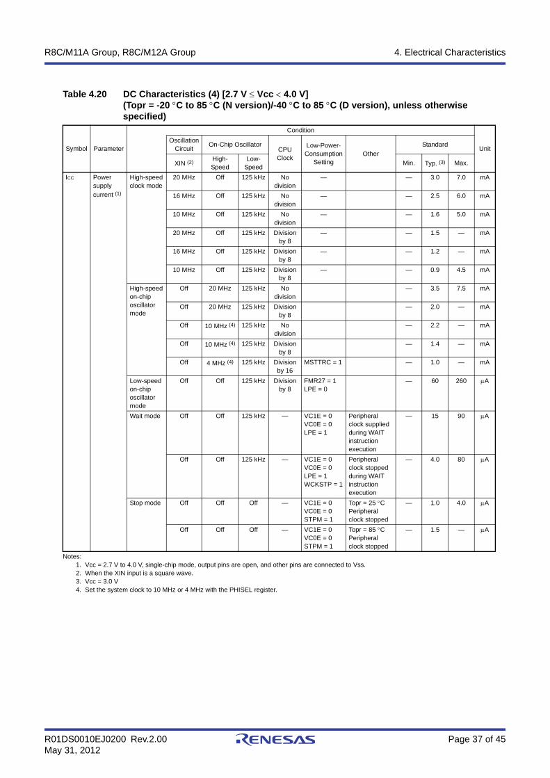
Table 4.20 DC Characteristics (4) [2.7 V ≤ Vcc < 4.0 V](Topr = -20 °C to 85 °C (N version)/-40 °C to 85 °C (D version), unless otherwise specified)
Symbol Parameter
Condition
UnitOscillation
Circuit On-Chip OscillatorCPU Clock
Low-Power-Consumption
SettingOther
Standard
XIN (2) High-Speed
Low-Speed Min. Typ. (3) Max.
ICC Power supply current (1)
High-speed clock mode
20 MHz Off 125 kHz No division
— — 3.0 7.0 mA
16 MHz Off 125 kHz No division
— — 2.5 6.0 mA
10 MHz Off 125 kHz No division
— — 1.6 5.0 mA
20 MHz Off 125 kHz Division by 8
— — 1.5 — mA
16 MHz Off 125 kHz Division by 8
— — 1.2 — mA
10 MHz Off 125 kHz Division by 8
— — 0.9 4.5 mA
High-speed on-chip oscillator mode
Off 20 MHz 125 kHz No division
— 3.5 7.5 mA
Off 20 MHz 125 kHz Division by 8
— 2.0 — mA
Off 10 MHz (4) 125 kHz No division
— 2.2 — mA
Off 10 MHz (4) 125 kHz Division by 8
— 1.4 — mA
Off 4 MHz (4) 125 kHz Division by 16
MSTTRC = 1 — 1.0 — mA
Low-speed on-chip oscillator mode
Off Off 125 kHz Division by 8
FMR27 = 1LPE = 0
— 60 260 µA
Wait mode Off Off 125 kHz — VC1E = 0VC0E = 0LPE = 1
Peripheral clock supplied during WAIT instruction execution
— 15 90 µA
Off Off 125 kHz — VC1E = 0VC0E = 0LPE = 1WCKSTP = 1
Peripheral clock stopped during WAIT instruction execution
— 4.0 80 µA
Stop mode Off Off Off — VC1E = 0VC0E = 0STPM = 1
Topr = 25 °CPeripheral clock stopped
— 1.0 4.0 µA
Off Off Off — VC1E = 0VC0E = 0STPM = 1
Topr = 85 °CPeripheral clock stopped
— 1.5 — µA

R8C/M11A Group, R8C/M12A Group 4. Electrical Characteristics
R01DS0010EJ0200 Rev.2.00 Page 38 of 45May 31, 2012
Timing Requirements (Vcc = 3 V, Vss = 0 V at Topr = 25 °C, unless otherwise specified)
Figure 4.8 External Clock Input Timing When Vcc = 3 V
Figure 4.9 TRJIO Input Timing When Vcc = 3 V
Table 4.21 External Clock Input (XIN)
Symbol ParameterStandard
UnitMin. Max.
tc(XIN) XIN input cycle time 50 — nstWH(XIN) XIN input high width 24 — nstWL(XIN) XIN input low width 24 — ns
Table 4.22 TRJIO Input
Symbol ParameterStandard
UnitMin. Max.
tc(TRJIO) TRJIO input cycle time 300 — nstWH(TRJIO) TRJIO input high width 120 — nstWL(TRJIO) TRJIO input low width 120 — ns
Vcc = 3 V
ExternalClock input
tWH(XIN)
tC(XIN)
tWL(XIN)
Vcc = 3 V
TRJIO input
tWH(TRJIO)
tC(TRJIO)
tWL(TRJIO)

R8C/M11A Group, R8C/M12A Group 4. Electrical Characteristics
R01DS0010EJ0200 Rev.2.00 Page 39 of 45May 31, 2012
Figure 4.10 Serial Interface Timing When Vcc = 3 V
Notes:1. When the digital filter is enabled by the INTi input filter select bit, the INTi input high width is (1/digital filter clock frequency × 3)
or the minimum value of the standard, whichever is greater.2. When the digital filter is enabled by the INTi input filter select bit, the INTi input low width is (1/digital filter clock frequency × 3)
or the minimum value of the standard, whichever is greater.
Figure 4.11 Timing for External Interrupt INTi Input and Key Input Interrupt KIi When Vcc = 3 V
Table 4.23 Serial Interface
Symbol ParameterStandard
UnitMin. Max.
tc(CK) CLK0 input cycle time 300 — nstW(CKH) CLK0 input high width 150 — nstW(CKL) CLK0 input low width 150 — nstd(C-Q) TXD0 output delay time — 80 nsth(C-Q) TXD0 hold time 0 — nstsu(D-C) RXD0 input setup time 70 — nsth(C-D) RXD0 input hold time 90 — ns
Table 4.24 External Interrupt INTi Input, Key Input Interrupt KIi (i = 0 to 3)
Symbol ParameterStandard
UnitMin. Max.
tW(INH) INTi input high width, KIi input high width 380 (1) — ns
tW(INL) INTi input low width, KIi input low width 380 (2) — ns
Vcc = 3 V
CLK0
tW(CKH)
tC(CK)
tW(CKL)
TXD0
RXD0
tsu(D-C)td(C-Q)th(C-D)
th(C-Q)
Vcc = 3 V
INTi inputKIi input
(i = 0 to 3)
tW(INL)
tW(INH)

R8C/M11A Group, R8C/M12A Group 4. Electrical Characteristics
R01DS0010EJ0200 Rev.2.00 Page 40 of 45May 31, 2012
Notes:1. 1.8 V ≤ Vcc < 2.7 V and Topr = -20 °C to 85 °C (N version)/-40 °C to 85 °C (D version), f(XIN) = 5 MHz, unless otherwise
specified.2. High drive capacity can also be used while the peripheral output function is used.
Table 4.25 DC Characteristics (5) [1.8 V ≤ Vcc < 2.7 V]
Symbol Parameter ConditionStandard
UnitMin. Typ. Max.
VOH Output high voltage P1_2, P1_3, P1_4, P1_5, P3_3, P3_4, P3_5, P3_7 (2)
When drive capacity is high
IOH = -2 mA Vcc - 0.5 — Vcc V
When drive capacity is low
IOH = -1 mA Vcc - 0.5 — Vcc V
P1_0, P1_1, P1_6, P1_7, P4_2, P4_5, P4_6, P4_7, PA_0
IOH = -1 mA Vcc - 0.5 — Vcc V
VOL Output low voltage P1_2, P1_3, P1_4, P1_5, P3_3, P3_4, P3_5, P3_7 (2)
When drive capacity is high
IOL = 2 mA — — 0.5 V
When drive capacity is low
IOL = 1 mA — — 0.5 V
P1_0, P1_1, P1_6, P1_7, P4_2, P4_5, P4_6, P4_7, PA_0
IOL = 1 mA — — 0.5 V
VT+-VT- Hysteresis INT0, INT1, INT2, INT3, KI0, KI1, KI2, KI3, TRJIO, TRCIOA, TRCIOB, TRCIOC, TRCIOD, RXD0, CLK0
Vcc = 2.2 V 0.05 0.20 — V
RESET Vcc = 2.2 V 0.05 0.20 — V
IIH Input high current VI = 2.2 V, Vcc = 2.2 V — — 4.0 µAIIL Input low current VI = 0 V, Vcc = 2.2 V — — -4.0 µARPULLUP Pull-up resistance VI = 0 V, Vcc = 2.2 V 70 140 300 kΩRfXIN Feedback resistance XIN — 2.2 — MΩVRAM RAM hold voltage In stop mode 1.8 — — V

R8C/M11A Group, R8C/M12A Group 4. Electrical Characteristics
R01DS0010EJ0200 Rev.2.00 Page 41 of 45May 31, 2012
Notes:1. Vcc = 1.8 V to 2.7 V, single-chip mode, output pins are open, and other pins are connected to Vss.2. When the XIN input is a square wave.3. Vcc = 2.2 V4. Set the system clock to 5 MHz or 4 MHz with the PHISEL register.
Table 4.26 DC Characteristics (6) [1.8 V ≤ Vcc < 2.7 V](Topr = -20 °C to 85 °C (N version)/-40 °C to 85 °C (D version), unless otherwise specified)
Symbol Parameter
Condition
UnitOscillation
Circuit On-Chip OscillatorCPU Clock
Low-Power-Consumption
SettingOther
Standard
XIN (2) High-Speed
Low-Speed Min. Typ. (3) Max.
ICC Power supply current (1)
High-speed clock mode
5 MHz Off 125 kHz No division
— — 1.0 — mA
5 MHz Off 125 kHz Division by 8
— — 0.6 — mA
High-speed on-chip oscillator mode
Off 5 MHz (4) 125 kHz No division
— 1.6 6.5 mA
Off 5 MHz (4) 125 kHz Division by 8
— 1.1 — mA
Off 4 MHz (4) 125 kHz Division by 16
MSTTRC = 1 — 1.0 — mA
Low-speed on-chip oscillator mode
Off Off 125 kHz Division by 8
FMR27 = 1LPE = 0
— 60 200 µA
Wait mode Off Off 125 kHz — VC1E = 0VC0E = 0LPE = 1
Peripheral clock supplied during WAIT instruction execution
— 15 90 µA
Off Off 125 kHz — VC1E = 0VC0E = 0LPE = 1WCKSTP = 1
Peripheral clock stopped during WAIT instruction execution
— 4.0 80 µA
Stop mode Off Off Off — VC1E = 0VC0E = 0STPM = 1
Topr = 25 °CPeripheral clock stopped
— 1.0 4.0 µA
Off Off Off — VC1E = 0VC0E = 0STPM = 1
Topr = 85 °CPeripheral clock stopped
— 1.5 — µA

R8C/M11A Group, R8C/M12A Group 4. Electrical Characteristics
R01DS0010EJ0200 Rev.2.00 Page 42 of 45May 31, 2012
Timing Requirements (Vcc = 2.2 V, Vss = 0 V at Topr = 25 °C, unless otherwise specified)
Figure 4.12 External Clock Input Timing When Vcc = 2.2 V
Figure 4.13 TRJIO Input Timing When Vcc = 2.2 V
Table 4.27 External Clock Input (XIN)
Symbol ParameterStandard
UnitMin. Max.
tc(XIN) XIN input cycle time 200 — nstWH(XIN) XIN input high width 90 — nstWL(XIN) XIN input low width 90 — ns
Table 4.28 TRJIO Input
Symbol ParameterStandard
UnitMin. Max.
tc(TRJIO) TRJIO input cycle time 500 — nstWH(TRJIO) TRJIO input high width 200 — nstWL(TRJIO) TRJIO input low width 200 — ns
Vcc = 2.2 V
ExternalClock input
tWH(XIN)
tC(XIN)
tWL(XIN)
Vcc = 2.2 V
TRJIO input
tWH(TRJIO)
tC(TRJIO)
tWL(TRJIO)
R8C/M11A Group, R8C/M12A Group 4. Electrical Characteristics
R01DS0010EJ0200 Rev.2.00 Page 43 of 45May 31, 2012
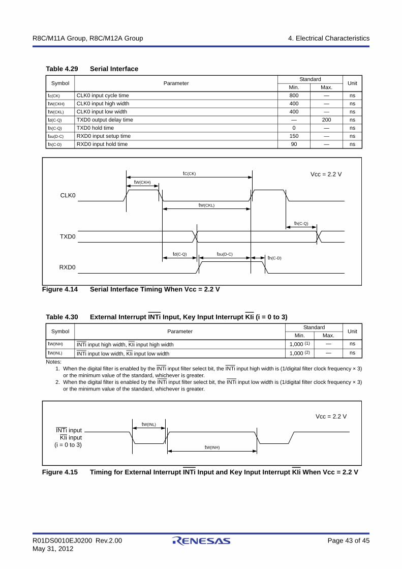
Figure 4.14 Serial Interface Timing When Vcc = 2.2 V
Notes:1. When the digital filter is enabled by the INTi input filter select bit, the INTi input high width is (1/digital filter clock frequency × 3)
or the minimum value of the standard, whichever is greater.2. When the digital filter is enabled by the INTi input filter select bit, the INTi input low width is (1/digital filter clock frequency × 3)
or the minimum value of the standard, whichever is greater.
Figure 4.15 Timing for External Interrupt INTi Input and Key Input Interrupt KIi When Vcc = 2.2 V
Table 4.29 Serial Interface
Symbol ParameterStandard
UnitMin. Max.
tc(CK) CLK0 input cycle time 800 — nstW(CKH) CLK0 input high width 400 — nstW(CKL) CLK0 input low width 400 — nstd(C-Q) TXD0 output delay time — 200 nsth(C-Q) TXD0 hold time 0 — nstsu(D-C) RXD0 input setup time 150 — nsth(C-D) RXD0 input hold time 90 — ns
Table 4.30 External Interrupt INTi Input, Key Input Interrupt KIi (i = 0 to 3)
Symbol ParameterStandard
UnitMin. Max.
tW(INH) INTi input high width, KIi input high width 1,000 (1) — ns
tW(INL) INTi input low width, KIi input low width 1,000 (2) — ns
Vcc = 2.2 V
CLK0
tW(CKH)
tC(CK)
tW(CKL)
TXD0
RXD0
tsu(D-C)td(C-Q)th(C-D)
th(C-Q)
Vcc = 2.2 V
INTi inputKIi input
(i = 0 to 3)
tW(INL)
tW(INH)

R8C/M11A Group, R8C/M12A Group Package Dimensions
R01DS0010EJ0200 Rev.2.00 Page 44 of 45May 31, 2012
Package DimensionsDiagrams showing the latest package dimensions and mounting information are available in the “Packages” section ofthe Renesas Electronics website.
NOTE)
1. DIMENSIONS"*1 (Nom)"AND"*2" DO NOT INCLUDE MOLD FLASH.
2. DIMENSION"*3"DOES NOT INCLUDE TRIM OFFSET.
Terminal cross section
(Ni/Pd/Au plating)
c
Detail F
L
Index mark
F
*1
*2
*3 bp
HE
Mx
1 7
14 8
S
S
y
e
Z
E
D
A
P-TSSOP14-4.4x5-0.65 0.05g
MASS[Typ.]
TTP-14DVPTSP0014JA-B
RENESAS CodeJEITA Package Code Previous Code
0.83
0.10
0.65
6.20 6.60
0.200.15
5.30
MaxNomMin
Dimension in MillimetersSymbol
Reference
1.10
0.60.50.4
4.40
0.100.070.03
0.25
0.200.150.10
6.40
8°0°
0.13
1.0
5.00
e
HE
L
A
D
E
A2
A1
bp
b1
c
xy
Z
L1
c1
θ
θ
L1
bp
A1
INCLUDE TRIM OFFSET.DIMENSION "*3" DOES NOT
NOTE)
DO NOT INCLUDE MOLD FLASH.DIMENSIONS "*1" AND "*2"1.
2.
e1
e
*2
*3
814
71
SEATING PLANE
*1
ZD bp
c
A1
E
b3
D
A2
AL
6.45
19.4
6.25
19.2
2.92
A2
L
e1
c
A1 0.5
A 4.8
E 6.35
D 19.3
7.69
ReferenceSymbol
Dimension in Millimeters
Min Nom Max
b3
bp 0.38 0.55
1.47 1.52 1.57
3.05 3.25 3.45
0.21 0.35
e 2.54θ 0° 15°
P-DIP14-6.35x19.3-2.54 0.94g
MASS[Typ.]
14P4X-APRDP0014AC-A
RENESAS CodeJEITA Package Code Previous Code
ZD 2.03
θ

R8C/M11A Group, R8C/M12A Group Package Dimensions
R01DS0010EJ0200 Rev.2.00 Page 45 of 45May 31, 2012
Index mark1 10
1120
F
*1
*3
*2
c
bpeA
D
E
HE
INCLUDE TRIM OFFSET.DIMENSION "*3" DOES NOT
NOTE)
DO NOT INCLUDE MOLD FLASH.DIMENSIONS "*1" AND "*2"1.
2.
Detail F
A1A2
L
0.320.220.17bp
Previous CodeJEITA Package Code RENESAS Code
PLSP0020JB-A 20P2F-A
MASS[Typ.]
0.1gP-LSSOP20-4.4x6.5-0.65
0.20.150.13
MaxNomMin
Dimension in Millimeters
SymbolReference
6.66.56.4D
4.54.44.3E
1.15A2
6.66.46.2
1.45A
0.20.10
0.70.50.3L
10°0°
c
0.65e
0.10y
HE
A1
0.53 0.77
y S
S
INCLUDE TRIM OFFSET.DIMENSION "*3" DOES NOT
NOTE)
DO NOT INCLUDE MOLD FLASH.DIMENSIONS "*1" AND "*2"1.
2.
7.1
26.9
6.1
24.9
2.9
0° 15°
A2
L
e1
c
A1 0.38
A 5.33
E 6.6
D 25.9
7.69
ReferenceSymbol
Dimension in Millimeters
Min Nom Max
b3
bp 0.36 0.46 0.56
1.32 1.52 1.72
3.1 3.3 3.5
0.21 0.35
e 2.54θ
P-DIP20-6.6x25.9-2.54 1.39g
MASS[Typ.]
20P4X-APRDP0020AD-A
RENESAS CodeJEITA Package Code Previous Code
ZD 1.52
θ
e
e1
*2
*3
1120
101
SEATING PLANE
*1
LA
ZD
A1
bp
c
E
b3
D
A2

C - 1
R8C/M11A Group, R8C/M12A Group Datasheet
Rev. DateDescription
Page Summary
0.01 Jan 14, 2010 — First Edition issued
0.10 Aug 25, 2010 — Document No. “REJ03B0308” → “R01DS0010EJ”
2, 3 1.1.2 Differences between Groups added
4 Table 1.3 “Reset by voltage detection 0” deleted
5 Table 1.4 “... ROM: VCC = 2.7 V to 5.5 V” → “... ROM: VCC = 1.8 V to 5.5 V”, “1,000 times (program ROM)” → “10,000 times (program ROM)”, Note 1 added
6 Table 1.5 revised
8 Figures 1.3 and 1.4 revised
9 Table 1.6 revised
11 to 43 2. Central Processing Unit (CPU), 3. Address Space, 4. Electrical Characteristics added
1.00 May 31, 2012 All pages “Preliminary” and “Under development” deleted
1 1.1 revised
3 Table 1.2 revised
4 Table 1.3 revised
5 Table 1.4 Note 1 revised
6 Table 1.5 revised
10 Table 1.7 revised
15 Table 3.1 revised
18 Table 3.4 revised
23 Table 3.9 Notes 1 and 2 revised
26 Table 4.3 revised
31 Table 4.10 and 4.11 revised, Note3 deleted
45 Package added
2.00 May 31, 2012 4 “Under development” deleted
9 Table 1.6 “Voltage detection circuit” deleted
26 Table 4.3 revised
All trademarks and registered trademarks are the property of their respective owners.
REVISION HISTORY

General Precautions in the Handling of MPU/MCU Products
The following usage notes are applicable to all MPU/MCU products from Renesas. For detailed usage notes on the products covered by this manual, refer to the relevant sections of the manual. If the descriptions under General Precautions in the Handling of MPU/MCU Products and in the body of the manual differ from each other, the description in the body of the manual takes precedence.
1. Handling of Unused Pins Handle unused pins in accord with the directions given under Handling of Unused Pins in the manual. The input pins of CMOS products are generally in the high-impedance state. In operation
with an unused pin in the open-circuit state, extra electromagnetic noise is induced in the vicinity of LSI, an associated shoot-through current flows internally, and malfunctions occur due to the false recognition of the pin state as an input signal become possible. Unused pins should be handled as described under Handling of Unused Pins in the manual.
2. Processing at Power-on The state of the product is undefined at the moment when power is supplied. The states of internal circuits in the LSI are indeterminate and the states of register
settings and pins are undefined at the moment when power is supplied. In a finished product where the reset signal is applied to the external reset pin, the states of pins are not guaranteed from the moment when power is supplied until the reset process is completed. In a similar way, the states of pins in a product that is reset by an on-chip power-on reset function are not guaranteed from the moment when power is supplied until the power reaches the level at which resetting has been specified.
3. Prohibition of Access to Reserved Addresses Access to reserved addresses is prohibited. The reserved addresses are provided for the possible future expansion of functions. Do
not access these addresses; the correct operation of LSI is not guaranteed if they are accessed.
4. Clock Signals After applying a reset, only release the reset line after the operating clock signal has become stable. When switching the clock signal during program execution, wait until the target clock signal has stabilized. When the clock signal is generated with an external resonator (or from an external
oscillator) during a reset, ensure that the reset line is only released after full stabilization of the clock signal. Moreover, when switching to a clock signal produced with an external resonator (or by an external oscillator) while program execution is in progress, wait until the target clock signal is stable.
5. Differences between Products Before changing from one product to another, i.e. to one with a different part number, confirm that the change will not lead to problems. The characteristics of MPU/MCU in the same group but having different part numbers may
differ because of the differences in internal memory capacity and layout pattern. When changing to products of different part numbers, implement a system-evaluation test for each of the products.

Notice1. Descriptions of circuits, software and other related information in this document are provided only to illustrate the operation of semiconductor products and application examples. You are fully responsible for
the incorporation of these circuits, software, and information in the design of your equipment. Renesas Electronics assumes no responsibility for any losses incurred by you or third parties arising from the
use of these circuits, software, or information.
2. Renesas Electronics has used reasonable care in preparing the information included in this document, but Renesas Electronics does not warrant that such information is error free. Renesas Electronics
assumes no liability whatsoever for any damages incurred by you resulting from errors in or omissions from the information included herein.
3. Renesas Electronics does not assume any liability for infringement of patents, copyrights, or other intellectual property rights of third parties by or arising from the use of Renesas Electronics products or
technical information described in this document. No license, express, implied or otherwise, is granted hereby under any patents, copyrights or other intellectual property rights of Renesas Electronics or
others.
4. You should not alter, modify, copy, or otherwise misappropriate any Renesas Electronics product, whether in whole or in part. Renesas Electronics assumes no responsibility for any losses incurred by you or
third parties arising from such alteration, modification, copy or otherwise misappropriation of Renesas Electronics product.
5. Renesas Electronics products are classified according to the following two quality grades: "Standard" and "High Quality". The recommended applications for each Renesas Electronics product depends on
the product's quality grade, as indicated below.
"Standard": Computers; office equipment; communications equipment; test and measurement equipment; audio and visual equipment; home electronic appliances; machine tools; personal electronic
equipment; and industrial robots etc.
"High Quality": Transportation equipment (automobiles, trains, ships, etc.); traffic control systems; anti-disaster systems; anti-crime systems; and safety equipment etc.
Renesas Electronics products are neither intended nor authorized for use in products or systems that may pose a direct threat to human life or bodily injury (artificial life support devices or systems, surgical
implantations etc.), or may cause serious property damages (nuclear reactor control systems, military equipment etc.). You must check the quality grade of each Renesas Electronics product before using it
in a particular application. You may not use any Renesas Electronics product for any application for which it is not intended. Renesas Electronics shall not be in any way liable for any damages or losses
incurred by you or third parties arising from the use of any Renesas Electronics product for which the product is not intended by Renesas Electronics.
6. You should use the Renesas Electronics products described in this document within the range specified by Renesas Electronics, especially with respect to the maximum rating, operating supply voltage
range, movement power voltage range, heat radiation characteristics, installation and other product characteristics. Renesas Electronics shall have no liability for malfunctions or damages arising out of the
use of Renesas Electronics products beyond such specified ranges.
7. Although Renesas Electronics endeavors to improve the quality and reliability of its products, semiconductor products have specific characteristics such as the occurrence of failure at a certain rate and
malfunctions under certain use conditions. Further, Renesas Electronics products are not subject to radiation resistance design. Please be sure to implement safety measures to guard them against the
possibility of physical injury, and injury or damage caused by fire in the event of the failure of a Renesas Electronics product, such as safety design for hardware and software including but not limited to
redundancy, fire control and malfunction prevention, appropriate treatment for aging degradation or any other appropriate measures. Because the evaluation of microcomputer software alone is very difficult,
please evaluate the safety of the final products or systems manufactured by you.
8. Please contact a Renesas Electronics sales office for details as to environmental matters such as the environmental compatibility of each Renesas Electronics product. Please use Renesas Electronics
products in compliance with all applicable laws and regulations that regulate the inclusion or use of controlled substances, including without limitation, the EU RoHS Directive. Renesas Electronics assumes
no liability for damages or losses occurring as a result of your noncompliance with applicable laws and regulations.
9. Renesas Electronics products and technology may not be used for or incorporated into any products or systems whose manufacture, use, or sale is prohibited under any applicable domestic or foreign laws or
regulations. You should not use Renesas Electronics products or technology described in this document for any purpose relating to military applications or use by the military, including but not limited to the
development of weapons of mass destruction. When exporting the Renesas Electronics products or technology described in this document, you should comply with the applicable export control laws and
regulations and follow the procedures required by such laws and regulations.
10. It is the responsibility of the buyer or distributor of Renesas Electronics products, who distributes, disposes of, or otherwise places the product with a third party, to notify such third party in advance of the
contents and conditions set forth in this document, Renesas Electronics assumes no responsibility for any losses incurred by you or third parties as a result of unauthorized use of Renesas Electronics
products.
11. This document may not be reproduced or duplicated in any form, in whole or in part, without prior written consent of Renesas Electronics.
12. Please contact a Renesas Electronics sales office if you have any questions regarding the information contained in this document or Renesas Electronics products, or if you have any other inquiries.
(Note 1) "Renesas Electronics" as used in this document means Renesas Electronics Corporation and also includes its majority-owned subsidiaries.
(Note 2) "Renesas Electronics product(s)" means any product developed or manufactured by or for Renesas Electronics.
http://www.renesas.comRefer to "http://www.renesas.com/" for the latest and detailed information.
Renesas Electronics America Inc.2880 Scott Boulevard Santa Clara, CA 95050-2554, U.S.A.Tel: +1-408-588-6000, Fax: +1-408-588-6130Renesas Electronics Canada Limited1101 Nicholson Road, Newmarket, Ontario L3Y 9C3, CanadaTel: +1-905-898-5441, Fax: +1-905-898-3220Renesas Electronics Europe LimitedDukes Meadow, Millboard Road, Bourne End, Buckinghamshire, SL8 5FH, U.KTel: +44-1628-585-100, Fax: +44-1628-585-900Renesas Electronics Europe GmbHArcadiastrasse 10, 40472 Düsseldorf, Germany Tel: +49-211-65030, Fax: +49-211-6503-1327 Renesas Electronics (China) Co., Ltd.7th Floor, Quantum Plaza, No.27 ZhiChunLu Haidian District, Beijing 100083, P.R.China Tel: +86-10-8235-1155, Fax: +86-10-8235-7679Renesas Electronics (Shanghai) Co., Ltd.Unit 204, 205, AZIA Center, No.1233 Lujiazui Ring Rd., Pudong District, Shanghai 200120, China Tel: +86-21-5877-1818, Fax: +86-21-6887-7858 / -7898 Renesas Electronics Hong Kong LimitedUnit 1601-1613, 16/F., Tower 2, Grand Century Place, 193 Prince Edward Road West, Mongkok, Kowloon, Hong KongTel: +852-2886-9318, Fax: +852 2886-9022/9044Renesas Electronics Taiwan Co., Ltd.13F, No. 363, Fu Shing North Road, Taipei, TaiwanTel: +886-2-8175-9600, Fax: +886 2-8175-9670Renesas Electronics Singapore Pte. Ltd. 1 harbourFront Avenue, #06-10, keppel Bay Tower, Singapore 098632Tel: +65-6213-0200, Fax: +65-6278-8001Renesas Electronics Malaysia Sdn.Bhd.Unit 906, Block B, Menara Amcorp, Amcorp Trade Centre, No. 18, Jln Persiaran Barat, 46050 Petaling Jaya, Selangor Darul Ehsan, MalaysiaTel: +60-3-7955-9390, Fax: +60-3-7955-9510Renesas Electronics Korea Co., Ltd.11F., Samik Lavied' or Bldg., 720-2 Yeoksam-Dong, Kangnam-Ku, Seoul 135-080, KoreaTel: +82-2-558-3737, Fax: +82-2-558-5141
SALES OFFICES
© 2012 Renesas Electronics Corporation. All rights reserved.Colophon 2.0