Embed Size (px)
Citation preview
Rev.2.00 Mar 14, 2008 Page 1 of 67REJ03B0169-0200
R8C/28 Group, R8C/29 GroupSINGLE-CHIP 16-BIT CMOS MCU
1. Overview These MCUs are fabricated using a high-performance silicon gate CMOS process, embedding the R8C/Tiny SeriesCPU core, and are packaged in a 20-pin molded-plastic LSSOP. It implements sophisticated instructions for a highlevel of instruction efficiency. With 1 Mbyte of address space, they are capable of executing instructions at high speed.Furthermore, the R8C/29 Group has on-chip data flash (1 KB × 2 blocks).The difference between the R8C/28 Group and R8C/29 Group is only the presence or absence of data flash. Theirperipheral functions are the same.
1.1 ApplicationsElectronic household appliances, office equipment, audio equipment, consumer products, automotive, etc.
REJ03B0169-0200Rev.2.00
Mar 14, 2008

R8C/28 Group, R8C/29 Group 1. Overview
Rev.2.00 Mar 14, 2008 Page 2 of 67REJ03B0169-0200
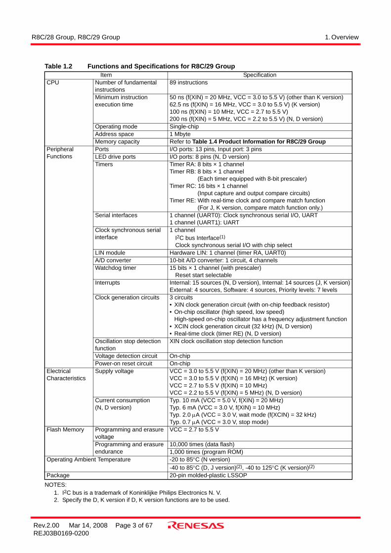
1.2 Performance Overview Table 1.1 outlines the Functions and Specifications for R8C/28 Group and Table 1.2 outlines the Functions andSpecifications for R8C/29 Group.
NOTES:1. I2C bus is a trademark of Koninklijke Philips Electronics N. V.2. Specify the D, K version if D, K version functions are to be used.
Table 1.1 Functions and Specifications for R8C/28 GroupItem Specification
CPU Number of fundamental instructions
89 instructions
Minimum instruction execution time
50 ns (f(XIN) = 20 MHz, VCC = 3.0 to 5.5 V) (other than K version)62.5 ns (f(XIN) = 16 MHz, VCC = 3.0 to 5.5 V) (K version)100 ns (f(XIN) = 10 MHz, VCC = 2.7 to 5.5 V)200 ns (f(XIN) = 5 MHz, VCC = 2.2 to 5.5 V) (N, D version)
Operating mode Single-chipAddress space 1 MbyteMemory capacity Refer to Table 1.3 Product Information for R8C/28 Group
Peripheral Functions
Ports I/O ports: 13 pins, Input port: 3 pinsLED drive ports I/O ports: 8 pins (N, D version)Timers Timer RA: 8 bits × 1 channel
Timer RB: 8 bits × 1 channel(Each timer equipped with 8-bit prescaler)
Timer RC: 16 bits × 1 channel(Input capture and output compare circuits)
Timer RE: With real-time clock and compare match function(For J, K version, compare match function only.)
Serial interfaces 1 channel (UART0): Clock synchronous serial I/O, UART1 channel (UART1): UART
Clock synchronous serial interface
1 channel I2C bus Interface(1)
Clock synchronous serial I/O with chip selectLIN module Hardware LIN: 1 channel (timer RA, UART0)A/D converter 10-bit A/D converter: 1 circuit, 4 channelsWatchdog timer 15 bits × 1 channel (with prescaler)
Reset start selectableInterrupts Internal: 15 sources (N, D version), Internal: 14 sources (J, K version)
External: 4 sources, Software: 4 sources, Priority levels: 7 levelsClock generation circuits 3 circuits
• XIN clock generation circuit (with on-chip feedback resistor)• On-chip oscillator (high speed, low speed)
High-speed on-chip oscillator has a frequency adjustment function• XCIN clock generation circuit (32 kHz) (N, D version)• Real-time clock (timer RE) (N, D version)
Oscillation stop detection function
XIN clock oscillation stop detection function
Voltage detection circuit On-chipPower-on reset circuit On-chip
Electrical Characteristics
Supply voltage VCC = 3.0 to 5.5 V (f(XIN) = 20 MHz) (other than K version)VCC = 3.0 to 5.5 V (f(XIN) = 16 MHz) (K version)VCC = 2.7 to 5.5 V (f(XIN) = 10 MHz)VCC = 2.2 to 5.5 V (f(XIN) = 5 MHz) (N, D version)
Current consumption (N, D version)
Typ. 10 mA (VCC = 5.0 V, f(XIN) = 20 MHz)Typ. 6 mA (VCC = 3.0 V, f(XIN) = 10 MHz)Typ. 2.0 µA (VCC = 3.0 V, wait mode (f(XCIN) = 32 kHz)Typ. 0.7 µA (VCC = 3.0 V, stop mode)
Flash Memory Programming and erasure voltage
VCC = 2.7 to 5.5 V
Programming and erasure endurance
100 times
Operating Ambient Temperature -20 to 85°C (N version)-40 to 85°C (D, J version)(2), -40 to 125°C (K version)(2)
Package 20-pin molded-plastic LSSOP
R8C/28 Group, R8C/29 Group 1. Overview
Rev.2.00 Mar 14, 2008 Page 3 of 67REJ03B0169-0200
NOTES:1. I2C bus is a trademark of Koninklijke Philips Electronics N. V.2. Specify the D, K version if D, K version functions are to be used.
Table 1.2 Functions and Specifications for R8C/29 GroupItem Specification
CPU Number of fundamental instructions
89 instructions
Minimum instruction execution time
50 ns (f(XIN) = 20 MHz, VCC = 3.0 to 5.5 V) (other than K version)62.5 ns (f(XIN) = 16 MHz, VCC = 3.0 to 5.5 V) (K version)100 ns (f(XIN) = 10 MHz, VCC = 2.7 to 5.5 V)200 ns (f(XIN) = 5 MHz, VCC = 2.2 to 5.5 V) (N, D version)
Operating mode Single-chipAddress space 1 MbyteMemory capacity Refer to Table 1.4 Product Information for R8C/29 Group
Peripheral Functions
Ports I/O ports: 13 pins, Input port: 3 pinsLED drive ports I/O ports: 8 pins (N, D version)Timers Timer RA: 8 bits × 1 channel
Timer RB: 8 bits × 1 channel (Each timer equipped with 8-bit prescaler)
Timer RC: 16 bits × 1 channel(Input capture and output compare circuits)
Timer RE: With real-time clock and compare match function(For J, K version, compare match function only.)
Serial interfaces 1 channel (UART0): Clock synchronous serial I/O, UART1 channel (UART1): UART
Clock synchronous serial interface
1 channel I2C bus Interface(1)
Clock synchronous serial I/O with chip selectLIN module Hardware LIN: 1 channel (timer RA, UART0)A/D converter 10-bit A/D converter: 1 circuit, 4 channelsWatchdog timer 15 bits × 1 channel (with prescaler)
Reset start selectableInterrupts Internal: 15 sources (N, D version), Internal: 14 sources (J, K version)
External: 4 sources, Software: 4 sources, Priority levels: 7 levelsClock generation circuits 3 circuits
• XIN clock generation circuit (with on-chip feedback resistor)• On-chip oscillator (high speed, low speed)
High-speed on-chip oscillator has a frequency adjustment function• XCIN clock generation circuit (32 kHz) (N, D version)• Real-time clock (timer RE) (N, D version)
Oscillation stop detection function
XIN clock oscillation stop detection function
Voltage detection circuit On-chipPower-on reset circuit On-chip
Electrical Characteristics
Supply voltage VCC = 3.0 to 5.5 V (f(XIN) = 20 MHz) (other than K version)VCC = 3.0 to 5.5 V (f(XIN) = 16 MHz) (K version)VCC = 2.7 to 5.5 V (f(XIN) = 10 MHz)VCC = 2.2 to 5.5 V (f(XIN) = 5 MHz) (N, D version)
Current consumption (N, D version)
Typ. 10 mA (VCC = 5.0 V, f(XIN) = 20 MHz)Typ. 6 mA (VCC = 3.0 V, f(XIN) = 10 MHz)Typ. 2.0 µA (VCC = 3.0 V, wait mode (f(XCIN) = 32 kHz)Typ. 0.7 µA (VCC = 3.0 V, stop mode)
Flash Memory Programming and erasure voltage
VCC = 2.7 to 5.5 V
Programming and erasure endurance
10,000 times (data flash)1,000 times (program ROM)
Operating Ambient Temperature -20 to 85°C (N version)-40 to 85°C (D, J version)(2), -40 to 125°C (K version)(2)
20-pin molded-plastic LSSOPPackage
R8C/28 Group, R8C/29 Group 1. Overview
Rev.2.00 Mar 14, 2008 Page 4 of 67REJ03B0169-0200
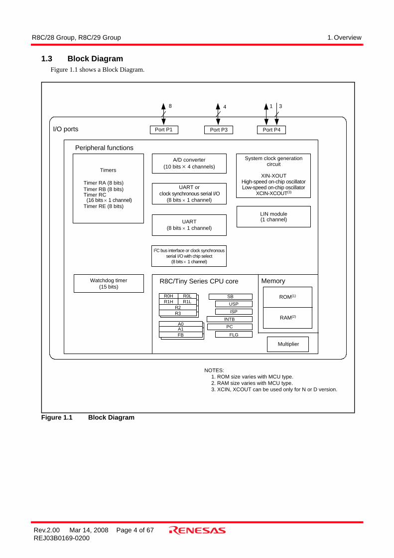
1.3 Block DiagramFigure 1.1 shows a Block Diagram.
Figure 1.1 Block Diagram
R8C/Tiny Series CPU core
System clock generationcircuit
XIN-XOUTHigh-speed on-chip oscillatorLow-speed on-chip oscillator
XCIN-XCOUT(3)
MemoryWatchdog timer(15 bits)
ROM(1)
RAM(2)
Multiplier
R0H R0LR1H
R2R3
R1L
A0A1FB
SBUSPISP
INTBPC
FLG
I/O ports
NOTES:1. ROM size varies with MCU type.2. RAM size varies with MCU type.3. XCIN, XCOUT can be used only for N or D version.
Timers
Timer RA (8 bits)Timer RB (8 bits)Timer RC (16 bits × 1 channel)Timer RE (8 bits)
A/D converter(10 bits × 4 channels)
UART orclock synchronous serial I/O
(8 bits × 1 channel)
I2C bus interface or clock synchronousserial I/O with chip select
(8 bits × 1 channel)
LIN module(1 channel)
8
Port P1
4
Port P3
1 3
Port P4
Peripheral functions
UART(8 bits × 1 channel)
R8C/28 Group, R8C/29 Group 1. Overview
Rev.2.00 Mar 14, 2008 Page 5 of 67REJ03B0169-0200
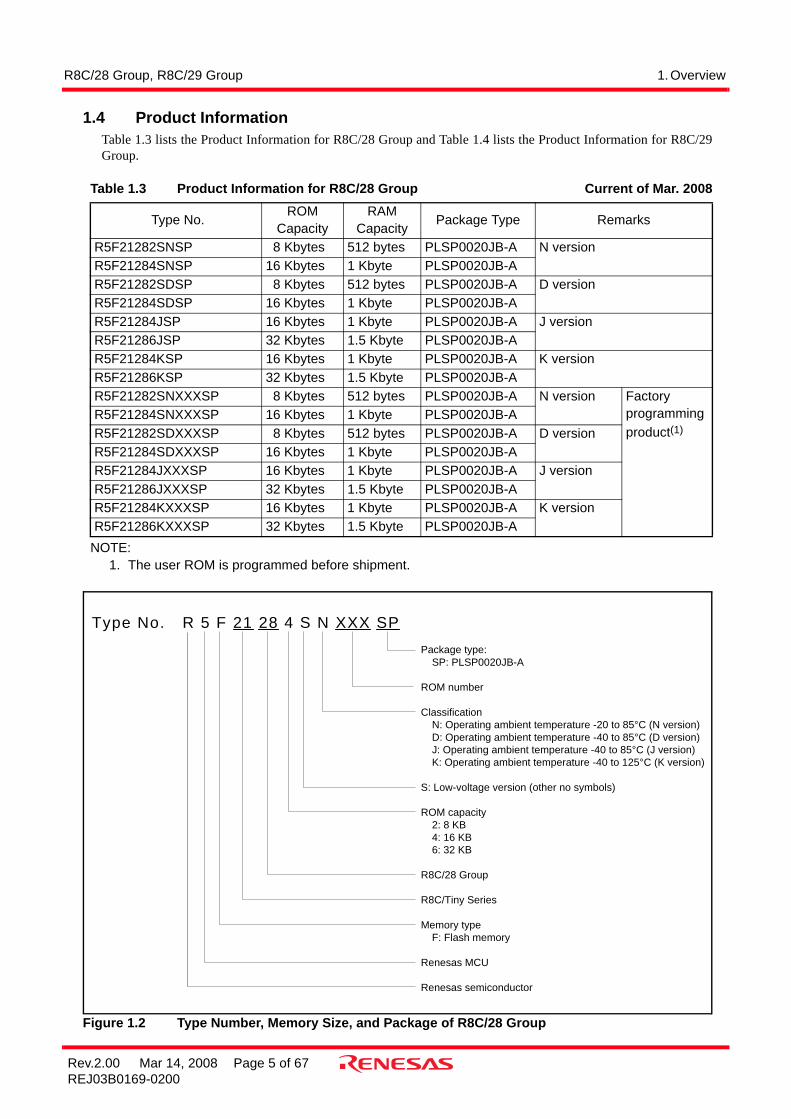
1.4 Product InformationTable 1.3 lists the Product Information for R8C/28 Group and Table 1.4 lists the Product Information for R8C/29Group.
NOTE:1. The user ROM is programmed before shipment.
Figure 1.2 Type Number, Memory Size, and Package of R8C/28 Group
Table 1.3 Product Information for R8C/28 Group Current of Mar. 2008
Type No. ROM Capacity
RAM Capacity Package Type Remarks
R5F21282SNSP 8 Kbytes 512 bytes PLSP0020JB-A N versionR5F21284SNSP 16 Kbytes 1 Kbyte PLSP0020JB-AR5F21282SDSP 8 Kbytes 512 bytes PLSP0020JB-A D versionR5F21284SDSP 16 Kbytes 1 Kbyte PLSP0020JB-AR5F21284JSP 16 Kbytes 1 Kbyte PLSP0020JB-A J versionR5F21286JSP 32 Kbytes 1.5 Kbyte PLSP0020JB-AR5F21284KSP 16 Kbytes 1 Kbyte PLSP0020JB-A K versionR5F21286KSP 32 Kbytes 1.5 Kbyte PLSP0020JB-AR5F21282SNXXXSP 8 Kbytes 512 bytes PLSP0020JB-A N version Factory
programming product(1)
R5F21284SNXXXSP 16 Kbytes 1 Kbyte PLSP0020JB-AR5F21282SDXXXSP 8 Kbytes 512 bytes PLSP0020JB-A D versionR5F21284SDXXXSP 16 Kbytes 1 Kbyte PLSP0020JB-AR5F21284JXXXSP 16 Kbytes 1 Kbyte PLSP0020JB-A J versionR5F21286JXXXSP 32 Kbytes 1.5 Kbyte PLSP0020JB-AR5F21284KXXXSP 16 Kbytes 1 Kbyte PLSP0020JB-A K versionR5F21286KXXXSP 32 Kbytes 1.5 Kbyte PLSP0020JB-A
Type No. R 5 F 21 28 4 S N XXX SPPackage type:
SP: PLSP0020JB-A
ROM number
ClassificationN: Operating ambient temperature -20 to 85°C (N version)D: Operating ambient temperature -40 to 85°C (D version)J: Operating ambient temperature -40 to 85°C (J version)K: Operating ambient temperature -40 to 125°C (K version)
S: Low-voltage version (other no symbols)
ROM capacity2: 8 KB4: 16 KB6: 32 KB
R8C/28 Group
R8C/Tiny Series
Memory typeF: Flash memory
Renesas MCU
Renesas semiconductor

R8C/28 Group, R8C/29 Group 1. Overview
Rev.2.00 Mar 14, 2008 Page 6 of 67REJ03B0169-0200
NOTE:1. The user ROM is programmed before shipment.
Figure 1.3 Type Number, Memory Size, and Package of R8C/29 Group
Table 1.4 Product Information for R8C/29 Group Current of Mar. 2008
Type No.ROM Capacity
RAM Capacity Package Type RemarksProgram
ROM Data flash
R5F21292SNSP 8 Kbytes 1 Kbyte × 2 512 bytes PLSP0020JB-A N versionR5F21294SNSP 16 Kbytes 1 Kbyte × 2 1 Kbyte PLSP0020JB-AR5F21292SDSP 8 Kbytes 1 Kbyte × 2 512 bytes PLSP0020JB-A D versionR5F21294SDSP 16 Kbytes 1 Kbyte × 2 1 Kbyte PLSP0020JB-AR5F21294JSP 16 Kbytes 1 Kbyte × 2 1 Kbyte PLSP0020JB-A J versionR5F21296JSP 32 Kbytes 1 Kbyte × 2 1.5 Kbyte PLSP0020JB-AR5F21294KSP 16 Kbytes 1 Kbyte × 2 1 Kbyte PLSP0020JB-A K versionR5F21296KSP 32 Kbytes 1 Kbyte × 2 1.5 Kbyte PLSP0020JB-AR5F21292SNXXXSP 8 Kbytes 1 Kbyte × 2 512 bytes PLSP0020JB-A N version Factory
programming product(1)
R5F21294SNXXXSP 16 Kbytes 1 Kbyte × 2 1 Kbyte PLSP0020JB-AR5F21292SDXXXSP 8 Kbytes 1 Kbyte × 2 512 bytes PLSP0020JB-A D versionR5F21294SDXXXSP 16 Kbytes 1 Kbyte × 2 1 Kbyte PLSP0020JB-AR5F21294JXXXSP 16 Kbytes 1 Kbyte × 2 1 Kbyte PLSP0020JB-A J versionR5F21296JXXXSP 32 Kbytes 1 Kbyte × 2 1.5 Kbyte PLSP0020JB-AR5F21294KXXXSP 16 Kbytes 1 Kbyte × 2 1 Kbyte PLSP0020JB-A K versionR5F21296KXXXSP 32 Kbytes 1 Kbyte × 2 1.5 Kbyte PLSP0020JB-A
Type No. R 5 F 21 29 4 S N XXX SPPackage type:
SP: PLSP0020JB-A
ROM number
ClassificationN: Operating ambient temperature -20 to 85°C (N version)D: Operating ambient temperature -40 to 85°C (D version)J: Operating ambient temperature -40 to 85°C (J version)K: Operating ambient temperature -40 to 125°C (K version)
S: Low-voltage version (other no symbols)
ROM capacity2: 8 KB4: 16 KB6: 32 KB
R8C/29 Group
R8C/Tiny Series
Memory typeF: Flash memory
Renesas MCU
Renesas semiconductor

R8C/28 Group, R8C/29 Group 1. Overview
Rev.2.00 Mar 14, 2008 Page 7 of 67REJ03B0169-0200
1.5 Pin AssignmentsFigure 1.4 shows Pin Assignments (Top View).
Figure 1.4 Pin Assignments (Top View)
NOTES:1. P4_7 is an input-only port.2. Can be assigned to the pin in parentheses by a program.3. XCIN, XCOUT can be used only for N or D version.4. Confirm the pin 1 position on the package by referring to the package dimensions.
1
2
3
4
5
6
7
8
9
10
20 P3_4/SDA/SCS/TRCIOC
19 P3_3/INT3/SSI/TRCCLK
18 P1_0/KI0/AN8
17 P1_1/KI1/AN9/TRCIOA/TRCTRG
16 VREF/P4_2
15 P1_2/KI2/AN10/TRCIOB
14 P1_3/KI3/AN11/TRBO
13 P1_4/TXD0
12 P1_5/RXD0/(TRAIO)/(INT1)(2)
11 P1_6/CLK0/(SSI)(2)
P3_5/SCL/SSCK/TRCIOD
P3_7/TRAO/SSO/RXD1/(TXD1)(2)
RESET
XOUT/XCOUT/P4_7(1, 3)
VSS/AVSS
XIN/XCIN/P4_6(3)
VCC/AVCC
MODE
P4_5/INT0/(RXD1)(2)
P1_7/TRAIO/INT1
R8C
/28 Group
R8C
/29 Group
PLS
P0020JB
-A(20P
2F-A)
(top view)
R8C/28 Group, R8C/29 Group 1. Overview
Rev.2.00 Mar 14, 2008 Page 8 of 67REJ03B0169-0200
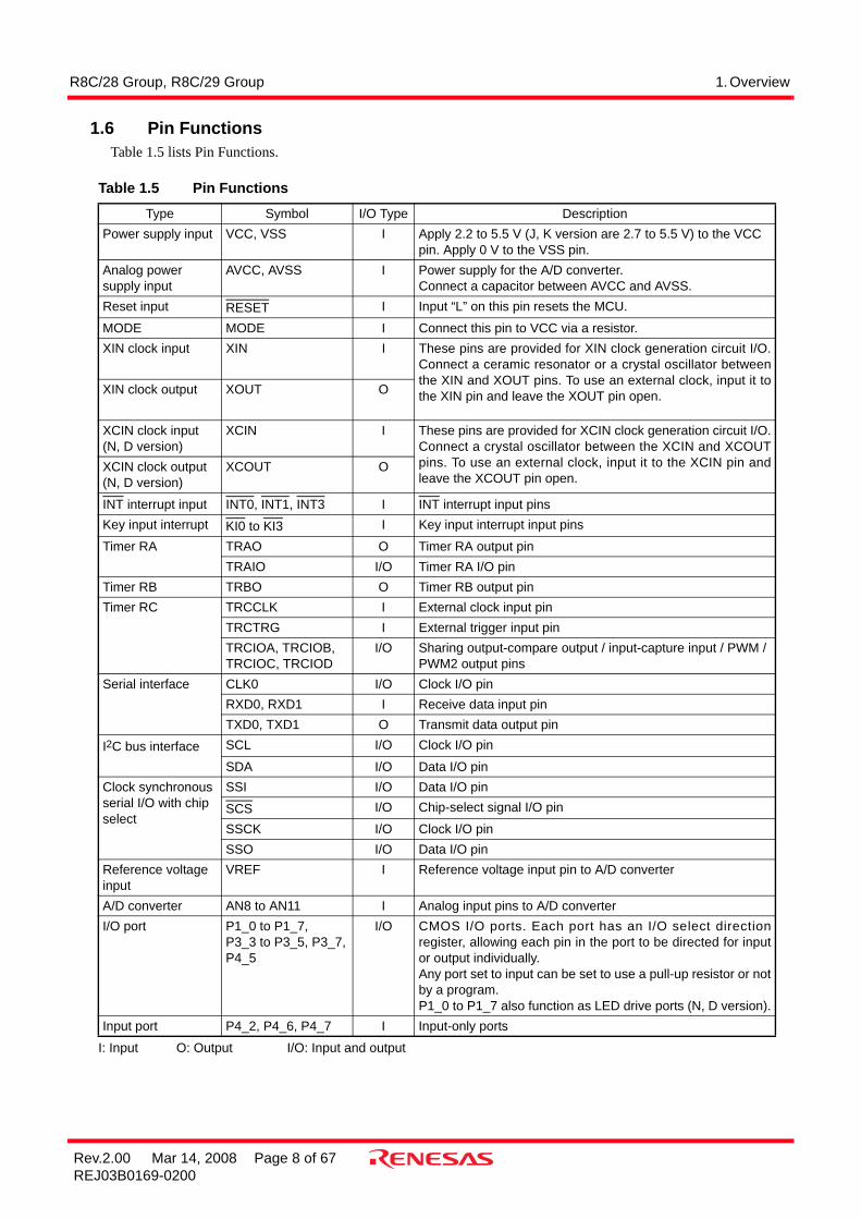
1.6 Pin FunctionsTable 1.5 lists Pin Functions.
I: Input O: Output I/O: Input and output
Table 1.5 Pin Functions
Type Symbol I/O Type DescriptionPower supply input VCC, VSS I Apply 2.2 to 5.5 V (J, K version are 2.7 to 5.5 V) to the VCC
pin. Apply 0 V to the VSS pin.Analog power supply input
AVCC, AVSS I Power supply for the A/D converter.Connect a capacitor between AVCC and AVSS.
Reset input RESET I Input “L” on this pin resets the MCU.
MODE MODE I Connect this pin to VCC via a resistor.XIN clock input XIN I These pins are provided for XIN clock generation circuit I/O.
Connect a ceramic resonator or a crystal oscillator betweenthe XIN and XOUT pins. To use an external clock, input it tothe XIN pin and leave the XOUT pin open.XIN clock output XOUT O
XCIN clock input(N, D version)
XCIN I These pins are provided for XCIN clock generation circuit I/O.Connect a crystal oscillator between the XCIN and XCOUTpins. To use an external clock, input it to the XCIN pin andleave the XCOUT pin open.
XCIN clock output(N, D version)
XCOUT O
INT interrupt input INT0, INT1, INT3 I INT interrupt input pinsKey input interrupt KI0 to KI3 I Key input interrupt input pins
Timer RA TRAO O Timer RA output pinTRAIO I/O Timer RA I/O pin
Timer RB TRBO O Timer RB output pinTimer RC TRCCLK I External clock input pin
TRCTRG I External trigger input pinTRCIOA, TRCIOB, TRCIOC, TRCIOD
I/O Sharing output-compare output / input-capture input / PWM / PWM2 output pins
Serial interface CLK0 I/O Clock I/O pinRXD0, RXD1 I Receive data input pinTXD0, TXD1 O Transmit data output pin
I2C bus interface SCL I/O Clock I/O pin
SDA I/O Data I/O pinClock synchronous serial I/O with chip select
SSI I/O Data I/O pin
SCS I/O Chip-select signal I/O pin
SSCK I/O Clock I/O pinSSO I/O Data I/O pin
Reference voltage input
VREF I Reference voltage input pin to A/D converter
A/D converter AN8 to AN11 I Analog input pins to A/D converterI/O port P1_0 to P1_7,
P3_3 to P3_5, P3_7,P4_5
I/O CMOS I/O ports. Each port has an I/O select directionregister, allowing each pin in the port to be directed for inputor output individually.Any port set to input can be set to use a pull-up resistor or notby a program.P1_0 to P1_7 also function as LED drive ports (N, D version).
Input port P4_2, P4_6, P4_7 I Input-only ports
R8C/28 Group, R8C/29 Group 1. Overview
Rev.2.00 Mar 14, 2008 Page 9 of 67REJ03B0169-0200
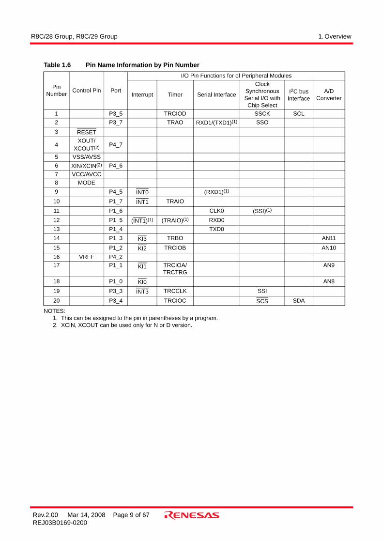
NOTES:1. This can be assigned to the pin in parentheses by a program.2. XCIN, XCOUT can be used only for N or D version.
Table 1.6 Pin Name Information by Pin Number
Pin Number Control Pin Port
I/O Pin Functions for of Peripheral Modules
Interrupt Timer Serial Interface
Clock Synchronous Serial I/O with Chip Select
I2C bus Interface
A/D Converter
1 P3_5 TRCIOD SSCK SCL2 P3_7 TRAO RXD1/(TXD1)(1) SSO3 RESET
4XOUT/
XCOUT(2) P4_7
5 VSS/AVSS6 XIN/XCIN(2) P4_67 VCC/AVCC8 MODE9 P4_5 INT0 (RXD1)(1)
10 P1_7 INT1 TRAIO11 P1_6 CLK0 (SSI)(1)
12 P1_5 (INT1)(1) (TRAIO)(1) RXD013 P1_4 TXD014 P1_3 KI3 TRBO AN11
15 P1_2 KI2 TRCIOB AN1016 VRFF P4_217 P1_1 KI1 TRCIOA/
TRCTRGAN9
18 P1_0 KI0 AN8
19 P3_3 INT3 TRCCLK SSI
20 P3_4 TRCIOC SCS SDA

R8C/28 Group, R8C/29 Group 2. Central Processing Unit (CPU)
Rev.2.00 Mar 14, 2008 Page 10 of 67REJ03B0169-0200
2. Central Processing Unit (CPU)Figure 2.1 shows the CPU Registers. The CPU contains 13 registers. R0, R1, R2, R3, A0, A1, and FB configure aregister bank. There are two sets of register bank.
Figure 2.1 CPU Registers
R2b31 b15 b8b7 b0
Data registers(1)
Address registers(1)
R3R0H (high-order of R0)
R2R3A0A1
INTBHb15b19 b0
INTBL
FB Frame base register(1)
The 4 high order bits of INTB are INTBH andthe 16 low order bits of INTB are INTBL.
Interrupt table register
b19 b0
USP
Program counter
ISPSB
User stack pointer
Interrupt stack pointer
Static base register
PC
FLG Flag register
Carry flagDebug flagZero flagSign flagRegister bank select flagOverflow flagInterrupt enable flagStack pointer select flagReserved bitProcessor interrupt priority levelReserved bit
CIPL DZSBOIU
b15 b0
b15 b0
b15 b0b8 b7
NOTE:1. These registers comprise a register bank. There are two register banks.
R1H (high-order of R1)
R0L (low-order of R0)
R1L (low-order of R1)
R8C/28 Group, R8C/29 Group 2. Central Processing Unit (CPU)
Rev.2.00 Mar 14, 2008 Page 11 of 67REJ03B0169-0200
2.1 Data Registers (R0, R1, R2, and R3)R0 is a 16-bit register for transfer, arithmetic, and logic operations. The same applies to R1 to R3. R0 can be splitinto high-order bits (R0H) and low-order bits (R0L) to be used separately as 8-bit data registers. R1H and R1L areanalogous to R0H and R0L. R2 can be combined with R0 and used as a 32-bit data register (R2R0). R3R1 isanalogous to R2R0.
2.2 Address Registers (A0 and A1)A0 is a 16-bit register for address register indirect addressing and address register relative addressing. It is alsoused for transfer, arithmetic, and logic operations. A1 is analogous to A0. A1 can be combined with A0 and as a 32-bit address register (A1A0).
2.3 Frame Base Register (FB)FB is a 16-bit register for FB relative addressing.
2.4 Interrupt Table Register (INTB)INTB is a 20-bit register that indicates the start address of an interrupt vector table.
2.5 Program Counter (PC)PC is 20 bits wide and indicates the address of the next instruction to be executed.
2.6 User Stack Pointer (USP) and Interrupt Stack Pointer (ISP)The stack pointers (SP), USP, and ISP, are each 16 bits wide. The U flag of FLG is used to switch betweenUSP and ISP.
2.7 Static Base Register (SB)SB is a 16-bit register for SB relative addressing.
2.8 Flag Register (FLG)FLG is an 11-bit register indicating the CPU state.
2.8.1 Carry Flag (C)The C flag retains carry, borrow, or shift-out bits that have been generated by the arithmetic and logic unit.
2.8.2 Debug Flag (D)The D flag is for debugging only. Set it to 0.
2.8.3 Zero Flag (Z)The Z flag is set to 1 when an arithmetic operation results in 0; otherwise to 0.
2.8.4 Sign Flag (S)The S flag is set to 1 when an arithmetic operation results in a negative value; otherwise to 0.
2.8.5 Register Bank Select Flag (B)Register bank 0 is selected when the B flag is 0. Register bank 1 is selected when this flag is set to 1.
2.8.6 Overflow Flag (O)The O flag is set to 1 when an operation results in an overflow; otherwise to 0.

R8C/28 Group, R8C/29 Group 2. Central Processing Unit (CPU)
Rev.2.00 Mar 14, 2008 Page 12 of 67REJ03B0169-0200
2.8.7 Interrupt Enable Flag (I)The I flag enables maskable interrupts.Interrupt are disabled when the I flag is set to 0, and are enabled when the I flag is set to 1. The I flag is set to 0when an interrupt request is acknowledged.
2.8.8 Stack Pointer Select Flag (U)ISP is selected when the U flag is set to 0; USP is selected when the U flag is set to 1.The U flag is set to 0 when a hardware interrupt request is acknowledged or the INT instruction of softwareinterrupt numbers 0 to 31 is executed.
2.8.9 Processor Interrupt Priority Level (IPL)IPL is 3 bits wide and assigns processor interrupt priority levels from level 0 to level 7.If a requested interrupt has higher priority than IPL, the interrupt is enabled.
2.8.10 Reserved BitIf necessary, set to 0. When read, the content is undefined.

R8C/28 Group, R8C/29 Group 3. Memory
Rev.2.00 Mar 14, 2008 Page 13 of 67REJ03B0169-0200
3. Memory
3.1 R8C/28 GroupFigure 3.1 is a Memory Map of R8C/28 Group. The R8C/28 group has 1 Mbyte of address space from addresses00000h to FFFFFh.The internal ROM is allocated lower addresses, beginning with address 0FFFFh. For example, a 16-Kbyte internalROM area is allocated addresses 0C000h to 0FFFFh.The fixed interrupt vector table is allocated addresses 0FFDCh to 0FFFFh. They store the starting address of eachinterrupt routine. The internal RAM is allocated higher addresses, beginning with address 00400h. For example, a 1-Kbyte internalRAM area is allocated addresses 00400h to 007FFh. The internal RAM is used not only for storing data but also forcalling subroutines and as stacks when interrupt requests are acknowledged.Special function registers (SFRs) are allocated addresses 00000h to 002FFh. The peripheral function controlregisters are allocated here. All addresses within the SFR, which have nothing allocated are reserved for future useand cannot be accessed by users.
Figure 3.1 Memory Map of R8C/28 Group
Undefined instructionOverflow
BRK instructionAddress match
Single stepWatchdog timer/oscillation stop detection/voltage monitor
(Reserved)(Reserved)
Reset
00400h
002FFh
00000h
Internal RAM
SFR(Refer to 4. SpecialFunction Registers
(SFRs))
0FFFFh
0FFDCh
NOTE:1. The blank regions are reserved. Do not access locations in these regions.
FFFFFh
0FFFFh
0YYYYh
Internal ROM(program ROM)
0XXXh
Part NumberInternal ROM Internal RAM
Size Address 0YYYYh Size Address 0XXXXh
R5F21284SNSP, R5F21284SDSP,R5F21284JSP, R5F21284KSP,R5F21284SNXXXSP, R5F21284SDXXXSP,R5F21284JXXXSP, R5F21284KXXXSP
8 Kbytes
16 Kbytes
32 Kbytes
0E000h
0C000h
08000h
512 bytes
1 Kbyte
1.5 Kbytes
005FFh
007FFh
009FFh
R5F21282SNSP, R5F21282SDSP,R5F21282SNXXXSP, R5F21282SDXXXSP
R5F21286JSP, R5F21286KSP,R5F21286JXXXSP, R5F21286KXXXSP

R8C/28 Group, R8C/29 Group 3. Memory
Rev.2.00 Mar 14, 2008 Page 14 of 67REJ03B0169-0200
3.2 R8C/29 GroupFigure 3.2 is a Memory Map of R8C/29 Group. The R8C/29 group has 1 Mbyte of address space from addresses00000h to FFFFFh.The internal ROM (program ROM) is allocated lower addresses, beginning with address 0FFFFh. For example, a16-Kbyte internal ROM area is allocated addresses 0C000h to 0FFFFh.The fixed interrupt vector table is allocated addresses 0FFDCh to 0FFFFh. They store the starting address of eachinterrupt routine. The internal ROM (data flash) is allocated addresses 02400h to 02BFFh.The internal RAM area is allocated higher addresses, beginning with address 00400h. For example, a 1-Kbyteinternal RAM is allocated addresses 00400h to 007FFh. The internal RAM is used not only for storing data but alsofor calling subroutines and as stacks when interrupt requests are acknowledged.Special function registers (SFRs) are allocated addresses 00000h to 002FFh. The peripheral function controlregisters are allocated here. All addresses within the SFR, which have nothing allocated are reserved for future useand cannot be accessed by users.
Figure 3.2 Memory Map of R8C/29 Group
Undefined instructionOverflow
BRK instructionAddress match
Single stepWatchdog timer/oscillation stop detection/voltage monitor
(Reserved)(Reserved)
Reset
FFFFFh
0FFFFh
0YYYYh
00400h
002FFh
00000h
Internal ROM(program ROM)
Internal RAM
SFR(Refer to 4. SpecialFunction Registers
(SFRs))
0FFFFh
0FFDChInternal ROM(data flash)(1)
NOTES: 1. Data flash block A (1 Kbyte) and B (1 Kbyte) are shown. 2. The blank regions are reserved. Do not access locations in these regions.
0XXXXh
02400h
02BFFh
Part NumberInternal ROM Internal RAM
Size Address 0YYYYh Size Address 0XXXXh
8 Kbytes
16 Kbytes
32 Kbytes
0E000h
0C000h
08000h
512 bytes
1 Kbyte
1.5 Kbytes
005FFh
007FFh
009FFh
R5F21294SNSP, R5F21294SDSP,R5F21294JSP, R5F21294KSP,R5F21294SNXXXSP, R5F21294SDXXXSP,R5F21294JXXXSP, R5F21294KXXXSP
R5F21292SNSP, R5F21292SDSP,R5F21292SNXXXSP, R5F21292SDXXXSP
R5F21296JSP, R5F21296KSP,R5F21296JXXXSP, R5F21296KXXXSP

R8C/28 Group, R8C/29 Group 4. Special Function Registers (SFRs)
Rev.2.00 Mar 14, 2008 Page 15 of 67REJ03B0169-0200
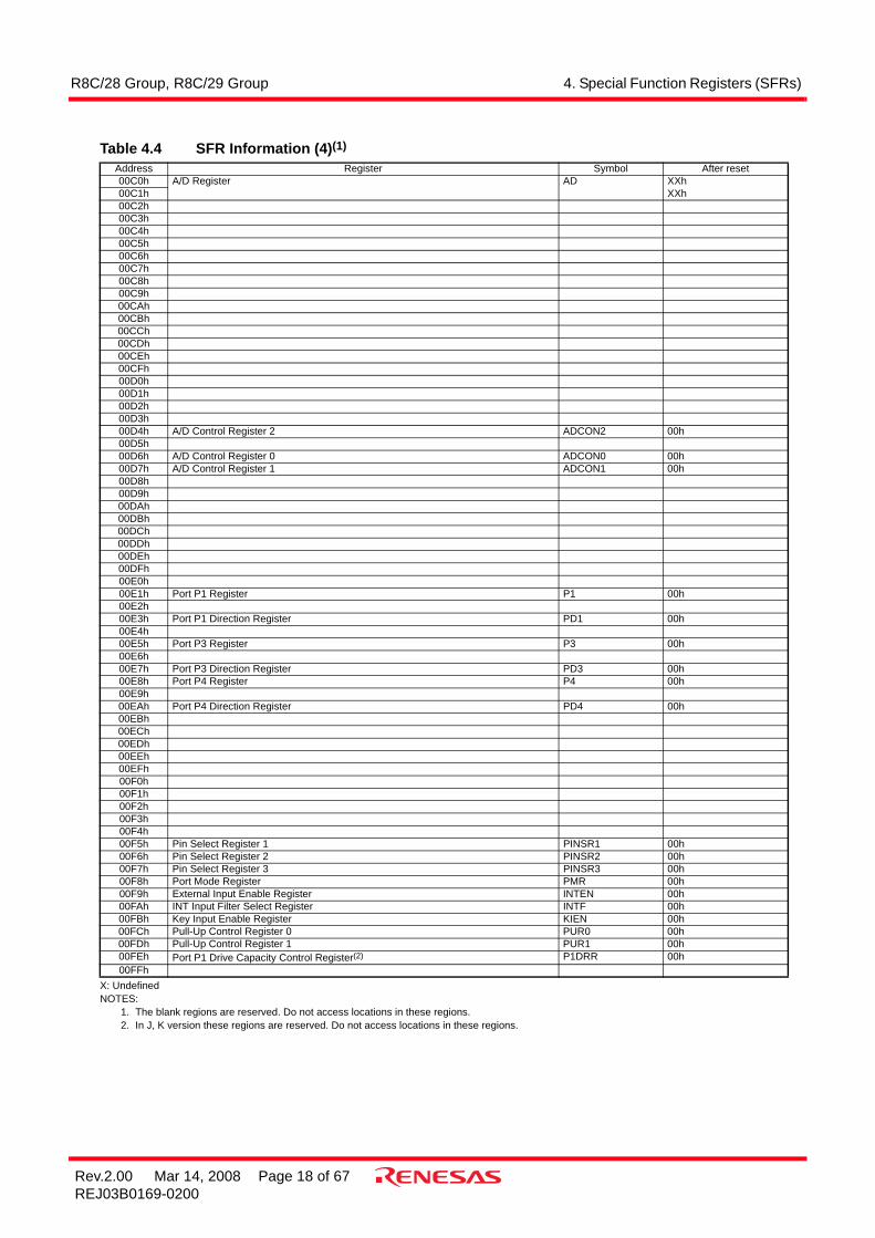
4. Special Function Registers (SFRs)An SFR (special function register) is a control register for a peripheral function. Tables 4.1 to 4.7 list the specialfunction registers.
Table 4.1 SFR Information (1)(1)
X: UndefinedNOTES:
1. The blank regions are reserved. Do not access locations in these regions. 2. The CSPROINI bit in the OFS register is set to 0.3. In J, K version these regions are reserved. Do not access locations in these regions.
Address Register Symbol After reset0000h0001h0002h0003h0004h Processor Mode Register 0 PM0 00h0005h Processor Mode Register 1 PM1 00h0006h System Clock Control Register 0 CM0 01101000b0007h System Clock Control Register 1 CM1 00100000b0008h0009h000Ah Protect Register PRCR 00h000Bh000Ch Oscillation Stop Detection Register OCD 00000100b000Dh Watchdog Timer Reset Register WDTR XXh000Eh Watchdog Timer Start Register WDTS XXh000Fh Watchdog Timer Control Register WDC 00X11111b0010h Address Match Interrupt Register 0 RMAD0 00h0011h 00h0012h 00h0013h Address Match Interrupt Enable Register AIER 00h0014h Address Match Interrupt Register 1 RMAD1 00h0015h 00h0016h 00h0017h0018h0019h001Ah001Bh001Ch Count Source Protection Mode Register CSPR 00h
10000000b(2)
001Dh001Eh001Fh0020h0021h0022h0023h High-Speed On-Chip Oscillator Control Register 0 FRA0 00h0024h High-Speed On-Chip Oscillator Control Register 1 FRA1 When shipping0025h High-Speed On-Chip Oscillator Control Register 2 FRA2 00h0026h0027h0028h Clock Prescaler Reset Flag CPSRF 00h0029h High-Speed On-Chip Oscillator Control Register 4(3) FRA4 When shipping002Ah002Bh High-Speed On-Chip Oscillator Control Register 6(3) FRA6 When shipping002Ch High-Speed On-Chip Oscillator Control Register 7(3) FRA7 When shipping002Dh002Eh002Fh
R8C/28 Group, R8C/29 Group 4. Special Function Registers (SFRs)
Rev.2.00 Mar 14, 2008 Page 16 of 67REJ03B0169-0200
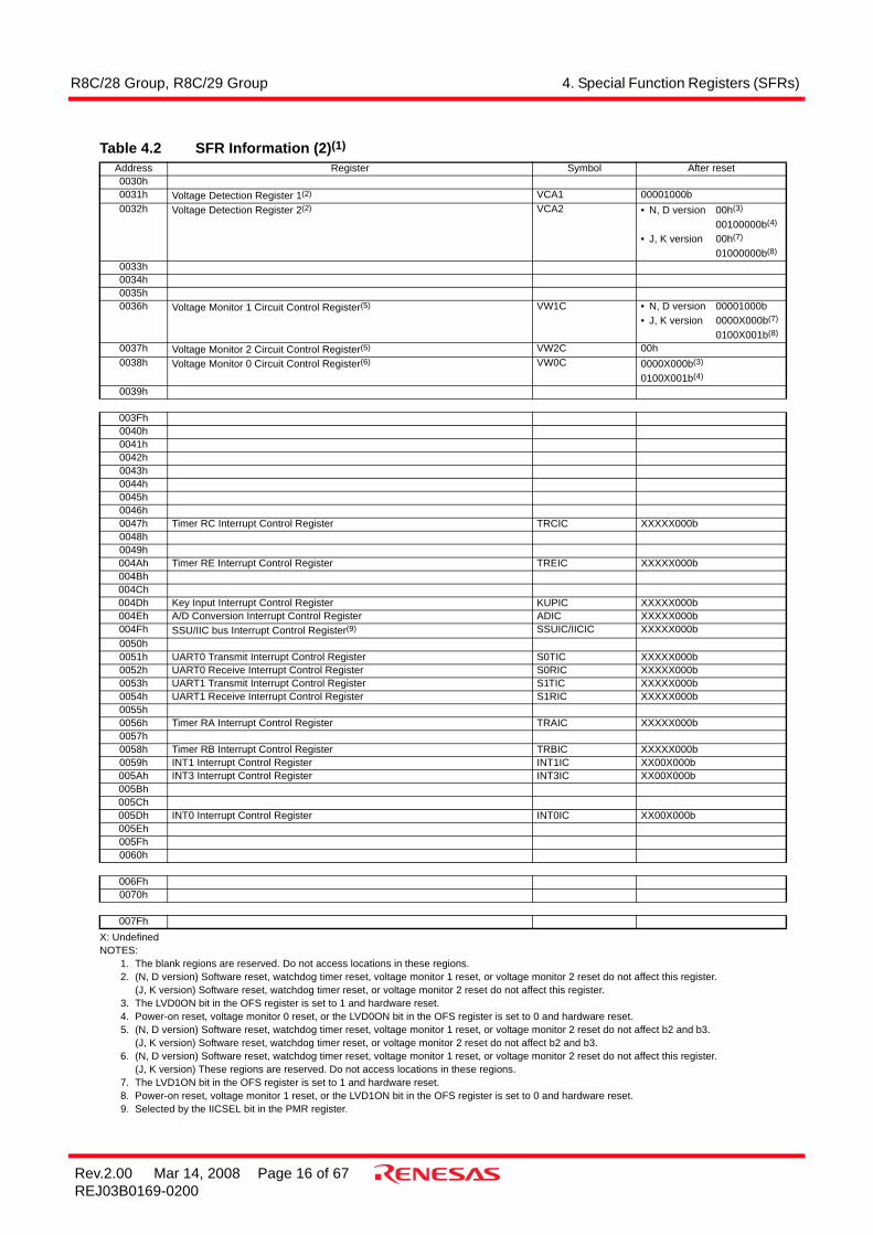
Table 4.2 SFR Information (2)(1)
X: UndefinedNOTES:
1. The blank regions are reserved. Do not access locations in these regions.2. (N, D version) Software reset, watchdog timer reset, voltage monitor 1 reset, or voltage monitor 2 reset do not affect this register.
(J, K version) Software reset, watchdog timer reset, or voltage monitor 2 reset do not affect this register.3. The LVD0ON bit in the OFS register is set to 1 and hardware reset.4. Power-on reset, voltage monitor 0 reset, or the LVD0ON bit in the OFS register is set to 0 and hardware reset.5. (N, D version) Software reset, watchdog timer reset, voltage monitor 1 reset, or voltage monitor 2 reset do not affect b2 and b3.
(J, K version) Software reset, watchdog timer reset, or voltage monitor 2 reset do not affect b2 and b3.6. (N, D version) Software reset, watchdog timer reset, voltage monitor 1 reset, or voltage monitor 2 reset do not affect this register.
(J, K version) These regions are reserved. Do not access locations in these regions.7. The LVD1ON bit in the OFS register is set to 1 and hardware reset.8. Power-on reset, voltage monitor 1 reset, or the LVD1ON bit in the OFS register is set to 0 and hardware reset.9. Selected by the IICSEL bit in the PMR register.
Address Register Symbol After reset0030h0031h Voltage Detection Register 1(2) VCA1 00001000b0032h Voltage Detection Register 2(2) VCA2 • N, D version 00h(3)
00100000b(4)
• J, K version 00h(7)
01000000b(8)
0033h0034h0035h0036h Voltage Monitor 1 Circuit Control Register(5) VW1C • N, D version 00001000b
• J, K version 0000X000b(7)
0100X001b(8)
0037h Voltage Monitor 2 Circuit Control Register(5) VW2C 00h0038h Voltage Monitor 0 Circuit Control Register(6) VW0C 0000X000b(3)
0100X001b(4)
0039h
003Fh0040h0041h0042h0043h0044h0045h0046h0047h Timer RC Interrupt Control Register TRCIC XXXXX000b0048h0049h004Ah Timer RE Interrupt Control Register TREIC XXXXX000b004Bh004Ch004Dh Key Input Interrupt Control Register KUPIC XXXXX000b004Eh A/D Conversion Interrupt Control Register ADIC XXXXX000b004Fh SSU/IIC bus Interrupt Control Register(9) SSUIC/IICIC XXXXX000b0050h0051h UART0 Transmit Interrupt Control Register S0TIC XXXXX000b0052h UART0 Receive Interrupt Control Register S0RIC XXXXX000b0053h UART1 Transmit Interrupt Control Register S1TIC XXXXX000b0054h UART1 Receive Interrupt Control Register S1RIC XXXXX000b0055h0056h Timer RA Interrupt Control Register TRAIC XXXXX000b0057h0058h Timer RB Interrupt Control Register TRBIC XXXXX000b0059h INT1 Interrupt Control Register INT1IC XX00X000b005Ah INT3 Interrupt Control Register INT3IC XX00X000b005Bh005Ch005Dh INT0 Interrupt Control Register INT0IC XX00X000b005Eh005Fh0060h
006Fh0070h
007Fh

R8C/28 Group, R8C/29 Group 4. Special Function Registers (SFRs)
Rev.2.00 Mar 14, 2008 Page 17 of 67REJ03B0169-0200
Table 4.3 SFR Information (3)(1)
X: UndefinedNOTES:
1. The blank regions are reserved. Do not access locations in these regions.2. Selected by the IICSEL bit in the PMR register.
Address Register Symbol After reset0080h0081h0082h0083h0084h0085h0086h0087h0088h0089h008Ah008Bh008Ch008Dh008Eh008Fh0090h0091h0092h0093h0094h0095h0096h0097h0098h0099h009Ah009Bh009Ch009Dh009Eh009Fh00A0h UART0 Transmit/Receive Mode Register U0MR 00h00A1h UART0 Bit Rate Register U0BRG XXh00A2h UART0 Transmit Buffer Register U0TB XXh00A3h XXh00A4h UART0 Transmit/Receive Control Register 0 U0C0 00001000b00A5h UART0 Transmit/Receive Control Register 1 U0C1 00000010b00A6h UART0 Receive Buffer Register U0RB XXh00A7h XXh00A8h UART1 Transmit/Receive Mode Register U1MR 00h00A9h UART1 Bit Rate Register U1BRG XXh00AAh UART1 Transmit Buffer Register U1TB XXh00ABh XXh00ACh UART1 Transmit/Receive Control Register 0 U1C0 00001000b00ADh UART1 Transmit/Receive Control Register 1 U1C1 00000010b00AEh UART1 Receive Buffer Register U1RB XXh00AFh XXh00B0h00B1h00B2h00B3h00B4h00B5h00B6h00B7h00B8h SS Control Register H / IIC bus Control Register 1(2) SSCRH / ICCR1 00h00B9h SS Control Register L / IIC bus Control Register 2(2) SSCRL / ICCR2 01111101b00BAh SS Mode Register / IIC bus Mode Register(2) SSMR / ICMR 00011000b00BBh SS Enable Register / IIC bus Interrupt Enable Register(2) SSER / ICIER 00h00BCh SS Status Register / IIC bus Status Register(2) SSSR / ICSR 00h / 0000X000b00BDh SS Mode Register 2 / Slave Address Register(2) SSMR2 / SAR 00h00BEh SS Transmit Data Register / IIC bus Transmit Data Register(2) SSTDR / ICDRT FFh00BFh SS Receive Data Register / IIC bus Receive Data Register(2) SSRDR / ICDRR FFh
R8C/28 Group, R8C/29 Group 4. Special Function Registers (SFRs)
Rev.2.00 Mar 14, 2008 Page 18 of 67REJ03B0169-0200
Table 4.4 SFR Information (4)(1)
X: UndefinedNOTES:
1. The blank regions are reserved. Do not access locations in these regions.2. In J, K version these regions are reserved. Do not access locations in these regions.
Address Register Symbol After reset00C0h A/D Register AD XXh00C1h XXh00C2h00C3h00C4h00C5h00C6h00C7h00C8h00C9h00CAh00CBh00CCh00CDh00CEh00CFh00D0h00D1h00D2h00D3h00D4h A/D Control Register 2 ADCON2 00h00D5h00D6h A/D Control Register 0 ADCON0 00h00D7h A/D Control Register 1 ADCON1 00h00D8h00D9h00DAh00DBh00DCh00DDh00DEh00DFh00E0h00E1h Port P1 Register P1 00h00E2h00E3h Port P1 Direction Register PD1 00h00E4h00E5h Port P3 Register P3 00h00E6h00E7h Port P3 Direction Register PD3 00h00E8h Port P4 Register P4 00h00E9h00EAh Port P4 Direction Register PD4 00h00EBh00ECh00EDh00EEh00EFh00F0h00F1h00F2h00F3h00F4h00F5h Pin Select Register 1 PINSR1 00h00F6h Pin Select Register 2 PINSR2 00h00F7h Pin Select Register 3 PINSR3 00h00F8h Port Mode Register PMR 00h00F9h External Input Enable Register INTEN 00h00FAh INT Input Filter Select Register INTF 00h00FBh Key Input Enable Register KIEN 00h00FCh Pull-Up Control Register 0 PUR0 00h00FDh Pull-Up Control Register 1 PUR1 00h00FEh Port P1 Drive Capacity Control Register(2) P1DRR 00h00FFh

R8C/28 Group, R8C/29 Group 4. Special Function Registers (SFRs)
Rev.2.00 Mar 14, 2008 Page 19 of 67REJ03B0169-0200
Table 4.5 SFR Information (5)(1)
NOTES:1. The blank regions are reserved. Do not access locations in these regions.2. In J, K version these regions are reserved. Do not access locations in these regions.
Address Register Symbol After reset0100h Timer RA Control Register TRACR 00h0101h Timer RA I/O Control Register TRAIOC 00h0102h Timer RA Mode Register TRAMR 00h0103h Timer RA Prescaler Register TRAPRE FFh0104h Timer RA Register TRA FFh0105h0106h LIN Control Register LINCR 00h0107h LIN Status Register LINST 00h0108h Timer RB Control Register TRBCR 00h0109h Timer RB One-Shot Control Register TRBOCR 00h010Ah Timer RB I/O Control Register TRBIOC 00h010Bh Timer RB Mode Register TRBMR 00h010Ch Timer RB Prescaler Register TRBPRE FFh010Dh Timer RB Secondary Register TRBSC FFh010Eh Timer RB Primary Register TRBPR FFh010Fh0110h0111h0112h0113h0114h0115h0116h0117h0118h Timer RE Second Data Register / Counter Data Register TRESEC 00h0119h Timer RE Minute Data Register / Compare Data Register TREMIN 00h011Ah Timer RE Hour Data Register(2) TREHR 00h011Bh Timer RE Day of Week Data Register(2) TREWK 00h011Ch Timer RE Control Register 1 TRECR1 00h011Dh Timer RE Control Register 2 TRECR2 00h011Eh Timer RE Count Source Select Register TRECSR 00001000b011Fh0120h Timer RC Mode Register TRCMR 01001000b0121h Timer RC Control Register 1 TRCCR1 00h0122h Timer RC Interrupt Enable Register TRCIER 01110000b0123h Timer RC Status Register TRCSR 01110000b0124h Timer RC I/O Control Register 0 TRCIOR0 10001000b0125h Timer RC I/O Control Register 1 TRCIOR1 10001000b0126h Timer RC Counter TRC 00h0127h 00h0128h Timer RC General Register A TRCGRA FFh0129h FFh012Ah Timer RC General Register B TRCGRB FFh012Bh FFh012Ch Timer RC General Register C TRCGRC FFh012Dh FFh012Eh Timer RC General Register D TRCGRD FFh012Fh FFh0130h Timer RC Control Register 2 TRCCR2 00011111b0131h Timer RC Digital Filter Function Select Register TRCDF 00h0132h Timer RC Output Master Enable Register TRCOER 01111111b0133h0134h0135h0136h0137h0138h0139h013Ah013Bh013Ch013Dh013Eh013Fh

R8C/28 Group, R8C/29 Group 4. Special Function Registers (SFRs)
Rev.2.00 Mar 14, 2008 Page 20 of 67REJ03B0169-0200
Table 4.6 SFR Information (6)(1)
NOTE:1. The blank regions are reserved. Do not access locations in these regions.
Address Register Symbol After reset0140h0141h0142h0143h0144h0145h0146h0147h0148h0149h014Ah014Bh014Ch014Dh014Eh014Fh0150h0151h0152h0153h0154h0155h0156h0157h0158h0159h015Ah015Bh015Ch015Dh015Eh015Fh0160h0161h0162h0163h0164h0165h0166h0167h0168h0169h016Ah016Bh016Ch016Dh016Eh016Fh0170h0171h0172h0173h0174h0175h0176h0177h0178h0179h017Ah017Bh017Ch017Dh017Eh017Fh

R8C/28 Group, R8C/29 Group 4. Special Function Registers (SFRs)
Rev.2.00 Mar 14, 2008 Page 21 of 67REJ03B0169-0200
Table 4.7 SFR Information (7)(1)
X: UndefinedNOTES:
1. The blank regions are reserved. Do not access locations in these regions.2. The OFS register cannot be changed by a program. Use a flash programmer to write to it.
Address Register Symbol After reset0180h0181h0182h0183h0184h0185h0186h0187h0188h0189h018Ah018Bh018Ch018Dh018Eh018Fh0190h0191h0192h0193h0194h0195h0196h0197h0198h0199h019Ah019Bh019Ch019Dh019Eh019Fh01A0h01A1h01A2h01A3h01A4h01A5h01A6h01A7h01A8h01A9h01AAh01ABh01ACh01ADh01AEh01AFh01B0h01B1h01B2h01B3h Flash Memory Control Register 4 FMR4 01000000b01B4h01B5h Flash Memory Control Register 1 FMR1 1000000Xb01B6h01B7h Flash Memory Control Register 0 FMR0 00000001b01B8h01B9h01BAh01BBh01BCh01BDh01BEh01BFh
FFFFh Option Function Select Register OFS (Note 2)

R8C/28 Group, R8C/29 Group 5. Electrical Characteristics
Rev.2.00 Mar 14, 2008 Page 22 of 67REJ03B0169-0200
5. Electrical Characteristics
5.1 N, D Version
NOTES:1. VCC = 2.2 to 5.5 V at Topr = -20 to 85°C (N version) / -40 to 85°C (D version), unless otherwise specified.2. The average output current indicates the average value of current measured during 100 ms.
Table 5.1 Absolute Maximum RatingsSymbol Parameter Condition Rated Value Unit
VCC/AVCC Supply voltage -0.3 to 6.5 VVI Input voltage -0.3 to VCC + 0.3 VVO Output voltage -0.3 to VCC + 0.3 VPd Power dissipation Topr = 25°C 500 mWTopr Operating ambient temperature -20 to 85 (N version) /
-40 to 85 (D version)°C
Tstg Storage temperature -65 to 150 °C
Table 5.2 Recommended Operating Conditions
Symbol Parameter ConditionsStandard
UnitMin. Typ. Max.
VCC/AVCC Supply voltage 2.2 − 5.5 VVSS/AVSS Supply voltage − 0 − VVIH Input “H” voltage 0.8 VCC − VCC VVIL Input “L” voltage 0 − 0.2 VCC VIOH(sum) Peak sum output
“H” currentSum of all pins IOH(peak) − − -160 mA
IOH(sum) Average sum output “H” current
Sum of all pins IOH(avg) − − -80 mA
IOH(peak) Peak output “H” current
Except P1_0 to P1_7 − − -10 mAP1_0 to P1_7 − − -40 mA
IOH(avg) Average output “H” current
Except P1_0 to P1_7 − − -5 mAP1_0 to P1_7 − − -20 mA
IOL(sum) Peak sum output “L” currents
Sum of all pins IOL(peak) − − 160 mA
IOL(sum) Average sum output “L” currents
Sum of all pins IOL(avg) − − 80 mA
IOL(peak) Peak output “L” currents
Except P1_0 to P1_7 − − 10 mAP1_0 to P1_7 − − 40 mA
IOL(avg) Average output “L” current
Except P1_0 to P1_7 − − 5 mAP1_0 to P1_7 − − 20 mA
f(XIN) XIN clock input oscillation frequency 3.0 V ≤ VCC ≤ 5.5 V 0 − 20 MHz2.7 V ≤ VCC < 3.0 V 0 − 10 MHz2.2 V ≤ VCC < 2.7 V 0 − 5 MHz
f(XCIN) XCIN clock input oscillation frequency 2.2 V ≤ VCC ≤ 5.5 V 0 − 70 kHz− System clock OCD2 = 0
XlN clock selected3.0 V ≤ VCC ≤ 5.5 V 0 − 20 MHz2.7 V ≤ VCC < 3.0 V 0 − 10 MHz2.2 V ≤ VCC < 2.7 V 0 − 5 MHz
OCD2 = 1On-chip oscillator clock selected
FRA01 = 0Low-speed on-chip oscillator clock selected
− 125 − kHz
FRA01 = 1High-speed on-chip oscillator clock selected3.0 V ≤ VCC ≤ 5.5 V
− − 20 MHz
FRA01 = 1High-speed on-chip oscillator clock selected2.7 V ≤ VCC ≤ 5.5 V
− − 10 MHz
FRA01 = 1High-speed on-chip oscillator clock selected2.2 V ≤ VCC ≤ 5.5 V
− − 5 MHz

R8C/28 Group, R8C/29 Group 5. Electrical Characteristics
Rev.2.00 Mar 14, 2008 Page 23 of 67REJ03B0169-0200
NOTES:1. AVCC = 2.2 to 5.5 V at Topr = -20 to 85°C (N version) / -40 to 85°C (D version), unless otherwise specified.2. When the analog input voltage is over the reference voltage, the A/D conversion result will be 3FFh in 10-bit mode and FFh in
8-bit mode.
Figure 5.1 Ports P1, P3, and P4 Timing Measurement Circuit
Table 5.3 A/D Converter Characteristics
Symbol Parameter ConditionsStandard
UnitMin. Typ. Max.
− Resolution Vref = AVCC − − 10 Bits− Absolute
accuracy10-bit mode φAD = 10 MHz, Vref = AVCC = 5.0 V − − ±3 LSB8-bit mode φAD = 10 MHz, Vref = AVCC = 5.0 V − − ±2 LSB10-bit mode φAD = 10 MHz, Vref = AVCC = 3.3 V − − ±5 LSB8-bit mode φAD = 10 MHz, Vref = AVCC = 3.3 V − − ±2 LSB10-bit mode φAD = 5 MHz, Vref = AVCC = 2.2 V − − ±5 LSB8-bit mode φAD = 5 MHz, Vref = AVCC = 2.2 V − − ±2 LSB
Rladder Resistor ladder Vref = AVCC 10 − 40 kΩtconv Conversion time 10-bit mode φAD = 10 MHz, Vref = AVCC = 5.0 V 3.3 − − µs
8-bit mode φAD = 10 MHz, Vref = AVCC = 5.0 V 2.8 − − µsVref Reference voltage 2.2 − AVCC VVIA Analog input voltage(2) 0 − AVCC V− A/D operating
clock frequencyWithout sample and hold Vref = AVCC = 2.7 to 5.5 V 0.25 − 10 MHzWith sample and hold Vref = AVCC = 2.7 to 5.5 V 1 − 10 MHzWithout sample and hold Vref = AVCC = 2.2 to 5.5 V 0.25 − 5 MHzWith sample and hold Vref = AVCC = 2.2 to 5.5 V 1 − 5 MHz
P1
P3
P430pF
R8C/28 Group, R8C/29 Group 5. Electrical Characteristics
Rev.2.00 Mar 14, 2008 Page 24 of 67REJ03B0169-0200
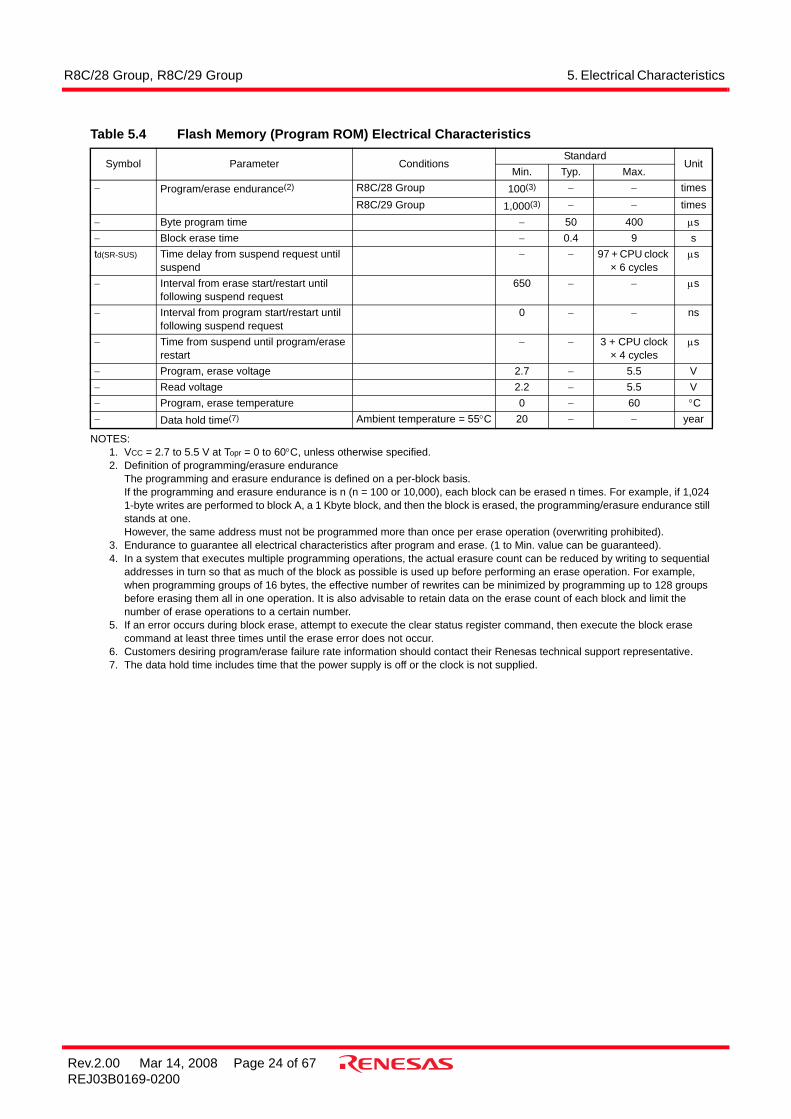
NOTES:1. VCC = 2.7 to 5.5 V at Topr = 0 to 60°C, unless otherwise specified.2. Definition of programming/erasure endurance
The programming and erasure endurance is defined on a per-block basis.If the programming and erasure endurance is n (n = 100 or 10,000), each block can be erased n times. For example, if 1,024 1-byte writes are performed to block A, a 1 Kbyte block, and then the block is erased, the programming/erasure endurance still stands at one.However, the same address must not be programmed more than once per erase operation (overwriting prohibited).
3. Endurance to guarantee all electrical characteristics after program and erase. (1 to Min. value can be guaranteed).4. In a system that executes multiple programming operations, the actual erasure count can be reduced by writing to sequential
addresses in turn so that as much of the block as possible is used up before performing an erase operation. For example, when programming groups of 16 bytes, the effective number of rewrites can be minimized by programming up to 128 groups before erasing them all in one operation. It is also advisable to retain data on the erase count of each block and limit the number of erase operations to a certain number.
5. If an error occurs during block erase, attempt to execute the clear status register command, then execute the block erase command at least three times until the erase error does not occur.
6. Customers desiring program/erase failure rate information should contact their Renesas technical support representative.7. The data hold time includes time that the power supply is off or the clock is not supplied.
Table 5.4 Flash Memory (Program ROM) Electrical Characteristics
Symbol Parameter ConditionsStandard
UnitMin. Typ. Max.
− Program/erase endurance(2) R8C/28 Group 100(3) − − timesR8C/29 Group 1,000(3) − − times
− Byte program time − 50 400 µs− Block erase time − 0.4 9 std(SR-SUS) Time delay from suspend request until
suspend− − 97 + CPU clock
× 6 cyclesµs
− Interval from erase start/restart until following suspend request
650 − − µs
− Interval from program start/restart until following suspend request
0 − − ns
− Time from suspend until program/erase restart
− − 3 + CPU clock × 4 cycles
µs
− Program, erase voltage 2.7 − 5.5 V− Read voltage 2.2 − 5.5 V− Program, erase temperature 0 − 60 °C− Data hold time(7) Ambient temperature = 55°C 20 − − year

R8C/28 Group, R8C/29 Group 5. Electrical Characteristics
Rev.2.00 Mar 14, 2008 Page 25 of 67REJ03B0169-0200
NOTES:1. VCC = 2.7 to 5.5 V at Topr = -20 to 85°C (N version) / -40 to 85°C (D version), unless otherwise specified.2. Definition of programming/erasure endurance
The programming and erasure endurance is defined on a per-block basis.If the programming and erasure endurance is n (n = 100 or 10,000), each block can be erased n times. For example, if 1,024 1-byte writes are performed to block A, a 1 Kbyte block, and then the block is erased, the programming/erasure endurance still stands at one. However, the same address must not be programmed more than once per erase operation (overwriting prohibited).
3. Endurance to guarantee all electrical characteristics after program and erase. (1 to Min. value can be guaranteed).4. Standard of block A and block B when program and erase endurance exceeds 1,000 times. Byte program time to 1,000 times
is the same as that in program ROM.5. In a system that executes multiple programming operations, the actual erasure count can be reduced by writing to sequential
addresses in turn so that as much of the block as possible is used up before performing an erase operation. For example, when programming groups of 16 bytes, the effective number of rewrites can be minimized by programming up to 128 groups before erasing them all in one operation. It is also advisable to retain data on the erase count of each block and limit the number of erase operations to a certain number.
6. If an error occurs during block erase, attempt to execute the clear status register command, then execute the block erase command at least three times until the erase error does not occur.
7. Customers desiring program/erase failure rate information should contact their Renesas technical support representative.8. -40°C for D version.9. The data hold time includes time that the power supply is off or the clock is not supplied.
Table 5.5 Flash Memory (Data flash Block A, Block B) Electrical Characteristics(4)
Symbol Parameter ConditionsStandard
UnitMin. Typ. Max.
− Program/erase endurance(2) 10,000(3) − − times− Byte program time
(program/erase endurance ≤ 1,000 times)− 50 400 µs
− Byte program time(program/erase endurance > 1,000 times)
− 65 − µs
− Block erase time(program/erase endurance ≤ 1,000 times)
− 0.2 9 s
− Block erase time(program/erase endurance > 1,000 times)
− 0.3 − s
td(SR-SUS) Time delay from suspend request until suspend
− − 97 + CPU clock × 6 cycles
µs
− Interval from erase start/restart until following suspend request
650 − − µs
− Interval from program start/restart until following suspend request
0 − − ns
− Time from suspend until program/erase restart
− − 3 + CPU clock × 4 cycles
µs
− Program, erase voltage 2.7 − 5.5 V− Read voltage 2.2 − 5.5 V− Program, erase temperature -20(8) − 85 °C− Data hold time(9) Ambient temperature = 55°C 20 − − year

R8C/28 Group, R8C/29 Group 5. Electrical Characteristics
Rev.2.00 Mar 14, 2008 Page 26 of 67REJ03B0169-0200
Figure 5.2 Time delay until Suspend
NOTES:1. The measurement condition is VCC = 2.2 to 5.5 V and Topr = -20 to 85°C (N version) / -40 to 85°C (D version).2. Necessary time until the voltage detection circuit operates when setting to 1 again after setting the VCA25 bit in the VCA2
register to 0.
NOTES:1. The measurement condition is VCC = 2.2 to 5.5 V and Topr = -20 to 85°C (N version) / -40 to 85°C (D version).2. Time until the voltage monitor 1 interrupt request is generated after the voltage passes Vdet1.3. Necessary time until the voltage detection circuit operates when setting to 1 again after setting the VCA26 bit in the VCA2
register to 0.4. This parameter shows the voltage detection level when the power supply drops.
The voltage detection level when the power supply rises is higher than the voltage detection level when the power supply drops by approximately 0.1 V.
NOTES:1. The measurement condition is VCC = 2.2 to 5.5 V and Topr = -20 to 85°C (N version) / -40 to 85°C (D version).2. Time until the voltage monitor 2 interrupt request is generated after the voltage passes Vdet2.3. Necessary time until the voltage detection circuit operates after setting to 1 again after setting the VCA27 bit in the VCA2
register to 0.
Table 5.6 Voltage Detection 0 Circuit Electrical Characteristics
Symbol Parameter ConditionStandard
UnitMin. Typ. Max.
Vdet0 Voltage detection level 2.2 2.3 2.4 V− Voltage detection circuit self power consumption VCA25 = 1, VCC = 5.0 V − 0.9 − µAtd(E-A) Waiting time until voltage detection circuit operation
starts(2)− − 300 µs
Vccmin MCU operating voltage minimum value 2.2 − − V
Table 5.7 Voltage Detection 1 Circuit Electrical Characteristics
Symbol Parameter ConditionStandard
UnitMin. Typ. Max.
Vdet1 Voltage detection level(4) 2.70 2.85 3.00 V− Voltage monitor 1 interrupt request generation time(2) − 40 − µs− Voltage detection circuit self power consumption VCA26 = 1, VCC = 5.0 V − 0.6 − µAtd(E-A) Waiting time until voltage detection circuit operation
starts(3)− − 100 µs
Table 5.8 Voltage Detection 2 Circuit Electrical Characteristics
Symbol Parameter ConditionStandard
UnitMin. Typ. Max.
Vdet2 Voltage detection level 3.3 3.6 3.9 V− Voltage monitor 2 interrupt request generation time(2) − 40 − µs− Voltage detection circuit self power consumption VCA27 = 1, VCC = 5.0 V − 0.6 − µAtd(E-A) Waiting time until voltage detection circuit operation
starts(3)− − 100 µs
FMR46
Suspend request(maskable interrupt request)
Fixed time
td(SR-SUS)
Clock-dependenttime
Access restart

R8C/28 Group, R8C/29 Group 5. Electrical Characteristics
Rev.2.00 Mar 14, 2008 Page 27 of 67REJ03B0169-0200
NOTES:1. The measurement condition is Topr = -20 to 85°C (N version) / -40 to 85°C (D version), unless otherwise specified.2. This condition (external power VCC rise gradient) does not apply if VCC ≥ 1.0 V.3. To use the power-on reset function, enable voltage monitor 0 reset by setting the LVD0ON bit in the OFS register to 0, the
VW0C0 and VW0C6 bits in the VW0C register to 1 respectively, and the VCA25 bit in the VCA2 register to 1.4. tw(por1) indicates the duration the external power VCC must be held below the effective voltage (Vpor1) to enable a power on
reset. When turning on the power for the first time, maintain tw(por1) for 30 s or more if -20°C ≤ Topr ≤ 85°C, maintain tw(por1) for3,000 s or more if -40°C ≤ Topr < -20°C.
Figure 5.3 Reset Circuit Electrical Characteristics
Table 5.9 Power-on Reset Circuit, Voltage Monitor 0 Reset Electrical Characteristics(3)
Symbol Parameter ConditionStandard
UnitMin. Typ. Max.
Vpor1 Power-on reset valid voltage(4) − − 0.1 VVpor2 Power-on reset or voltage monitor 0 reset valid
voltage0 − Vdet0 V
trth External power VCC rise gradient(2) 20 − − mV/msec
NOTES:1. When using the voltage monitor 0 digital filter, ensure that the voltage is within the MCU operation voltage
range (2.2 V or above) during the sampling time.2. The sampling clock can be selected. Refer to 6. Voltage Detection Circuit of Hardware Manual for details.3. Vdet0 indicates the voltage detection level of the voltage detection 0 circuit. Refer to 6. Voltage Detection
Circuit of Hardware Manual for details.
Vdet0(3)
Vpor1
Internalreset signal
(“L” valid)
tw(por1) Sampling time(1, 2)
Vdet0(3)
1fOCO-S
× 32 1fOCO-S
× 32
Vpor2
2.2 VExternal
Power VCCtrth
trth

R8C/28 Group, R8C/29 Group 5. Electrical Characteristics
Rev.2.00 Mar 14, 2008 Page 28 of 67REJ03B0169-0200
NOTES:1. VCC = 2.2 to 5.5 V, Topr = -20 to 85°C (N version) / -40 to 85°C (D version), unless otherwise specified.2. These standard values show when the FRA1 register value after reset is assumed.3. These standard values show when the corrected value of the FRA6 register is written to the FRA1 register.4. This enables the setting errors of bit rates such as 9600 bps and 38400 bps to be 0% when the serial interface is used in
UART mode.
NOTE:1. VCC = 2.2 to 5.5 V, Topr = -20 to 85°C (N version) / -40 to 85°C (D version), unless otherwise specified.
NOTES:1. The measurement condition is VCC = 2.2 to 5.5 V and Topr = 25°C.2. Waiting time until the internal power supply generation circuit stabilizes during power-on.3. Time until system clock supply starts after the interrupt is acknowledged to exit stop mode.
Table 5.10 High-speed On-Chip Oscillator Circuit Electrical Characteristics
Symbol Parameter ConditionStandard
UnitMin. Typ. Max.
fOCO40M High-speed on-chip oscillator frequency temperature • supply voltage dependence
VCC = 4.75 to 5.25 V0°C ≤ Topr ≤ 60°C(2)
39.2 40 40.8 MHz
VCC = 3.0 to 5.5 V-20°C ≤ Topr ≤ 85°C(2)
38.8 40 41.2 MHz
VCC = 3.0 to 5.5 V-40°C ≤ Topr ≤ 85°C(2)
38.4 40 41.6 MHz
VCC = 2.7 to 5.5 V-20°C ≤ Topr ≤ 85°C(2)
38 40 42 MHz
VCC = 2.7 to 5.5 V-40°C ≤ Topr ≤ 85°C(2)
37.6 40 42.4 MHz
VCC = 2.2 to 5.5 V-20°C ≤ Topr ≤ 85°C(3)
35.2 40 44.8 MHz
VCC = 2.2 to 5.5 V-40°C ≤ Topr ≤ 85°C(3)
34 40 46 MHz
VCC = 5.0 V ± 10%-20°C ≤ Topr ≤ 85°C(2)
38.8 40 40.8 MHz
VCC = 5.0 V ± 10%-40°C ≤ Topr ≤ 85°C(2)
38.4 40 40.8 MHz
High-speed on-chip oscillator frequency when correction value in FRA7 register is written to FRA1 register(4)
VCC = 5.0 V, Topr = 25°C − 36.864 − MHzVCC = 3.0 to 5.5 V-20°C ≤ Topr ≤ 85°C
-3% − 3% %
− Value in FRA1 register after reset 08h(3) − F7h(3) −
− Oscillation frequency adjustment unit of high-speed on-chip oscillator
Adjust FRA1 register (value after reset) to -1
− +0.3 − MHz
− Oscillation stability time − 10 100 µs− Self power consumption at oscillation VCC = 5.0 V, Topr = 25°C − 400 − µA
Table 5.11 Low-speed On-Chip Oscillator Circuit Electrical Characteristics
Symbol Parameter ConditionStandard
UnitMin. Typ. Max.
fOCO-S Low-speed on-chip oscillator frequency 30 125 250 kHz− Oscillation stability time − 10 100 µs− Self power consumption at oscillation VCC = 5.0 V, Topr = 25°C − 15 − µA
Table 5.12 Power Supply Circuit Timing Characteristics
Symbol Parameter ConditionStandard
UnitMin. Typ. Max.
td(P-R) Time for internal power supply stabilization during power-on(2)
1 − 2000 µs
td(R-S) STOP exit time(3) − − 150 µs

R8C/28 Group, R8C/29 Group 5. Electrical Characteristics
Rev.2.00 Mar 14, 2008 Page 29 of 67REJ03B0169-0200
NOTES:1. VCC = 2.2 to 5.5 V, VSS = 0 V at Topr = -20 to 85°C (N version) / -40 to 85°C (D version), unless otherwise specified.2. 1tCYC = 1/f1(s)
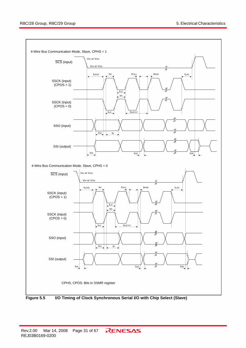
Table 5.13 Timing Requirements of Clock Synchronous Serial I/O with Chip Select(1)
Symbol Parameter ConditionsStandard Unit
Min. Typ. Max.tSUCYC SSCK clock cycle time 4 − − tCYC(2)
tHI SSCK clock “H” width 0.4 − 0.6 tSUCYC
tLO SSCK clock “L” width 0.4 − 0.6 tSUCYC
tRISE SSCK clock rising time
Master − − 1 tCYC(2)
Slave − − 1 µstFALL SSCK clock falling
time Master − − 1 tCYC(2)
Slave − − 1 µstSU SSO, SSI data input setup time 100 − − nstH SSO, SSI data input hold time 1 − − tCYC(2)
tLEAD SCS setup time Slave 1tCYC + 50 − − ns
tLAG SCS hold time Slave 1tCYC + 50 − − ns
tOD SSO, SSI data output delay time − − 1 tCYC(2)
tSA SSI slave access time 2.7 V ≤ VCC ≤ 5.5 V − − 1.5tCYC + 100 ns2.2 V ≤ VCC < 2.7 V − − 1.5tCYC + 200 ns
tOR SSI slave out open time 2.7 V ≤ VCC ≤ 5.5 V − − 1.5tCYC + 100 ns2.2 V ≤ VCC < 2.7 V − − 1.5tCYC + 200 ns

R8C/28 Group, R8C/29 Group 5. Electrical Characteristics
Rev.2.00 Mar 14, 2008 Page 30 of 67REJ03B0169-0200
Figure 5.4 I/O Timing of Clock Synchronous Serial I/O with Chip Select (Master)
VIH or VOH
VIH or VOH
tHI
tLO
tHI
tFALL tRISE
tLO tSUCYC
tOD
tHtSU
SCS (output)
SSCK (output)(CPOS = 1)
SSCK (output)(CPOS = 0)
SSO (output)
SSI (input)
4-Wire Bus Communication Mode, Master, CPHS = 1
VIH or VOH
VIH or VOH
tHI
tLO
tHI
tFALL tRISE
tLO tSUCYC
tOD
tHtSU
SCS (output)
SSCK (output)(CPOS = 1)
SSCK (output)(CPOS = 0)
SSO (output)
SSI (input)
4-Wire Bus Communication Mode, Master, CPHS = 0
CPHS, CPOS: Bits in SSMR register
R8C/28 Group, R8C/29 Group 5. Electrical Characteristics
Rev.2.00 Mar 14, 2008 Page 31 of 67REJ03B0169-0200
Figure 5.5 I/O Timing of Clock Synchronous Serial I/O with Chip Select (Slave)
VIH or VOH
VIH or VOH
SCS (input)
SSCK (input)(CPOS = 1)
SSCK (input)(CPOS = 0)
SSO (input)
SSI (output)
4-Wire Bus Communication Mode, Slave, CPHS = 1
VIH or VOH
VIH or VOH
tHI
tLO
tHI
tFALL tRISE
tLO tSUCYC
tHtSU
SCS (input)
SSCK (input)(CPOS = 1)
SSCK (input)(CPOS = 0)
SSO (input)
SSI (output)
4-Wire Bus Communication Mode, Slave, CPHS = 0
tOD
tLEAD
tSA
tLAG
tOR
tHI
tLO
tHI
tFALL tRISE
tLO tSUCYC
tHtSU
tOD
tLEAD
tSA
tLAG
tOR
CPHS, CPOS: Bits in SSMR register

R8C/28 Group, R8C/29 Group 5. Electrical Characteristics
Rev.2.00 Mar 14, 2008 Page 32 of 67REJ03B0169-0200
Figure 5.6 I/O Timing of Clock Synchronous Serial I/O with Chip Select (Clock Synchronous Communication Mode)
VIH or VOH
tHI
tLO tSUCYC
tOD
tHtSU
SSCK
SSO (output)
SSI (input)
VIH or VOH
R8C/28 Group, R8C/29 Group 5. Electrical Characteristics
Rev.2.00 Mar 14, 2008 Page 33 of 67REJ03B0169-0200
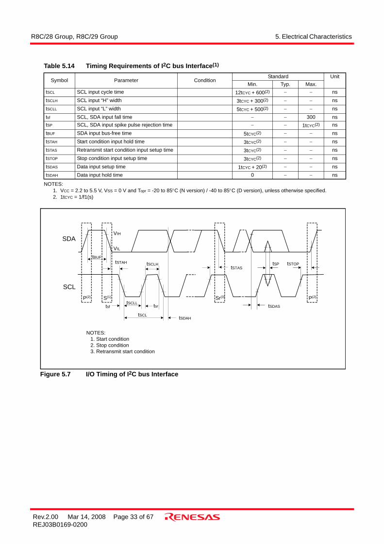
NOTES:1. VCC = 2.2 to 5.5 V, VSS = 0 V and Topr = -20 to 85°C (N version) / -40 to 85°C (D version), unless otherwise specified.2. 1tCYC = 1/f1(s)
Figure 5.7 I/O Timing of I2C bus Interface
Table 5.14 Timing Requirements of I2C bus Interface(1)
Symbol Parameter ConditionStandard Unit
Min. Typ. Max.tSCL SCL input cycle time 12tCYC + 600(2) − − nstSCLH SCL input “H” width 3tCYC + 300(2) − − nstSCLL SCL input “L” width 5tCYC + 500(2) − − nstsf SCL, SDA input fall time − − 300 nstSP SCL, SDA input spike pulse rejection time − − 1tCYC(2) nstBUF SDA input bus-free time 5tCYC(2) − − nstSTAH Start condition input hold time 3tCYC(2) − − nstSTAS Retransmit start condition input setup time 3tCYC(2) − − nstSTOP Stop condition input setup time 3tCYC(2) − − nstSDAS Data input setup time 1tCYC + 20(2) − − nstSDAH Data input hold time 0 − − ns
SDA
tSTAH
tSCLL
tBUF
VIH
VIL
tSCLH
SCL
tsrtsf
tSDAHtSCL
tSTAStSP tSTOP
tSDAS
P(2) S(1) Sr(3) P(2)
NOTES: 1. Start condition 2. Stop condition 3. Retransmit start condition
R8C/28 Group, R8C/29 Group 5. Electrical Characteristics
Rev.2.00 Mar 14, 2008 Page 34 of 67REJ03B0169-0200
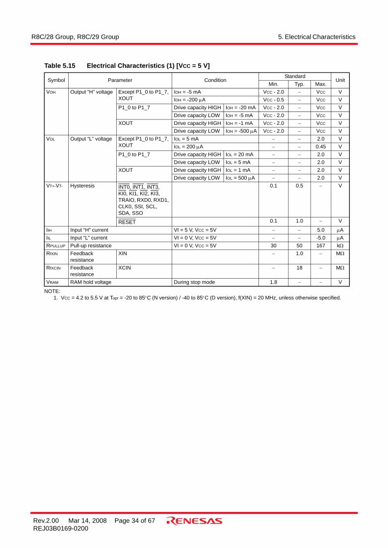
NOTE:1. VCC = 4.2 to 5.5 V at Topr = -20 to 85°C (N version) / -40 to 85°C (D version), f(XIN) = 20 MHz, unless otherwise specified.
Table 5.15 Electrical Characteristics (1) [VCC = 5 V]
Symbol Parameter ConditionStandard
UnitMin. Typ. Max.
VOH Output “H” voltage Except P1_0 to P1_7, XOUT
IOH = -5 mA VCC - 2.0 − VCC VIOH = -200 µA VCC - 0.5 − VCC V
P1_0 to P1_7 Drive capacity HIGH IOH = -20 mA VCC - 2.0 − VCC VDrive capacity LOW IOH = -5 mA VCC - 2.0 − VCC V
XOUT Drive capacity HIGH IOH = -1 mA VCC - 2.0 − VCC VDrive capacity LOW IOH = -500 µA VCC - 2.0 − VCC V
VOL Output “L” voltage Except P1_0 to P1_7, XOUT
IOL = 5 mA − − 2.0 VIOL = 200 µA − − 0.45 V
P1_0 to P1_7 Drive capacity HIGH IOL = 20 mA − − 2.0 VDrive capacity LOW IOL = 5 mA − − 2.0 V
XOUT Drive capacity HIGH IOL = 1 mA − − 2.0 VDrive capacity LOW IOL = 500 µA − − 2.0 V
VT+-VT- Hysteresis INT0, INT1, INT3, KI0, KI1, KI2, KI3, TRAIO, RXD0, RXD1, CLK0, SSI, SCL, SDA, SSO
0.1 0.5 − V
RESET 0.1 1.0 − V
IIH Input “H” current VI = 5 V, VCC = 5V − − 5.0 µAIIL Input “L” current VI = 0 V, VCC = 5V − − -5.0 µARPULLUP Pull-up resistance VI = 0 V, VCC = 5V 30 50 167 kΩRfXIN Feedback
resistanceXIN − 1.0 − MΩ
RfXCIN Feedback resistance
XCIN − 18 − MΩ
VRAM RAM hold voltage During stop mode 1.8 − − V
R8C/28 Group, R8C/29 Group 5. Electrical Characteristics
Rev.2.00 Mar 14, 2008 Page 35 of 67REJ03B0169-0200
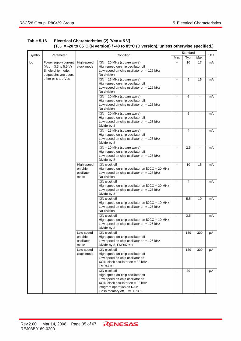
Table 5.16 Electrical Characteristics (2) [Vcc = 5 V](Topr = -20 to 85°C (N version) / -40 to 85°C (D version), unless otherwise specified.)
Symbol Parameter ConditionStandard
UnitMin. Typ. Max.
ICC Power supply current (VCC = 3.3 to 5.5 V)Single-chip mode, output pins are open, other pins are VSS
High-speed clock mode
XIN = 20 MHz (square wave)High-speed on-chip oscillator offLow-speed on-chip oscillator on = 125 kHzNo division
− 10 17 mA
XIN = 16 MHz (square wave)High-speed on-chip oscillator offLow-speed on-chip oscillator on = 125 kHzNo division
− 9 15 mA
XIN = 10 MHz (square wave)High-speed on-chip oscillator offLow-speed on-chip oscillator on = 125 kHzNo division
− 6 − mA
XIN = 20 MHz (square wave)High-speed on-chip oscillator offLow-speed on-chip oscillator on = 125 kHzDivide-by-8
− 5 − mA
XIN = 16 MHz (square wave)High-speed on-chip oscillator offLow-speed on-chip oscillator on = 125 kHzDivide-by-8
− 4 − mA
XIN = 10 MHz (square wave)High-speed on-chip oscillator offLow-speed on-chip oscillator on = 125 kHzDivide-by-8
− 2.5 − mA
High-speed on-chip oscillator mode
XIN clock offHigh-speed on-chip oscillator on fOCO = 20 MHzLow-speed on-chip oscillator on = 125 kHzNo division
− 10 15 mA
XIN clock offHigh-speed on-chip oscillator on fOCO = 20 MHzLow-speed on-chip oscillator on = 125 kHzDivide-by-8
− 4 − mA
XIN clock offHigh-speed on-chip oscillator on fOCO = 10 MHzLow-speed on-chip oscillator on = 125 kHzNo division
− 5.5 10 mA
XIN clock offHigh-speed on-chip oscillator on fOCO = 10 MHzLow-speed on-chip oscillator on = 125 kHzDivide-by-8
− 2.5 − mA
Low-speed on-chip oscillator mode
XIN clock offHigh-speed on-chip oscillator offLow-speed on-chip oscillator on = 125 kHzDivide-by-8, FMR47 = 1
− 130 300 µA
Low-speed clock mode
XIN clock offHigh-speed on-chip oscillator offLow-speed on-chip oscillator offXCIN clock oscillator on = 32 kHz FMR47 = 1
− 130 300 µA
XIN clock offHigh-speed on-chip oscillator offLow-speed on-chip oscillator offXCIN clock oscillator on = 32 kHz Program operation on RAMFlash memory off, FMSTP = 1
− 30 − µA
R8C/28 Group, R8C/29 Group 5. Electrical Characteristics
Rev.2.00 Mar 14, 2008 Page 36 of 67REJ03B0169-0200
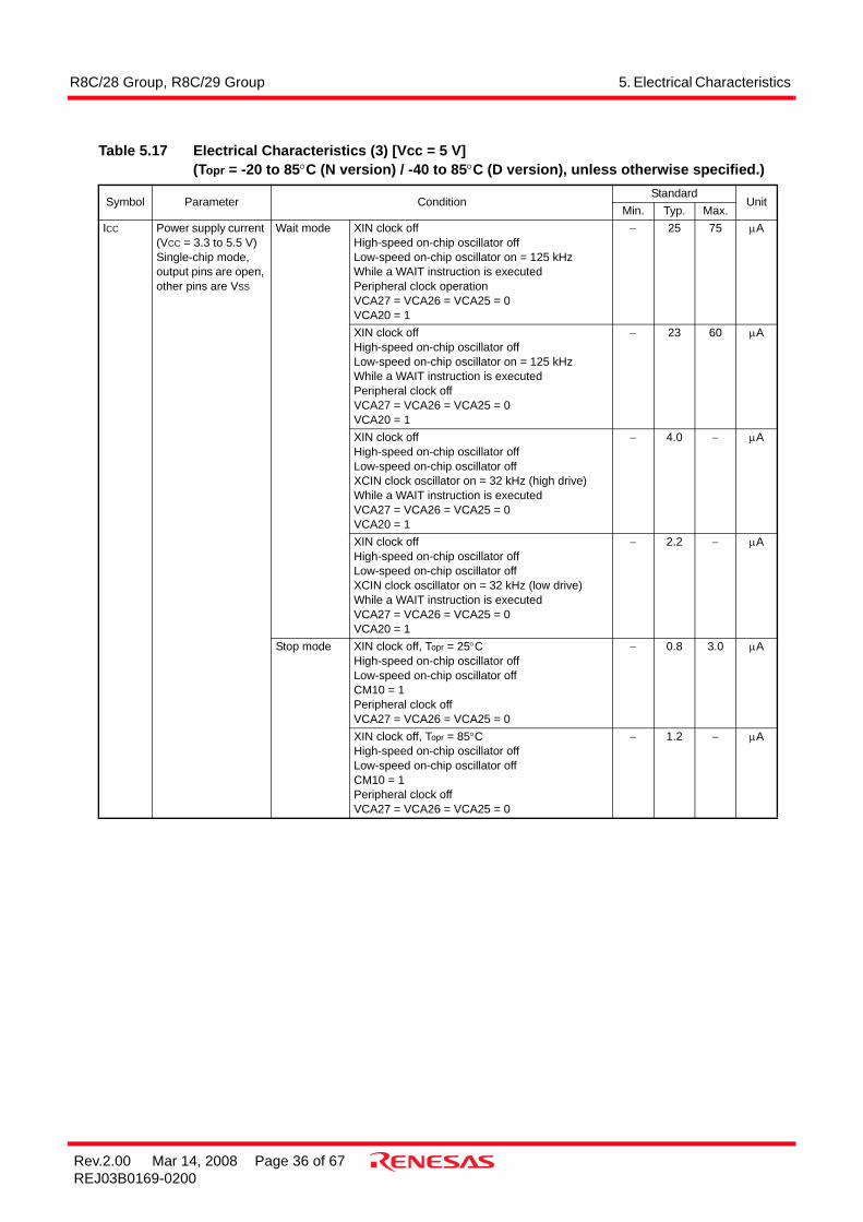
Table 5.17 Electrical Characteristics (3) [Vcc = 5 V](Topr = -20 to 85°C (N version) / -40 to 85°C (D version), unless otherwise specified.)
Symbol Parameter ConditionStandard
UnitMin. Typ. Max.
ICC Power supply current (VCC = 3.3 to 5.5 V)Single-chip mode, output pins are open, other pins are VSS
Wait mode XIN clock offHigh-speed on-chip oscillator offLow-speed on-chip oscillator on = 125 kHzWhile a WAIT instruction is executedPeripheral clock operationVCA27 = VCA26 = VCA25 = 0VCA20 = 1
− 25 75 µA
XIN clock offHigh-speed on-chip oscillator offLow-speed on-chip oscillator on = 125 kHzWhile a WAIT instruction is executedPeripheral clock offVCA27 = VCA26 = VCA25 = 0VCA20 = 1
− 23 60 µA
XIN clock offHigh-speed on-chip oscillator offLow-speed on-chip oscillator offXCIN clock oscillator on = 32 kHz (high drive)While a WAIT instruction is executedVCA27 = VCA26 = VCA25 = 0VCA20 = 1
− 4.0 − µA
XIN clock offHigh-speed on-chip oscillator offLow-speed on-chip oscillator offXCIN clock oscillator on = 32 kHz (low drive)While a WAIT instruction is executedVCA27 = VCA26 = VCA25 = 0VCA20 = 1
− 2.2 − µA
Stop mode XIN clock off, Topr = 25°CHigh-speed on-chip oscillator offLow-speed on-chip oscillator offCM10 = 1Peripheral clock offVCA27 = VCA26 = VCA25 = 0
− 0.8 3.0 µA
XIN clock off, Topr = 85°CHigh-speed on-chip oscillator offLow-speed on-chip oscillator offCM10 = 1Peripheral clock offVCA27 = VCA26 = VCA25 = 0
− 1.2 − µA

R8C/28 Group, R8C/29 Group 5. Electrical Characteristics
Rev.2.00 Mar 14, 2008 Page 37 of 67REJ03B0169-0200
Timing Requirements (Unless Otherwise Specified: VCC = 5 V, VSS = 0 V at Topr = 25°C) [VCC = 5 V]
Figure 5.8 XIN Input and XCIN Input Timing Diagram when VCC = 5 V
Figure 5.9 TRAIO Input Timing Diagram when VCC = 5 V
Table 5.18 XIN Input, XCIN Input
Symbol ParameterStandard
UnitMin. Max.
tc(XIN) XIN input cycle time 50 − nstWH(XIN) XIN input “H” width 25 − nstWL(XIN) XIN input “L” width 25 − nstc(XCIN) XCIN input cycle time 14 − µstWH(XCIN) XCIN input “H” width 7 − µstWL(XCIN) XCIN input “L” width 7 − µs
Table 5.19 TRAIO Input
Symbol ParameterStandard
UnitMin. Max.
tc(TRAIO) TRAIO input cycle time 100 − nstWH(TRAIO) TRAIO input “H” width 40 − nstWL(TRAIO) TRAIO input “L” width 40 − ns
XIN input
tWH(XIN)
tC(XIN)
tWL(XIN)
VCC = 5 V
TRAIO input
VCC = 5 VtC(TRAIO)
tWL(TRAIO)
tWH(TRAIO)

R8C/28 Group, R8C/29 Group 5. Electrical Characteristics
Rev.2.00 Mar 14, 2008 Page 38 of 67REJ03B0169-0200
i = 0 or 1
Figure 5.10 Serial Interface Timing Diagram when VCC = 5 V
NOTES:1. When selecting the digital filter by the INTi input filter select bit, use an INTi input HIGH width of either (1/digital filter clock
frequency × 3) or the minimum value of standard, whichever is greater.2. When selecting the digital filter by the INTi input filter select bit, use an INTi input LOW width of either (1/digital filter clock
frequency × 3) or the minimum value of standard, whichever is greater.
Figure 5.11 External Interrupt INTi Input Timing Diagram when VCC = 5 V
Table 5.20 Serial Interface
Symbol ParameterStandard
UnitMin. Max.
tc(CK) CLK0 input cycle time 200 − nstW(CKH) CLK0 input “H” width 100 − nstW(CKL) CLK0 input “L” width 100 − nstd(C-Q) TXDi output delay time − 50 nsth(C-Q) TXDi hold time 0 − nstsu(D-C) RXDi input setup time 50 − nsth(C-D) RXDi input hold time 90 − ns
Table 5.21 External Interrupt INTi (i = 0, 1, 3) Input
Symbol ParameterStandard
UnitMin. Max.
tW(INH) INTi input “H” width 250(1) − ns
tW(INL) INTi input “L” width 250(2) − ns
tW(CKH)
tC(CK)
tW(CKL)
th(C-Q)
th(C-D)tsu(D-C)td(C-Q)
CLK0
TXDi
RXDi
i = 0 or 1
VCC = 5 V
INTi input
tW(INL)
tW(INH)
i = 0, 1, 3
VCC = 5 V

R8C/28 Group, R8C/29 Group 5. Electrical Characteristics
Rev.2.00 Mar 14, 2008 Page 39 of 67REJ03B0169-0200
NOTE:1. VCC = 2.7 to 3.3 V at Topr = -20 to 85°C (N version) / -40 to 85°C (D version), f(XIN) = 10 MHz, unless otherwise specified.
Table 5.22 Electrical Characteristics (3) [VCC = 3 V]
Symbol Parameter ConditionStandard
UnitMin. Typ. Max.
VOH Output “H” voltage Except P1_0 to P1_7, XOUT
IOH = -1 mA VCC - 0.5 − VCC V
P1_0 to P1_7 Drive capacity HIGH
IOH = -5 mA VCC - 0.5 − VCC V
Drive capacity LOW
IOH = -1 mA VCC - 0.5 − VCC V
XOUT Drive capacity HIGH
IOH = -0.1 mA VCC - 0.5 − VCC V
Drive capacity LOW
IOH = -50 µA VCC - 0.5 − VCC V
VOL Output “L” voltage Except P1_0 to P1_7, XOUT
IOL = 1 mA − − 0.5 V
P1_0 to P1_7 Drive capacity HIGH
IOL = 5 mA − − 0.5 V
Drive capacity LOW
IOL = 1 mA − − 0.5 V
XOUT Drive capacity HIGH
IOL = 0.1 mA − − 0.5 V
Drive capacity LOW
IOL = 50 µA − − 0.5 V
VT+-VT- Hysteresis INT0, INT1, INT3, KI0, KI1, KI2, KI3, TRAIO, RXD0, RXD1, CLK0, SSI, SCL, SDA, SSO
0.1 0.3 − V
RESET 0.1 0.4 − V
IIH Input “H” current VI = 3 V, VCC = 3V − − 4.0 µAIIL Input “L” current VI = 0 V, VCC = 3V − − -4.0 µARPULLUP Pull-up resistance VI = 0 V, VCC = 3V 66 160 500 kΩRfXIN Feedback resistance XIN − 3.0 − MΩRfXCIN Feedback resistance XCIN − 18 − MΩVRAM RAM hold voltage During stop mode 1.8 − − V
R8C/28 Group, R8C/29 Group 5. Electrical Characteristics
Rev.2.00 Mar 14, 2008 Page 40 of 67REJ03B0169-0200
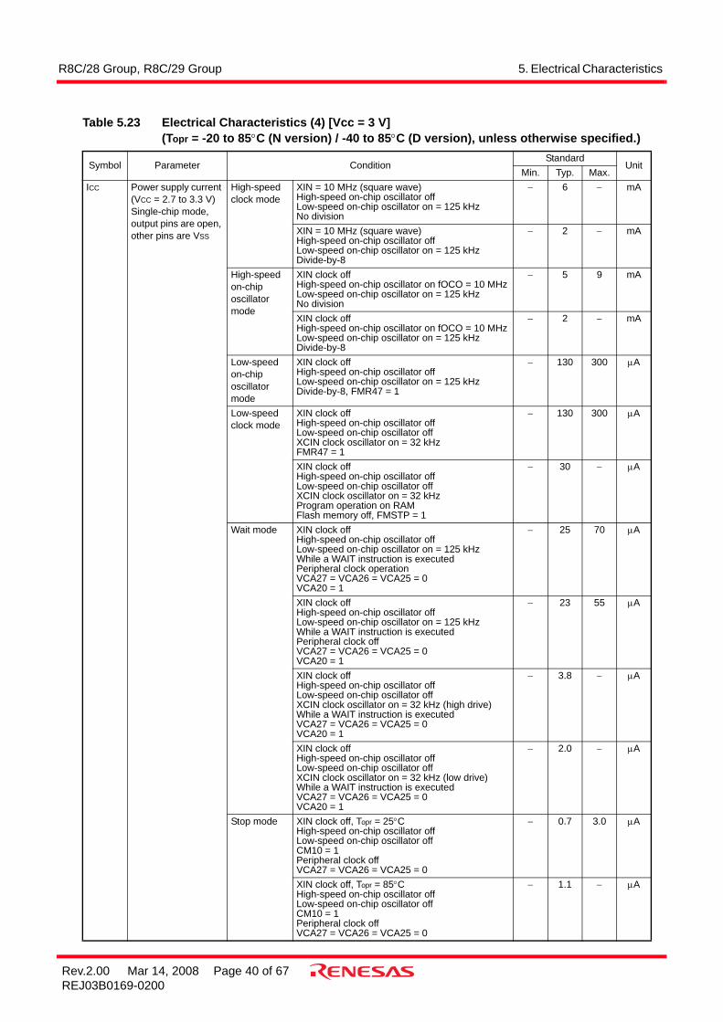
Table 5.23 Electrical Characteristics (4) [Vcc = 3 V](Topr = -20 to 85°C (N version) / -40 to 85°C (D version), unless otherwise specified.)
Symbol Parameter ConditionStandard
UnitMin. Typ. Max.
ICC Power supply current (VCC = 2.7 to 3.3 V)Single-chip mode, output pins are open, other pins are VSS
High-speed clock mode
XIN = 10 MHz (square wave)High-speed on-chip oscillator offLow-speed on-chip oscillator on = 125 kHzNo division
− 6 − mA
XIN = 10 MHz (square wave)High-speed on-chip oscillator offLow-speed on-chip oscillator on = 125 kHzDivide-by-8
− 2 − mA
High-speed on-chip oscillator mode
XIN clock offHigh-speed on-chip oscillator on fOCO = 10 MHzLow-speed on-chip oscillator on = 125 kHzNo division
− 5 9 mA
XIN clock offHigh-speed on-chip oscillator on fOCO = 10 MHzLow-speed on-chip oscillator on = 125 kHzDivide-by-8
− 2 − mA
Low-speed on-chip oscillator mode
XIN clock offHigh-speed on-chip oscillator offLow-speed on-chip oscillator on = 125 kHzDivide-by-8, FMR47 = 1
− 130 300 µA
Low-speed clock mode
XIN clock offHigh-speed on-chip oscillator offLow-speed on-chip oscillator offXCIN clock oscillator on = 32 kHz FMR47 = 1
− 130 300 µA
XIN clock offHigh-speed on-chip oscillator offLow-speed on-chip oscillator offXCIN clock oscillator on = 32 kHz Program operation on RAMFlash memory off, FMSTP = 1
− 30 − µA
Wait mode XIN clock offHigh-speed on-chip oscillator offLow-speed on-chip oscillator on = 125 kHzWhile a WAIT instruction is executedPeripheral clock operationVCA27 = VCA26 = VCA25 = 0VCA20 = 1
− 25 70 µA
XIN clock offHigh-speed on-chip oscillator offLow-speed on-chip oscillator on = 125 kHzWhile a WAIT instruction is executedPeripheral clock offVCA27 = VCA26 = VCA25 = 0VCA20 = 1
− 23 55 µA
XIN clock offHigh-speed on-chip oscillator offLow-speed on-chip oscillator offXCIN clock oscillator on = 32 kHz (high drive)While a WAIT instruction is executedVCA27 = VCA26 = VCA25 = 0VCA20 = 1
− 3.8 − µA
XIN clock offHigh-speed on-chip oscillator offLow-speed on-chip oscillator offXCIN clock oscillator on = 32 kHz (low drive)While a WAIT instruction is executedVCA27 = VCA26 = VCA25 = 0VCA20 = 1
− 2.0 − µA
Stop mode XIN clock off, Topr = 25°CHigh-speed on-chip oscillator offLow-speed on-chip oscillator offCM10 = 1Peripheral clock offVCA27 = VCA26 = VCA25 = 0
− 0.7 3.0 µA
XIN clock off, Topr = 85°CHigh-speed on-chip oscillator offLow-speed on-chip oscillator offCM10 = 1Peripheral clock offVCA27 = VCA26 = VCA25 = 0
− 1.1 − µA

R8C/28 Group, R8C/29 Group 5. Electrical Characteristics
Rev.2.00 Mar 14, 2008 Page 41 of 67REJ03B0169-0200
Timing requirements (Unless Otherwise Specified: VCC = 3 V, VSS = 0 V at Topr = 25°C) [VCC = 3 V]
Figure 5.12 XIN Input and XCIN Input Timing Diagram when VCC = 3 V
Figure 5.13 TRAIO Input Timing Diagram when VCC = 3 V
Table 5.24 XIN Input, XCIN Input
Symbol ParameterStandard
UnitMin. Max.
tc(XIN) XIN input cycle time 100 − nstWH(XIN) XIN input “H” width 40 − nstWL(XIN) XIN input “L” width 40 − nstc(XCIN) XCIN input cycle time 14 − µstWH(XCIN) XCIN input “H” width 7 − µstWL(XCIN) XCIN input “L” width 7 − µs
Table 5.25 TRAIO Input
Symbol ParameterStandard
UnitMin. Max.
tc(TRAIO) TRAIO input cycle time 300 − nstWH(TRAIO) TRAIO input “H” width 120 − nstWL(TRAIO) TRAIO input “L” width 120 − ns
XIN input
tWH(XIN)
tC(XIN)
tWL(XIN)
VCC = 3 V
TRAIO input
VCC = 3 VtC(TRAIO)
tWL(TRAIO)
tWH(TRAIO)
R8C/28 Group, R8C/29 Group 5. Electrical Characteristics
Rev.2.00 Mar 14, 2008 Page 42 of 67REJ03B0169-0200
i = 0 or 1
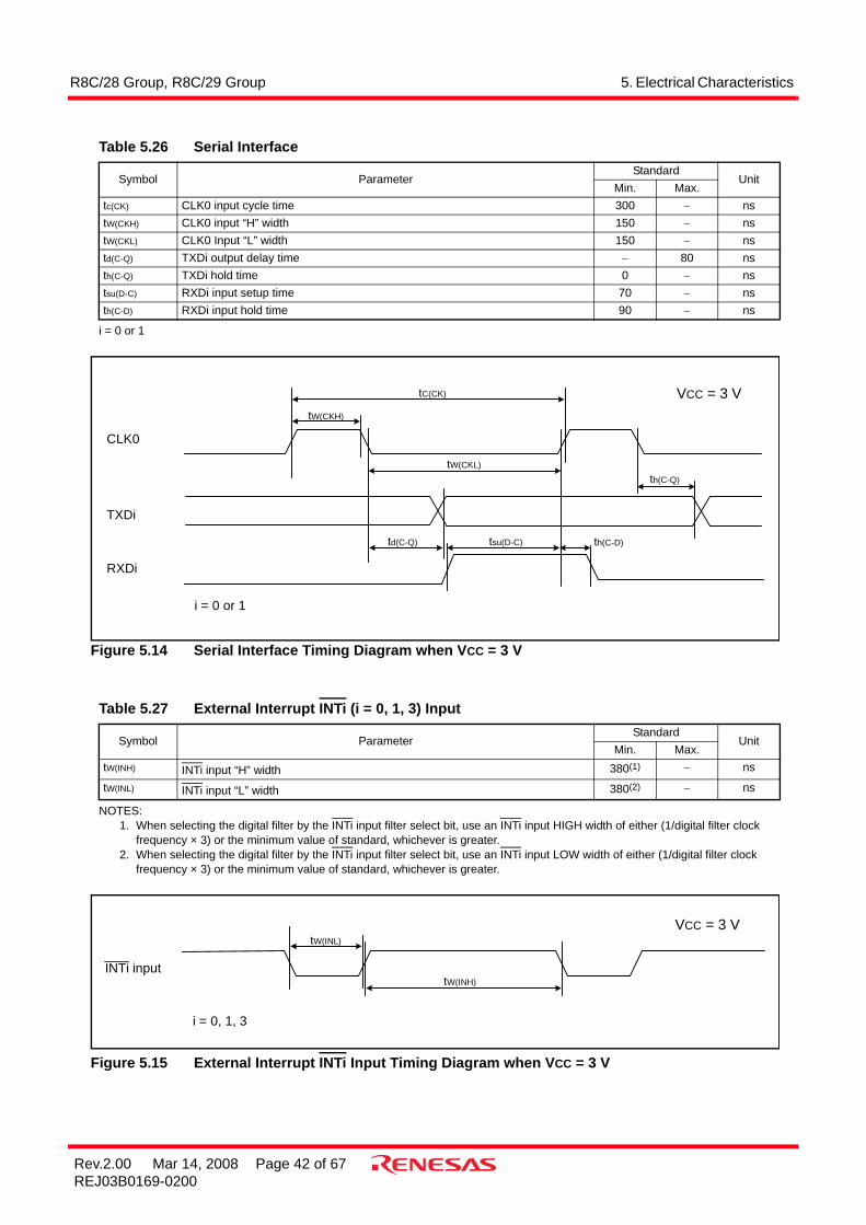
Figure 5.14 Serial Interface Timing Diagram when VCC = 3 V
NOTES:1. When selecting the digital filter by the INTi input filter select bit, use an INTi input HIGH width of either (1/digital filter clock
frequency × 3) or the minimum value of standard, whichever is greater.2. When selecting the digital filter by the INTi input filter select bit, use an INTi input LOW width of either (1/digital filter clock
frequency × 3) or the minimum value of standard, whichever is greater.
Figure 5.15 External Interrupt INTi Input Timing Diagram when VCC = 3 V
Table 5.26 Serial Interface
Symbol ParameterStandard
UnitMin. Max.
tc(CK) CLK0 input cycle time 300 − nstW(CKH) CLK0 input “H” width 150 − nstW(CKL) CLK0 Input “L” width 150 − nstd(C-Q) TXDi output delay time − 80 nsth(C-Q) TXDi hold time 0 − nstsu(D-C) RXDi input setup time 70 − nsth(C-D) RXDi input hold time 90 − ns
Table 5.27 External Interrupt INTi (i = 0, 1, 3) Input
Symbol ParameterStandard
UnitMin. Max.
tW(INH) INTi input “H” width 380(1) − ns
tW(INL) INTi input “L” width 380(2) − ns
tW(CKH)
tC(CK)
tW(CKL)
th(C-Q)
th(C-D)tsu(D-C)td(C-Q)
CLK0
TXDi
RXDi
VCC = 3 V
i = 0 or 1
INTi input
tW(INL)
tW(INH)
VCC = 3 V
i = 0, 1, 3

R8C/28 Group, R8C/29 Group 5. Electrical Characteristics
Rev.2.00 Mar 14, 2008 Page 43 of 67REJ03B0169-0200
NOTE:1. VCC = 2.2 V at Topr = -20 to 85°C (N version) / -40 to 85°C (D version), f(XIN) = 5 MHz, unless otherwise specified.
Table 5.28 Electrical Characteristics (5) [VCC = 2.2 V]
Symbol Parameter ConditionStandard
UnitMin. Typ. Max.
VOH Output “H” voltage Except P1_0 to P1_7, XOUT
IOH = -1 mA VCC - 0.5 − VCC V
P1_0 to P1_7 Drive capacity HIGH
IOH = -2 mA VCC - 0.5 − VCC V
Drive capacity LOW
IOH = -1 mA VCC - 0.5 − VCC V
XOUT Drive capacity HIGH
IOH = -0.1 mA VCC - 0.5 − VCC V
Drive capacity LOW
IOH = -50 µA VCC - 0.5 − VCC V
VOL Output “L” voltage Except P1_0 to P1_7, XOUT
IOL = 1 mA − − 0.5 V
P1_0 to P1_7 Drive capacity HIGH
IOL = 2 mA − − 0.5 V
Drive capacity LOW
IOL = 1 mA − − 0.5 V
XOUT Drive capacity HIGH
IOL = 0.1 mA − − 0.5 V
Drive capacity LOW
IOL = 50 µA − − 0.5 V
VT+-VT- Hysteresis INT0, INT1, INT3, KI0, KI1, KI2, KI3, TRAIO, RXD0, RXD1, CLK0, SSI, SCL, SDA, SSO
0.05 0.3 − V
RESET 0.05 0.15 − V
IIH Input “H” current VI = 2.2 V − − 4.0 µAIIL Input “L” current VI = 0 V − − -4.0 µARPULLUP Pull-up resistance VI = 0 V 100 200 600 kΩRfXIN Feedback resistance XIN − 5 − MΩRfXCIN Feedback resistance XCIN − 35 − MΩVRAM RAM hold voltage During stop mode 1.8 − − V

R8C/28 Group, R8C/29 Group 5. Electrical Characteristics
Rev.2.00 Mar 14, 2008 Page 44 of 67REJ03B0169-0200
Table 5.29 Electrical Characteristics (6) [Vcc = 2.2 V](Topr = -20 to 85°C (N version) / -40 to 85°C (D version), unless otherwise specified.)
Symbol Parameter ConditionStandard
UnitMin. Typ. Max.
ICC Power supply current (VCC = 2.2 to 2.7 V)Single-chip mode, output pins are open, other pins are VSS
High-speed clock mode
XIN = 5 MHz (square wave)High-speed on-chip oscillator offLow-speed on-chip oscillator on = 125 kHzNo division
− 3.5 − mA
XIN = 5 MHz (square wave)High-speed on-chip oscillator offLow-speed on-chip oscillator on = 125 kHzDivide-by-8
− 1.5 − mA
High-speed on-chip oscillator mode
XIN clock offHigh-speed on-chip oscillator on fOCO = 5 MHzLow-speed on-chip oscillator on = 125 kHzNo division
− 3.5 − mA
XIN clock offHigh-speed on-chip oscillator on fOCO = 5 MHzLow-speed on-chip oscillator on = 125 kHzDivide-by-8
− 1.5 − mA
Low-speed on-chip oscillator mode
XIN clock offHigh-speed on-chip oscillator offLow-speed on-chip oscillator on = 125 kHzDivide-by-8, FMR47 = 1
− 100 230 µA
Low-speed clock mode
XIN clock offHigh-speed on-chip oscillator offLow-speed on-chip oscillator offXCIN clock oscillator on = 32 kHz FMR47 = 1
− 100 230 µA
XIN clock offHigh-speed on-chip oscillator offLow-speed on-chip oscillator offXCIN clock oscillator on = 32 kHz Program operation on RAMFlash memory off, FMSTP = 1
− 25 − µA
Wait mode XIN clock offHigh-speed on-chip oscillator offLow-speed on-chip oscillator on = 125 kHzWhile a WAIT instruction is executedPeripheral clock operationVCA27 = VCA26 = VCA25 = 0VCA20 = 1
− 22 60 µA
XIN clock offHigh-speed on-chip oscillator offLow-speed on-chip oscillator on = 125 kHzWhile a WAIT instruction is executedPeripheral clock offVCA27 = VCA26 = VCA25 = 0VCA20 = 1
− 20 55 µA
XIN clock offHigh-speed on-chip oscillator offLow-speed on-chip oscillator offXCIN clock oscillator on = 32 kHz (high drive)While a WAIT instruction is executedVCA27 = VCA26 = VCA25 = 0VCA20 = 1
− 3.0 − µA
XIN clock offHigh-speed on-chip oscillator offLow-speed on-chip oscillator offXCIN clock oscillator on = 32 kHz (low drive)While a WAIT instruction is executedVCA27 = VCA26 = VCA25 = 0VCA20 = 1
− 1.8 − µA
Stop mode XIN clock off, Topr = 25°CHigh-speed on-chip oscillator offLow-speed on-chip oscillator offCM10 = 1Peripheral clock offVCA27 = VCA26 = VCA25 = 0
− 0.7 3.0 µA
XIN clock off, Topr = 85°CHigh-speed on-chip oscillator offLow-speed on-chip oscillator offCM10 = 1Peripheral clock offVCA27 = VCA26 = VCA25 = 0
− 1.1 − µA

R8C/28 Group, R8C/29 Group 5. Electrical Characteristics
Rev.2.00 Mar 14, 2008 Page 45 of 67REJ03B0169-0200
Timing requirements (Unless Otherwise Specified: VCC = 2.2 V, VSS = 0 V at Topr = 25°C) [VCC = 2.2 V]
Figure 5.16 XIN Input and XCIN Input Timing Diagram when VCC = 2.2 V
Figure 5.17 TRAIO Input Timing Diagram when VCC = 2.2 V
Table 5.30 XIN Input, XCIN Input
Symbol ParameterStandard
UnitMin. Max.
tc(XIN) XIN input cycle time 200 − nstWH(XIN) XIN input “H” width 90 − nstWL(XIN) XIN input “L” width 90 − nstc(XCIN) XCIN input cycle time 14 − µstWH(XCIN) XCIN input “H” width 7 − µstWL(XCIN) XCIN input “L” width 7 − µs
Table 5.31 TRAIO Input
Symbol ParameterStandard
UnitMin. Max.
tc(TRAIO) TRAIO input cycle time 500 − nstWH(TRAIO) TRAIO input “H” width 200 − nstWL(TRAIO) TRAIO input “L” width 200 − ns
XIN input
tWH(XIN)
tC(XIN)
tWL(XIN)
VCC = 2.2 V
TRAIO input
tC(TRAIO)
tWL(TRAIO)
tWH(TRAIO)
VCC = 2.2 V
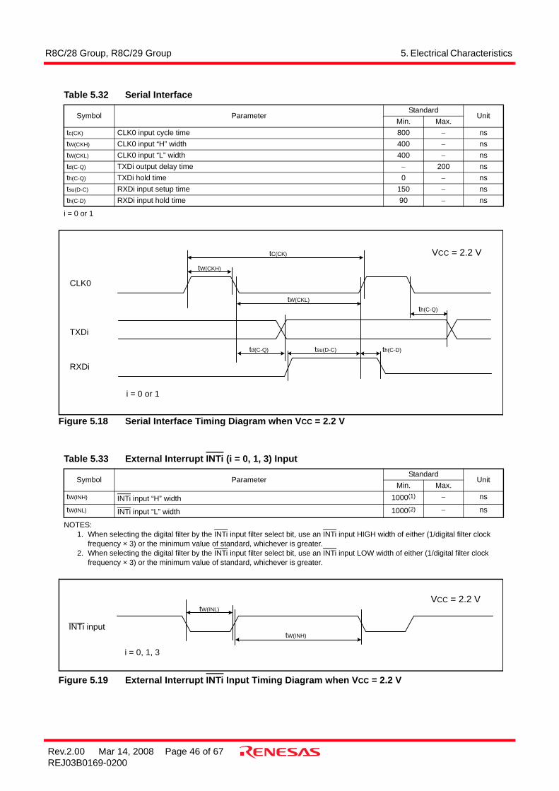
R8C/28 Group, R8C/29 Group 5. Electrical Characteristics
Rev.2.00 Mar 14, 2008 Page 46 of 67REJ03B0169-0200
i = 0 or 1
Figure 5.18 Serial Interface Timing Diagram when VCC = 2.2 V
NOTES:1. When selecting the digital filter by the INTi input filter select bit, use an INTi input HIGH width of either (1/digital filter clock
frequency × 3) or the minimum value of standard, whichever is greater.2. When selecting the digital filter by the INTi input filter select bit, use an INTi input LOW width of either (1/digital filter clock
frequency × 3) or the minimum value of standard, whichever is greater.
Figure 5.19 External Interrupt INTi Input Timing Diagram when VCC = 2.2 V
Table 5.32 Serial Interface
Symbol ParameterStandard
UnitMin. Max.
tc(CK) CLK0 input cycle time 800 − nstW(CKH) CLK0 input “H” width 400 − nstW(CKL) CLK0 input “L” width 400 − nstd(C-Q) TXDi output delay time − 200 nsth(C-Q) TXDi hold time 0 − nstsu(D-C) RXDi input setup time 150 − nsth(C-D) RXDi input hold time 90 − ns
Table 5.33 External Interrupt INTi (i = 0, 1, 3) Input
Symbol ParameterStandard
UnitMin. Max.
tW(INH) INTi input “H” width 1000(1) − ns
tW(INL) INTi input “L” width 1000(2) − ns
tW(CKH)
tC(CK)
tW(CKL)
th(C-Q)
th(C-D)tsu(D-C)td(C-Q)
CLK0
TXDi
RXDi
VCC = 2.2 V
i = 0 or 1
INTi input
tW(INL)
tW(INH)
VCC = 2.2 V
i = 0, 1, 3

R8C/28 Group, R8C/29 Group 5. Electrical Characteristics
Rev.2.00 Mar 14, 2008 Page 47 of 67REJ03B0169-0200
5.2 J, K Version
NOTES:1. VCC = 2.7 to 5.5 V at Topr = -40 to 85°C (J version) / -40 to 125°C (K version), unless otherwise specified.2. The average output current indicates the average value of current measured during 100 ms.
Table 5.34 Absolute Maximum RatingsSymbol Parameter Condition Rated Value Unit
VCC/AVCC Supply voltage -0.3 to 6.5 VVI Input voltage -0.3 to VCC + 0.3 VVO Output voltage -0.3 to VCC + 0.3 VPd Power dissipation -40 °C ≤ Topr ≤ 85 °C 300 mW
85 °C ≤ Topr ≤ 125 °C 125 mWTopr Operating ambient temperature -40 to 85 (J version) /
-40 to 125 (K version)°C
Tstg Storage temperature -65 to 150 °C
Table 5.35 Recommended Operating Conditions
Symbol Parameter ConditionsStandard
UnitMin. Typ. Max.
VCC/AVCC Supply voltage 2.7 − 5.5 VVSS/AVSS Supply voltage − 0 − VVIH Input “H” voltage 0.8 VCC − VCC VVIL Input “L” voltage 0 − 0.2 VCC VIOH(sum) Peak sum output
“H” currentSum of all pins IOH(peak)
− − -60 mA
IOH(peak) Peak output “H” current
− − -10 mA
IOH(avg) Average output “H” current
− − -5 mA
IOL(sum) Peak sum output “L” currents
Sum of all pins IOL(peak)
− − 60 mA
IOL(peak) Peak output “L” currents
− − 10 mA
IOL(avg) Average output “L” current
− − 5 mA
f(XIN) XIN clock input oscillation frequency 3.0 V ≤ VCC ≤ 5.5 V (other than K version)
0 − 20 MHz
3.0 V ≤ VCC ≤ 5.5 V (K version) 0 − 16 MHz2.7 V ≤ VCC < 3.0 V 0 − 10 MHz
− System clock OCD2 = 0XlN clock selected
3.0 V ≤ VCC ≤ 5.5 V (other than K version)
0 − 20 MHz
3.0 V ≤ VCC ≤ 5.5 V (K version) 0 − 16 MHz2.7 V ≤ VCC < 3.0 V 0 − 10 MHz
OCD2 = 1On-chip oscillator clock selected
FRA01 = 0Low-speed on-chip oscillator clock selected
− 125 − kHz
FRA01 = 1High-speed on-chip oscillator clock selected (other than K version)
− − 20 MHz
FRA01 = 1High-speed on-chip oscillator clock selected
− − 10 MHz
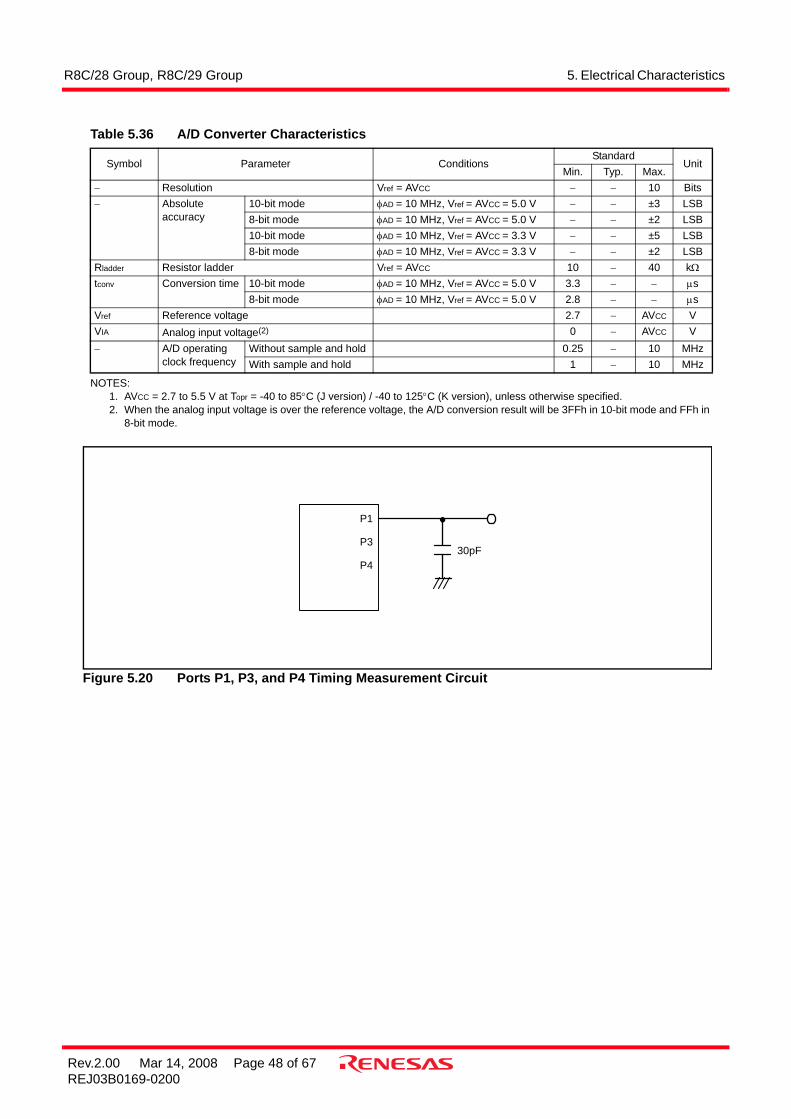
R8C/28 Group, R8C/29 Group 5. Electrical Characteristics
Rev.2.00 Mar 14, 2008 Page 48 of 67REJ03B0169-0200
NOTES:1. AVCC = 2.7 to 5.5 V at Topr = -40 to 85°C (J version) / -40 to 125°C (K version), unless otherwise specified.2. When the analog input voltage is over the reference voltage, the A/D conversion result will be 3FFh in 10-bit mode and FFh in
8-bit mode.
Figure 5.20 Ports P1, P3, and P4 Timing Measurement Circuit
Table 5.36 A/D Converter Characteristics
Symbol Parameter ConditionsStandard
UnitMin. Typ. Max.
− Resolution Vref = AVCC − − 10 Bits− Absolute
accuracy10-bit mode φAD = 10 MHz, Vref = AVCC = 5.0 V − − ±3 LSB8-bit mode φAD = 10 MHz, Vref = AVCC = 5.0 V − − ±2 LSB10-bit mode φAD = 10 MHz, Vref = AVCC = 3.3 V − − ±5 LSB8-bit mode φAD = 10 MHz, Vref = AVCC = 3.3 V − − ±2 LSB
Rladder Resistor ladder Vref = AVCC 10 − 40 kΩtconv Conversion time 10-bit mode φAD = 10 MHz, Vref = AVCC = 5.0 V 3.3 − − µs
8-bit mode φAD = 10 MHz, Vref = AVCC = 5.0 V 2.8 − − µsVref Reference voltage 2.7 − AVCC VVIA Analog input voltage(2) 0 − AVCC V− A/D operating
clock frequencyWithout sample and hold 0.25 − 10 MHzWith sample and hold 1 − 10 MHz
P1
P3
P430pF

R8C/28 Group, R8C/29 Group 5. Electrical Characteristics
Rev.2.00 Mar 14, 2008 Page 49 of 67REJ03B0169-0200
NOTES:1. VCC = 2.7 to 5.5 V at Topr = 0 to 60°C, unless otherwise specified.2. Definition of programming/erasure endurance
The programming and erasure endurance is defined on a per-block basis.If the programming and erasure endurance is n (n = 100 or 10,000), each block can be erased n times. For example, if 1,024 1-byte writes are performed to block A, a 1 Kbyte block, and then the block is erased, the programming/erasure endurance still stands at one.However, the same address must not be programmed more than once per erase operation (overwriting prohibited).
3. Endurance to guarantee all electrical characteristics after program and erase. (1 to Min. value can be guaranteed).4. In a system that executes multiple programming operations, the actual erasure count can be reduced by writing to sequential
addresses in turn so that as much of the block as possible is used up before performing an erase operation. For example, when programming groups of 16 bytes, the effective number of rewrites can be minimized by programming up to 128 groups before erasing them all in one operation. It is also advisable to retain data on the erase count of each block and limit the number of erase operations to a certain number.
5. If an error occurs during block erase, attempt to execute the clear status register command, then execute the block erase command at least three times until the erase error does not occur.
6. Customers desiring program/erase failure rate information should contact their Renesas technical support representative.7. The data hold time includes time that the power supply is off or the clock is not supplied.
Table 5.37 Flash Memory (Program ROM) Electrical Characteristics
Symbol Parameter ConditionsStandard
UnitMin. Typ. Max.
− Program/erase endurance(2) R8C/28 Group 100(3) − − timesR8C/29 Group 1,000(3) − − times
− Byte program time − 50 400 µs− Block erase time − 0.4 9 std(SR-SUS) Time delay from suspend request until
suspend− − 97 + CPU clock
× 6 cyclesµs
− Interval from erase start/restart until following suspend request
650 − − µs
− Interval from program start/restart until following suspend request
0 − − ns
− Time from suspend until program/erase restart
− − 3 + CPU clock × 4 cycles
µs
− Program, erase voltage 2.7 − 5.5 V− Read voltage 2.7 − 5.5 V− Program, erase temperature 0 − 60 °C− Data hold time(7) Ambient temperature = 55°C 20 − − year
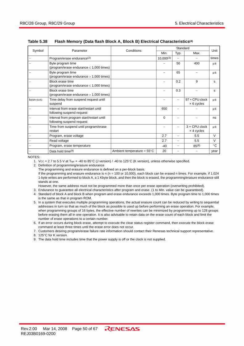
R8C/28 Group, R8C/29 Group 5. Electrical Characteristics
Rev.2.00 Mar 14, 2008 Page 50 of 67REJ03B0169-0200
NOTES:1. VCC = 2.7 to 5.5 V at Topr = -40 to 85°C (J version) / -40 to 125°C (K version), unless otherwise specified.2. Definition of programming/erasure endurance
The programming and erasure endurance is defined on a per-block basis.If the programming and erasure endurance is n (n = 100 or 10,000), each block can be erased n times. For example, if 1,024 1-byte writes are performed to block A, a 1 Kbyte block, and then the block is erased, the programming/erasure endurance still stands at one.However, the same address must not be programmed more than once per erase operation (overwriting prohibited).
3. Endurance to guarantee all electrical characteristics after program and erase. (1 to Min. value can be guaranteed).4. Standard of block A and block B when program and erase endurance exceeds 1,000 times. Byte program time to 1,000 times
is the same as that in program ROM.5. In a system that executes multiple programming operations, the actual erasure count can be reduced by writing to sequential
addresses in turn so that as much of the block as possible is used up before performing an erase operation. For example, when programming groups of 16 bytes, the effective number of rewrites can be minimized by programming up to 128 groups before erasing them all in one operation. It is also advisable to retain data on the erase count of each block and limit the number of erase operations to a certain number.
6. If an error occurs during block erase, attempt to execute the clear status register command, then execute the block erase command at least three times until the erase error does not occur.
7. Customers desiring program/erase failure rate information should contact their Renesas technical support representative.8. 125°C for K version.9. The data hold time includes time that the power supply is off or the clock is not supplied.
Table 5.38 Flash Memory (Data flash Block A, Block B) Electrical Characteristics(4)
Symbol Parameter ConditionsStandard
UnitMin. Typ. Max.
− Program/erase endurance(2) 10,000(3) − − times− Byte program time
(program/erase endurance ≤ 1,000 times)− 50 400 µs
− Byte program time(program/erase endurance > 1,000 times)
− 65 − µs
− Block erase time(program/erase endurance ≤ 1,000 times)
− 0.2 9 s
− Block erase time(program/erase endurance > 1,000 times)
− 0.3 − s
td(SR-SUS) Time delay from suspend request until suspend
− − 97 + CPU clock × 6 cycles
µs
− Interval from erase start/restart until following suspend request
650 − − µs
− Interval from program start/restart until following suspend request
0 − − ns
− Time from suspend until program/erase restart
− − 3 + CPU clock × 4 cycles
µs
− Program, erase voltage 2.7 − 5.5 V− Read voltage 2.7 − 5.5 V− Program, erase temperature -40 − 85(8) °C− Data hold time(9) Ambient temperature = 55°C 20 − − year
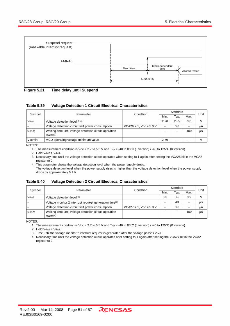
R8C/28 Group, R8C/29 Group 5. Electrical Characteristics
Rev.2.00 Mar 14, 2008 Page 51 of 67REJ03B0169-0200
Figure 5.21 Time delay until Suspend
NOTES:1. The measurement condition is VCC = 2.7 to 5.5 V and Topr = -40 to 85°C (J version) / -40 to 125°C (K version).2. Hold Vdet2 > Vdet1.3. Necessary time until the voltage detection circuit operates when setting to 1 again after setting the VCA26 bit in the VCA2
register to 0.4. This parameter shows the voltage detection level when the power supply drops.
The voltage detection level when the power supply rises is higher than the voltage detection level when the power supply drops by approximately 0.1 V.
NOTES:1. The measurement condition is VCC = 2.7 to 5.5 V and Topr = -40 to 85°C (J version) / -40 to 125°C (K version).2. Hold Vdet2 > Vdet1.3. Time until the voltage monitor 2 interrupt request is generated after the voltage passes Vdet2.4. Necessary time until the voltage detection circuit operates after setting to 1 again after setting the VCA27 bit in the VCA2
register to 0.
Table 5.39 Voltage Detection 1 Circuit Electrical Characteristics
Symbol Parameter ConditionStandard
UnitMin. Typ. Max.
Vdet1 Voltage detection level(2, 4) 2.70 2.85 3.0 V− Voltage detection circuit self power consumption VCA26 = 1, VCC = 5.0 V − 0.6 − µAtd(E-A) Waiting time until voltage detection circuit operation
starts(3)− − 100 µs
Vccmin MCU operating voltage minimum value 2.70 − − V
Table 5.40 Voltage Detection 2 Circuit Electrical Characteristics
Symbol Parameter ConditionStandard
UnitMin. Typ. Max.
Vdet2 Voltage detection level(2) 3.3 3.6 3.9 V− Voltage monitor 2 interrupt request generation time(3) − 40 − µs− Voltage detection circuit self power consumption VCA27 = 1, VCC = 5.0 V − 0.6 − µAtd(E-A) Waiting time until voltage detection circuit operation
starts(4)− − 100 µs
FMR46
Suspend request(maskable interrupt request)
Fixed time
td(SR-SUS)
Clock-dependenttime
Access restart
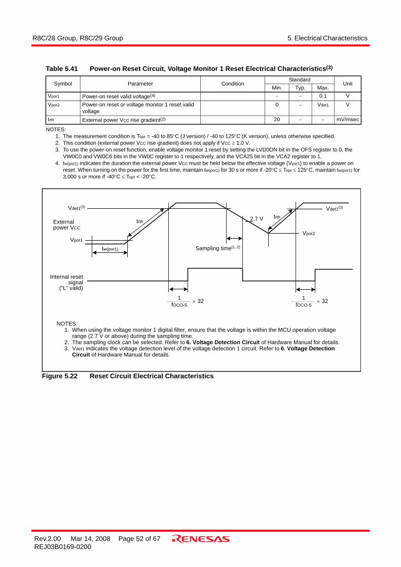
R8C/28 Group, R8C/29 Group 5. Electrical Characteristics
Rev.2.00 Mar 14, 2008 Page 52 of 67REJ03B0169-0200
NOTES:1. The measurement condition is Topr = -40 to 85°C (J version) / -40 to 125°C (K version), unless otherwise specified.2. This condition (external power VCC rise gradient) does not apply if VCC ≥ 1.0 V.3. To use the power-on reset function, enable voltage monitor 1 reset by setting the LVD0ON bit in the OFS register to 0, the
VW0C0 and VW0C6 bits in the VW0C register to 1 respectively, and the VCA25 bit in the VCA2 register to 1.4. tw(por1) indicates the duration the external power VCC must be held below the effective voltage (Vpor1) to enable a power on
reset. When turning on the power for the first time, maintain tw(por1) for 30 s or more if -20°C ≤ Topr ≤ 125°C, maintain tw(por1) for 3,000 s or more if -40°C ≤ Topr < -20°C.
Figure 5.22 Reset Circuit Electrical Characteristics
Table 5.41 Power-on Reset Circuit, Voltage Monitor 1 Reset Electrical Characteristics(3)
Symbol Parameter ConditionStandard
UnitMin. Typ. Max.
Vpor1 Power-on reset valid voltage(4) − − 0.1 VVpor2 Power-on reset or voltage monitor 1 reset valid
voltage0 − Vdet1 V
trth External power VCC rise gradient(2) 20 − − mV/msec
Vdet1(3)
Vpor1
Internal resetsignal
(“L” valid)
tw(por1) Sampling time(1, 2)
Vdet1(3)
Vpor2
× 321fOCO-S
× 321fOCO-S
2.7 Vtrthtrth
Externalpower VCC
NOTES:1. When using the voltage monitor 1 digital filter, ensure that the voltage is within the MCU operation voltage
range (2.7 V or above) during the sampling time.2. The sampling clock can be selected. Refer to 6. Voltage Detection Circuit of Hardware Manual for details.3. Vdet1 indicates the voltage detection level of the voltage detection 1 circuit. Refer to 6. Voltage Detection
Circuit of Hardware Manual for details.

R8C/28 Group, R8C/29 Group 5. Electrical Characteristics
Rev.2.00 Mar 14, 2008 Page 53 of 67REJ03B0169-0200
NOTES:1. VCC = 2.7 to 5.5 V, Topr = -40 to 85°C (J version) / -40 to 125°C (K version), unless otherwise specified.2. These standard values show when the FRA1 register value after reset is assumed.
NOTE:1. VCC = 2.7 to 5.5 V, Topr = -40 to 85°C (J version) / -40 to 125°C (K version), unless otherwise specified.
NOTES:1. The measurement condition is VCC = 2.7 to 5.5 V and Topr = 25°C.2. Waiting time until the internal power supply generation circuit stabilizes during power-on.3. Time until system clock supply starts after the interrupt is acknowledged to exit stop mode.
Table 5.42 High-speed On-Chip Oscillator Circuit Electrical Characteristics
Symbol Parameter ConditionStandard
UnitMin. Typ. Max.
fOCO40M High-speed on-chip oscillator frequency temperature • supply voltage dependence
VCC = 4.75 to 5.25 V0°C ≤ Topr ≤ 60°C(2)
39.2 40 40.8 MHz
VCC = 3.0 to 5.5 V-20°C ≤ Topr ≤ 85°C(2)
38.8 40 41.2 MHz
VCC = 3.0 to 5.5 V-40°C ≤ Topr ≤ 85°C(2)
38.4 40 41.6 MHz
VCC = 3.0 to 5.5 V-40°C ≤ Topr ≤ 125°C(2)
38 40 42 MHz
VCC = 2.7 to 5.5 V-40°C ≤ Topr ≤ 125°C(2)
37.6 40 42.4 MHz
− Value in FRA1 register after reset 08h − F7h −− Oscillation frequency adjustment unit of high-
speed on-chip oscillator Adjust FRA1 register (value after reset) to -1
− +0.3 − MHz
− Oscillation stability time − 10 100 µs− Self power consumption at oscillation VCC = 5.0 V, Topr = 25°C − 400 − µA
Table 5.43 Low-speed On-Chip Oscillator Circuit Electrical Characteristics
Symbol Parameter ConditionStandard
UnitMin. Typ. Max.
fOCO-S Low-speed on-chip oscillator frequency 40 125 250 kHz− Oscillation stability time − 10 100 µs− Self power consumption at oscillation VCC = 5.0 V, Topr = 25°C − 15 − µA
Table 5.44 Power Supply Circuit Timing Characteristics
Symbol Parameter ConditionStandard
UnitMin. Typ. Max.
td(P-R) Time for internal power supply stabilization during power-on(2)
1 − 2000 µs
td(R-S) STOP exit time(3) − − 150 µs

R8C/28 Group, R8C/29 Group 5. Electrical Characteristics
Rev.2.00 Mar 14, 2008 Page 54 of 67REJ03B0169-0200
NOTES:1. VCC = 2.7 to 5.5 V, VSS = 0 V at Topr = -40 to 85°C (J version) / -40 to 125°C (K version), unless otherwise specified.2. 1tCYC = 1/f1(s)
Table 5.45 Timing Requirements of Clock Synchronous Serial I/O with Chip Select(1)
Symbol Parameter ConditionsStandard Unit
Min. Typ. Max.tSUCYC SSCK clock cycle time 4 − − tCYC(2)
tHI SSCK clock “H” width 0.4 − 0.6 tSUCYC
tLO SSCK clock “L” width 0.4 − 0.6 tSUCYC
tRISE SSCK clock rising time
Master − − 1 tCYC(2)
Slave − − 1 µstFALL SSCK clock falling
time Master − − 1 tCYC(2)
Slave − − 1 µstSU SSO, SSI data input setup time 100 − − nstH SSO, SSI data input hold time 1 − − tCYC(2)
tLEAD SCS setup time Slave 1tCYC + 50 − − ns
tLAG SCS hold time Slave 1tCYC + 50 − − ns
tOD SSO, SSI data output delay time − − 1 tCYC(2)
tSA SSI slave access time − − 1.5tCYC + 100 nstOR SSI slave out open time − − 1.5tCYC + 100 ns
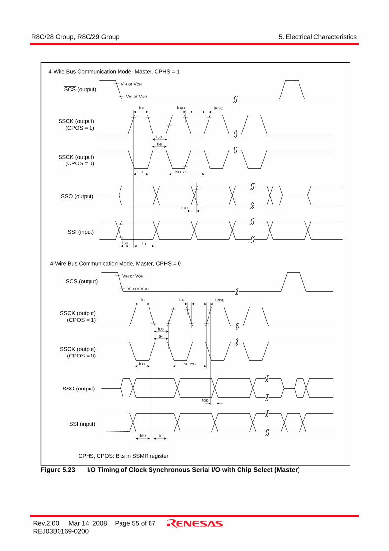
R8C/28 Group, R8C/29 Group 5. Electrical Characteristics
Rev.2.00 Mar 14, 2008 Page 55 of 67REJ03B0169-0200
Figure 5.23 I/O Timing of Clock Synchronous Serial I/O with Chip Select (Master)
VIH or VOH
VIH or VOH
tHI
tLO
tHI
tFALL tRISE
tLO tSUCYC
tOD
tHtSU
SCS (output)
SSCK (output)(CPOS = 1)
SSCK (output)(CPOS = 0)
SSO (output)
SSI (input)
4-Wire Bus Communication Mode, Master, CPHS = 1
VIH or VOH
VIH or VOH
tHI
tLO
tHI
tFALL tRISE
tLO tSUCYC
tOD
tHtSU
SCS (output)
SSCK (output)(CPOS = 1)
SSCK (output)(CPOS = 0)
SSO (output)
SSI (input)
4-Wire Bus Communication Mode, Master, CPHS = 0
CPHS, CPOS: Bits in SSMR register

R8C/28 Group, R8C/29 Group 5. Electrical Characteristics
Rev.2.00 Mar 14, 2008 Page 56 of 67REJ03B0169-0200
Figure 5.24 I/O Timing of Clock Synchronous Serial I/O with Chip Select (Slave)
VIH or VOH
VIH or VOH
SCS (input)
SSCK (input)(CPOS = 1)
SSCK (input)(CPOS = 0)
SSO (input)
SSI (output)
4-Wire Bus Communication Mode, Slave, CPHS = 1
VIH or VOH
VIH or VOH
tHI
tLO
tHI
tFALL tRISE
tLO tSUCYC
tHtSU
SCS (input)
SSCK (input)(CPOS = 1)
SSCK (input)(CPOS = 0)
SSO (input)
SSI (output)
4-Wire Bus Communication Mode, Slave, CPHS = 0
tOD
tLEAD
tSA
tLAG
tOR
tHI
tLO
tHI
tFALL tRISE
tLO tSUCYC
tHtSU
tOD
tLEAD
tSA
tLAG
tOR
CPHS, CPOS: Bits in SSMR register
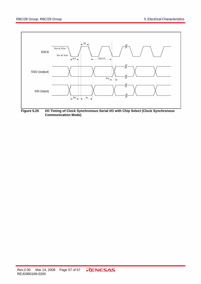
R8C/28 Group, R8C/29 Group 5. Electrical Characteristics
Rev.2.00 Mar 14, 2008 Page 57 of 67REJ03B0169-0200
Figure 5.25 I/O Timing of Clock Synchronous Serial I/O with Chip Select (Clock Synchronous Communication Mode)
VIH or VOH
tHI
tLO tSUCYC
tOD
tHtSU
SSCK
SSO (output)
SSI (input)
VIH or VOH

R8C/28 Group, R8C/29 Group 5. Electrical Characteristics
Rev.2.00 Mar 14, 2008 Page 58 of 67REJ03B0169-0200
NOTES:1. VCC = 2.7 to 5.5 V, VSS = 0 V at Topr = -40 to 85°C (J version) / -40 to 125°C (K version), unless otherwise specified.2. 1tCYC = 1/f1(s)
Figure 5.26 I/O Timing of I2C bus Interface
Table 5.46 Timing Requirements of I2C bus Interface(1)
Symbol Parameter ConditionStandard Unit
Min. Typ. Max.tSCL SCL input cycle time 12tCYC + 600(2) − − nstSCLH SCL input “H” width 3tCYC + 300(2) − − nstSCLL SCL input “L” width 5tCYC + 500(2) − − nstsf SCL, SDA input fall time − − 300 nstSP SCL, SDA input spike pulse rejection time − − 1tCYC(2) nstBUF SDA input bus-free time 5tCYC(2) − − nstSTAH Start condition input hold time 3tCYC(2) − − nstSTAS Retransmit start condition input setup time 3tCYC(2) − − nstSTOP Stop condition input setup time 3tCYC(2) − − nstSDAS Data input setup time 1tCYC + 20(2) − − nstSDAH Data input hold time 0 − − ns
SDA
tSTAH
tSCLL
tBUF
VIH
VIL
tSCLH
SCL
tsrtsf
tSDAHtSCL
tSTAStSP tSTOP
tSDAS
P(2) S(1) Sr(3) P(2)
NOTES: 1. Start condition 2. Stop condition 3. Retransmit start condition
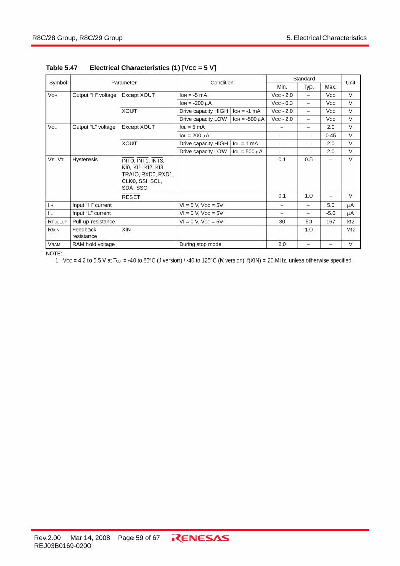
R8C/28 Group, R8C/29 Group 5. Electrical Characteristics
Rev.2.00 Mar 14, 2008 Page 59 of 67REJ03B0169-0200
NOTE:1. VCC = 4.2 to 5.5 V at Topr = -40 to 85°C (J version) / -40 to 125°C (K version), f(XIN) = 20 MHz, unless otherwise specified.
Table 5.47 Electrical Characteristics (1) [VCC = 5 V]
Symbol Parameter ConditionStandard
UnitMin. Typ. Max.
VOH Output “H” voltage Except XOUT IOH = -5 mA VCC - 2.0 − VCC VIOH = -200 µA VCC - 0.3 − VCC V
XOUT Drive capacity HIGH IOH = -1 mA VCC - 2.0 − VCC VDrive capacity LOW IOH = -500 µA VCC - 2.0 − VCC V
VOL Output “L” voltage Except XOUT IOL = 5 mA − − 2.0 VIOL = 200 µA − − 0.45 V
XOUT Drive capacity HIGH IOL = 1 mA − − 2.0 VDrive capacity LOW IOL = 500 µA − − 2.0 V
VT+-VT- Hysteresis INT0, INT1, INT3, KI0, KI1, KI2, KI3, TRAIO, RXD0, RXD1, CLK0, SSI, SCL, SDA, SSO
0.1 0.5 − V
RESET 0.1 1.0 − V
IIH Input “H” current VI = 5 V, VCC = 5V − − 5.0 µAIIL Input “L” current VI = 0 V, VCC = 5V − − -5.0 µARPULLUP Pull-up resistance VI = 0 V, VCC = 5V 30 50 167 kΩRfXIN Feedback
resistanceXIN − 1.0 − MΩ
VRAM RAM hold voltage During stop mode 2.0 − − V
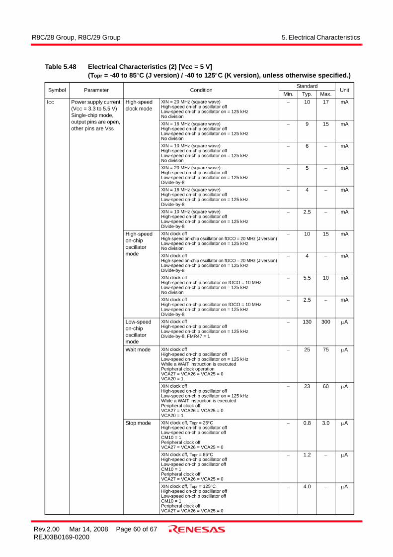
R8C/28 Group, R8C/29 Group 5. Electrical Characteristics
Rev.2.00 Mar 14, 2008 Page 60 of 67REJ03B0169-0200
Table 5.48 Electrical Characteristics (2) [Vcc = 5 V](Topr = -40 to 85°C (J version) / -40 to 125°C (K version), unless otherwise specified.)
Symbol Parameter ConditionStandard
UnitMin. Typ. Max.
ICC Power supply current (VCC = 3.3 to 5.5 V)Single-chip mode, output pins are open, other pins are VSS
High-speed clock mode
XIN = 20 MHz (square wave)High-speed on-chip oscillator offLow-speed on-chip oscillator on = 125 kHzNo division
− 10 17 mA
XIN = 16 MHz (square wave)High-speed on-chip oscillator offLow-speed on-chip oscillator on = 125 kHzNo division
− 9 15 mA
XIN = 10 MHz (square wave)High-speed on-chip oscillator offLow-speed on-chip oscillator on = 125 kHzNo division
− 6 − mA
XIN = 20 MHz (square wave)High-speed on-chip oscillator offLow-speed on-chip oscillator on = 125 kHzDivide-by-8
− 5 − mA
XIN = 16 MHz (square wave)High-speed on-chip oscillator offLow-speed on-chip oscillator on = 125 kHzDivide-by-8
− 4 − mA
XIN = 10 MHz (square wave)High-speed on-chip oscillator offLow-speed on-chip oscillator on = 125 kHzDivide-by-8
− 2.5 − mA
High-speed on-chip oscillator mode
XIN clock offHigh-speed on-chip oscillator on fOCO = 20 MHz (J version)Low-speed on-chip oscillator on = 125 kHzNo division
− 10 15 mA
XIN clock offHigh-speed on-chip oscillator on fOCO = 20 MHz (J version)Low-speed on-chip oscillator on = 125 kHzDivide-by-8
− 4 − mA
XIN clock offHigh-speed on-chip oscillator on fOCO = 10 MHzLow-speed on-chip oscillator on = 125 kHzNo division
− 5.5 10 mA
XIN clock offHigh-speed on-chip oscillator on fOCO = 10 MHzLow-speed on-chip oscillator on = 125 kHzDivide-by-8
− 2.5 − mA
Low-speed on-chip oscillator mode
XIN clock offHigh-speed on-chip oscillator offLow-speed on-chip oscillator on = 125 kHzDivide-by-8, FMR47 = 1
− 130 300 µA
Wait mode XIN clock offHigh-speed on-chip oscillator offLow-speed on-chip oscillator on = 125 kHzWhile a WAIT instruction is executedPeripheral clock operationVCA27 = VCA26 = VCA25 = 0VCA20 = 1
− 25 75 µA
XIN clock offHigh-speed on-chip oscillator offLow-speed on-chip oscillator on = 125 kHzWhile a WAIT instruction is executedPeripheral clock offVCA27 = VCA26 = VCA25 = 0VCA20 = 1
− 23 60 µA
Stop mode XIN clock off, Topr = 25°CHigh-speed on-chip oscillator offLow-speed on-chip oscillator offCM10 = 1Peripheral clock offVCA27 = VCA26 = VCA25 = 0
− 0.8 3.0 µA
XIN clock off, Topr = 85°CHigh-speed on-chip oscillator offLow-speed on-chip oscillator offCM10 = 1Peripheral clock offVCA27 = VCA26 = VCA25 = 0
− 1.2 − µA
XIN clock off, Topr = 125°CHigh-speed on-chip oscillator offLow-speed on-chip oscillator offCM10 = 1Peripheral clock offVCA27 = VCA26 = VCA25 = 0
− 4.0 − µA
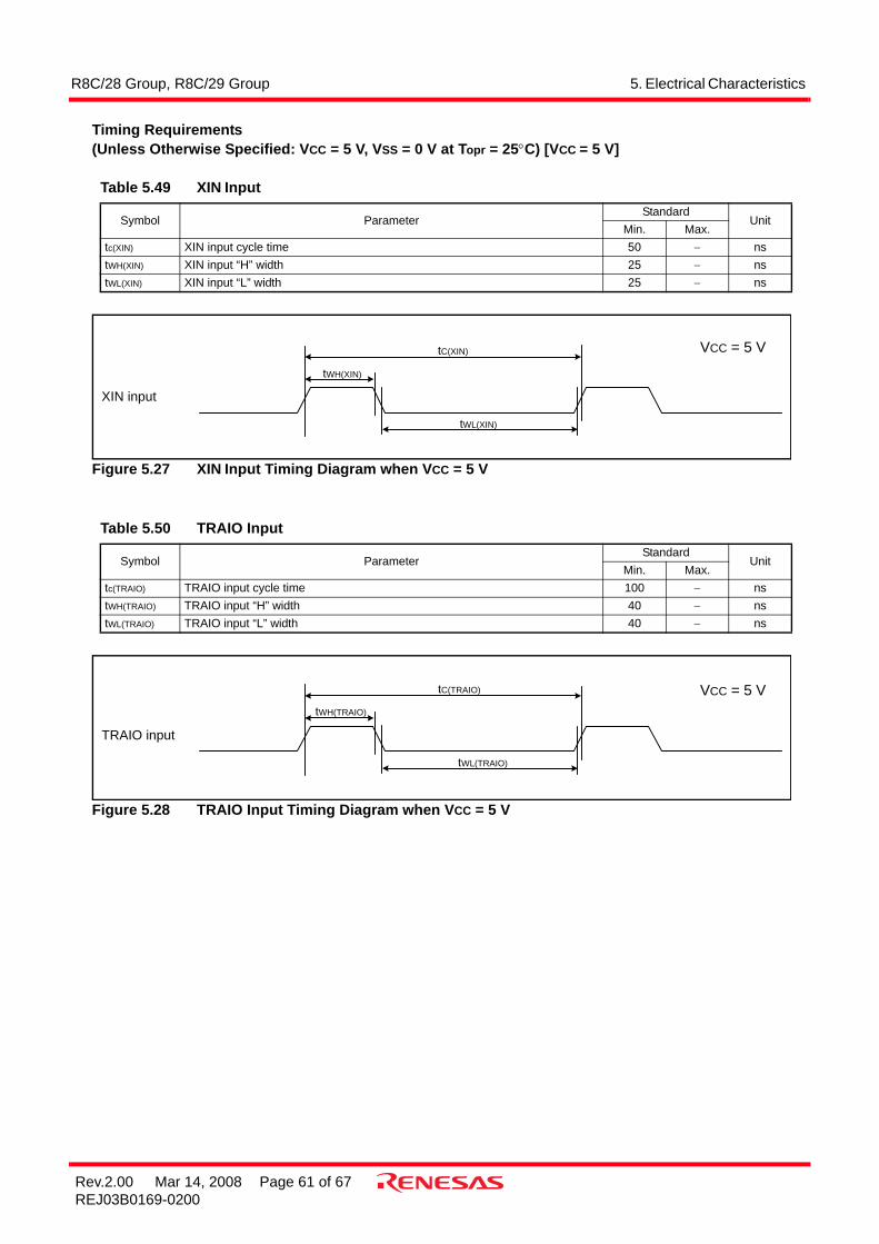
R8C/28 Group, R8C/29 Group 5. Electrical Characteristics
Rev.2.00 Mar 14, 2008 Page 61 of 67REJ03B0169-0200
Timing Requirements (Unless Otherwise Specified: VCC = 5 V, VSS = 0 V at Topr = 25°C) [VCC = 5 V]
Figure 5.27 XIN Input Timing Diagram when VCC = 5 V
Figure 5.28 TRAIO Input Timing Diagram when VCC = 5 V
Table 5.49 XIN Input
Symbol ParameterStandard
UnitMin. Max.
tc(XIN) XIN input cycle time 50 − nstWH(XIN) XIN input “H” width 25 − nstWL(XIN) XIN input “L” width 25 − ns
Table 5.50 TRAIO Input
Symbol ParameterStandard
UnitMin. Max.
tc(TRAIO) TRAIO input cycle time 100 − nstWH(TRAIO) TRAIO input “H” width 40 − nstWL(TRAIO) TRAIO input “L” width 40 − ns
XIN input
tWH(XIN)
tC(XIN)
tWL(XIN)
VCC = 5 V
TRAIO input
VCC = 5 VtC(TRAIO)
tWL(TRAIO)
tWH(TRAIO)
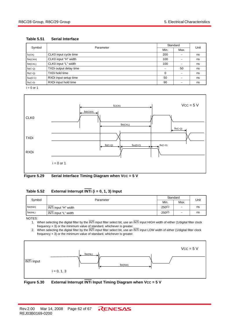
R8C/28 Group, R8C/29 Group 5. Electrical Characteristics
Rev.2.00 Mar 14, 2008 Page 62 of 67REJ03B0169-0200
i = 0 or 1
Figure 5.29 Serial Interface Timing Diagram when VCC = 5 V
NOTES:1. When selecting the digital filter by the INTi input filter select bit, use an INTi input HIGH width of either (1/digital filter clock
frequency × 3) or the minimum value of standard, whichever is greater.2. When selecting the digital filter by the INTi input filter select bit, use an INTi input LOW width of either (1/digital filter clock
frequency × 3) or the minimum value of standard, whichever is greater.
Figure 5.30 External Interrupt INTi Input Timing Diagram when VCC = 5 V
Table 5.51 Serial Interface
Symbol ParameterStandard
UnitMin. Max.
tc(CK) CLK0 input cycle time 200 − nstW(CKH) CLK0 input “H” width 100 − nstW(CKL) CLK0 input “L” width 100 − nstd(C-Q) TXDi output delay time − 50 nsth(C-Q) TXDi hold time 0 − nstsu(D-C) RXDi input setup time 50 − nsth(C-D) RXDi input hold time 90 − ns
Table 5.52 External Interrupt INTi (i = 0, 1, 3) Input
Symbol ParameterStandard
UnitMin. Max.
tW(INH) INTi input “H” width 250(1) − ns
tW(INL) INTi input “L” width 250(2) − ns
tW(CKH)
tC(CK)
tW(CKL)
th(C-Q)
th(C-D)tsu(D-C)td(C-Q)
CLK0
TXDi
RXDi
i = 0 or 1
VCC = 5 V
INTi input
tW(INL)
tW(INH)
i = 0, 1, 3
VCC = 5 V
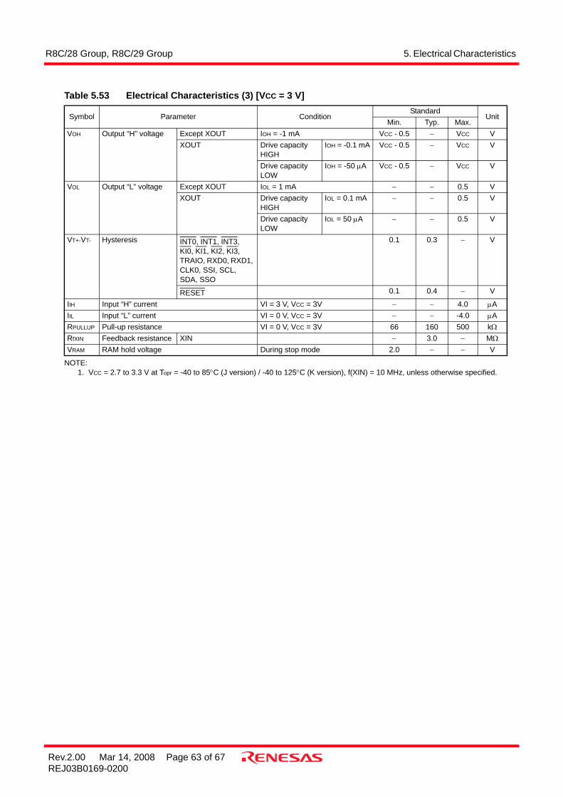
R8C/28 Group, R8C/29 Group 5. Electrical Characteristics
Rev.2.00 Mar 14, 2008 Page 63 of 67REJ03B0169-0200
NOTE:1. VCC = 2.7 to 3.3 V at Topr = -40 to 85°C (J version) / -40 to 125°C (K version), f(XIN) = 10 MHz, unless otherwise specified.
Table 5.53 Electrical Characteristics (3) [VCC = 3 V]
Symbol Parameter ConditionStandard
UnitMin. Typ. Max.
VOH Output “H” voltage Except XOUT IOH = -1 mA VCC - 0.5 − VCC VXOUT Drive capacity
HIGHIOH = -0.1 mA VCC - 0.5 − VCC V
Drive capacity LOW
IOH = -50 µA VCC - 0.5 − VCC V
VOL Output “L” voltage Except XOUT IOL = 1 mA − − 0.5 VXOUT Drive capacity
HIGHIOL = 0.1 mA − − 0.5 V
Drive capacity LOW
IOL = 50 µA − − 0.5 V
VT+-VT- Hysteresis INT0, INT1, INT3, KI0, KI1, KI2, KI3, TRAIO, RXD0, RXD1, CLK0, SSI, SCL, SDA, SSO
0.1 0.3 − V
RESET 0.1 0.4 − V
IIH Input “H” current VI = 3 V, VCC = 3V − − 4.0 µAIIL Input “L” current VI = 0 V, VCC = 3V − − -4.0 µARPULLUP Pull-up resistance VI = 0 V, VCC = 3V 66 160 500 kΩRfXIN Feedback resistance XIN − 3.0 − MΩVRAM RAM hold voltage During stop mode 2.0 − − V
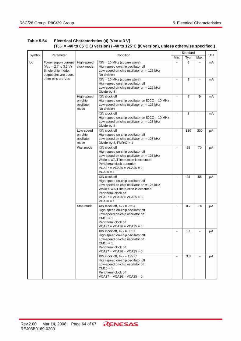
R8C/28 Group, R8C/29 Group 5. Electrical Characteristics
Rev.2.00 Mar 14, 2008 Page 64 of 67REJ03B0169-0200
Table 5.54 Electrical Characteristics (4) [Vcc = 3 V](Topr = -40 to 85°C (J version) / -40 to 125°C (K version), unless otherwise specified.)
Symbol Parameter ConditionStandard
UnitMin. Typ. Max.
ICC Power supply current (VCC = 2.7 to 3.3 V)Single-chip mode, output pins are open, other pins are VSS
High-speed clock mode
XIN = 10 MHz (square wave)High-speed on-chip oscillator offLow-speed on-chip oscillator on = 125 kHzNo division
− 6 − mA
XIN = 10 MHz (square wave)High-speed on-chip oscillator offLow-speed on-chip oscillator on = 125 kHzDivide-by-8
− 2 − mA
High-speed on-chip oscillator mode
XIN clock offHigh-speed on-chip oscillator on fOCO = 10 MHzLow-speed on-chip oscillator on = 125 kHzNo division
− 5 9 mA
XIN clock offHigh-speed on-chip oscillator on fOCO = 10 MHzLow-speed on-chip oscillator on = 125 kHzDivide-by-8
− 2 − mA
Low-speed on-chip oscillator mode
XIN clock offHigh-speed on-chip oscillator offLow-speed on-chip oscillator on = 125 kHzDivide-by-8, FMR47 = 1
− 130 300 µA
Wait mode XIN clock offHigh-speed on-chip oscillator offLow-speed on-chip oscillator on = 125 kHzWhile a WAIT instruction is executedPeripheral clock operationVCA27 = VCA26 = VCA25 = 0VCA20 = 1
− 25 70 µA
XIN clock offHigh-speed on-chip oscillator offLow-speed on-chip oscillator on = 125 kHzWhile a WAIT instruction is executedPeripheral clock offVCA27 = VCA26 = VCA25 = 0VCA20 = 1
− 23 55 µA
Stop mode XIN clock off, Topr = 25°CHigh-speed on-chip oscillator offLow-speed on-chip oscillator offCM10 = 1Peripheral clock offVCA27 = VCA26 = VCA25 = 0
− 0.7 3.0 µA
XIN clock off, Topr = 85°CHigh-speed on-chip oscillator offLow-speed on-chip oscillator offCM10 = 1Peripheral clock offVCA27 = VCA26 = VCA25 = 0
− 1.1 − µA
XIN clock off, Topr = 125°CHigh-speed on-chip oscillator offLow-speed on-chip oscillator offCM10 = 1Peripheral clock offVCA27 = VCA26 = VCA25 = 0
− 3.8 − µA

R8C/28 Group, R8C/29 Group 5. Electrical Characteristics
Rev.2.00 Mar 14, 2008 Page 65 of 67REJ03B0169-0200
Timing requirements (Unless Otherwise Specified: VCC = 3 V, VSS = 0 V at Topr = 25°C) [VCC = 3 V]
Figure 5.31 XIN Input Timing Diagram when VCC = 3 V
Figure 5.32 TRAIO Input Timing Diagram when VCC = 3 V
Table 5.55 XIN Input
Symbol ParameterStandard
UnitMin. Max.
tc(XIN) XIN input cycle time 100 − nstWH(XIN) XIN input “H” width 40 − nstWL(XIN) XIN input “L” width 40 − ns
Table 5.56 TRAIO Input
Symbol ParameterStandard
UnitMin. Max.
tc(TRAIO) TRAIO input cycle time 300 − nstWH(TRAIO) TRAIO input “H” width 120 − nstWL(TRAIO) TRAIO input “L” width 120 − ns
XIN input
tWH(XIN)
tC(XIN)
tWL(XIN)
VCC = 3 V
TRAIO input
VCC = 3 VtC(TRAIO)
tWL(TRAIO)
tWH(TRAIO)

R8C/28 Group, R8C/29 Group 5. Electrical Characteristics
Rev.2.00 Mar 14, 2008 Page 66 of 67REJ03B0169-0200
i = 0 or 1
Figure 5.33 Serial Interface Timing Diagram when VCC = 3 V
NOTES:1. When selecting the digital filter by the INTi input filter select bit, use an INTi input HIGH width of either (1/digital filter clock
frequency × 3) or the minimum value of standard, whichever is greater.2. When selecting the digital filter by the INTi input filter select bit, use an INTi input LOW width of either (1/digital filter clock
frequency × 3) or the minimum value of standard, whichever is greater.
Figure 5.34 External Interrupt INTi Input Timing Diagram when VCC = 3 V
Table 5.57 Serial Interface
Symbol ParameterStandard
UnitMin. Max.
tc(CK) CLK0 input cycle time 300 − nstW(CKH) CLK0 input “H” width 150 − nstW(CKL) CLK0 Input “L” width 150 − nstd(C-Q) TXDi output delay time − 80 nsth(C-Q) TXDi hold time 0 − nstsu(D-C) RXDi input setup time 70 − nsth(C-D) RXDi input hold time 90 − ns
Table 5.58 External Interrupt INTi (i = 0, 1, 3) Input
Symbol ParameterStandard
UnitMin. Max.
tW(INH) INTi input “H” width 380(1) − ns
tW(INL) INTi input “L” width 380(2) − ns
tW(CKH)
tC(CK)
tW(CKL)
th(C-Q)
th(C-D)tsu(D-C)td(C-Q)
CLK0
TXDi
RXDi
VCC = 3 V
i = 0 or 1
INTi input
tW(INL)
tW(INH)
VCC = 3 V
i = 0, 1, 3
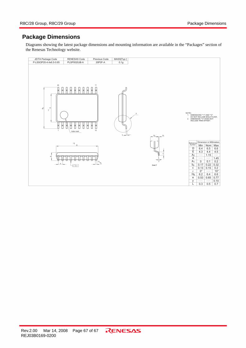
Rev.2.00 Mar 14, 2008 Page 67 of 67REJ03B0169-0200
R8C/28 Group, R8C/29 Group Package Dimensions
Package DimensionsDiagrams showing the latest package dimensions and mounting information are available in the “Packages” section ofthe Renesas Technology website.
y
Index mark1 10
1120
F
*1
*3
*2
c
bpe
A
D
E
HE
INCLUDE TRIM OFFSET.DIMENSION "*3" DOES NOT
NOTE)
DO NOT INCLUDE MOLD FLASH.DIMENSIONS "*1" AND "*2"1.
2.
Detail F
A1A2
L
0.320.220.17bp
Previous CodeJEITA Package Code RENESAS Code
PLSP0020JB-A 20P2F-A
MASS[Typ.]
0.1gP-LSSOP20-4.4x6.5-0.65
0.20.150.13
MaxNomMin
Dimension in Millimeters
SymbolReference
6.66.56.4D
4.54.44.3E
1.15A2
6.66.46.2
1.45A
0.20.10
0.70.50.3L
10°0°
c
0.65e
0.10y
HE
A1
0.53 0.77
A - 1
REVISION HISTORY R8C/28 Group, R8C/29 Group Datasheet
Rev. DateDescription
Page Summary0.10 Nov 14, 2005 − First Edition issued0.30 Feb 28, 2006 all pages “J, K version” added
1 1.1 Applications revised2 Table 1.1 Functions and Specifications for R8C/28 Group revised3 Table 1.2 Functions and Specifications for R8C/29 Group revised4 Figure 1.1 Block Diagram; NOTE3 added5 Table 1.3 Product Information for R8C/28 Group and Figure 1.2 Type
Number, Memory Size, and Package of R8C/28 Group revised6 Table 1.4 Product Information for R8C/29 Group and Figure 1.3 Type
Number, Memory Size, and Package of R8C/29 Group revised7 Figure 1.4 Pin Assignments (Top View); NOTE3 added8 Table 1.5 Pin Functions revised9 Table 1.6 Pin Name Information by Pin Number;
“XOUT” → “XOUT/XCOUT”, “XIN” → “XIN/XCIN” revised and NOTE2 added
13 Figure 3.1 Memory Map of R8C/28 Group; “R5F21284JSP, R5F21284KSP” added
14 Figure 3.2 Memory Map of R8C/29 Group;“R5F21294JSP, R5F21294KSP” added
15 Table 4.1 SFR Information (1); NOTE6 added18 Table 4.4 SFR Information (4);
00FEh: “DRR” → “P1DRR” symbol name revised22 to 66 5. Electrical Characteristics added
0.40 Mar 29, 2006 2 Table 1.1 Functions and Specifications for R8C/28 Group revised3 Table 1.2 Functions and Specifications for R8C/29 Group revised15 Table 4.1 SFR Information (1);
- 0032h, 0036h, 0038h revised- NOTES 2 to 6 revised and NOTES 7 to 8 added
19 Table 4.5 SFR Information (5); NOTE2 added0.50 Apr 27, 2006 18 Table 4.4; 00FDh: revised
46 Table 5.35; System clock Conditions: revised1.00 Nov 08, 2006 All pages “PRELIMINARY” deleted
1 1 “J and K versions are under development...notice.” added2 Table 1.1 revised3 Table 1.2 revised4 Figure 1.1 revised5 Table 1.3 revised6 Table 1.4 revised
REVISION HISTORY R8C/28 Group, R8C/29 Group Datasheet
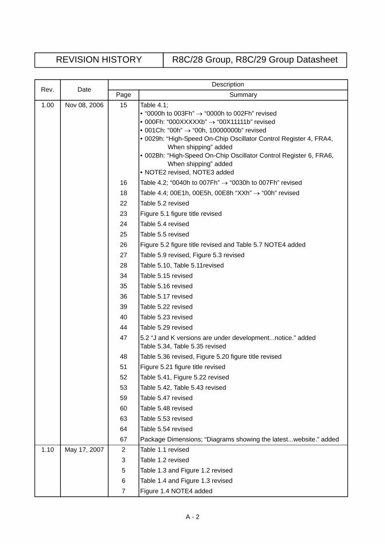
A - 2
REVISION HISTORY R8C/28 Group, R8C/29 Group Datasheet
1.00 Nov 08, 2006 15 Table 4.1;• “0000h to 003Fh” → “0000h to 002Fh” revised• 000Fh: “000XXXXXb” → “00X11111b” revised• 001Ch: “00h” → “00h, 10000000b” revised• 0029h: “High-Speed On-Chip Oscillator Control Register 4, FRA4,
When shipping” added• 002Bh: “High-Speed On-Chip Oscillator Control Register 6, FRA6,
When shipping” added• NOTE2 revised, NOTE3 added
16 Table 4.2; “0040h to 007Fh” → “0030h to 007Fh” revised18 Table 4.4; 00E1h, 00E5h, 00E8h “XXh” → “00h” revised22 Table 5.2 revised23 Figure 5.1 figure title revised24 Table 5.4 revised25 Table 5.5 revised26 Figure 5.2 figure title revised and Table 5.7 NOTE4 added27 Table 5.9 revised, Figure 5.3 revised28 Table 5.10, Table 5.11revised34 Table 5.15 revised35 Table 5.16 revised36 Table 5.17 revised39 Table 5.22 revised40 Table 5.23 revised44 Table 5.29 revised47 5.2 “J and K versions are under development...notice.” added
Table 5.34, Table 5.35 revised48 Table 5.36 revised, Figure 5.20 figure title revised51 Figure 5.21 figure title revised52 Table 5.41, Figure 5.22 revised53 Table 5.42, Table 5.43 revised59 Table 5.47 revised60 Table 5.48 revised63 Table 5.53 revised64 Table 5.54 revised67 Package Dimensions; “Diagrams showing the latest...website.” added
1.10 May 17, 2007 2 Table 1.1 revised3 Table 1.2 revised5 Table 1.3 and Figure 1.2 revised6 Table 1.4 and Figure 1.3 revised7 Figure 1.4 NOTE4 added
Rev. DateDescription
Page Summary
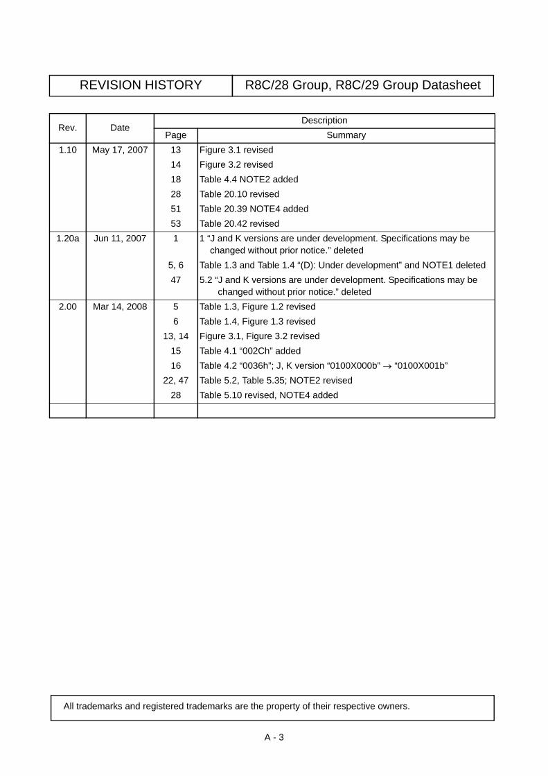
A - 3
REVISION HISTORY R8C/28 Group, R8C/29 Group Datasheet
1.10 May 17, 2007 13 Figure 3.1 revised14 Figure 3.2 revised18 Table 4.4 NOTE2 added28 Table 20.10 revised51 Table 20.39 NOTE4 added53 Table 20.42 revised
1.20a Jun 11, 2007 1 1 “J and K versions are under development. Specifications may be changed without prior notice.” deleted
5, 6 Table 1.3 and Table 1.4 “(D): Under development” and NOTE1 deleted47 5.2 “J and K versions are under development. Specifications may be
changed without prior notice.” deleted2.00 Mar 14, 2008 5 Table 1.3, Figure 1.2 revised
6 Table 1.4, Figure 1.3 revised13, 14 Figure 3.1, Figure 3.2 revised
15 Table 4.1 “002Ch” added16 Table 4.2 “0036h”; J, K version “0100X000b” → “0100X001b”
22, 47 Table 5.2, Table 5.35; NOTE2 revised28 Table 5.10 revised, NOTE4 added
Rev. DateDescription
Page Summary
All trademarks and registered trademarks are the property of their respective owners.

Notes:1. This document is provided for reference purposes only so that Renesas customers may select the appropriate Renesas products for their use. Renesas neither makes warranties or representations with respect to the accuracy or completeness of the information contained in this document nor grants any license to any intellectual property rights or any other rights of Renesas or any third party with respect to the information in this document. 2. Renesas shall have no liability for damages or infringement of any intellectual property or other rights arising out of the use of any information in this document, including, but not limited to, product data, diagrams, charts, programs, algorithms, and application circuit examples.3. You should not use the products or the technology described in this document for the purpose of military applications such as the development of weapons of mass destruction or for the purpose of any other military use. When exporting the products or technology described herein, you should follow the applicable export control laws and regulations, and procedures required by such laws and regulations.4. All information included in this document such as product data, diagrams, charts, programs, algorithms, and application circuit examples, is current as of the date this document is issued. Such information, however, is subject to change without any prior notice. Before purchasing or using any Renesas products listed in this document, please confirm the latest product information with a Renesas sales office. Also, please pay regular and careful attention to additional and different information to be disclosed by Renesas such as that disclosed through our website. (http://www.renesas.com )5. Renesas has used reasonable care in compiling the information included in this document, but Renesas assumes no liability whatsoever for any damages incurred as a result of errors or omissions in the information included in this document.6. When using or otherwise relying on the information in this document, you should evaluate the information in light of the total system before deciding about the applicability of such information to the intended application. Renesas makes no representations, warranties or guaranties regarding the suitability of its products for any particular application and specifically disclaims any liability arising out of the application and use of the information in this document or Renesas products. 7. With the exception of products specified by Renesas as suitable for automobile applications, Renesas products are not designed, manufactured or tested for applications or otherwise in systems the failure or malfunction of which may cause a direct threat to human life or create a risk of human injury or which require especially high quality and reliability such as safety systems, or equipment or systems for transportation and traffic, healthcare, combustion control, aerospace and aeronautics, nuclear power, or undersea communication transmission. If you are considering the use of our products for such purposes, please contact a Renesas sales office beforehand. Renesas shall have no liability for damages arising out of the uses set forth above.8. Notwithstanding the preceding paragraph, you should not use Renesas products for the purposes listed below: (1) artificial life support devices or systems (2) surgical implantations (3) healthcare intervention (e.g., excision, administration of medication, etc.) (4) any other purposes that pose a direct threat to human life Renesas shall have no liability for damages arising out of the uses set forth in the above and purchasers who elect to use Renesas products in any of the foregoing applications shall indemnify and hold harmless Renesas Technology Corp., its affiliated companies and their officers, directors, and employees against any and all damages arising out of such applications. 9. You should use the products described herein within the range specified by Renesas, especially with respect to the maximum rating, operating supply voltage range, movement power voltage range, heat radiation characteristics, installation and other product characteristics. Renesas shall have no liability for malfunctions or damages arising out of the use of Renesas products beyond such specified ranges.10. Although Renesas endeavors to improve the quality and reliability of its products, IC products have specific characteristics such as the occurrence of failure at a certain rate and malfunctions under certain use conditions. Please be sure to implement safety measures to guard against the possibility of physical injury, and injury or damage caused by fire in the event of the failure of a Renesas product, such as safety design for hardware and software including but not limited to redundancy, fire control and malfunction prevention, appropriate treatment for aging degradation or any other applicable measures. Among others, since the evaluation of microcomputer software alone is very difficult, please evaluate the safety of the final products or system manufactured by you. 11. In case Renesas products listed in this document are detached from the products to which the Renesas products are attached or affixed, the risk of accident such as swallowing by infants and small children is very high. You should implement safety measures so that Renesas products may not be easily detached from your products. Renesas shall have no liability for damages arising out of such detachment.12. This document may not be reproduced or duplicated, in any form, in whole or in part, without prior written approval from Renesas. 13. Please contact a Renesas sales office if you have any questions regarding the information contained in this document, Renesas semiconductor products, or if you have any other inquiries.
Sales Strategic Planning Div. Nippon Bldg., 2-6-2, Ohte-machi, Chiyoda-ku, Tokyo 100-0004, Japan
http://www.renesas.comRefer to "http://www.renesas.com/en/network" for the latest and detailed information.
Renesas Technology America, Inc.450 Holger Way, San Jose, CA 95134-1368, U.S.ATel: <1> (408) 382-7500, Fax: <1> (408) 382-7501 Renesas Technology Europe LimitedDukes Meadow, Millboard Road, Bourne End, Buckinghamshire, SL8 5FH, U.K.Tel: <44> (1628) 585-100, Fax: <44> (1628) 585-900
Renesas Technology (Shanghai) Co., Ltd.Unit 204, 205, AZIACenter, No.1233 Lujiazui Ring Rd, Pudong District, Shanghai, China 200120Tel: <86> (21) 5877-1818, Fax: <86> (21) 6887-7858/7898 Renesas Technology Hong Kong Ltd.7th Floor, North Tower, World Finance Centre, Harbour City, Canton Road, Tsimshatsui, Kowloon, Hong Kong Tel: <852> 2265-6688, Fax: <852> 2377-3473
Renesas Technology Taiwan Co., Ltd.10th Floor, No.99, Fushing North Road, Taipei, TaiwanTel: <886> (2) 2715-2888, Fax: <886> (2) 3518-3399 Renesas Technology Singapore Pte. Ltd.1 Harbour Front Avenue, #06-10, Keppel Bay Tower, Singapore 098632 Tel: <65> 6213-0200, Fax: <65> 6278-8001
Renesas Technology Korea Co., Ltd.Kukje Center Bldg. 18th Fl., 191, 2-ka, Hangang-ro, Yongsan-ku, Seoul 140-702, KoreaTel: <82> (2) 796-3115, Fax: <82> (2) 796-2145 Renesas Technology Malaysia Sdn. BhdUnit 906, Block B, Menara Amcorp, Amcorp Trade Centre, No.18, Jln Persiaran Barat, 46050 Petaling Jaya, Selangor Darul Ehsan, MalaysiaTel: <603> 7955-9390, Fax: <603> 7955-9510
RENESAS SALES OFFICES
© 2008. Renesas Technology Corp., All rights reserved. Printed in Japan.
Colophon .7.2