Embed Size (px)
Citation preview

Quartus II Introduction Using VHDL Design
This tutorial presents an introduction to the QuartusR© II CAD system. It gives a general overview of a typi-cal CAD flow for designing circuits that are implemented by using FPGA devices, and shows how this flow isrealized in the Quartus II software. The design process is illustrated by giving step-by-step instructions for usingthe Quartus II software to implement a very simple circuit inan Altera FPGA device.
The Quartus II system includes full support for all of the popular methods of entering a description of thedesired circuit into a CAD system. This tutorial makes use ofthe VHDL design entry method, in which the userspecifies the desired circuit in the VHDL hardware description language. Two other versions of this tutorial arealso available; one uses the Verilog hardware description language and the other is based on defining the desiredcircuit in the form of a schematic diagram.
The last step in the design process involves configuring the designed circuit in an actual FPGA device. Toshow how this is done, it is assumed that the user has access tothe Altera DE2 Development and Education boardconnected to a computer that has Quartus II software installed. A reader who does not have access to the DE2board will still find the tutorial useful to learn how the FPGAprogramming and configuration task is performed.
The screen captures in the tutorial were obtained using the Quartus II version 5.0; if other versions of thesoftware are used, some of the images may be slightly different.
Contents:Typical CAD flowGetting startedStarting a New ProjectVHDL Design EntryCompiling the DesignPin AssignmentSimulating the Designed CircuitProgramming and Configuring the FPGA DeviceTesting the Designed Circuit
1

Computer Aided Design (CAD) software makes it easy to implement a desired logic circuit by using a pro-grammable logic device, such as a field-programmable gate array (FPGA) chip. A typical FPGA CAD flow isillustrated in Figure 1.
Design correct?
Functional Simulation
No
Yes
Synthesis
Timing requirements met?
Fitting
Timing Analysis and Simulation
Programming and Configuration
Yes
No
Design Entry
Figure 1. Typical CAD flow.
The CAD flow involves the following steps:
• Design Entry – the desired circuit is specified either by means of a schematic diagram, or by using ahardware description language, such as VHDL or Verilog
• Synthesis– the entered design is synthesized into a circuit that consists of the logic elements (LEs) providedin the FPGA chip
• Functional Simulation – the synthesized circuit is tested to verify its functionalcorrectness; this simulationdoes not take into account any timing issues
2
• Fitting – the CAD Fitter tool determines the placement of the LEs defined in the netlist into the LEs inan actual FPGA chip; it also chooses routing wires in the chipto make the required connections betweenspecific LEs
• Timing Analysis – propagation delays along the various paths in the fitted circuit are analyzed to providean indication of the expected performance of the circuit
• Timing Simulation – the fitted circuit is tested to verify both its functional correctness and timing
• Programming and Configuration – the designed circuit is implemented in a physical FPGA chipby pro-gramming the configuration switches that configure the LEs and establish the required wiring connections
This tutorial introduces the basic features of the Quartus II software. It shows how the software can be used todesign and implement a circuit specified by using the VHDL hardware description language. It makes use of thegraphical user interface to invoke the Quartus II commands.Doing this tutorial, the reader will learn about:
• Creating a project
• Design entry using VHDL code
• Synthesizing a circuit specified in VHDL code
• Fitting a synthesized circuit into an Altera FPGA
• Assigning the circuit inputs and outputs to specific pins on the FPGA
• Simulating the designed circuit
• Programming and configuring the FPGA chip on Altera’s DE2 board
1 Getting Started
Each logic circuit, or subcircuit, being designed with Quartus II software is called aproject. The software workson one project at a time and keeps all information for that project in a single directory (folder) in the file system.To begin a new logic circuit design, the first step is to createa directory to hold its files. To hold the design filesfor this tutorial, we will use a directoryintrotutorial. The running example for this tutorial is a simple circuit fortwo-way light control.
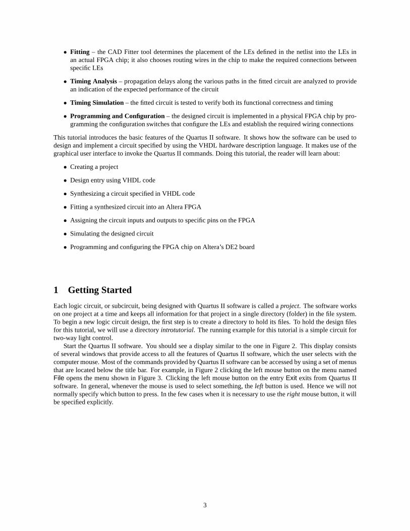
Start the Quartus II software. You should see a display similar to the one in Figure 2. This display consistsof several windows that provide access to all the features ofQuartus II software, which the user selects with thecomputer mouse. Most of the commands provided by Quartus II software can be accessed by using a set of menusthat are located below the title bar. For example, in Figure 2clicking the left mouse button on the menu namedFile opens the menu shown in Figure 3. Clicking the left mouse button on the entryExit exits from Quartus IIsoftware. In general, whenever the mouse is used to select something, theleft button is used. Hence we will notnormally specify which button to press. In the few cases whenit is necessary to use theright mouse button, it willbe specified explicitly.
3
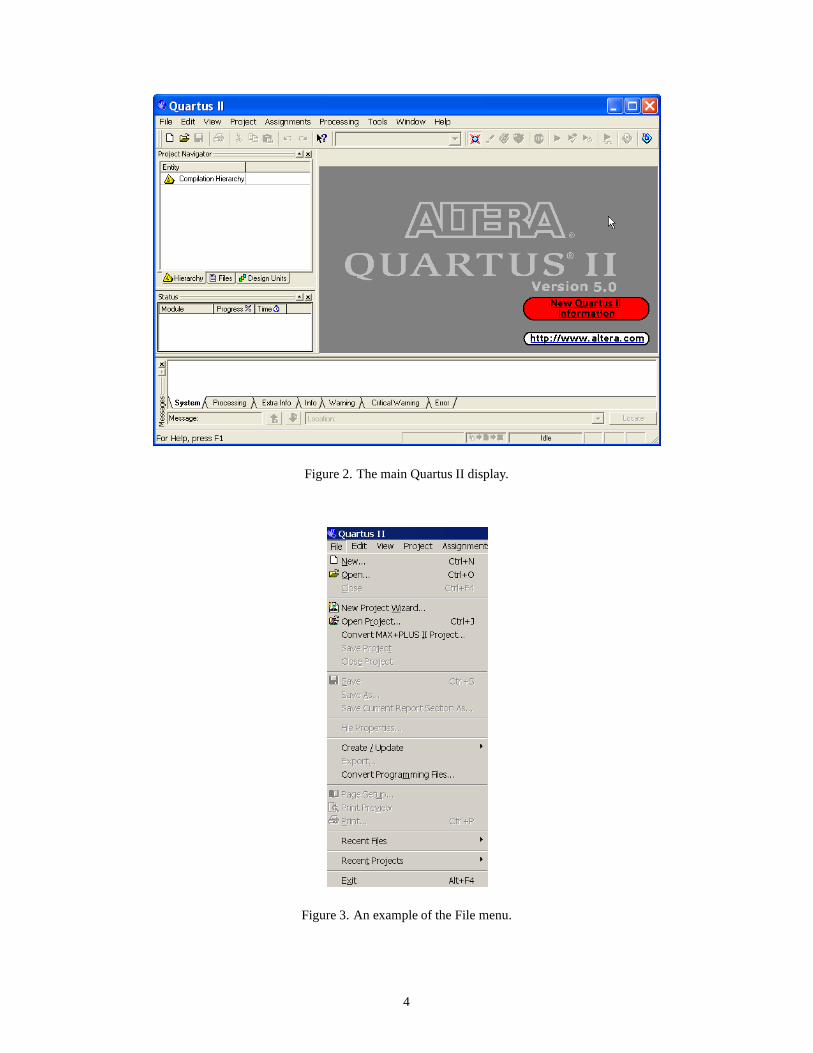
Figure 2. The main Quartus II display.
Figure 3. An example of the File menu.
4
For some commands it is necessary to access two or more menus in sequence. We use the conventionMenu1> Menu2 > Item to indicate that to select the desired command the user should first click the left mouse buttonon Menu1, then within this menu click onMenu2, and then withinMenu2 click on Item. For example,File >
Exit uses the mouse to exit from the system. Many commands can be invoked by clicking on an icon displayed inone of the toolbars. To see the command associated with an icon, position the mouse over the icon and a tooltipwill appear that displays the command name.
1.1 Quartus II Online Help
Quartus II software provides comprehensive online documentation that answers many of the questions that mayarise when using the software. The documentation is accessed from the menu in theHelp window. To get someidea of the extent of documentation provided, it is worthwhile for the reader to browse through theHelp menu.For instance, selectingHelp > How to Use Help gives an indication of what type of help is provided.
The user can quickly search through the Help topics by selecting Help > Search, which opens a dialog boxinto which key words can be entered. Another method, context-sensitive help, is provided for quickly findingdocumentation for specific topics. While using most applications, pressing theF1 function key on the keyboardopens a Help display that shows the commands available for the application.
2 Starting a New Project
To start working on a new design we first have to define a newdesign project. Quartus II software makes thedesigner’s task easy by providing support in the form of awizard. Create a new project as follows:
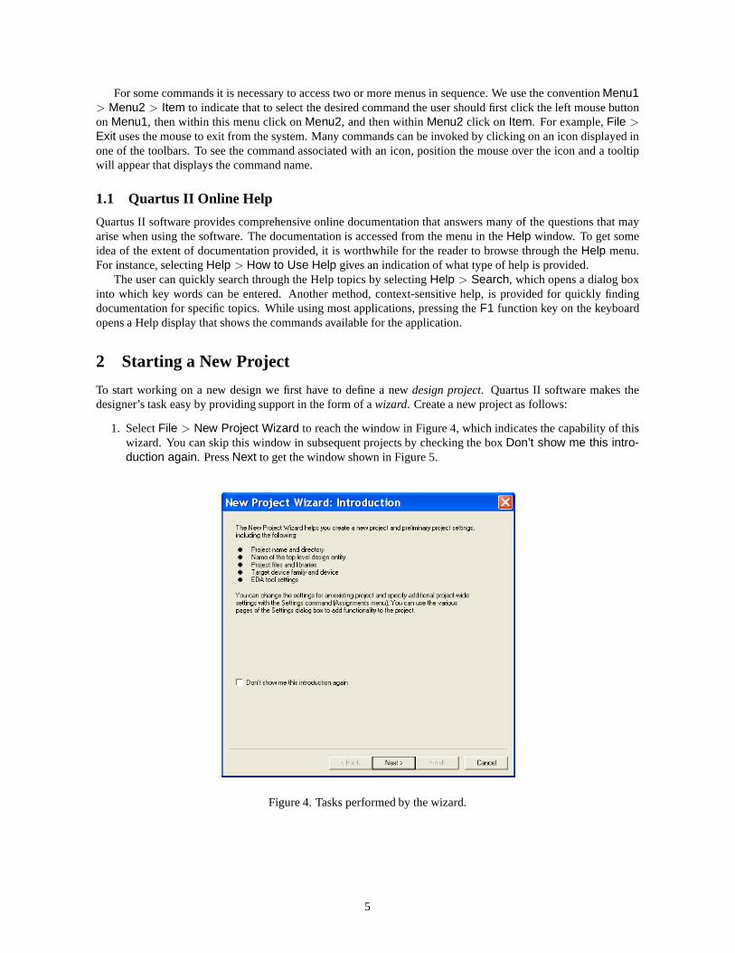
1. SelectFile > New Project Wizard to reach the window in Figure 4, which indicates the capability of thiswizard. You can skip this window in subsequent projects by checking the boxDon’t show me this intro-duction again. PressNext to get the window shown in Figure 5.
Figure 4. Tasks performed by the wizard.
5
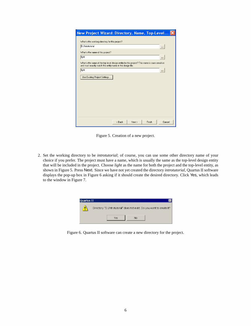
Figure 5. Creation of a new project.
2. Set the working directory to beintrotutorial; of course, you can use some other directory name of yourchoice if you prefer. The project must have a name, which is usually the same as the top-level design entitythat will be included in the project. Chooselight as the name for both the project and the top-level entity, asshown in Figure 5. PressNext. Since we have not yet created the directoryintrotutorial, Quartus II softwaredisplays the pop-up box in Figure 6 asking if it should createthe desired directory. ClickYes, which leadsto the window in Figure 7.
Figure 6. Quartus II software can create a new directory for the project.
6

Figure 7. The wizard can include user-specified design files.
3. The wizard makes it easy to specify which existing files (ifany) should be included in the project. Assumingthat we do not have any existing files, clickNext, which leads to the window in Figure 8.
Figure 8. Choose the device family and a specific device.
7
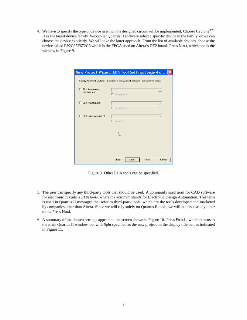
4. We have to specify the type of device in which the designed circuit will be implemented. Choose CycloneTM
II as the target device family. We can let Quartus II softwareselect a specific device in the family, or we canchoose the device explicitly. We will take the latter approach. From the list of available devices, choose thedevice called EP2C35F672C6 which is the FPGA used on Altera’s DE2 board. PressNext, which opens thewindow in Figure 9.
Figure 9. Other EDA tools can be specified.
5. The user can specify any third-party tools that should be used. A commonly used term for CAD softwarefor electronic circuits isEDA tools, where the acronym stands for Electronic Design Automation. This termis used in Quartus II messages that refer to third-party tools, which are the tools developed and marketedby companies other than Altera. Since we will rely solely on Quartus II tools, we will not choose any othertools. PressNext.
6. A summary of the chosen settings appears in the screen shown in Figure 10. PressFinish, which returns tothe main Quartus II window, but withlight specified as the new project, in the display title bar, as indicatedin Figure 11.
8
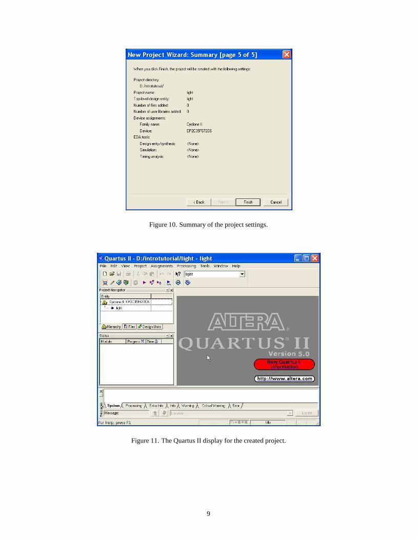
Figure 10. Summary of the project settings.
Figure 11. The Quartus II display for the created project.
9

3 Design Entry Using VHDL Code
As a design example, we will use the two-way light controllercircuit shown in Figure 12. The circuit can be usedto control a single light from either of the two switches,x1 andx2, where a closed switch corresponds to the logicvalue 1. The truth table for the circuit is also given in the figure. Note that this is just the Exclusive-OR functionof the inputsx1 andx2, but we will specify it using the gates shown.
f
x1
x2
x1 x2
0 0
10
01
1 1
f
0
1
1
0
Figure 12. The light controller circuit.
The required circuit is described by the VHDL code in Figure 13. Note that the VHDL entity is calledlight tomatch the name given in Figure 5, which was specified when the project was created. This code can be typed intoa file by using any text editor that stores ASCII files, or by using the Quartus II text editing facilities. While thefile can be given any name, it is a common designers’ practice to use the same name as the name of the top-levelVHDL entity. The file name must include the extensionvhd, which indicates a VHDL file. So, we will use thenamelight.vhd.
LIBRARY ieee ;USE ieee.stdlogic 1164.all ;ENTITY light IS
PORT ( x1, x2 : IN STDLOGIC ;f : OUT STD LOGIC ) ;
END light ;
ARCHITECTURE LogicFunction OF light ISBEGIN
f <= (x1 AND NOT x2) OR (NOT x1 AND x2);END LogicFunction ;
Figure 13. VHDL code for the circuit in Figure 12.
3.1 Using the Quartus II Text Editor
This section shows how to use the Quartus II Text Editor. You can skip this section if you prefer to use some othertext editor to create the VHDL source code file, which we will namelight.vhd.
SelectFile > New to get the window in Figure 14, chooseVHDL File, and clickOK. This opens the TextEditor window. The first step is to specify a name for the file that will be created. SelectFile > Save As to openthe pop-up box depicted in Figure 15. In the box labeledSave as type chooseVHDL File. In the box labeledFile name type light. Put a checkmark in the boxAdd file to current project. Click Save, which puts the fileinto the directoryintrotutorial and leads to the Text Editor window shown in Figure 16. Maximize the Text Editor
10
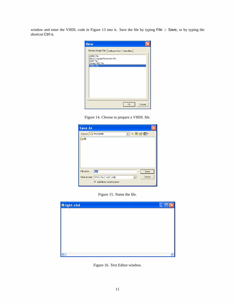
window and enter the VHDL code in Figure 13 into it. Save the file by typingFile > Save, or by typing theshortcutCtrl-s.
Figure 14. Choose to prepare a VHDL file.
Figure 15. Name the file.
Figure 16. Text Editor window.
11
Most of the commands available in the Text Editor are self-explanatory. Text is entered at theinsertion point,which is indicated by a thin vertical line. The insertion point can be moved either by using the keyboard arrowkeys or by using the mouse. Two features of the Text Editor areespecially convenient for typing VHDL code.First, the editor can display different types of VHDL statements in different colors, which is the default choice.Second, the editor can automatically indent the text on a newline so that it matches the previous line. Such optionscan be controlled by the settings inTools > Options > Text Editor.
3.1.1 Using VHDL Templates
The syntax of VHDL code is sometimes difficult for a designer to remember. To help with this issue, the TextEditor provides a collection ofVHDL templates. The templates provide examples of various types of VHDLstatements, such as an ENTITY declaration, a CASE statement, and assignment statements. It is worthwhileto browse through the templates by selectingEdit > Insert Template > VHDL to become familiar with thisresource.
3.2 Adding Design Files to a Project
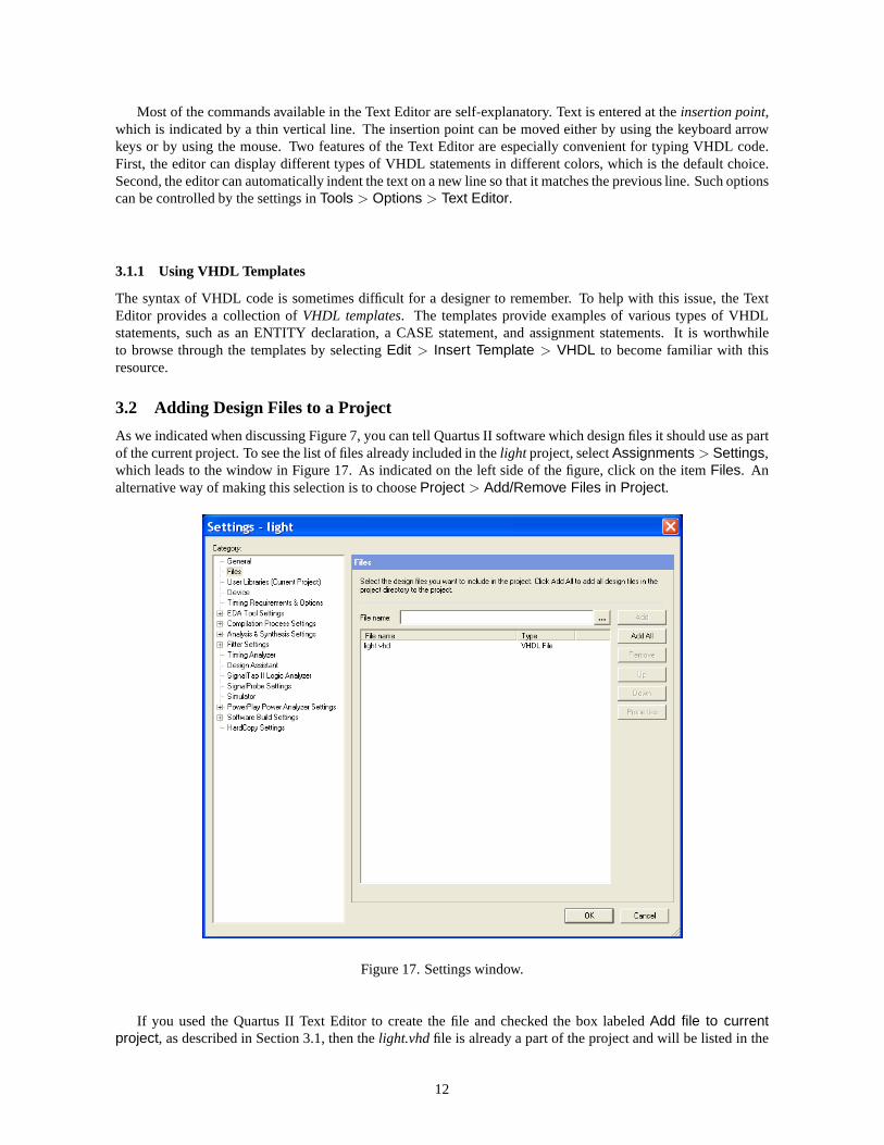
As we indicated when discussing Figure 7, you can tell Quartus II software which design files it should use as partof the current project. To see the list of files already included in thelight project, selectAssignments > Settings,which leads to the window in Figure 17. As indicated on the left side of the figure, click on the itemFiles. Analternative way of making this selection is to chooseProject > Add/Remove Files in Project.
Figure 17. Settings window.
If you used the Quartus II Text Editor to create the file and checked the box labeledAdd file to currentproject, as described in Section 3.1, then thelight.vhdfile is already a part of the project and will be listed in the
12
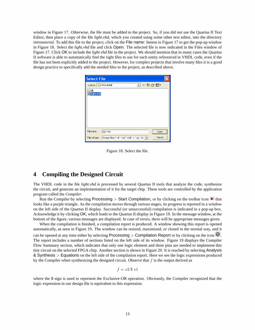
window in Figure 17. Otherwise, the file must be added to the project. So, if you did not use the Quartus II TextEditor, then place a copy of the filelight.vhd, which you created using some other text editor, into the directoryintrotutorial. To add this file to the project, click on theFile name: button in Figure 17 to get the pop-up windowin Figure 18. Select thelight.vhdfile and clickOpen. The selected file is now indicated in the Files window ofFigure 17. ClickOK to include thelight.vhdfile in the project. We should mention that in many cases the QuartusII software is able to automatically find the right files to usefor each entity referenced in VHDL code, even if thefile has not been explicitly added to the project. However, for complex projects that involve many files it is a gooddesign practice to specifically add the needed files to the project, as described above.
Figure 18. Select the file.
4 Compiling the Designed Circuit
The VHDL code in the filelight.vhd is processed by several Quartus II tools that analyze the code, synthesizethe circuit, and generate an implementation of it for the target chip. These tools are controlled by the applicationprogram called theCompiler.
Run the Compiler by selectingProcessing > Start Compilation, or by clicking on the toolbar icon thatlooks like a purple triangle. As the compilation moves through various stages, its progress is reported in a windowon the left side of the Quartus II display. Successful (or unsuccessful) compilation is indicated in a pop-up box.Acknowledge it by clickingOK, which leads to the Quartus II display in Figure 19. In the message window, at thebottom of the figure, various messages are displayed. In caseof errors, there will be appropriate messages given.
When the compilation is finished, a compilation report is produced. A window showing this report is openedautomatically, as seen in Figure 19. The window can be resized, maximized, or closed in the normal way, and it
can be opened at any time either by selectingProcessing > Compilation Report or by clicking on the icon .The report includes a number of sections listed on the left side of its window. Figure 19 displays the CompilerFlow Summary section, which indicates that only one logic element and three pins are needed to implement thistiny circuit on the selected FPGA chip. Another section is shown in Figure 20. It is reached by selectingAnalysis& Synthesis > Equations on the left side of the compilation report. Here we see the logic expressions producedby the Compiler when synthesizing the designed circuit. Observe thatf is the output derived as
f = x2 $ x1
where the $ sign is used to represent the Exclusive-OR operation. Obviously, the Compiler recognized that thelogic expression in our design file is equivalent to this expression.
13
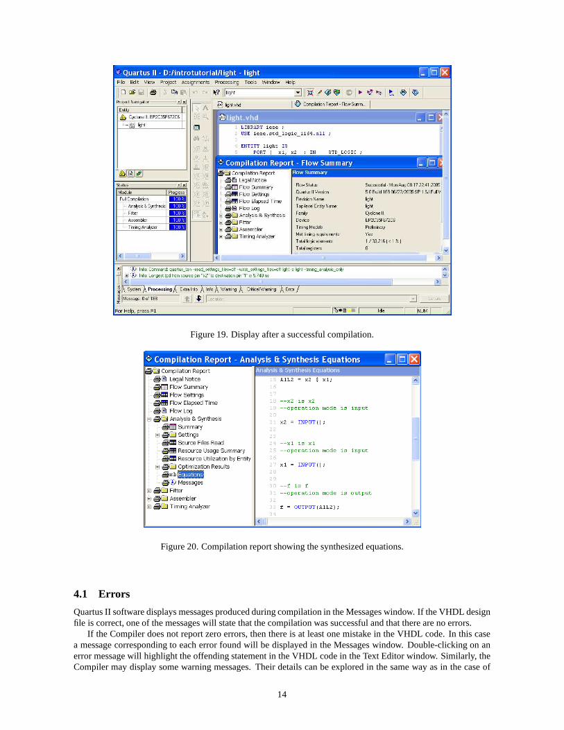
Figure 19. Display after a successful compilation.
Figure 20. Compilation report showing the synthesized equations.
4.1 Errors
Quartus II software displays messages produced during compilation in the Messages window. If the VHDL designfile is correct, one of the messages will state that the compilation was successful and that there are no errors.
If the Compiler does not report zero errors, then there is at least one mistake in the VHDL code. In this casea message corresponding to each error found will be displayed in the Messages window. Double-clicking on anerror message will highlight the offending statement in theVHDL code in the Text Editor window. Similarly, theCompiler may display some warning messages. Their details can be explored in the same way as in the case of
14
error messages. The user can obtain more information about aspecific error or warning message by selecting themessage and pressing theF1 function key.
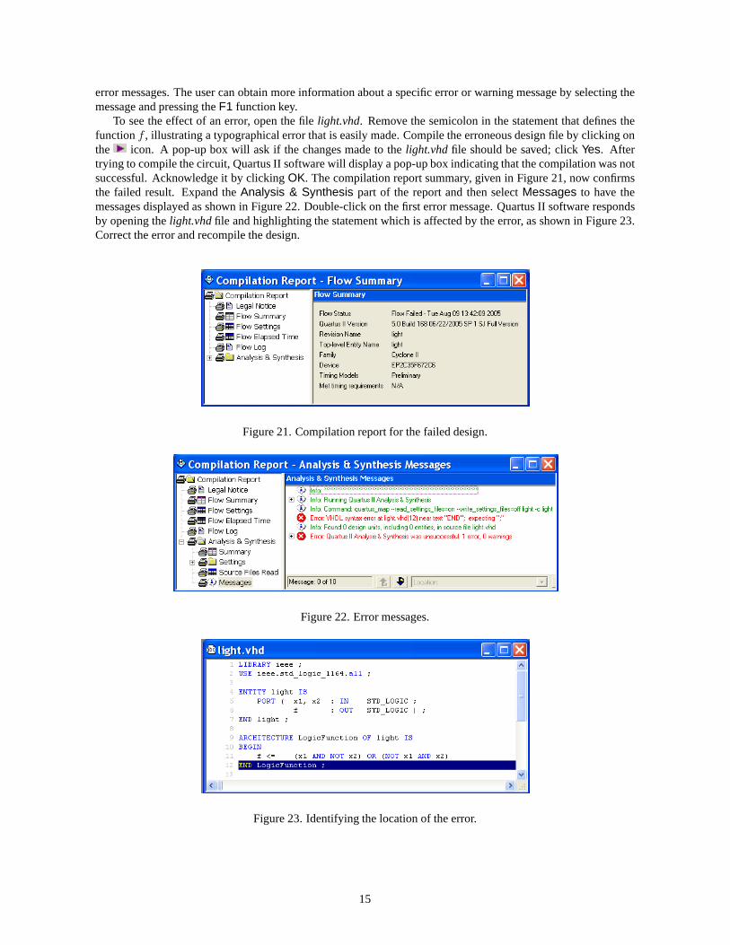
To see the effect of an error, open the filelight.vhd. Remove the semicolon in the statement that defines thefunctionf , illustrating a typographical error that is easily made. Compile the erroneous design file by clicking onthe icon. A pop-up box will ask if the changes made to thelight.vhdfile should be saved; clickYes. Aftertrying to compile the circuit, Quartus II software will display a pop-up box indicating that the compilation was notsuccessful. Acknowledge it by clickingOK. The compilation report summary, given in Figure 21, now confirmsthe failed result. Expand theAnalysis & Synthesis part of the report and then selectMessages to have themessages displayed as shown in Figure 22. Double-click on the first error message. Quartus II software respondsby opening thelight.vhdfile and highlighting the statement which is affected by the error, as shown in Figure 23.Correct the error and recompile the design.
Figure 21. Compilation report for the failed design.
Figure 22. Error messages.
Figure 23. Identifying the location of the error.
15

5 Pin Assignment
During the compilation above, the Quartus II Compiler was free to choose any pins on the selected FPGA to serveas inputs and outputs. However, the DE2 board has hardwired connections between the FPGA pins and the othercomponents on the board. We will use two toggle switches, labeledSW1 andSW0, to provide the external inputs,x1 andx2, to our example circuit. These switches are connected to theFPGA pins N26 and N25, respectively. Wewill connect the outputf to the green light-emitting diode labeledLEDG0, which is hardwired to the FPGA pinAE22.
Pin assignments are made by using the Assignment Editor. SelectAssignments > Pins to reach the windowin Figure 24. UnderCategory selectPin. Double-click on the entry<<new>> which is highlighted in blue inthe column labeled To. The drop-down menu in Figure 25 will appear. Click onx1 as the first pin to be assigned;this will enterx1 in the displayed table. Follow this by double-clicking on the box to the right of this newx1
entry, in the column labeled Location. Now, the drop-down menu in Figure 26 appears. Scroll down and selectPin N26. Instead of scrolling down the menu to find the desired pin, you can just type the name of the pin in theLocation box. Use the same procedure to assign inputx2 to pin N25 and outputf to pin AE22, which resultsin the image in Figure 27. To save the assignments made, choose File > Save. You can also simply close theAssignment Editor window, in which case a pop-up box will askif you want to save the changes to assignments;click Yes. Recompile the circuit, so that it will be compiled with the correct pin assignments.
Figure 24. The Assignment Editor window.
Figure 25. The drop-down menu displays the input and output names.
16
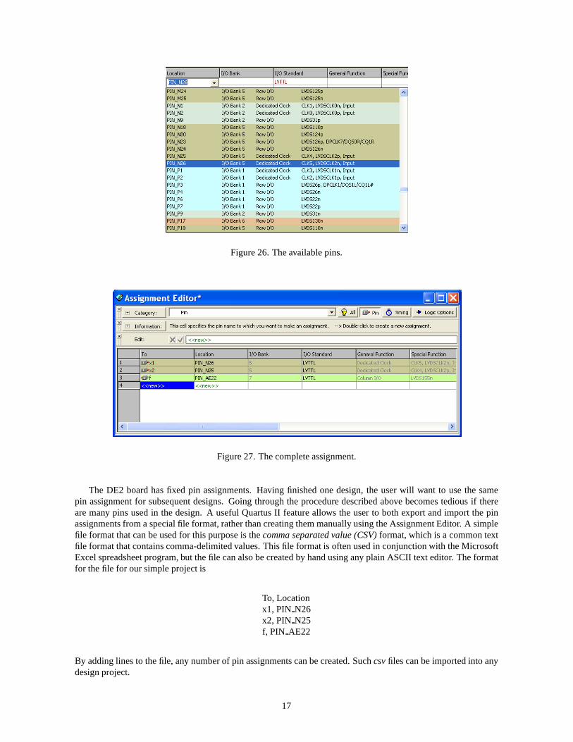
Figure 26. The available pins.
Figure 27. The complete assignment.
The DE2 board has fixed pin assignments. Having finished one design, the user will want to use the samepin assignment for subsequent designs. Going through the procedure described above becomes tedious if thereare many pins used in the design. A useful Quartus II feature allows the user to both export and import the pinassignments from a special file format, rather than creatingthem manually using the Assignment Editor. A simplefile format that can be used for this purpose is thecomma separated value (CSV)format, which is a common textfile format that contains comma-delimited values. This file format is often used in conjunction with the MicrosoftExcel spreadsheet program, but the file can also be created byhand using any plain ASCII text editor. The formatfor the file for our simple project is
To, Locationx1, PIN N26x2, PIN N25f, PIN AE22
By adding lines to the file, any number of pin assignments can be created. Suchcsvfiles can be imported into anydesign project.
17

If you created a pin assignment for a particular project, youcan export it for use in a different project. To seehow this is done, open again the Assignment Editor to reach the window in Figure 27. Now, selectFile > Exportwhich leads to the window in Figure 28. Here, the filelight.csvis available for export. Click onExport. If younow look in the directoryintrotutorial, you will see that the filelight.csvhas been created.
Figure 28. Exporting the pin assignment.
You can import a pin assignment by choosingAssignments > Import Assignments. This opens the dia-logue in Figure 29 to select the file to import. Type the name ofthe file, including thecsvextension and the fullpath to the directory that holds the file, in the File Name box and pressOK. Of course, you can also browse tofind the desired file. For convenience, all relevant pin assignments for the DE2 board are given in the file calledDE2 pin assignment.csvin the directoryDE2 tutorials\designfiles, which is included on the CD-ROM that ac-companies the DE2 board and can also be found on Altera’s DE2 web pages.
Figure 29. Importing the pin assignment.
6 Simulating the Designed Circuit
Before implementing the designed circuit in the FPGA chip onthe DE2 board, it is prudent to simulate it toascertain its correctness. Quartus II software includes a simulation tool that can be used to simulate the behaviorof a designed circuit. Before the circuit can be simulated, it is necessary to create the desired waveforms, calledtest vectors, to represent the input signals. It is also necessary to specify which outputs, as well as possible internalpoints in the circuit, the designer wishes to observe. The simulator applies the test vectors to a model of theimplemented circuit and determines the expected response.We will use the Quartus II Waveform Editor to drawthe test vectors, as follows:
18
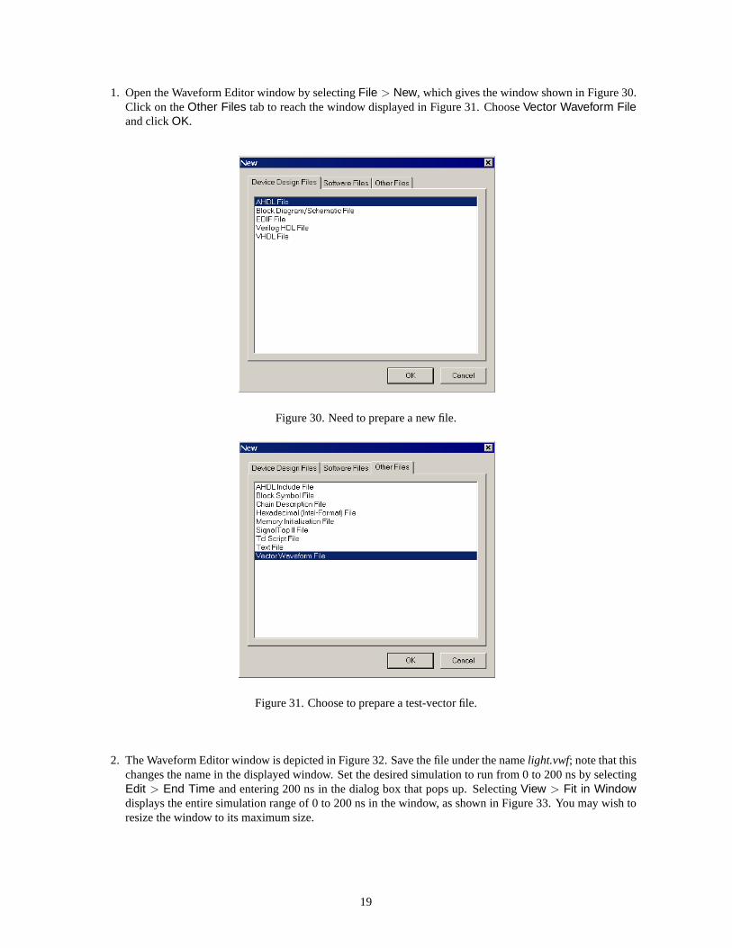
1. Open the Waveform Editor window by selectingFile > New, which gives the window shown in Figure 30.Click on theOther Files tab to reach the window displayed in Figure 31. ChooseVector Waveform Fileand clickOK.
Figure 30. Need to prepare a new file.
Figure 31. Choose to prepare a test-vector file.
2. The Waveform Editor window is depicted in Figure 32. Save the file under the namelight.vwf; note that thischanges the name in the displayed window. Set the desired simulation to run from 0 to 200 ns by selectingEdit > End Time and entering 200 ns in the dialog box that pops up. SelectingView > Fit in Windowdisplays the entire simulation range of 0 to 200 ns in the window, as shown in Figure 33. You may wish toresize the window to its maximum size.
19
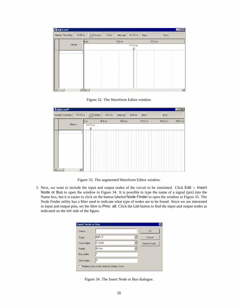
Figure 32. The Waveform Editor window.
Figure 33. The augmented Waveform Editor window.
3. Next, we want to include the input and output nodes of the circuit to be simulated. ClickEdit > InsertNode or Bus to open the window in Figure 34. It is possible to type the nameof a signal (pin) into theName box, but it is easier to click on the button labeledNode Finder to open the window in Figure 35. TheNode Finder utility has a filter used to indicate what type of nodes are to be found. Since we are interestedin input and output pins, set the filter toPins: all. Click theList button to find the input and output nodes asindicated on the left side of the figure.
Figure 34. The Insert Node or Bus dialogue.
20
Figure 35. Selecting nodes to insert into the Waveform Editor.
Click on thex1signal in the Nodes Found box in Figure 35, and then click the> sign to add it to the SelectedNodes box on the right side of the figure. Do the same forx2 and f. Click OK to close the Node Finderwindow, and then clickOK in the window of Figure 34. This leaves a fully displayed Waveform Editorwindow, as shown in Figure 36. If you did not select the nodes in the same order as displayed in Figure 36,it is possible to rearrange them. To move a waveform up or downin the Waveform Editor window, click onthe node name (in the Name column) and release the mouse button. The waveform is now highlighted toshow the selection. Click again on the waveform and drag it upor down in the Waveform Editor.
Figure 36. The nodes needed for simulation.
4. We will now specify the logic values to be used for the inputsignalsx1andx2during simulation. The logicvalues at the outputf will be generated automatically by the simulator. To make iteasy to draw the desiredwaveforms, the Waveform Editor displays (by default) vertical guidelines and provides a drawing featurethat snaps on these lines (which can otherwise be invoked by choosingView > Snap to Grid). Observe alsoa solid vertical line, which can be moved by pointing to its top and dragging it horizontally. This referenceline is used in analyzing the timing of a circuit; move it to the time = 0 position. The waveforms can be
drawn using the Selection Tool, which is activated by selecting the icon in the toolbar, or the Waveform
Editing Tool, which is activated by the icon .
21

To simulate the behavior of a large circuit, it is necessary to apply a sufficient number of input valuations andobserve the expected values of the outputs. In a large circuit the number of possible input valuations maybe huge, so in practice we choose a relatively small (but representative) sample of these input valuations.However, for our tiny circuit we can simulate all four input valuations given in Figure 12. We will use four50-ns time intervals to apply the four test vectors.
We can generate the desired input waveforms as follows. Click on the waveform name for thex1 node.Once a waveform is selected, the editing commands in the Waveform Editor can be used to draw the desiredwaveforms. Commands are available for setting a selected signal to 0, 1, unknown (X), high impedance (Z),don’t care (DC), inverting its existing value (INV), or defining a clock waveform. Each command can beactivated by using theEdit > Value command, or via the toolbar for the Waveform Editor. The Editmenucan also be opened by right-clicking on a waveform name.
Setx1 to 0 in the time interval 0 to 100 ns, which is probably alreadyset by default. Next, setx1 to 1 in thetime interval 100 to 200 ns. Do this by pressing the mouse at the start of the interval and dragging it to itsend, which highlights the selected interval, and choosing the logic value 1 in the toolbar. Makex2= 1 from50 to 100 ns and also from 150 to 200 ns, which corresponds to the truth table in Figure 12. This shouldproduce the image in Figure 37. Observe that the outputf is displayed as having an unknown value at thistime, which is indicated by a hashed pattern; its value will be determined during simulation. Save the file.
Figure 37. Setting of test values.
6.1 Performing the Simulation
A designed circuit can be simulated in two ways. The simplestway is to assume that logic elements and intercon-nection wires in the FPGA are perfect, thus causing no delay in propagation of signals through the circuit. Thisis calledfunctional simulation. A more complex alternative is to take all propagation delays into account, whichleads totiming simulation. Typically, functional simulation is used to verify the functional correctness of a circuitas it is being designed. This takes much less time, because the simulation can be performed simply by using thelogic expressions that define the circuit.
6.1.1 Functional Simulation
To perform the functional simulation, selectAssignments > Settings to open the Settings window. On the leftside of this window click onSimulator to display the window in Figure 38, chooseFunctional as the simulationmode, and clickOK. The Quartus II simulator takes the inputs and generates theoutputs defined in thelight.vwffile. Before running the functional simulation it is necessary to create the required netlist, which is done by se-lectingProcessing > Generate Functional Simulation Netlist. A simulation run is started byProcessing >
Start Simulation, or by using the icon . At the end of the simulation, Quartus II software indicatesits successfulcompletion and displays a Simulation Report illustrated inFigure 39. If your report window does not show theentire simulation time range, click on the report window to select it and chooseView > Fit in Window. Observe
22

that the outputf is as specified in the truth table of Figure 12.
Figure 38. Specifying the simulation mode.
Figure 39. The result of functional simulation.
6.1.2 Timing Simulation
Having ascertained that the designed circuit is functionally correct, we should now perform the timing simulationto see how it will behave when it is actually implemented in the chosen FPGA device. SelectAssignments >
Settings > Simulator to get to the window in Figure 38, chooseTiming as the simulation mode, and clickOK.Run the simulator, which should produce the waveforms in Figure 40. Observe that there is a delay of about 6ns in producing a change in the signalf from the time when the input signals,x1 andx2, change their values.This delay is due to the propagation delays in the logic element and the wires in the FPGA device. You may alsonotice that a momentary change in the value off , from 1 to 0 and back to 1, occurs at about 106-ns point in thesimulation. Thisglitch is also due to the propagation delays in the FPGA device, because changes inx1 andx2
23

may not arrive at exactly the same time at the logic element that generatesf .
Figure 40. The result of timing simulation.
7 Programming and Configuring the FPGA Device
The FPGA device must be programmed and configured to implement the designed circuit. The required configura-tion file is generated by the Quartus II Compiler’s Assemblermodule. Altera’s DE2 board allows the configurationto be done in two different ways, known as JTAG and AS modes. The configuration data is transferred from thehost computer (which runs the Quartus II software) to the board by means of a cable that connects a USB porton the host computer to the leftmost USB connector on the board. To use this connection, it is necessary to havethe USB-Blaster driver installed. If this driver is not already installed, consult the tutorialGetting Started withAltera’s DE2 Boardfor information about installing the driver. Before using the board, make sure that the USBcable is properly connected and turn on the power supply switch on the board.
In the JTAG mode, the configuration data is loaded directly into the FPGA device. The acronym JTAG standsfor Joint Test Action Group. This group defined a simple way for testing digital circuits and loading data intothem, which became an IEEE standard. If the FPGA is configuredin this manner, it will retain its configurationas long as the power remains turned on. The configuration information is lost when the power is turned off. Thesecond possibility is to use the Active Serial (AS) mode. In this case, a configuration device that includes someflash memory is used to store the configuration data. Quartus II software places the configuration data into theconfiguration device on the DE2 board. Then, this data is loaded into the FPGA upon power-up or reconfiguration.Thus, the FPGA need not be configured by the Quartus II software if the power is turned off and on. The choicebetween the two modes is made by the RUN/PROG switch on the DE2board. The RUN position selects the JTAGmode, while the PROG position selects the AS mode.
7.1 JTAG Programming
The programming and configuration task is performed as follows. Flip the RUN/PROG switch into the RUNposition. SelectTools > Programmer to reach the window in Figure 41. Here it is necessary to specify theprogramming hardware and the mode that should be used. If notalready chosen by default, select JTAG in theMode box. Also, if the USB-Blaster is not chosen by default, press theHardware Setup... button and select theUSB-Blaster in the window that pops up, as shown in Figure 42.
24
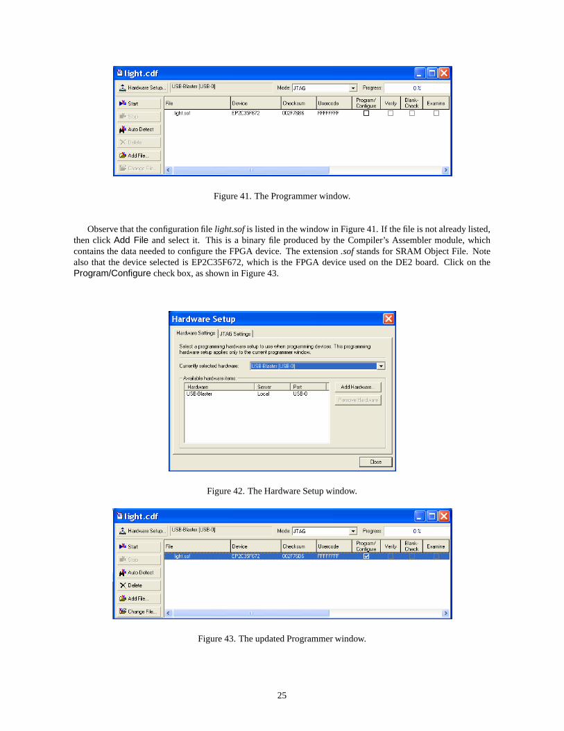
Figure 41. The Programmer window.
Observe that the configuration filelight.sofis listed in the window in Figure 41. If the file is not already listed,then clickAdd File and select it. This is a binary file produced by the Compiler’sAssembler module, whichcontains the data needed to configure the FPGA device. The extension.sofstands for SRAM Object File. Notealso that the device selected is EP2C35F672, which is the FPGA device used on the DE2 board. Click on theProgram/Configure check box, as shown in Figure 43.
Figure 42. The Hardware Setup window.
Figure 43. The updated Programmer window.
25
Now, pressStart in the window in Figure 43. An LED on the board will light up when the configuration datahas been downloaded successfully. If you see an error reported by Quartus II software indicating that programmingfailed, then check to ensure that the board is properly powered on.
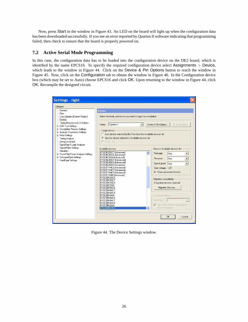
7.2 Active Serial Mode Programming
In this case, the configuration data has to be loaded into the configuration device on the DE2 board, which isidentified by the name EPCS16. To specify the required configuration device selectAssignments > Device,which leads to the window in Figure 44. Click on theDevice & Pin Options button to reach the window inFigure 45. Now, click on theConfiguration tab to obtain the window in Figure 46. In the Configuration devicebox (which may be set to Auto) choose EPCS16 and clickOK. Upon returning to the window in Figure 44, clickOK. Recompile the designed circuit.
Figure 44. The Device Settings window.
26
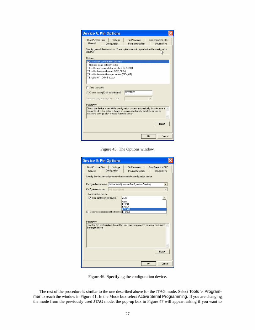
Figure 45. The Options window.
Figure 46. Specifying the configuration device.
The rest of the procedure is similar to the one described above for the JTAG mode. SelectTools > Program-mer to reach the window in Figure 41. In the Mode box selectActive Serial Programming. If you are changingthe mode from the previously used JTAG mode, the pop-up box inFigure 47 will appear, asking if you want to
27
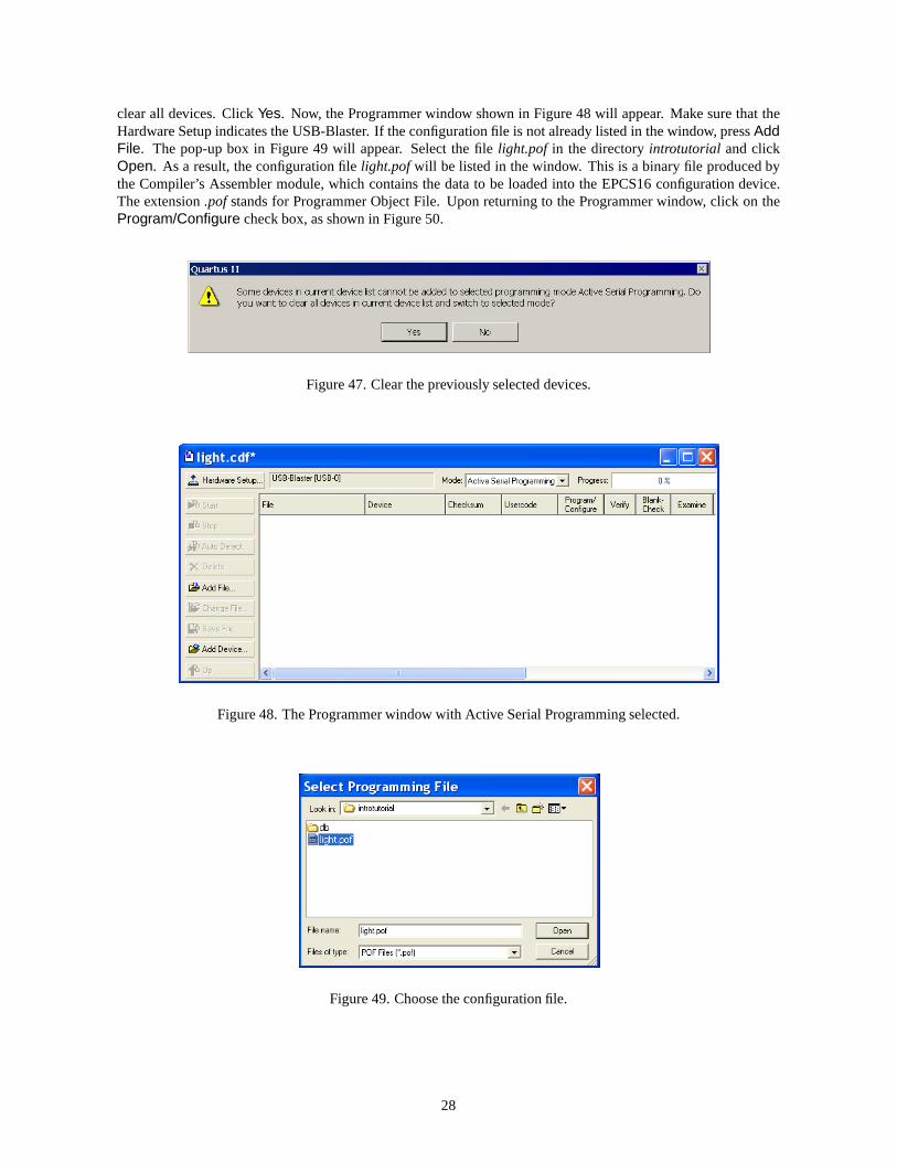
clear all devices. ClickYes. Now, the Programmer window shown in Figure 48 will appear. Make sure that theHardware Setup indicates the USB-Blaster. If the configuration file is not already listed in the window, pressAddFile. The pop-up box in Figure 49 will appear. Select the filelight.pof in the directoryintrotutorial and clickOpen. As a result, the configuration filelight.pofwill be listed in the window. This is a binary file produced bythe Compiler’s Assembler module, which contains the data tobe loaded into the EPCS16 configuration device.The extension.pofstands for Programmer Object File. Upon returning to the Programmer window, click on theProgram/Configure check box, as shown in Figure 50.
Figure 47. Clear the previously selected devices.
Figure 48. The Programmer window with Active Serial Programming selected.
Figure 49. Choose the configuration file.
28

Figure 50. The updated Programmer window.
Flip the RUN/PROG switch on the DE2 board to the PROG position. PressStart in the window in Figure50. An LED on the board will light up when the configuration data has been downloaded successfully. Also, theProgress box in Figure 50 will indicate when the configuration and programming process is completed, as shownin Figure 51.
Figure 51. The Programmer window upon completion of programming.
8 Testing the Designed Circuit
Having downloaded the configuration data into the FPGA device, you can now test the implemented circuit. Flipthe RUN/PROG switch to RUN position. Try all four valuationsof the input variablesx1 andx2, by setting thecorresponding states of the switchesSW1 andSW0. Verify that the circuit implements the truth table in Figure12.
If you want to make changes in the designed circuit, first close the Programmer window. Then make thedesired changes in the VHDL design file, compile the circuit,and program the board as explained above.
29

Copyright c©2005 Altera Corporation. All rights reserved. Altera, The Programmable Solutions Company, thestylized Altera logo, specific device designations, and allother words and logos that are identified as trademarksand/or service marks are, unless noted otherwise, the trademarks and service marks of Altera Corporation inthe U.S. and other countries. All other product or service names are the property of their respective holders.Altera products are protected under numerous U.S. and foreign patents and pending applications, mask workrights, and copyrights. Altera warrants performance of itssemiconductor products to current specifications inaccordance with Altera’s standard warranty, but reserves the right to make changes to any products and services atany time without notice. Altera assumes no responsibility or liability arising out of the application or use of anyinformation, product, or service described herein except as expressly agreed to in writing by Altera Corporation.Altera customers are advised to obtain the latest version ofdevice specifications before relying on any publishedinformation and before placing orders for products or services.This document is being provided on an “as-is” basis and as an accommodation and therefore all warranties, rep-resentations or guarantees of any kind (whether express, implied or statutory) including, without limitation, war-ranties of merchantability, non-infringement, or fitness for a particular purpose, are specifically disclaimed.
30