Embed Size (px)
Citation preview

Quartus II Abbreviated Manual * Creating a new project To start working on a new design we first have to define a new design project. Quartus II software makes the designer’s task easy by providing support in the form of a wizard. Create a new project as follows:
1. Select File New Project Wizard. Press Next to get the window shown bellow.
2. Set the working directory to any directory of your choice. The project must have a name, which is usually the same as the top-level design entity that will be included in the project. Press Next. If the directory you selected doesn’t yet exist, Quartus II software will display a pop-up box asking if it should create the desired directory. Click Yes.
3. The wizard makes it easy to specify which existing files (if any) should be included in the project. Assuming that we do not have any existing files, click Next, which leads to the window shown bellow.
* Summarized from Altera’s tutorials and manuals by Tali Moreshet.

4. We have to specify the type of device in which the designed circuit will be
implemented. Choose Cyclone II as the target device family. From the list of available devices, choose the device called EP2C35F672C6, which is the FPGA used on Altera’s DE2 board. Press Next.
5. The user can specify any third-party tools that should be used. Since we will rely solely on Quartus II tools, we will not choose any other tools. Press Next.
6. A summary of the chosen settings appears in the screen. Press Finish, which returns to the main Quartus II window.
Design using Schematic Capture
1. Select File New to get the window bellow, choose Block Diagram/Schematic File’ and click OK. This opens the Graphic Editor window.

2. The first step is to specify a name for the file that will be created. Select File Save As to open a pop-up box. In the box labeled Save as type choose Block Diagram/Schematic File (*.bdf). In the box labeled File name type the top-level design entity you specified when the project was created (or another file name for any other entity). Put a checkmark in the box Add file to current project. Click Save, which puts the file into the project directory.
3. The Graphic Editor provides a number of libraries, which include circuit elements that can be imported into a schematic. Double-click on the blank space in the Graphic Editor window, or click on the icon in the toolbar that looks like an AND gate. A pop-up box will appear. Expand the hierarchy in the Libraries box. Primitives logic contains logic gates, and primitives pin contains input and output pins. Select the gates and pins required, one at a time, and click OK. The symbols can be moved, rotated, and also duplicated.
4. To assign names to the input and output symbols, double click pin_name on the top input symbol. Type the pin name and click OK.
5. To connect the gates and pins by wires, click on the icon in the toolbar to activate the Orthogonal Node Tool. Position the mouse pointer over the right edge of a gate or pin, lick and hold the mouse button and drag the mouse to the right until the drawn line reaches the target gate or pin to be connected. Release the mouse button.
Design using Verilog
1. Select File New to get the window bellow, choose Verilog HDL File, and click OK. This opens the Text Editor window.

2. The first step is to specify a name for the file that will be created. Select File Save As to open a pop-up box. In the box labeled Save as type choose Verilog HDL File (*.v). In the box labeled File name type the top-level design entity you specified when the project was created (or another file name for any other entity). Put a checkmark in the box Add file to current project. Click Save, which puts the file into the project directory.
3. The syntax of Verilog code is sometimes difficult for a designer to remember. To help with this issue, the Text Editor provides a collection of Verilog templates. The templates provide examples of various types of Verilog statements, such as a module declaration, an always block, and assignment statements. It is worthwhile to browse through the templates by selecting Edit Insert Template Verilog HDL to become familiar with this resource.
Compiling and Simulating
1. To compile and synthesize your design, run the Compiler by selecting Processing Start Compilation, or by clicking on the toolbar icon that looks like a purple triangle. As the compilation moves through various stages, its progress is reported in a window on the left side of the Quartus II display. Successful (or unsuccessful) compilation is indicated in a pop-up box. Acknowledge it by clicking OK.
2. To simulate your design, open the Waveform Editor window by selecting File New. Click on the Other Files tab, choose Vector Waveform File and click OK. Save the file as <project name>.vwf.
3. Set the desired simulation to run from 0 to 200 us (or any other duration of your

choice) by selecting Edit End Time and entering 200 us in the dialog box that pops up. Selecting View Fit in Window displays the entire simulation range of 0 to 200 us in the window.
4. Make sure your end time, grid size, and clock (if using one) are all at least 1usec.
5. Next, we want to include the input and output nodes of the circuit to be simulated. Click Edit Insert Node or Bus and click on the button labeled Node Finder. The Node Finder utility has a filter used to indicate which type of nodes are to be found. Since we are interested in input and output pins, set the filter to Pins: all. Click the List button, mark the input and output nodes, and then click the > sign to add the nodes to the Selected Nodes box. Click OK to close the Node Finder window, then OK again.
6. We will now specify the logic values to be used for the input signals during simulation. The logic values at the outputs will be generated automatically by the simulator. To generate the desired input waveforms click on the waveform name for the first input. Once a waveform is selected, the editing commands in the Waveform Editor can be used to draw the desired waveforms. Commands are available for setting a selected signal to 0, 1, unknown (X), high impedance (Z), don’t care (DC), inverting its existing value (INV), or defining a clock or a counter waveform. Each command can be activated by using the Edit Value command, or via the toolbar for the Waveform Editor. The Edit menu can also be opened by right-clicking on a waveform name. To set a signal to 1 for the time interval 0 to 100ns, press the mouse at the start of the interval and drag it to its end, which highlights the selected interval, and choose the logic value 1 in the toolbar. Tip: Grouping signals together to form a bus allows to assign a value (such as counter) to all signals together.
7. To start a simulation, select Processing Start Simulation, or click the icon . At the end of the simulation, Quartus II software indicates its successful completion and displays a Simulation Report. If your report window does not show the entire simulation time range, click on the report window to select it and choose View Fit in Window.
FPGA PIN Assignment 1. To assign FPGA pins to the inputs and outputs of your design, you will be using the
Assignment Editor. Select Assignments assignment editor. Under Category select Pin. Double-click on the entry <<new>>.
2. Choose a pin from the drop-down menu that includes all the pins in your design. Follow this by double-clicking on the box to the right of this new entry, in the column labeled Location. Choose a pin from the drop-down menu that includes all

the FPGA pins.
3. To save the assignments made, choose File Save. Compile your design with the new pin assignments.
Altera DE2 FPGA Board This is a short overview of the FPGA board:
We will use the following FPGA pins:
- Toggle switches – level sensitive - Pushbutton switches – active low - LEDs – activated on high - 7-segment display – activated on low - Clock inputs

Pin assignments for the toggle switches (level sensitive):
Pin assignments for the pushbutton switches (active low):

Pin assignments for the LEDs (activated on high):

Pin assignments for the 7-segment display (activated on low):

Pin assignments for the clock inputs:
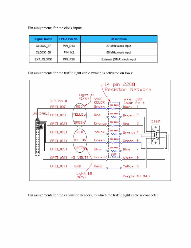
Pin assignments for the traffic light cable (which is activated on low):
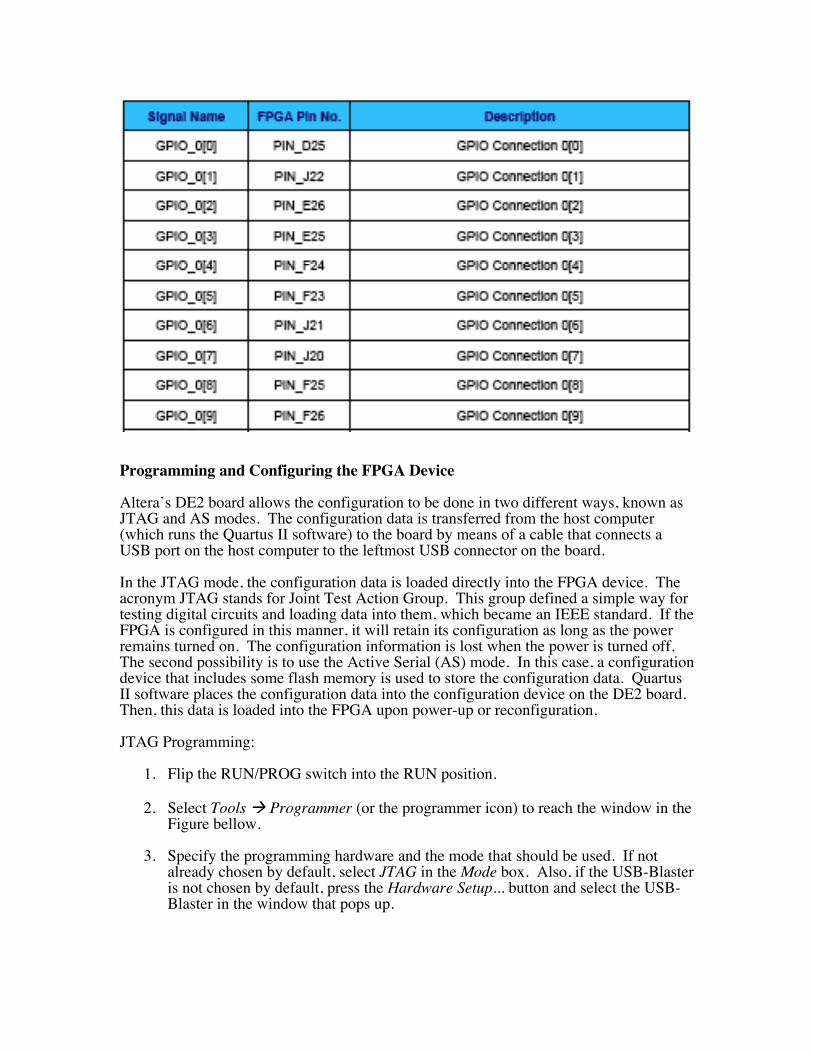
Pin assignments for the expansion headers, to which the traffic light cable is connected:
Programming and Configuring the FPGA Device Altera’s DE2 board allows the configuration to be done in two different ways, known as JTAG and AS modes. The configuration data is transferred from the host computer (which runs the Quartus II software) to the board by means of a cable that connects a USB port on the host computer to the leftmost USB connector on the board. In the JTAG mode, the configuration data is loaded directly into the FPGA device. The acronym JTAG stands for Joint Test Action Group. This group defined a simple way for testing digital circuits and loading data into them, which became an IEEE standard. If the FPGA is configured in this manner, it will retain its configuration as long as the power remains turned on. The configuration information is lost when the power is turned off. The second possibility is to use the Active Serial (AS) mode. In this case, a configuration device that includes some flash memory is used to store the configuration data. Quartus II software places the configuration data into the configuration device on the DE2 board. Then, this data is loaded into the FPGA upon power-up or reconfiguration. JTAG Programming:
1. Flip the RUN/PROG switch into the RUN position.
2. Select Tools Programmer (or the programmer icon) to reach the window in the Figure bellow.
3. Specify the programming hardware and the mode that should be used. If not already chosen by default, select JTAG in the Mode box. Also, if the USB-Blaster is not chosen by default, press the Hardware Setup... button and select the USB-Blaster in the window that pops up.

4. Observe that the configuration file <project name>.sof is listed in the window. If the file is not already listed then click Add File… and select it. This is a binary file produced by the Compiler’s Assembler module, which contains the data needed to configure the FPGA device. The extension .sof stands for SRAM Object File. Note also that the device selected is EP2C35F672, which is the FPGA device used on the DE2 board. Click on the Program/Configure check box, as shown in the Figure above.
5. Press Start in the window above. The Progress box will indicate when the configuration and programming process is completed.
Active Serial Mode Programming: (Useful to keep the program when FPGA is disconnected from the power supply)
1. In this case, the configuration data has to be loaded into the configuration device on the DE2 board, which is identified by the name EPCS16. To specify the required configuration device select Assignments Device, click on the Device & Pin Options button, and click on the Configuration tab. In the Configuration device box (which may be set to Auto) choose EPCS16 and click OK. Click OK.
2. Recompile your design.
3. Flip the RUN/PROG switch into the PROG position.
4. Select Tools Programmer. In the Mode box select Active Serial Programming. If you are changing the mode from the previously used JTAG mode, a pop-up box will appear, asking if you want to clear all devices. Click Yes. Make sure that the Hardware Setup indicates the USB-Blaster. If the configuration file is not already listed in the window, press Add File. Select the file <project name>.pof in your project directory and click Open. This is a binary file produced by the Compiler’s Assembler module, which contains the data to be loaded into the EPCS16 configuration device. The extension .pof stands for Programmer Object File. Upon returning to the Programmer window, click on the Program/Configure check box.
5. Press Start. The Progress box will indicate when the configuration and programming process is completed.
6. You may now disconnect the board, move it, then reconnect it to the power

supply.
7. Flip the RUN/PROG switch back into the RUN position and reset the board by pressing the red button.


![Abbreviated New Drug Application [ANDA]](https://img.pdfslide.us/doc/110x75/589d02af1a28ab255c8b534b/abbreviated-new-drug-application-anda.jpg)