Embed Size (px)
Citation preview

Getting Started with Altera Quartus II
NOTE: Step 1 and Step 2 are to be followed only if you are installing Altera Quartus II for the first
time. If you are using EECS commons or lab computers, you can start with Step 3 as the software is
pre-installed.
Step 1: Install the Altera Quartus 7.1 CD that comes with your book
1.) The Quartus II CAD software can be installed by running the following command in the command
prompt: Start->Programs->Accesories->Command
<CD-ROM drive>:\CDROM\Quartus_II\72sp2_quartus_free.exe
(For my computer the CD-ROM drive was H:)
2.) The installation process involves a series of steps.Choosing a complete install will require
approximately 1.5 GB of free space.Make sure you have enough space on your target directory.
Step 2: Obtaining the license file
1.) After the installation you need a license file which has to be downloaded.
2.) Open your browser and go to www.altera.com/licensing
3.) Click on the Get licenses link which is the first blue link on the page
4.) Click on Get a license for Quartus® II Web Edition software and the ModelSim®-Altera Web
Edition software that is also the first link on the page
5.) You should create an account using your e-mail address. Alternatively, you can use the Get one
time access option. You will be asked to enter information about you in this process.
6.) Once you have an username and password you can go back to Step 2.5 and now enter the username
and password.
7.) As part of the procedure you will be asked to provide your network interface card number.
The Network Interface Card (NIC) number is a 12-digit hexadecimal number that identifies your
computer. You can find the NIC number for your network card by typing at a
command prompt. Your NIC number is the number on the physical address line, minus the dashes, for
example,
So, to obtain this number, type the following command in a Windows Command Prompt window:

Look for the line of the form
The last part of this line is the network interface card number. In this example, you would type
(without the - dashes) into the box that says "Enter your network interface card
(NIC) number:" on the licensing web page.
Once you have provided to Altera the required information to obtain your license file, the file will be
emailed to you along with instructions on using the license file. The email is normally returned to you
from Altera in less than one hour.
(Reference: README file of the Altera Quartus 7.1 CD)
8.) The instructions to download and specify the license file to Altera will be given to you in your e-
mail which has the license file
Step:3 Creating a New Project
Let us design, compile and simulate a simple three input AND gate:
1.) After obtaining the license you can start working on Quartus by creating a project. Go to File-
>Create New Project wizard
2.) In the window that pops up you have to enter the directory where you want to store your project
files, the file name and a project name and click Next. (Note: The file name should be the same as
your top-level entity). This is shown in Fig. 1
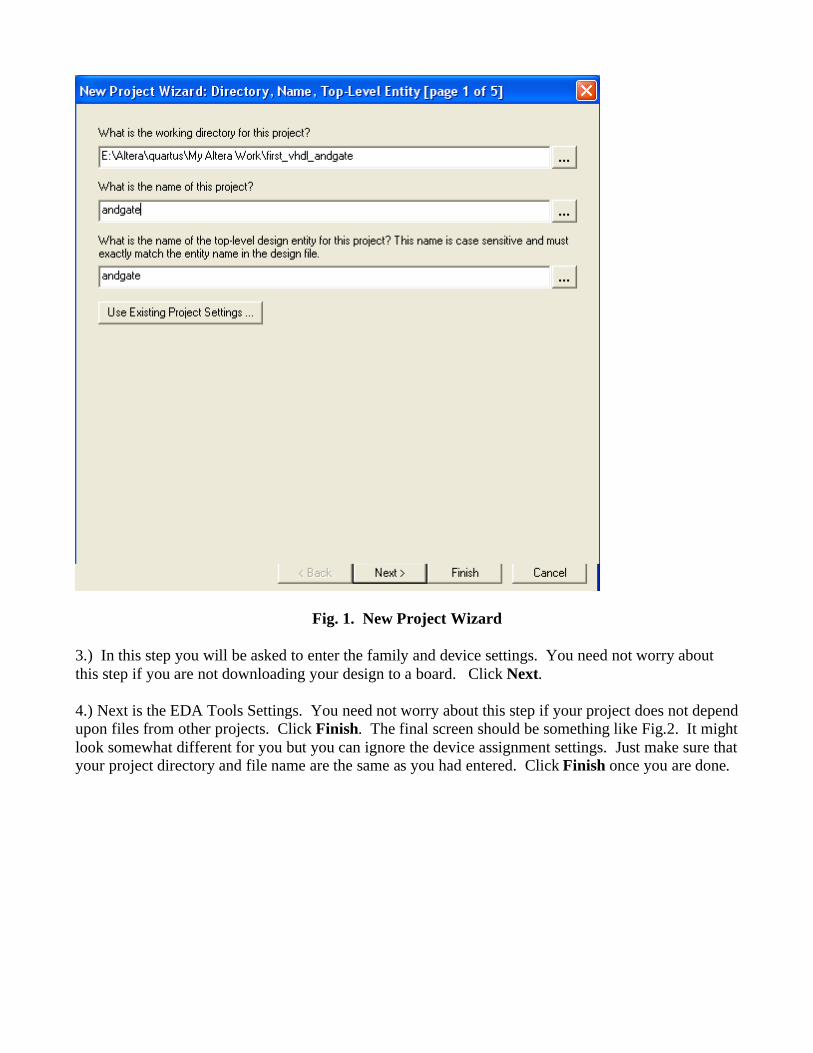
Fig. 1. New Project Wizard
3.) In this step you will be asked to enter the family and device settings. You need not worry about
this step if you are not downloading your design to a board. Click Next.
4.) Next is the EDA Tools Settings. You need not worry about this step if your project does not depend
upon files from other projects. Click Finish. The final screen should be something like Fig.2. It might
look somewhat different for you but you can ignore the device assignment settings. Just make sure that
your project directory and file name are the same as you had entered. Click Finish once you are done.
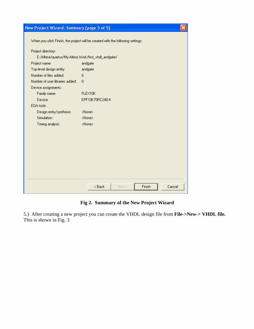
Fig 2. Summary of the New Project Wizard
5.) After creating a new project you can create the VHDL design file from File->New-> VHDL file.
This is shown in Fig. 3
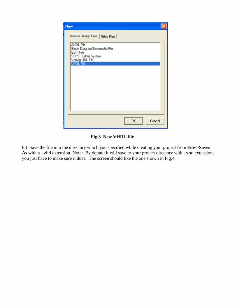
Fig.3 New VHDL file
6.) Save the file into the directory which you specified while creating your project from File->Saves
As with a extension Note: By default it will save to your project directory with extension;
you just have to make sure it does. The screen should like the one shown in Fig.4.
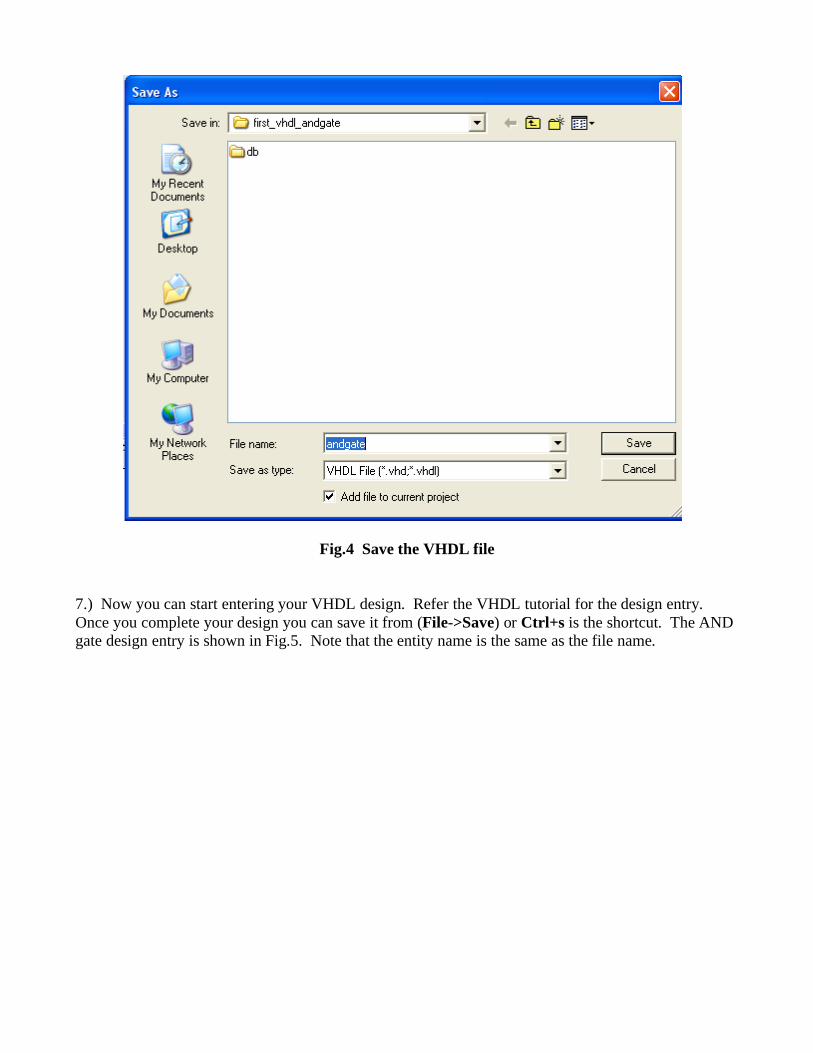
Fig.4 Save the VHDL file
7.) Now you can start entering your VHDL design. Refer the VHDL tutorial for the design entry.
Once you complete your design you can save it from (File->Save) or Ctrl+s is the shortcut. The AND
gate design entry is shown in Fig.5. Note that the entity name is the same as the file name.
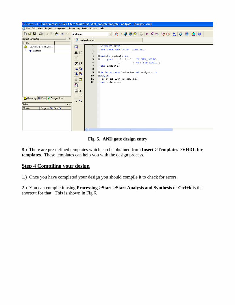
Fig. 5. AND gate design entry
8.) There are pre-defined templates which can be obtained from Insert->Templates->VHDL for
templates. These templates can help you with the design process.
Step 4 Compiling your design
1.) Once you have completed your design you should compile it to check for errors.
2.) You can compile it using Processing->Start->Start Analysis and Synthesis or Ctrl+k is the
shortcut for that. This is shown in Fig 6.
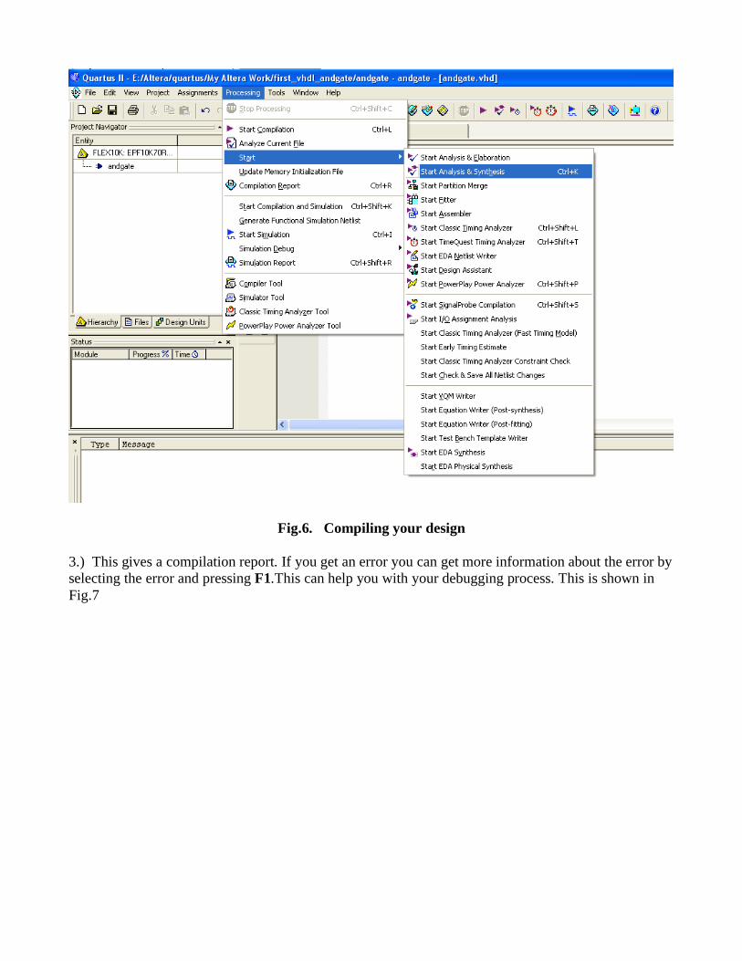
Fig.6. Compiling your design
3.) This gives a compilation report. If you get an error you can get more information about the error by
selecting the error and pressing F1.This can help you with your debugging process. This is shown in
Fig.7
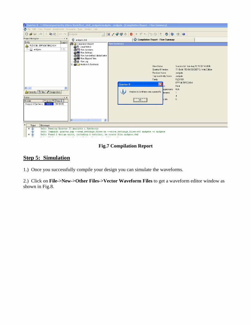
Fig.7 Compilation Report
Step 5: Simulation
1.) Once you successfully compile your design you can simulate the waveforms.
2.) Click on File->New->Other Files->Vector Waveform Files to get a waveform editor window as
shown in Fig.8.
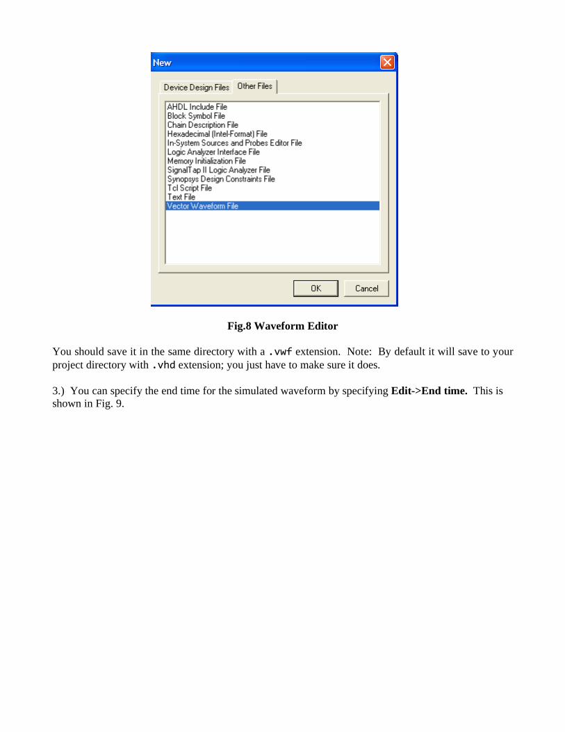
Fig.8 Waveform Editor
You should save it in the same directory with a extension. Note: By default it will save to your
project directory with extension; you just have to make sure it does.
3.) You can specify the end time for the simulated waveform by specifying Edit->End time. This is
shown in Fig. 9.
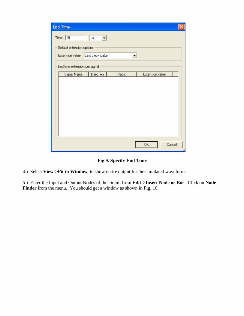
Fig 9. Specify End Time
4.) Select View->Fit in Window, to show entire output for the simulated waveform.
5.) Enter the Input and Output Nodes of the circuit from Edit->Insert Node or Bus. Click on Node
Finder from the menu. You should get a window as shown in Fig. 10.
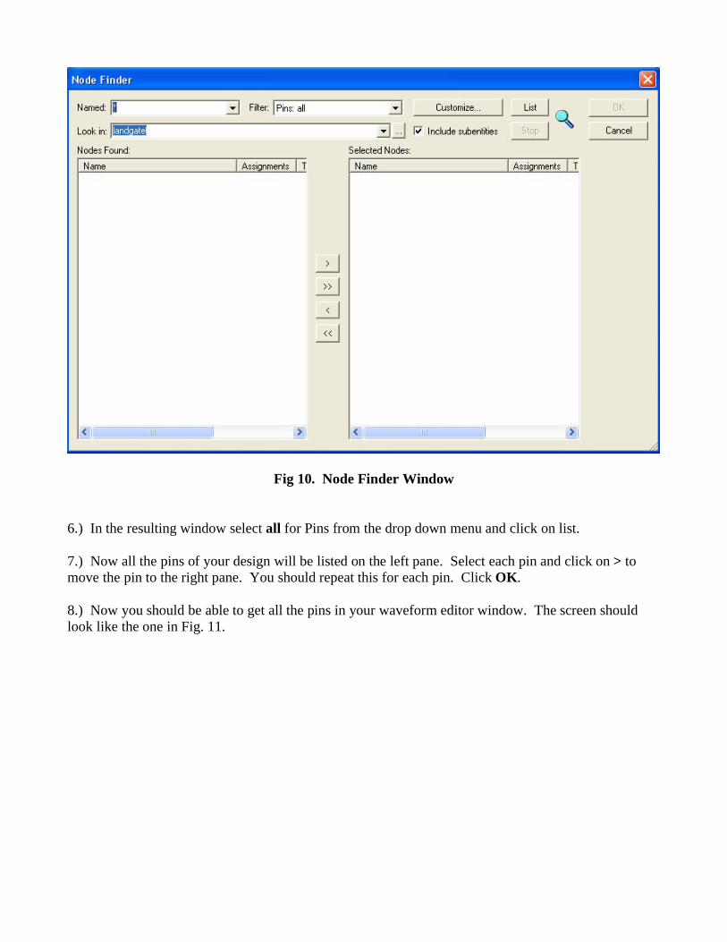
Fig 10. Node Finder Window
6.) In the resulting window select all for Pins from the drop down menu and click on list.
7.) Now all the pins of your design will be listed on the left pane. Select each pin and click on > to
move the pin to the right pane. You should repeat this for each pin. Click OK.
8.) Now you should be able to get all the pins in your waveform editor window. The screen should
look like the one in Fig. 11.
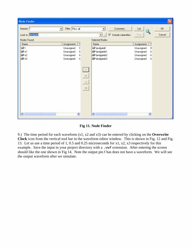
Fig 11. Node Finder
9.) The time period for each waveform (x1, x2 and x3) can be entered by clicking on the Overwrite
Clock icon from the vertical tool bar in the waveform editor window. This is shown in Fig. 12 and Fig.
13. Let us use a time period of 1, 0.5 and 0.25 microseconds for x1, x2, x3 respectively for this
example. Save the input in your project directory with a extension. After entering the screen
should like the one shown in Fig 14. Note the output pin f has does not have a waveform. We will see
the output waveform after we simulate.
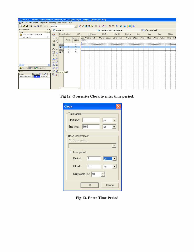
Fig 12. Overwrite Clock to enter time period.
Fig 13. Enter Time Period
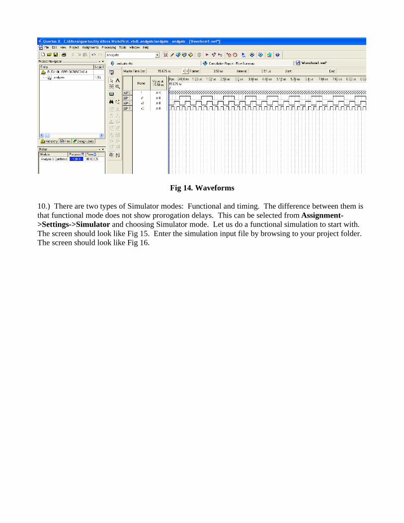
Fig 14. Waveforms
10.) There are two types of Simulator modes: Functional and timing. The difference between them is
that functional mode does not show prorogation delays. This can be selected from Assignment-
>Settings->Simulator and choosing Simulator mode. Let us do a functional simulation to start with.
The screen should look like Fig 15. Enter the simulation input file by browsing to your project folder.
The screen should look like Fig 16.
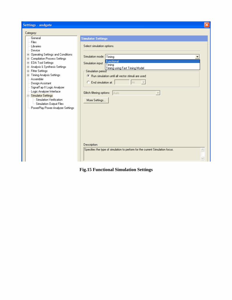
Fig.15 Functional Simulation Settings
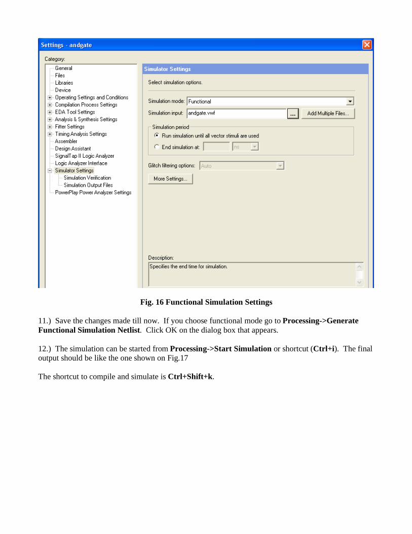
Fig. 16 Functional Simulation Settings
11.) Save the changes made till now. If you choose functional mode go to Processing->Generate
Functional Simulation Netlist. Click OK on the dialog box that appears.
12.) The simulation can be started from Processing->Start Simulation or shortcut (Ctrl+i). The final
output should be like the one shown on Fig.17
The shortcut to compile and simulate is Ctrl+Shift+k.
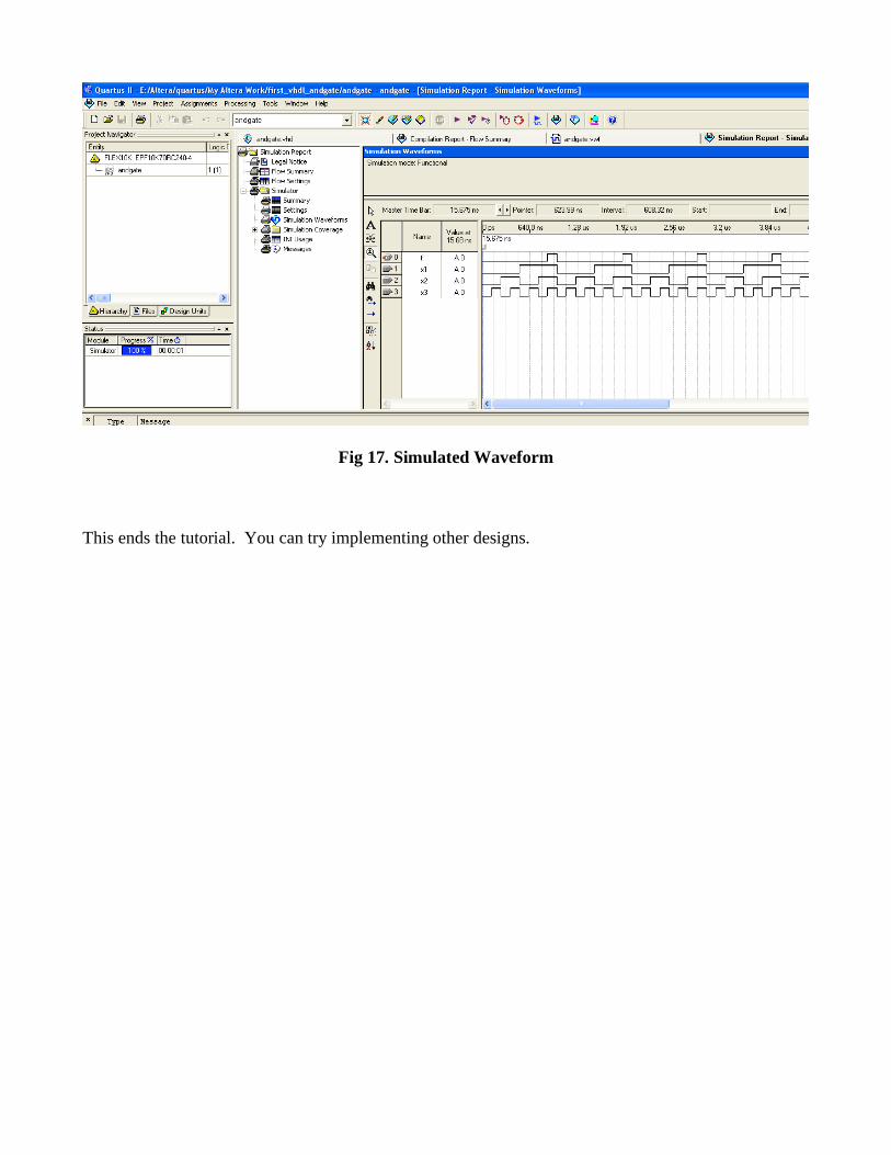
Fig 17. Simulated Waveform
This ends the tutorial. You can try implementing other designs.