Embed Size (px)
Citation preview
iQUALCOMM Incorporated, ASIC Products http://www.qualcomm.com/ProdTech/asic6455 Lusk Boulevard, San Diego, CA 92121-2779, USA E-mail: [email protected] Products Data Book, 80-24127-1 A, 8/97 Telephone: (619) 658-5005Data Subject to Change Without Notice Fax: (619) 658-1556
QUALCOMMASIC PRODUCTS
APPLICATIONSQUALCOMM ASIC Products provide complex solutions for a variety of wireless communications applications.
• Cellular
• Personal Communications Services (PCS)
• Wireless Local Loop (WLL)
• Satellite Communications
• Direct Broadcast by Satellite (DBS)
• Very Small Aperture Terminal (VSAT)
• RADAR
• Digital Radio
• Mobile Radio
• Synthesizers
• Voice Storage
• Security
• Instrumentation
ADVANTAGESFrom high performance building blocks to complete “systems-on-a-chip”, these integrated circuits and modular
devices meet the design challenges of today’s advanced communication companies.
• High Performance
• Small Size
• Cost Effective
• Reliable
• Competitive Pricing
• On-time Delivery
• Pre and Post Sales Service
PRODUCTSProduct offerings include a complete selection of integrated circuits for frequency synthesis, forward error
correction (FEC), voice compression, automatic gain control (AGC) and code division multiple access (CDMA).
Frequency synthesizer products encompass direct digital synthesizers (DDS), phase-locked loop (PLL) frequency
synthesizers and frequency synthesizer evalutaion boards implementing DDS, PLL and hybrid systems. FEC
devices include industry leading Viterbi decoders and trellis codecs. Voice compression products include variable
rate vocoders and vocoder evaluation boards. AGC amplifiers include both receive (Rx AGC) and transmit (Tx
AGC) components. CDMA ASICs include the mobile station modem (MSM), analog baseband processor (BBA),
and cell site modem (CSM).
SYNTHESIZER PRODUCTSDATA BOOK
80-24127-1 A 8/97
iiQUALCOMM Incorporated, ASIC Products http://www.qualcomm.com/ProdTech/asic6455 Lusk Boulevard, San Diego, CA 92121-2779, USA E-mail: [email protected] Products Data Book, 80-24127-1 A, 8/97 Telephone: (619) 658-5005Data Subject to Change Without Notice Fax: (619) 658-1556
INCLUDED SECTIONSDIRECT DIGITAL SYNTHESIZERS OVERVIEW (Section 1) ......................................................................... 1-1 to 1-8
Q2240 DDS (Section 2) ............................................................................................................................ 2-1 to 2-29
Q2368 Dual DDS (Section 3) .................................................................................................................. 3-1 to 3-43
Q2334 Dual DDS (Section 4) .................................................................................................................. 4-1 to 4-21
Complex Waveform Using Direct Digital Synthesizer Techniques
- Application Note (Section 5) ......................................................................................................... 5-1 to 5-3
Q2240 High Speed General Purpose DDS
- Article Reprint (Section 6) ............................................................................................................. 6-1 to 6-5
Q2368 High Speed Dual DDS for Globalstar
- Article Reprint (Section 7) ............................................................................................................. 7-1 to 7-8
Q3236 PHASE-LOCKED LOOP FREQUENCY SYNTHESIZER (Section 8) ................................................ 8-1 to 8-43
Hybrid PLL/DDS Frequency Synthesizers
- Application Note (Section 9) ....................................................................................................... 9-1 to 9-10
ORDERING INFORMATION ....................................................................................................................................... iii
RELATED QUALCOMM LITERATURE...................................................................................................................... iii
1-1QUALCOMM Incorporated, ASIC Products http://www.qualcomm.com/ProdTech/asic6455 Lusk Boulevard, San Diego, CA 92121-2779, USA E-mail: [email protected] Products Data Book, 80-24127-1 A, 8/97 Telephone: (619) 658-5005Data Subject to Change Without Notice Fax: (619) 658-1556
DIRECT DIGITALSYNTHESIZERSOVERVIEW
DIRECT DIGITAL SYNTHESIZERS IN PRACTICEDirect Digital Synthesis (DDS) can be practically
defined as a means of generating highly accurate and
harmonically pure digital representations of signals.
This digital representation is then reconstructed with
a high-speed Digital-to-Analog (DAC) Converter to
provide an analog output signal, typically a sinusoidal
tone or sequence of tones. Many high performance
DACs with greater clock speed and resolution
capability are now available to obtain extremely low
spurious from the DDS-DAC output. Since the DDS
device output is digitally processed, the DDS
functionality is easily software-configurable, making
built-in utility more flexible.
DDS techniques offer unique capabilities in
contrast to other synthesis methods. Although
limited by the Nyquist criteria (up to 1⁄2 the frequency
of the applied clock reference), DDS allows frequency
resolution control on the order of milli-hertz step size
and can likewise allow milli-hertz or even nano-hertz
of phase resolution control. Additionally, DDS
imposes no settling time constraint for frequency
changes other than what is required for digital control.
This results in extremely fast frequency switching
speeds, on the order of nanoseconds or a few
microseconds. All frequency changes are
automatically completed in a phase continuous
fashion; that is, a change to a new frequency
continues in-phase from the last point in the previous
frequency. Since the signal being generated is in the
digital domain, it can be manipulated with
exceptional accuracy. This allows precise control of
frequency or phase and can readily accommodate
frequency and phase modulation, i.e. FSK or PSK. If
desired, a microprocessor-controlled system can be
utilized to store open loop compensation data vs.
frequency for a particular device or system parameter.
The microprocessor can then simply control the DDS
to dynamically correct the frequency as needed. With
a suitable frequency detector in a receive system, a
closed loop system can easily be constructed.
1-2QUALCOMM Incorporated, ASIC Products http://www.qualcomm.com/ProdTech/asic6455 Lusk Boulevard, San Diego, CA 92121-2779, USA E-mail: [email protected] Products Data Book, 80-24127-1 A, 8/97 Telephone: (619) 658-5005Data Subject to Change Without Notice Fax: (619) 658-1556
CONTENTSDIRECT DIGITAL SYNTHESIZERS IN PRACTICE .................................................................................................. 1-1
THEORY OF OPERATION .......................................................................................................................................... 1-3
General DDS Operation ....................................................................................................................................... 1-3
Phase Increment Value ......................................................................................................................................... 1-3
Frequency Resolution ........................................................................................................................................... 1-4
Typical DDS Application ..................................................................................................................................... 1-4
Spectral Purity ...................................................................................................................................................... 1-4
Clock Source ................................................................................................................................................ 1-5
Phase Truncation......................................................................................................................................... 1-5
Amplitude Quantization ............................................................................................................................. 1-5
Spurs Due To Sampling And DAC Non-Linearities .................................................................................. 1-5
AVOIDING ALIASED IMAGES ................................................................................................................................... 1-5
USING THE MSB OUTPUT AS A PROGRAMMABLE CLOCK SOURCE .............................................................. 1-6
DDS CIRCUIT DESIGN CONSIDERATIONS............................................................................................................ 1-6
RECOMMENDED DACS ............................................................................................................................................. 1-6
DIVIDED/MULTIPLIED/TRANSLATED DDS FUNDAMENTAL OR IMAGE ....................................................... 1-7
LINEAR PHASE SHIFTING USING OFFSET FREQUENCY TECHNIQUES........................................................... 1-8
Application Example ............................................................................................................................................ 1-8
1-3QUALCOMM Incorporated, ASIC Products http://www.qualcomm.com/ProdTech/asic6455 Lusk Boulevard, San Diego, CA 92121-2779, USA E-mail: [email protected] Products Data Book, 80-24127-1 A, 8/97 Telephone: (619) 658-5005Data Subject to Change Without Notice Fax: (619) 658-1556
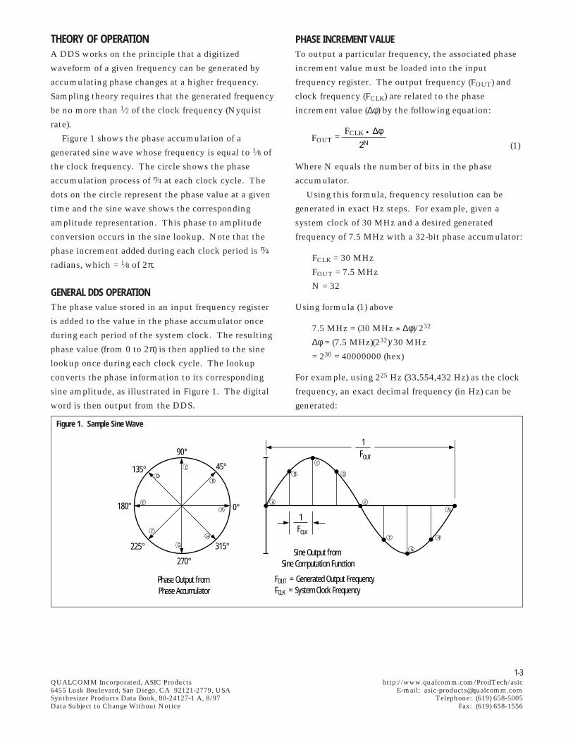
THEORY OF OPERATIONA DDS works on the principle that a digitized
waveform of a given frequency can be generated by
accumulating phase changes at a higher frequency.
Sampling theory requires that the generated frequency
be no more than 1⁄2 of the clock frequency (Nyquist
rate).
Figure 1 shows the phase accumulation of a
generated sine wave whose frequency is equal to 1⁄8 of
the clock frequency. The circle shows the phase
accumulation process of π⁄4 at each clock cycle. The
dots on the circle represent the phase value at a given
time and the sine wave shows the corresponding
amplitude representation. This phase to amplitude
conversion occurs in the sine lookup. Note that the
phase increment added during each clock period is π⁄4
radians, which = 1⁄8 of 2π.
GENERAL DDS OPERATIONThe phase value stored in an input frequency register
is added to the value in the phase accumulator once
during each period of the system clock. The resulting
phase value (from 0 to 2π) is then applied to the sine
lookup once during each clock cycle. The lookup
converts the phase information to its corresponding
sine amplitude, as illustrated in Figure 1. The digital
word is then output from the DDS.
PHASE INCREMENT VALUETo output a particular frequency, the associated phase
increment value must be loaded into the input
frequency register. The output frequency (FOUT) and
clock frequency (FCLK) are related to the phase
increment value (∆φ) by the following equation:
(1)
Where N equals the number of bits in the phase
accumulator.
Using this formula, frequency resolution can be
generated in exact Hz steps. For example, given a
system clock of 30 MHz and a desired generated
frequency of 7.5 MHz with a 32-bit phase accumulator:
FCLK = 30 MHz
FOUT = 7.5 MHz
N = 32
Using formula (1) above
7.5 MHz = (30 MHz * ∆φ)/232
∆φ = (7.5 MHz)(232)/30 MHz
= 230 = 40000000 (hex)
For example, using 225 Hz (33,554,432 Hz) as the clock
frequency, an exact decimal frequency (in Hz) can be
generated:
FCLK • ∆φ2ΝFOUT =
Figure 1. Sample Sine Wave
0°180°
45°135°
90°
225° 315°
270°
F 1
OUT
F 1
CLK
FOUT = Generated Output FrequencyFCLK = System Clock Frequency
Phase Output from Phase Accumulator
Sine Output from Sine Computation Function
A
B
C
D
E
F
G
H
A
B
C
D
E
F
G
H
A
1-4QUALCOMM Incorporated, ASIC Products http://www.qualcomm.com/ProdTech/asic6455 Lusk Boulevard, San Diego, CA 92121-2779, USA E-mail: [email protected] Products Data Book, 80-24127-1 A, 8/97 Telephone: (619) 658-5005Data Subject to Change Without Notice Fax: (619) 658-1556
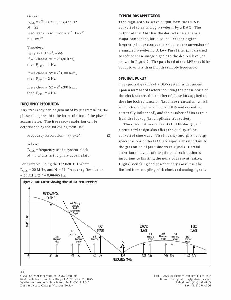
Given:
FCLK = 225 Hz = 33,554,432 Hz
N = 32
Frequency Resolution = 225 Hz/232
= 1 Hz/27
Therefore:
FOUT = (1 Hz/27) * ∆φIf we choose ∆φ = 27 (80 hex),
then FOUT = 1 Hz
If we choose ∆φ = 28 (100 hex),
then FOUT = 2 Hz
If we choose ∆φ = 29 (200 hex),
then FOUT = 4 Hz
FREQUENCY RESOLUTIONAny frequency can be generated by programming the
phase change within the bit resolution of the phase
accumulator. The frequency resolution can be
determined by the following formula:
Frequency Resolution = FCLK/2N (2)
Where:
FCLK = frequency of the system clock
N = # of bits in the phase accumulator
For example, using the Q2368I-1S1 where
FCLK = 20 MHz, and N = 32, Frequency Resolution
= 20 MHz/232 = 0.00465 Hz.
TYPICAL DDS APPLICATIONEach digitized sine wave output from the DDS is
converted to an analog waveform by a DAC. The
output of the DAC has the desired sine wave as a
major component, but also includes the higher
frequency image components due to the conversion of
a sampled waveform. A Low Pass Filter (LPF) is used
to reduce these image signals to the desired level, as
shown in Figure 2. The pass band of the LPF should be
equal to or less than half the sample frequency.
SPECTRAL PURITYThe spectral quality of a DDS system is dependent
upon a number of factors including the phase noise of
the clock source, the number of phase bits applied to
the sine lookup function (i.e. phase truncation, which
is an internal operation of the DDS and cannot be
externally influenced), and the number of bits output
from the lookup (i.e. amplitude truncation).
The specifications of the DAC, LPF design, and
circuit card design also affect the quality of the
converted sine wave. The linearity and glitch energy
specifications of the DAC are especially important to
the generation of pure sine wave signals. Careful
attention to layout of the printed circuit design is
important to limiting the noise of the synthesizer.
Digital switching and power supply noise must be
limited from coupling with clock and analog signals.
Figure 2. DDS Output Showing Effect of DAC Non-Linearities
AMPL
ITUDE
0 24 28 48 52 72 76 100FREQUENCY (MHz)
124 128 148 152 172 176
FIRSTIMAGE
SECONDIMAGE
THIRDIMAGE
FS
3rdHarmonic
Alias
2ndHarmonic
Image
2ndHarmonic
3rdHarmonic
3rdHarmonic
Image
2ndHarmonic
Image
2ndHarmonic
Image
3rdHarmonic
Image
Anti-AliasingLow PassFilter for
FundamentalOutput
FUNDAMENTALOUTPUT
1-5QUALCOMM Incorporated, ASIC Products http://www.qualcomm.com/ProdTech/asic6455 Lusk Boulevard, San Diego, CA 92121-2779, USA E-mail: [email protected] Products Data Book, 80-24127-1 A, 8/97 Telephone: (619) 658-5005Data Subject to Change Without Notice Fax: (619) 658-1556
CLOCK SOURCEThe clock source input to a DDS system is the major
contributor to the phase noise of the system, even
though its effect is reduced by the frequency division
process of the DDS. The phase noise of the DDS
output will show an improvement over phase noise of
the clock source itself of 20* log(FCLK/FOUT), where
FCLK is the system clock frequency and FOUT is the
generated frequency.
The frequency accuracy of the clock is propagated
through the DDS. Therefore, if the sampling
frequency is 100 PPM higher than desired, the output
frequency will also be higher by 100 PPM.
PHASE TRUNCATIONGiven that a DDS accumulates 32 bits of phase
information, only a portion of the Most Significant
Bits (MSB) are input to the sine lookup algorithm.
This reduced number of phase bits input to the sine
lookup function is called phase truncation. Phase
truncation is an internal operation of DDSs and cannot
be externally influenced. The truncation of the Least
Significant Bits (LSB) is a loss of phase information and
contributes errors. However, the spurs caused by
phase truncation errors are below 76 dBc for
QUALCOMM's DDSs.
AMPLITUDE QUANTIZATIONAmplitude quantization occurs in the sine lookup
process. The lookup takes in a fixed number of bits of
phase information and converts it to the equivalent
sine amplitude. Since an ideal sine representation
would require an infinite number of bits for most
values, the value must be truncated. QUALCOMM's
DDSs quantize the values and output the 12 MSBs as
the sine amplitude representation which is a typical
value for practical high-speed DACs.
SPURS DUE TO SAMPLING AND DAC NON-LINEARITIESThe frequencies of the discrete spurs and the
amplitude of each are dependent on the ratio of the
generated frequency (FOUT) to the clock frequency
(FCLK), as well as the phase relationship of the output
waveform to the sample clock. The 12-bit digitized
sine output theoretically will provide a broadband
signal-to-spurious ratio of 72 dB, again depending on
the quality of the DAC and the LPF design as well as
the printed circuit characteristics and the phase noise
of the clock frequency.
The DDS is able to generate frequencies from 0 Hz
to 1⁄2 the frequency of the clock. However, limitations
on the slope of the roll off of the LPF determine the
practical upper limit of the output frequency to about
40% of the clock frequency. Let FCLK indicate the
frequency of the system clock, and FOUT indicate the
generated frequency. Discrete aliased images due to
sample rate aliasing will be produced at frequencies of
FCLK - FOUT, FCLK + FOUT, 2FCLK - FOUT, 2FCLK + FOUT,
and so forth, unless the LPF filters these images to
acceptable levels (see Figure 2).
Notice a sinc [(π * FOUT ) /FCLK] envelope is
impressed upon all of the DDS outputs in Figure 2
(≈∆ 4 dB from DC up to FCLK/2).
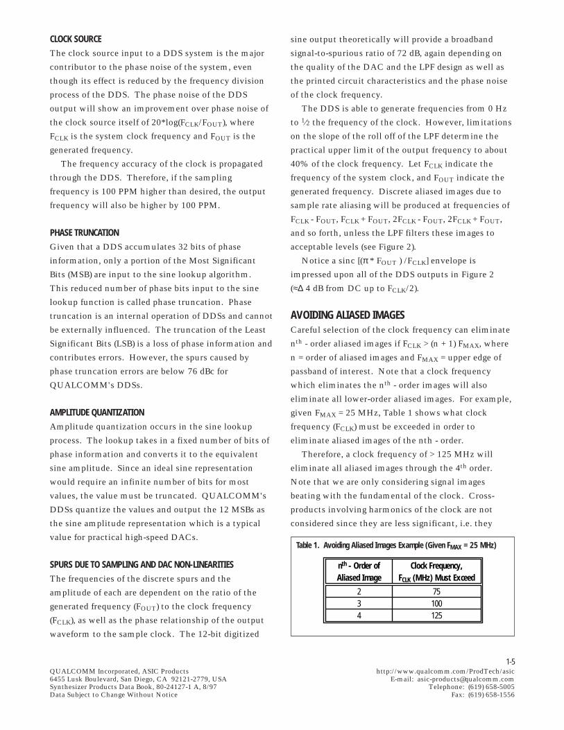
AVOIDING ALIASED IMAGESCareful selection of the clock frequency can eliminate
nth - order aliased images if FCLK > (n + 1) FMAX, where
n = order of aliased images and FMAX = upper edge of
passband of interest. Note that a clock frequency
which eliminates the nth - order images will also
eliminate all lower-order aliased images. For example,
given FMAX = 25 MHz, Table 1 shows what clock
frequency (FCLK) must be exceeded in order to
eliminate aliased images of the nth - order.
Therefore, a clock frequency of > 125 MHz will
eliminate all aliased images through the 4th order.
Note that we are only considering signal images
beating with the fundamental of the clock. Cross-
products involving harmonics of the clock are not
considered since they are less significant, i.e. they
nth - Order ofAliased Image
234
Clock Frequency,FCLK (MHz) Must Exceed
75100125
Table 1. Avoiding Aliased Images Example (Given FMAX = 25 MHz)
1-6QUALCOMM Incorporated, ASIC Products http://www.qualcomm.com/ProdTech/asic6455 Lusk Boulevard, San Diego, CA 92121-2779, USA E-mail: [email protected] Products Data Book, 80-24127-1 A, 8/97 Telephone: (619) 658-5005Data Subject to Change Without Notice Fax: (619) 658-1556
involve higher-order signal images, as well as higher-
order clock harmonics.
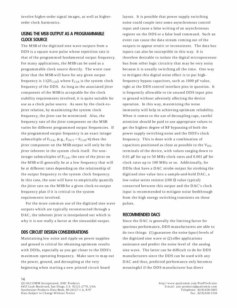
USING THE MSB OUTPUT AS A PROGRAMMABLECLOCK SOURCEThe MSB of the digitized sine wave outputs from a
DDS is a square wave pulse whose repetition rate is
that of the programmed fundamental output frequency.
For many applications, the MSB can be used as a
programmable clock source directly. The worst case
jitter that the MSB will have for any given output
frequency is 1/(2FCLK), where FCLK is the system clock
frequency of the DDS. As long as the associated jitter
component of the MSB is acceptable for the clock
stability requirements involved, it is quite suitable for
use as a clock pulse source. As seen by the clock-to-
jitter relation, by maximizing the system clock
frequency, the jitter can be minimized. Also, the
frequency rate of the jitter component on the MSB
varies for different programmed output frequencies. If
the programmed output frequency is an exact integer
submultiple of FCLK, (e.g., FOUT = FCLK/4) then the
jitter component on the MSB output will only be the
jitter inherent in the system clock itself. For non-
integer submultiples of FCLK, the rate of the jitter on
the MSB will generally be at a low frequency that will
be at different rates depending on the relationship of
the output frequency to the system clock frequency.
In this case, the user will have to empirically quantify
the jitter rate on the MSB for a given clock-to-output
frequency plan if it is critical to the system
requirements involved.
For the more common use of the digitized sine wave
outputs which are typically reconstructed through a
DAC, the inherent jitter is interpolated out which is
why it is not really a factor at the sinusoidal output.
DDS CIRCUIT DESIGN CONSIDERATIONSMaintaining low noise and ripple on power supplies
and ground is critical for obtaining optimum results
with DDSs, especially as you get closer to the DDS's
maximum operating frequency. Make sure to map out
the power, ground, and decoupling at the very
beginning when starting a new printed circuit board
layout. It is possible that power supply switching
noise could couple into some asynchronous control
input and cause a false writing of an asynchronous
register on the DDS or a false load command. Such an
event can cause the data stream coming out of the
outputs to appear erratic or inconsistent. The data bus
inputs can also be susceptible in this way. It is
therefore desirable to isolate the digital microprocessor
bus from other logic circuitry that may be very noisy
because it is usually switching all the time. One way
to mitigate this digital noise effect is to put high-
frequency bypass capacitors, such as 1000 pF value,
right at the DDS control interface pins in question. It
is frequently allowable to tie unused DDS input pins
to ground without adversely affecting the device
operation. In this way, maximizing the noise
immunity will help in achieving optimum reliability.
When it comes to the use of decoupling caps, careful
attention should be paid to use appropriate values to
get the highest degree of RF bypassing of both the
power supply switching noise and the DDS's clock
frequency. This is done with a combination of
capacitors positioned as close as possible to the VDD
terminals of the device, with values ranging down to
0.01 µF for up to 50 MHz clock rates and 0.001 µF for
clock rates up to 100 MHz or so. Additionally, for
DDSs that have a DAC strobe output for strobing the
digitized sine value into a sample-and-hold DAC, a
low-value series resistor (100 Ω value typical)
connected between this output and the DAC's clock
input is recommended to mitigate noise feedthrough
from the high energy switching transients on these
pulses.
RECOMMENDED DACSSince the DAC is generally the limiting factor for
spurious performance, DDS manufacturers are able to
do two things: (1) guarantee the noise (spur) levels of
the digitized sine wave or (2) offer applications
assistance and predict the noise level of the analog
sine wave. The latter can be difficult to do for DDS
manufacturers since the DDS can be used with any
DAC and thus, predicted performance only becomes
meaningful if the DDS manufacturer has direct
1-7QUALCOMM Incorporated, ASIC Products http://www.qualcomm.com/ProdTech/asic6455 Lusk Boulevard, San Diego, CA 92121-2779, USA E-mail: [email protected] Products Data Book, 80-24127-1 A, 8/97 Telephone: (619) 658-5005Data Subject to Change Without Notice Fax: (619) 658-1556
experience in empirically qualifying a particular type
DAC with a given DDS. After extensive testing, it is
our recommendation in applications where faster clock
rates or higher output frequencies are applied, the best
Spurious-Free-Dynamic-Range (SFDR) performance
will be achieved with DACs having ultra low
switching transients (glitch energy) and very fast
settling time, although the practical tradeoff for total
integrated noise performance generally means using a
DAC of at least 10-bits of resolution. Different DACs
may be appropriate for a specific system but it seems
the only real way to compare DACs and validate
performance is to build test circuits using them.
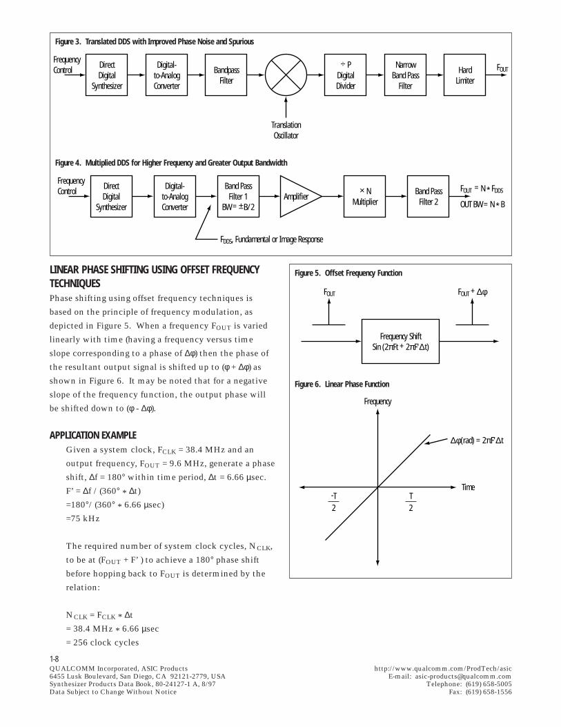
DIVIDED/MULTIPLIED/TRANSLATED DDSFUNDAMENTAL OR IMAGEOne of the limitations surrounding DDS for L.O.
generation is the fact that the fundamental frequency
that can be achieved is restricted to ≈ 40% of the clock
frequency capability. This limitation can frequently be
sidestepped by taking advantage of the image responses
that are automatically generated as a byproduct of the
sampling techniques that occur within the DDS
architecture. The images will occur at multiples of the
clock frequency ± the generated fundamental output
frequency, as shown in Figure 2. In other words,
DDS Image Responses = N * FCLK ± FOUT
where N = 1,2,3…
There are certain things to note when trying to utilize
DDS image responses. First, whether we're referring to
a fundamental output or an imaged output, the DAC's
nonlinearities or "glitches" may contribute harmonics
of the fundamental output which may fold into the
desired passband. Secondly, the Sin(x)/x amplitude
envelope impressed upon all DDS fundamental and
image outputs, will inherently create lower amplitude
image signals compared to the fundamental. This
results in a lower SFDR for the image output but can
be improved by using a DAC with excellent linearity
and perhaps D/A de-glitching techniques. It's
important to note, however, that the actual phase
noise performance at the image response will be the
same as that of the fundamental output frequency.
The kinds of applications best-suited for utilizing an
image signal involve generating a narrowband L.O. or
I.F. frequency using the first or second image response.
If there are any output tuning requirements, they
should be constrained to a very narrowband range so as
to allow for the use of a very selective bandpass filter
to attenuate all unwanted spurious outputs.
Various "tricks" can be applied to any fundamental
or image response to both maximize spectral purity,
and achieve a higher range of final output frequencies.
One such method is to upconvert the output of the
DDS/DAC and then cascade with a digital divider to
get the desired frequency, as shown in Figure 3. The
limiter will suppress any AM spurs, and the divider
can be used to divide the DDS output to provide an
appropriate center frequency for a particular filter
technology (such as a crystal filter, where the range of
center frequencies may be limited), or simply to
improve its phase noise and spurious performance
(20 LOG[P] dB improvement, ideally). Another such
method to achieve both a higher frequency and a
widened tuning bandwidth is to cascade the output of
the DDS/DAC with a multiplier and associated
filtering, as shown in Figure 4. The first bandpass
filter keeps the DDS-generated spurious tones and
noise confined to the filter bandwidth of ± B/2. After
frequency multiplication by N, the noise and spurious
tones will be degraded by 20 LOG[N] dB, but only
within ± B/2 of the output frequency. That is to say,
the output spectrum is a clean tone surrounded by a
pedestal of noise and spurs. The pedestal width is
equal to B, with noise and spurs falling off rapidly
beyond this point. The final output frequency is FOUT
= N * FDDS, and the output tuning bandwidth is N * B.
In essence, bandpass filter 1 serves as a tuneable high-
frequency tracking filter, but is actually a fixed, low-
frequency design. The amplifier provides sufficient
drive level into the passive multiplier, and bandpass
filter 2 pre-selects the desired harmonic and suppresses
other harmonic spurious. Any AM spurious
components from the DDS are no larger at the output
of a multiplier than at the input, so these can be
suppressed by a limiter before or after frequency
multiplication, if desired.
1-8QUALCOMM Incorporated, ASIC Products http://www.qualcomm.com/ProdTech/asic6455 Lusk Boulevard, San Diego, CA 92121-2779, USA E-mail: [email protected] Products Data Book, 80-24127-1 A, 8/97 Telephone: (619) 658-5005Data Subject to Change Without Notice Fax: (619) 658-1556
Figure 3. Translated DDS with Improved Phase Noise and Spurious
FrequencyControl
DirectDigital
Synthesizer
Digital-to-AnalogConverter
HardLimiter
BandpassFilter
÷ PDigitalDivider
TranslationOscillator
NarrowBand Pass
Filter
FOUT
Figure 4. Multiplied DDS for Higher Frequency and Greater Output Bandwidth
FrequencyControl
DirectDigital
Synthesizer
Digital-to-AnalogConverter
Band PassFilter 1
BW = ±B/2Amplifier
× NMultiplier
Band PassFilter 2
FOUT = N * FDDS
OUT BW = N * B
FDDS, Fundamental or Image Response
LINEAR PHASE SHIFTING USING OFFSET FREQUENCYTECHNIQUESPhase shifting using offset frequency techniques is
based on the principle of frequency modulation, as
depicted in Figure 5. When a frequency FOUT is varied
linearly with time (having a frequency versus time
slope corresponding to a phase of ∆φ) then the phase of
the resultant output signal is shifted up to (φ + ∆φ) as
shown in Figure 6. It may be noted that for a negative
slope of the frequency function, the output phase will
be shifted down to (φ - ∆φ).
Figure 5. Offset Frequency Function
Frequency ShiftSin (2πFt + 2πF'∆t)
FOUT FOUT + ∆φ
Figure 6. Linear Phase Function
∆φ(rad) = 2πF'∆t
Frequency
Time-T2
T2
APPLICATION EXAMPLEGiven a system clock, FCLK = 38.4 MHz and an
output frequency, FOUT = 9.6 MHz, generate a phase
shift, ∆f = 180° within time period, ∆t = 6.66 µsec.
F’ = ∆f / (360° * ∆t)
=180°/ (360° * 6.66 µsec)
=75 kHz
The required number of system clock cycles, NCLK,
to be at (FOUT + F’ ) to achieve a 180° phase shift
before hopping back to FOUT is determined by the
relation:
NCLK = FCLK * ∆t
= 38.4 MHz * 6.66 µsec
= 256 clock cycles
2-1QUALCOMM Incorporated, ASIC Products http://www.qualcomm.com/ProdTech/asic6455 Lusk Boulevard, San Diego, CA 92121-2779, USA E-mail: [email protected] Products Data Book, 80-24127-1 A, 8/97 Telephone: (619) 658-5005Data Subject to Change Without Notice Fax: (619) 658-1556
Q2240DIRECT DIGITALSYNTHESIZER
APPLICATIONS• Digital Radios and Modems
• PC-based Instrumentation Cards
• Handheld Test and Measurement Equipment
• Portable Communications Terminals
• Digital Signal Processors
• Specialized Mobile Radios (SMR)
• Digital Video/Audio Signal Generation
• Arbitrary Waveform or Function Generator
• Baseband Transmitters and Receivers
• Mobile/Airborne Communications
• Frequency Hopping Systems
• Local Oscillator Generation
• Cellular Base Stations
• Spread Spectrum Modulators
• HF Transceivers
• Paging Systems
FEATURES• Operation @ 5V or 3.3 V Supply
• 100 MHz Operation @ 5 V
• 60 MHz Operation @ 3.3 V
• 32-bit Input Resolution for Frequency
• 12-bit Output Resolution for Sine Wave
Amplitude
• 14-bit Output Phase Resolution for Arbitrary
Waveform Synthesis
• Q2240I-1N: Backwards Compatible with the
Q2220I-50N
• Q2240I-2S1: Serial Control Interface
• Q2240I-3S1: 32-bit Direct Parallel Control
Interface
• Q2240I-2S1: 14 x 20 mm, 64-pin PQFP
• Q2240I-3S1: 14 x 20 mm, 64-pin PQFP
• 100 MHz Frequency Update (Hop) Rate
• Arbitrary Waveform Mode
• Power-down Mode
• 3 Output Signal Formats: Offset Binary,
2’s Complement, Sign Magnitude
• Guaranteed Over Industrial Temperature and
Voltage Range
2-2QUALCOMM Incorporated, ASIC Products http://www.qualcomm.com/ProdTech/asic6455 Lusk Boulevard, San Diego, CA 92121-2779, USA E-mail: [email protected] Products Data Book, 80-24127-1 A, 8/97 Telephone: (619) 658-5005Data Subject to Change Without Notice Fax: (619) 658-1556
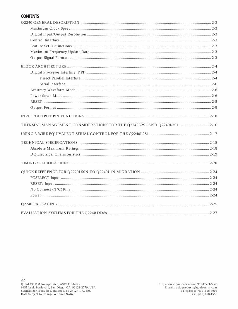
CONTENTSQ2240 GENERAL DESCRIPTION ............................................................................................................................... 2-3
Maximum Clock Speed ........................................................................................................................................ 2-3
Digital Input/Output Resolution ......................................................................................................................... 2-3
Control Interface .................................................................................................................................................. 2-3
Feature Set Distinctions ....................................................................................................................................... 2-3
Maximum Frequency Update Rate ...................................................................................................................... 2-3
Output Signal Formats ......................................................................................................................................... 2-3
BLOCK ARCHITECTURE ............................................................................................................................................ 2-4
Digital Processor Interface (DPI) .......................................................................................................................... 2-4
Direct Parallel Interface .............................................................................................................................. 2-4
Serial Interface ............................................................................................................................................. 2-6
Arbitrary Waveform Mode ................................................................................................................................... 2-6
Power-down Mode ................................................................................................................................................ 2-6
RESET ................................................................................................................................................................... 2-8
Output Format ...................................................................................................................................................... 2-8
INPUT/OUTPUT PIN FUNCTIONS......................................................................................................................... 2-10
THERMAL MANAGEMENT CONSIDERATIONS FOR THE Q2240I-2S1 AND Q2240I-3S1 ............................. 2-16
USING 3-WIRE EQUIVALENT SERIAL CONTROL FOR THE Q2240I-2S1 .......................................................... 2-17
TECHNICAL SPECIFICATIONS ............................................................................................................................... 2-18
Absolute Maximum Ratings .............................................................................................................................. 2-18
DC Electrical Characteristics ............................................................................................................................ 2-19
TIMING SPECIFICATIONS ....................................................................................................................................... 2-20
QUICK REFERENCE FOR Q2220I-50N TO Q2240I-1N MIGRATION .................................................................. 2-24
FCSELECT Input ................................................................................................................................................ 2-24
RESET/ Input ...................................................................................................................................................... 2-24
No Connect (N/C) Pins ...................................................................................................................................... 2-24
Power ................................................................................................................................................................... 2-24
Q2240 PACKAGING................................................................................................................................................... 2-25
EVALUATION SYSTEMS FOR THE Q2240 DDSs ................................................................................................... 2-27
2-3QUALCOMM Incorporated, ASIC Products http://www.qualcomm.com/ProdTech/asic6455 Lusk Boulevard, San Diego, CA 92121-2779, USA E-mail: [email protected] Products Data Book, 80-24127-1 A, 8/97 Telephone: (619) 658-5005Data Subject to Change Without Notice Fax: (619) 658-1556
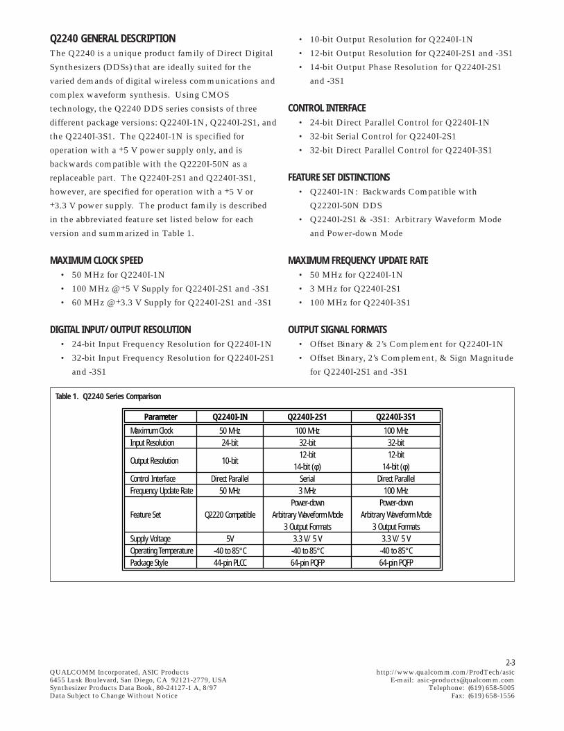
Q2240 GENERAL DESCRIPTIONThe Q2240 is a unique product family of Direct Digital
Synthesizers (DDSs) that are ideally suited for the
varied demands of digital wireless communications and
complex waveform synthesis. Using CMOS
technology, the Q2240 DDS series consists of three
different package versions: Q2240I-1N, Q2240I-2S1, and
the Q2240I-3S1. The Q2240I-1N is specified for
operation with a +5 V power supply only, and is
backwards compatible with the Q2220I-50N as a
replaceable part. The Q2240I-2S1 and Q2240I-3S1,
however, are specified for operation with a +5 V or+3.3 V power supply. The product family is described
in the abbreviated feature set listed below for each
version and summarized in Table 1.
MAXIMUM CLOCK SPEED• 50 MHz for Q2240I-1N
• 100 MHz @ +5 V Supply for Q2240I-2S1 and -3S1
• 60 MHz @ +3.3 V Supply for Q2240I-2S1 and -3S1
DIGITAL INPUT/OUTPUT RESOLUTION• 24-bit Input Frequency Resolution for Q2240I-1N
• 32-bit Input Frequency Resolution for Q2240I-2S1
and -3S1
• 10-bit Output Resolution for Q2240I-1N
• 12-bit Output Resolution for Q2240I-2S1 and -3S1
• 14-bit Output Phase Resolution for Q2240I-2S1
and -3S1
CONTROL INTERFACE• 24-bit Direct Parallel Control for Q2240I-1N
• 32-bit Serial Control for Q2240I-2S1
• 32-bit Direct Parallel Control for Q2240I-3S1
FEATURE SET DISTINCTIONS• Q2240I-1N: Backwards Compatible with
Q2220I-50N DDS
• Q2240I-2S1 & -3S1: Arbitrary Waveform Mode
and Power-down Mode
MAXIMUM FREQUENCY UPDATE RATE• 50 MHz for Q2240I-1N
• 3 MHz for Q2240I-2S1
• 100 MHz for Q2240I-3S1
OUTPUT SIGNAL FORMATS• Offset Binary & 2’s Complement for Q2240I-1N
• Offset Binary, 2’s Complement, & Sign Magnitude
for Q2240I-2S1 and -3S1
Table 1. Q2240 Series Comparison
Parameter Q2240I-IN
50 MHz24-bit
10-bit
Direct Parallel50 MHz
Q2220 Compatible
5V-40 to 85°C44-pin PLCC
Q2240I-2S1
100 MHz32-bit12-bit
14-bit (φ)Serial3 MHz
Power-downArbitrary Waveform Mode
3 Output Formats3.3 V/ 5 V
-40 to 85°C64-pin PQFP
Q2240I-3S1
100 MHz32-bit12-bit
14-bit (φ)Direct Parallel
100 MHzPower-down
Arbitrary Waveform Mode3 Output Formats
3.3 V/ 5 V-40 to 85°C64-pin PQFP
Maximum ClockInput Resolution
Output Resolution
Control InterfaceFrequency Update Rate
Feature Set
Supply VoltageOperating TemperaturePackage Style
2-4QUALCOMM Incorporated, ASIC Products http://www.qualcomm.com/ProdTech/asic6455 Lusk Boulevard, San Diego, CA 92121-2779, USA E-mail: [email protected] Products Data Book, 80-24127-1 A, 8/97 Telephone: (619) 658-5005Data Subject to Change Without Notice Fax: (619) 658-1556
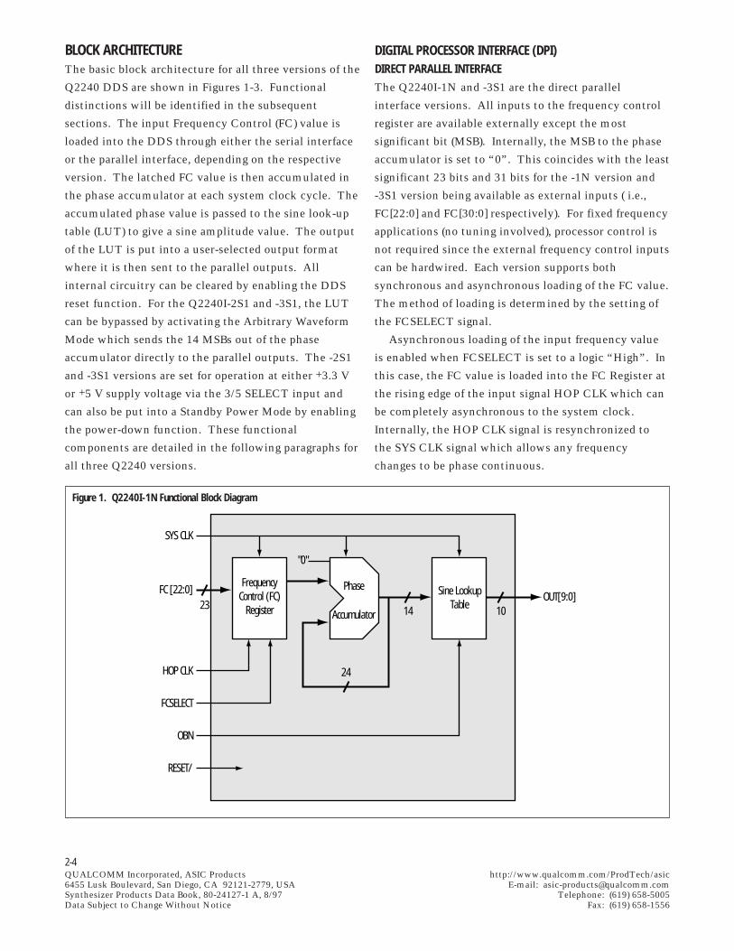
BLOCK ARCHITECTUREThe basic block architecture for all three versions of the
Q2240 DDS are shown in Figures 1-3. Functional
distinctions will be identified in the subsequent
sections. The input Frequency Control (FC) value is
loaded into the DDS through either the serial interface
or the parallel interface, depending on the respective
version. The latched FC value is then accumulated in
the phase accumulator at each system clock cycle. The
accumulated phase value is passed to the sine look-up
table (LUT) to give a sine amplitude value. The output
of the LUT is put into a user-selected output format
where it is then sent to the parallel outputs. All
internal circuitry can be cleared by enabling the DDS
reset function. For the Q2240I-2S1 and -3S1, the LUT
can be bypassed by activating the Arbitrary Waveform
Mode which sends the 14 MSBs out of the phase
accumulator directly to the parallel outputs. The -2S1
and -3S1 versions are set for operation at either +3.3 V
or +5 V supply voltage via the 3/5 SELECT input and
can also be put into a Standby Power Mode by enabling
the power-down function. These functional
components are detailed in the following paragraphs for
all three Q2240 versions.
DIGITAL PROCESSOR INTERFACE (DPI)DIRECT PARALLEL INTERFACEThe Q2240I-1N and -3S1 are the direct parallel
interface versions. All inputs to the frequency control
register are available externally except the most
significant bit (MSB). Internally, the MSB to the phase
accumulator is set to “0”. This coincides with the least
significant 23 bits and 31 bits for the -1N version and
-3S1 version being available as external inputs ( i.e.,
FC[22:0] and FC[30:0] respectively). For fixed frequency
applications (no tuning involved), processor control is
not required since the external frequency control inputs
can be hardwired. Each version supports both
synchronous and asynchronous loading of the FC value.
The method of loading is determined by the setting of
the FCSELECT signal.
Asynchronous loading of the input frequency value
is enabled when FCSELECT is set to a logic “High”. In
this case, the FC value is loaded into the FC Register at
the rising edge of the input signal HOP CLK which can
be completely asynchronous to the system clock.
Internally, the HOP CLK signal is resynchronized to
the SYS CLK signal which allows any frequency
changes to be phase continuous.
Figure 1. Q2240I-1N Functional Block Diagram
SYS CLK
FC [22:0]
HOP CLK
FCSELECT
OBN
RESET/
OUT[9:0]
"0"
Sine LookupTable
FrequencyControl (FC)
Register
Phase
Accumulator23 14
24
10
2-5QUALCOMM Incorporated, ASIC Products http://www.qualcomm.com/ProdTech/asic6455 Lusk Boulevard, San Diego, CA 92121-2779, USA E-mail: [email protected] Products Data Book, 80-24127-1 A, 8/97 Telephone: (619) 658-5005Data Subject to Change Without Notice Fax: (619) 658-1556
Figure 2. Q2240I-2S1 Functional Block Diagram
SYS CLK
SER CLKSDATA IN [30:0]
SERMODE/
HOP CLKSENABLE
SIGN MAGOBN
ARBENRESET/
PWR DN/3/5 SELECT
OUT[11:0]; [13:0]
SDATA OUT [30:0]
"0"Sine Lookup
Tableand
ARBEN Mux
Serial Buffer+
FrequencyControl (FC)
Register
Phase
Accumulator 14
32
3112;14
SYS CLK
FC[30:0]
HOP CLKFCSELECT
SIGN MAGOBN
ARBENRESET/
PWR DN/3/5 SELECT
OUT[11:0]; [13:0]
"0"Sine Lookup
Tableand
ARBEN Mux
FrequencyControl (FC)
Register
Phase
Accumulator31 14
32
3112;14
Figure 3. Q2240I-3S1 Functional Block Diagram
Alternatively, synchronous loading of the input
frequency value is enabled when FCSELECT is set to a
logic “Low”. In this case, the FC value is loaded into
the FC Register at the rising edge of each system clock
signal SYS CLK. Using synchronous loading of the
parallel inputs allows frequency changes as fast as the
system clock frequency.
The loaded FC value will be completely cleared to
zero when the input signal RESET/ is enabled. With
the Q2240I-3S1, when the Power-down Mode is enabled
the parallel interface is disabled and no new FC value
can be loaded into the FC registers.
Note that prior to loading the FC value after supply
voltage is first applied, the output of the DDS will
2-6QUALCOMM Incorporated, ASIC Products http://www.qualcomm.com/ProdTech/asic6455 Lusk Boulevard, San Diego, CA 92121-2779, USA E-mail: [email protected] Products Data Book, 80-24127-1 A, 8/97 Telephone: (619) 658-5005Data Subject to Change Without Notice Fax: (619) 658-1556
come up in a random state unless the RESET/ signal
has been pulsed “Low”. In this case, the output will be
all zeros until the FC Register is loaded.
SERIAL INTERFACESerial control of the Q2240I-2S1 is accomplished in a
standard fashion using four signals for loading in the FC
value: SDATA IN, SER CLK, SENABLE, and HOP CLK.
Note that first the input signal SERMODE/ must be
set “Low” to enable the serial interface. (SERMODE/ is
a static signal and asynchronous to any clock input.)
With the SERMODE/ input set “Low”, data is shifted
serially bit by bit into SDATA IN on the rising edge of
the SER CLK input while the shift enable control input,
SENABLE, is set “High”. To insure the timing
integrity of the serial programming bits, it is necessary
that the rising edge of the SER CLK signal does not
exceed a 10% - 90% rise time of 15 nanoseconds. The
serial programming sequence for the FC value consists
of 31 bits in the order of MSB followed by LSB. As with
the Q2240I-1N and -3S1 versions, internally the highest
MSB (bit 32) to the phase accumulator is set to “0”.
The loaded FC value is stored in the 31-bit serial buffer
registers clocked by the SER CLK signal. The
SENABLE input must be held “High” for the entire
serial programming sequence and then set “Low”.
Letting the SENABLE go “Low” before all of the serial
programming bits are loaded into the serial registers
will result in erroneous programming to the serial
registers. After the SENABLE input is set “Low”, the
serial register contents are activated on the rising edge
of the HOP CLK input according to the timing
requirements shown in Figure 13 and Table 22. A serial
data output, SDATA OUT, is provided to facilitate
daisy-chaining to another Q2240I-2S1 or other serial-
controlled devices. This means that at the same time
when the 31-bit FC value is being serially shifted into
the serial buffer registers, the last 31-bit FC value
stored in the buffer is being shifted out of the DDS
through the SDATA OUT with MSB leading LSB.
The loaded FC value will be completely cleared to
zero when the input signal RESET/ is enabled.
Additionally, when the Power-down Mode is enabled,
the serial interface which runs on SER CLK is not
disabled. This means that even during a power-down
condition, an FC value can still be serially shifted into
the serial buffer registers. In this case when the DDS is
activated to a power-up condition, the FC value can
then be loaded into the FC Register by asserting the
HOP CLK signal. Note that prior to loading the FC
value after supply voltage is first applied, the output of
the DDS will come up in a random state unless the
RESET/ signal has been pulsed “Low”. In this case, the
output will be all zeros until the FC Register is loaded.
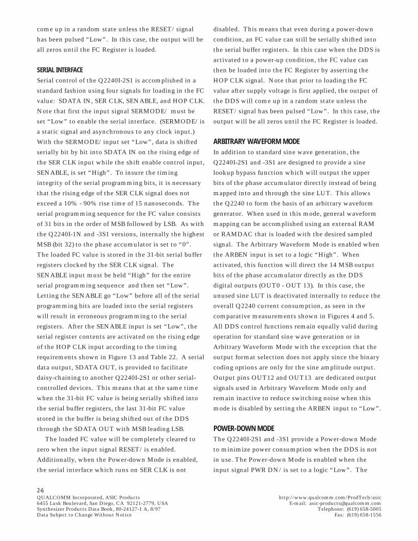
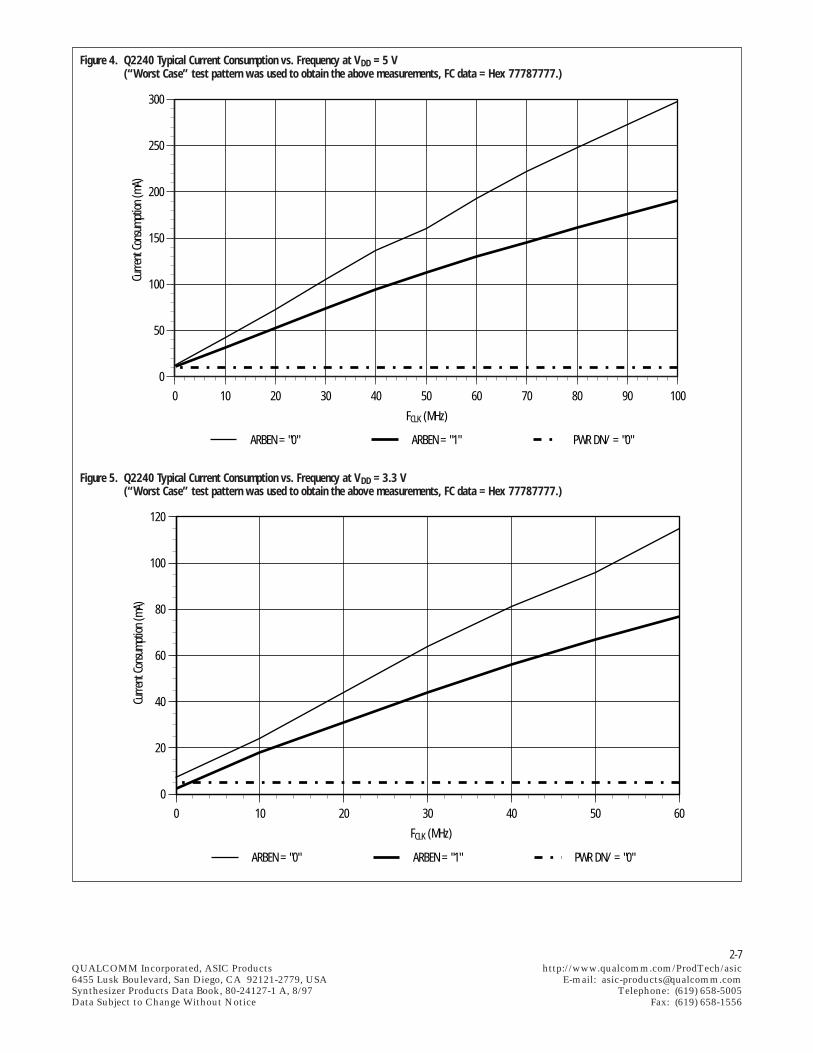
ARBITRARY WAVEFORM MODEIn addition to standard sine wave generation, the
Q2240I-2S1 and -3S1 are designed to provide a sine
lookup bypass function which will output the upper
bits of the phase accumulator directly instead of being
mapped into and through the sine LUT. This allows
the Q2240 to form the basis of an arbitrary waveform
generator. When used in this mode, general waveform
mapping can be accomplished using an external RAM
or RAMDAC that is loaded with the desired sampled
signal. The Arbitrary Waveform Mode is enabled when
the ARBEN input is set to a logic “High”. When
activated, this function will direct the 14 MSB output
bits of the phase accumulator directly as the DDS
digital outputs (OUT0 - OUT 13). In this case, the
unused sine LUT is deactivated internally to reduce the
overall Q2240 current consumption, as seen in the
comparative measurements shown in Figures 4 and 5.
All DDS control functions remain equally valid during
operation for standard sine wave generation or in
Arbitrary Waveform Mode with the exception that the
output format selection does not apply since the binary
coding options are only for the sine amplitude output.
Output pins OUT12 and OUT13 are dedicated output
signals used in Arbitrary Waveform Mode only and
remain inactive to reduce switching noise when this
mode is disabled by setting the ARBEN input to “Low”.
POWER-DOWN MODEThe Q2240I-2S1 and -3S1 provide a Power-down Mode
to minimize power consumption when the DDS is not
in use. The Power-down Mode is enabled when the
input signal PWR DN/ is set to a logic “Low”. The
2-7QUALCOMM Incorporated, ASIC Products http://www.qualcomm.com/ProdTech/asic6455 Lusk Boulevard, San Diego, CA 92121-2779, USA E-mail: [email protected] Products Data Book, 80-24127-1 A, 8/97 Telephone: (619) 658-5005Data Subject to Change Without Notice Fax: (619) 658-1556
Figure 4. Q2240 Typical Current Consumption vs. Frequency at VDD = 5 V (“Worst Case” test pattern was used to obtain the above measurements, FC data = Hex 77787777.)
0
50
100
150
200
250
300
0 10 20 30 40 50 60 70 80 90 100
Curre
nt Co
nsum
ption
(mA)
FCLK (MHz)
ARBEN = "0" ARBEN = "1" PWR DN/ = "0"
Figure 5. Q2240 Typical Current Consumption vs. Frequency at VDD = 3.3 V (“Worst Case” test pattern was used to obtain the above measurements, FC data = Hex 77787777.)
0
20
40
60
80
100
120
0 10 20 30 40 50 60
Curre
nt Co
nsum
ption
(mA)
FCLK (MHz)
ARBEN = "0" ARBEN = "1" PWR DN/ = "0"
2-8QUALCOMM Incorporated, ASIC Products http://www.qualcomm.com/ProdTech/asic6455 Lusk Boulevard, San Diego, CA 92121-2779, USA E-mail: [email protected] Products Data Book, 80-24127-1 A, 8/97 Telephone: (619) 658-5005Data Subject to Change Without Notice Fax: (619) 658-1556
PWR DN/ control is a static signal and asynchronous to
any clock input. The DDS is kept in a power-down
condition as long as PWR DN/ is enabled causing
current consumption to be reduced to within 10 mA or
less (see Figures 4 and 5 for typical current
consumption measurements). Internally, the PWR DN/
signal is synchronized to the input signal SYS CLK to
guarantee there will be phase continuity going into and
coming out of Power-down Mode. When power-down
is activated, all internal registers will retain their
values prior to power-down and the active digitized
output value will freeze at the DDS outputs. This
means that when power-down is disabled and the DDS
is activated to a power-up condition, previous phase
continuity will be maintained, even with the given
latency effect to the DDS outputs. Additionally, the
reset function (RESET/) can be used while in Power-
down Mode, if desired.
RESETA reset function is provided for all Q2240 versions to
allow all output signals and internal registers to be
cleared. Reset is enabled when the input signal RESET/
is set to a logic “Low”. The RESET/ control is a static
signal and asynchronous to any clock input. The
RESET/ should not be left in a floating condition. If
unused, connect the RESET/ signal to a “High” setting
through a pull-up resistor to VDD to ensure that the
device does not hang in a reset state (typical pull-up
resistor values are between 5 kΩ to 20 kΩ). When the
reset function is activated, the FC Register, Serial
Buffer, Phase Accumulator, Sine LUT, and Output are
set to “0”. The DDS output will remain at the reset
level until RESET/ is disabled by setting to a logic
“High”. When RESET/ is disabled, the Q2240 can be
loaded with a new FC value immediately and the
accumulation process will begin again. The DDS
output will be at “0” until valid outputs are available at
the output registers after a fixed latency (see Timing
Specifications section).
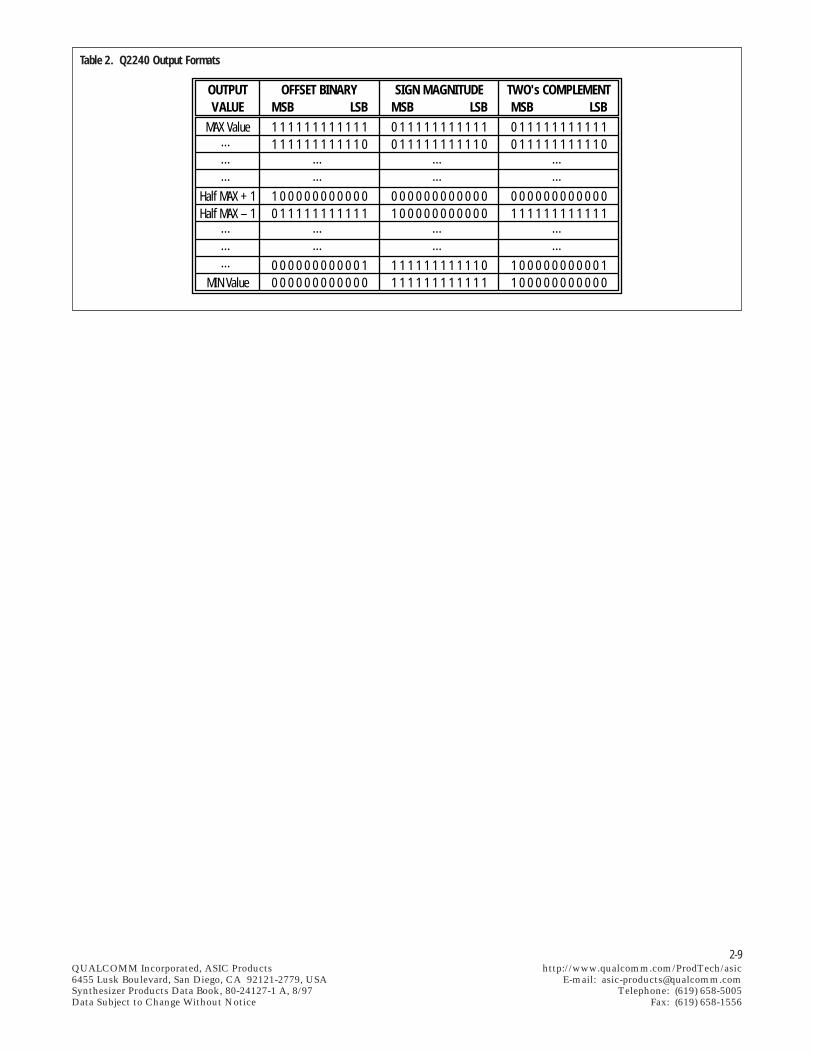
OUTPUT FORMATFor the Q2240I-1N, output format selection of the sine
amplitude output is provided to support either Offset
Binary or Offset Two’s Complement binary coding.
The amplitude output is formatted using Offset Binary
notation when the input signal OBN is set to a logic
“High”. When OBN is set “Low”, the output format is
Offset Two’s Complement.
For the Q2240I-2S1 and -3S1, output format
selection of the sine amplitude output is provided to
support either Offset Binary, Offset Sign Magnitude, or
Offset Two’s Complement binary coding. The output
format is selected depending on the settings of the
input signals OBN and SIGN MAG as follows:
OBN = “High”, SIGN MAG = “Low” :
Selects Offset Binary
OBN = “Low”, SIGN MAG = “High” :
Selects Offset Sign Magnitude
OBN = “Low”, SIGN MAG = “Low” :
Selects Offset Two’s Complement
OBN = “High”, SIGN MAG = “High” :
Selects Offset Two’s Complement
Table 2 shows the effect of the output format for
output signals OUT [11:0].
2-9QUALCOMM Incorporated, ASIC Products http://www.qualcomm.com/ProdTech/asic6455 Lusk Boulevard, San Diego, CA 92121-2779, USA E-mail: [email protected] Products Data Book, 80-24127-1 A, 8/97 Telephone: (619) 658-5005Data Subject to Change Without Notice Fax: (619) 658-1556
Table 2. Q2240 Output Formats
OUTPUTVALUE
MAX Value………
Half MAX + 1Half MAX – 1
………
MIN Value
OFFSET BINARY
1 1 1 1 1 1 1 1 1 1 1 11 1 1 1 1 1 1 1 1 1 1 0
……
1 0 0 0 0 0 0 0 0 0 0 00 1 1 1 1 1 1 1 1 1 1 1
……
0 0 0 0 0 0 0 0 0 0 0 10 0 0 0 0 0 0 0 0 0 0 0
TWO's COMPLEMENT
0 1 1 1 1 1 1 1 1 1 1 10 1 1 1 1 1 1 1 1 1 1 0
……
0 0 0 0 0 0 0 0 0 0 0 01 1 1 1 1 1 1 1 1 1 1 1
……
1 0 0 0 0 0 0 0 0 0 0 11 0 0 0 0 0 0 0 0 0 0 0
LSBMSBSIGN MAGNITUDE
0 1 1 1 1 1 1 1 1 1 1 10 1 1 1 1 1 1 1 1 1 1 0
……
0 0 0 0 0 0 0 0 0 0 0 01 0 0 0 0 0 0 0 0 0 0 0
……
1 1 1 1 1 1 1 1 1 1 1 01 1 1 1 1 1 1 1 1 1 1 1
LSBMSB LSBMSB
2-10QUALCOMM Incorporated, ASIC Products http://www.qualcomm.com/ProdTech/asic6455 Lusk Boulevard, San Diego, CA 92121-2779, USA E-mail: [email protected] Products Data Book, 80-24127-1 A, 8/97 Telephone: (619) 658-5005Data Subject to Change Without Notice Fax: (619) 658-1556
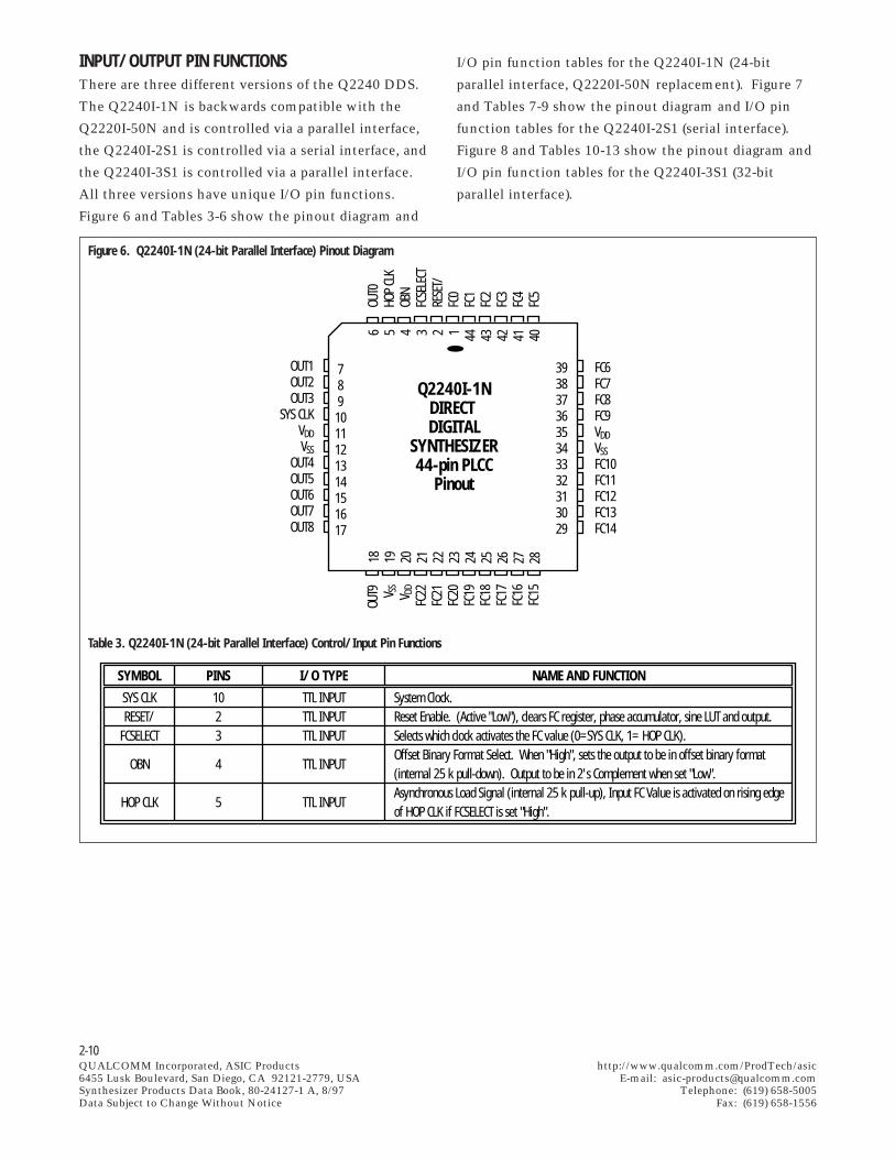
INPUT/OUTPUT PIN FUNCTIONSThere are three different versions of the Q2240 DDS.
The Q2240I-1N is backwards compatible with the
Q2220I-50N and is controlled via a parallel interface,
the Q2240I-2S1 is controlled via a serial interface, and
the Q2240I-3S1 is controlled via a parallel interface.
All three versions have unique I/O pin functions.
Figure 6 and Tables 3-6 show the pinout diagram and
3938373635343332313029
7891011121314151617
6 5 4 3 2 1 44 43 42 41 40
18 19 20 21 22 23 24 25 26 27 28
FC6FC7FC8FC9VDDVSSFC10FC11FC12FC13FC14
OUT1OUT2OUT3
SYS CLKVDDVSS
OUT4OUT5OUT6OUT7OUT8
OUT9 V S
SV D
DFC
22FC
21FC
20FC
19FC
18FC
17FC
16FC
15
OUT0
HOP
CLK
OBN
FCSE
LECT
RESE
T/FC
0FC
1FC
2FC
3FC
4FC
5
Q2240I-1NDIRECT DIGITAL
SYNTHESIZER44-pin PLCC
Pinout
Figure 6. Q2240I-1N (24-bit Parallel Interface) Pinout Diagram
SYMBOL
SYS CLKRESET/
FCSELECT
OBN
HOP CLK
PINS
1023
4
5
I/O TYPE
TTL INPUTTTL INPUTTTL INPUT
TTL INPUT
TTL INPUT
NAME AND FUNCTION
System Clock.Reset Enable. (Active "Low"), clears FC register, phase accumulator, sine LUT and output.Selects which clock activates the FC value (0=SYS CLK, 1= HOP CLK).Offset Binary Format Select. When "High", sets the output to be in offset binary format(internal 25 k pull-down). Output to be in 2's Complement when set "Low".Asynchronous Load Signal (internal 25 k pull-up), Input FC Value is activated on rising edgeof HOP CLK if FCSELECT is set "High".
Table 3. Q2240I-1N (24-bit Parallel Interface) Control/Input Pin Functions
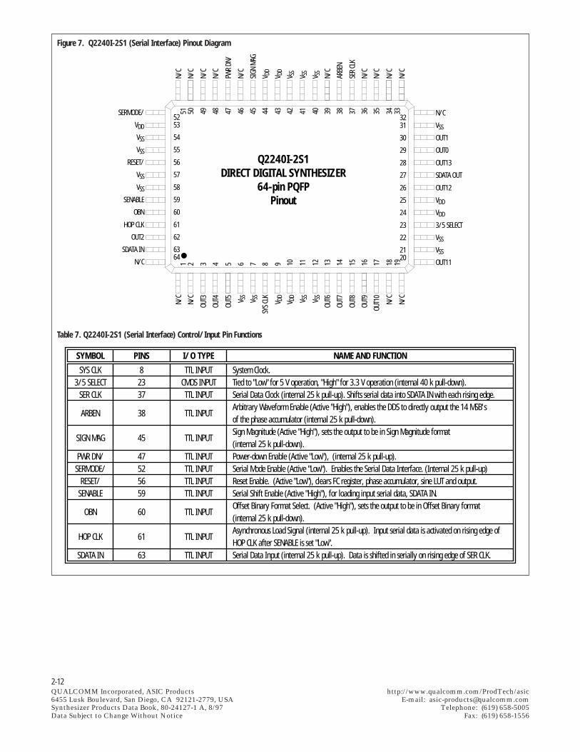
I/O pin function tables for the Q2240I-1N (24-bit
parallel interface, Q2220I-50N replacement). Figure 7
and Tables 7-9 show the pinout diagram and I/O pin
function tables for the Q2240I-2S1 (serial interface).
Figure 8 and Tables 10-13 show the pinout diagram and
I/O pin function tables for the Q2240I-3S1 (32-bit
parallel interface).
2-11QUALCOMM Incorporated, ASIC Products http://www.qualcomm.com/ProdTech/asic6455 Lusk Boulevard, San Diego, CA 92121-2779, USA E-mail: [email protected] Products Data Book, 80-24127-1 A, 8/97 Telephone: (619) 658-5005Data Subject to Change Without Notice Fax: (619) 658-1556
Table 4. Q2240I-1N (24-bit Parallel Interface) Frequency Control Pin Functions
SYMBOL
FC0FC1FC2FC3FC4FC5FC6FC7FC8FC9FC10FC11FC12FC13FC14FC15FC16FC17FC18FC19FC20FC21FC22
PINS
144434241403938373633323130292827262524232221
I/O TYPE
TTL INPUTTTL INPUTTTL INPUTTTL INPUTTTL INPUTTTL INPUTTTL INPUTTTL INPUTTTL INPUTTTL INPUTTTL INPUTTTL INPUTTTL INPUTTTL INPUTTTL INPUTTTL INPUTTTL INPUTTTL INPUTTTL INPUTTTL INPUTTTL INPUTTTL INPUTTTL INPUT
NAME AND FUNCTION
Frequency Control Bit 0 (LSB) (Internal 25 k Pull-up)Frequency Control Bit 1 (Internal 25 k Pull-up)Frequency Control Bit 2 (Internal 25 k Pull-up)Frequency Control Bit 3 (Internal 25 k Pull-up)Frequency Control Bit 4 (Internal 25 k Pull-up)Frequency Control Bit 5 (Internal 25 k Pull-up)Frequency Control Bit 6 (Internal 25 k Pull-up)Frequency Control Bit 7 (Internal 25 k Pull-up)Frequency Control Bit 8 (Internal 25 k Pull-up)Frequency Control Bit 9 (Internal 25 k Pull-up)Frequency Control Bit 10 (Internal 25 k Pull-up)Frequency Control Bit 11 (Internal 25 k Pull-up)Frequency Control Bit 12 (Internal 25 k Pull-up)Frequency Control Bit 13 (Internal 25 k Pull-up)Frequency Control Bit 14 (Internal 25 k Pull-up)Frequency Control Bit 15 (Internal 25 k Pull-up)Frequency Control Bit 16 (Internal 25 k Pull-up)Frequency Control Bit 17 (Internal 25 k Pull-up)Frequency Control Bit 18 (Internal 25 k Pull-up)Frequency Control Bit 19 (Internal 25 k Pull-up)Frequency Control Bit 20 (Internal 25 k Pull-up)Frequency Control Bit 21 (Internal 25 k Pull-up)Frequency Control Bit 22 (Internal 25 k Pull-up)
Table 5. Q2240I-1N (24-bit Parallel Interface) Data Output Pin Functions
SYMBOL
OUT0OUT1OUT2OUT3OUT4OUT5OUT6OUT7OUT8OUT9
*±8 mA drive strength at VDD = 5.0 V (± 10%).
PINS
6789131415161718
I/O TYPE*
CMOS OUTPUTCMOS OUTPUTCMOS OUTPUTCMOS OUTPUTCMOS OUTPUTCMOS OUTPUTCMOS OUTPUTCMOS OUTPUTCMOS OUTPUTCMOS OUTPUT
NAME AND FUNCTION
Data OUTPUT Bit 0 (LSB)Data OUTPUT Bit 1Data OUTPUT Bit 2Data OUTPUT Bit 3Data OUTPUT Bit 4Data OUTPUT Bit 5Data OUTPUT Bit 6Data OUTPUT Bit 7Data OUTPUT Bit 8Data OUTPUT Bit 9
Table 6. Q2240I-1N (24-bit Parallel Interface) Voltage Supply Pin Functions
SYMBOL
VDD
VSS
PINS
11, 20, 3512, 19, 34
I/O TYPE
PWRGND
NAME AND FUNCTION
Power (+ 5 VDC )Ground
2-12QUALCOMM Incorporated, ASIC Products http://www.qualcomm.com/ProdTech/asic6455 Lusk Boulevard, San Diego, CA 92121-2779, USA E-mail: [email protected] Products Data Book, 80-24127-1 A, 8/97 Telephone: (619) 658-5005Data Subject to Change Without Notice Fax: (619) 658-1556
Figure 7. Q2240I-2S1 (Serial Interface) Pinout Diagram
1 2 3 4 5 6 7 8 9 10 11 12 13 14 15 16 17 18 19
N/C
N/C
50 49 48 47 46 45 44 43 42 41 40 39 38 37 36 35 34 3351N/
C
N/C
N/C
PWR
DN/
N/C
SIGN
MAG
V DD
V DD
V SS
V SS
V SS
N/C
ARBE
N
SER
CLK
N/C
N/C
N/C
N/C
N/C
5253
54
55
56
57
58
59
60
61
62
6364
VDD VSS
OUT1
OUT0
OUT13
SDATA OUT
OUT12
VDD
VDD
3/5 SELECT
VSS
VSS
OUT11
30
29
28
27
26
25
24
23
22
2120
31
N/C32
VSS
VSS
RESET/
VSS
VSS
SENABLE
OBN
HOP CLK
OUT2
SDATA IN
N/C
SERMODE/
OUT3
OUT4
OUT5 V S
S
V SS
SYS C
LK V DD
V DD
V SS
V SS
OUT6
OUT7
OUT8
OUT9
OUT1
0
N/C
N/C
Q2240I-2S1DIRECT DIGITAL SYNTHESIZER
64-pin PQFPPinout
Table 7. Q2240I-2S1 (Serial Interface) Control/Input Pin Functions
SYMBOL
SYS CLK3/5 SELECT
SER CLK
ARBEN
SIGN MAG
PWR DN/SERMODE/
RESET/SENABLE
OBN
HOP CLK
SDATA IN
PINS
82337
38
45
47525659
60
61
63
I/O TYPE
TTL INPUTCMOS INPUTTTL INPUT
TTL INPUT
TTL INPUT
TTL INPUTTTL INPUTTTL INPUTTTL INPUT
TTL INPUT
TTL INPUT
TTL INPUT
NAME AND FUNCTION
System Clock.Tied to "Low" for 5 V operation, "High" for 3.3 V operation (internal 40 k pull-down).Serial Data Clock (internal 25 k pull-up). Shifts serial data into SDATA IN with each rising edge.Arbitrary Waveform Enable (Active "High"), enables the DDS to directly output the 14 MSB'sof the phase accumulator (internal 25 k pull-down). Sign Magnitude (Active "High"), sets the output to be in Sign Magnitude format(internal 25 k pull-down).Power-down Enable (Active "Low"), (internal 25 k pull-up).Serial Mode Enable (Active "Low"). Enables the Serial Data Interface. (Internal 25 k pull-up)Reset Enable. (Active "Low"), clears FC register, phase accumulator, sine LUT and output.Serial Shift Enable (Active "High"), for loading input serial data, SDATA IN.Offset Binary Format Select. (Active "High"), sets the output to be in Offset Binary format(internal 25 k pull-down).Asynchronous Load Signal (internal 25 k pull-up). Input serial data is activated on rising edge of HOP CLK after SENABLE is set "Low".Serial Data Input (internal 25 k pull-up). Data is shifted in serially on rising edge of SER CLK.
2-13QUALCOMM Incorporated, ASIC Products http://www.qualcomm.com/ProdTech/asic6455 Lusk Boulevard, San Diego, CA 92121-2779, USA E-mail: [email protected] Products Data Book, 80-24127-1 A, 8/97 Telephone: (619) 658-5005Data Subject to Change Without Notice Fax: (619) 658-1556
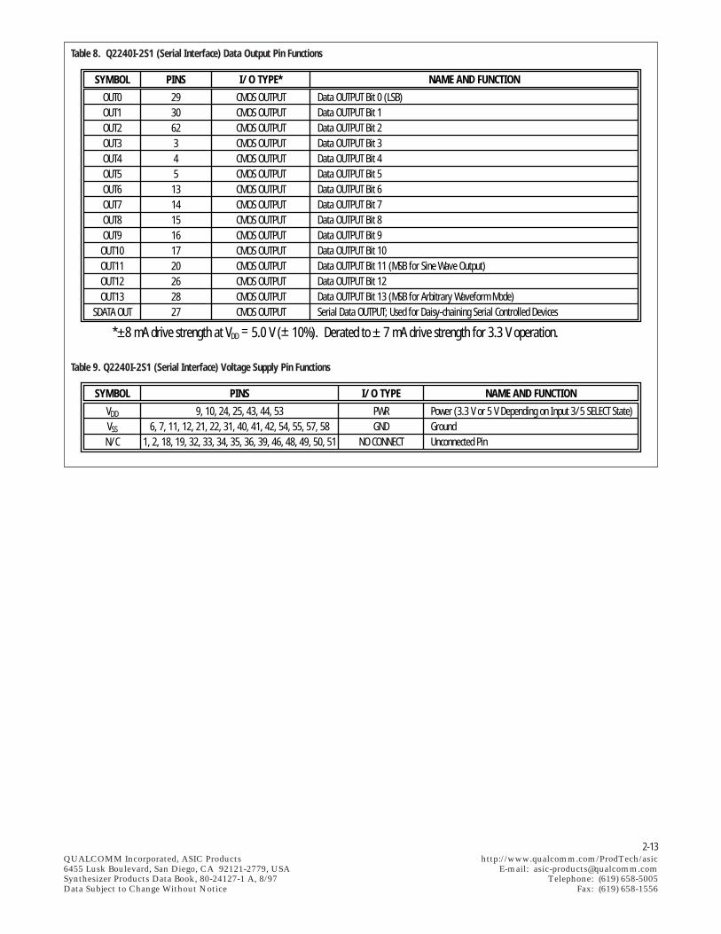
Table 8. Q2240I-2S1 (Serial Interface) Data Output Pin Functions
SYMBOL
OUT0OUT1OUT2OUT3OUT4OUT5OUT6OUT7OUT8OUT9OUT10OUT11OUT12OUT13
SDATA OUT
*±8 mA drive strength at VDD = 5.0 V (± 10%). Derated to ± 7 mA drive strength for 3.3 V operation.
PINS
293062345131415161720262827
I/O TYPE*
CMOS OUTPUTCMOS OUTPUTCMOS OUTPUTCMOS OUTPUTCMOS OUTPUTCMOS OUTPUTCMOS OUTPUTCMOS OUTPUTCMOS OUTPUTCMOS OUTPUTCMOS OUTPUTCMOS OUTPUTCMOS OUTPUTCMOS OUTPUTCMOS OUTPUT
NAME AND FUNCTION
Data OUTPUT Bit 0 (LSB)Data OUTPUT Bit 1Data OUTPUT Bit 2Data OUTPUT Bit 3Data OUTPUT Bit 4Data OUTPUT Bit 5Data OUTPUT Bit 6Data OUTPUT Bit 7Data OUTPUT Bit 8Data OUTPUT Bit 9Data OUTPUT Bit 10Data OUTPUT Bit 11 (MSB for Sine Wave Output)Data OUTPUT Bit 12Data OUTPUT Bit 13 (MSB for Arbitrary Waveform Mode)Serial Data OUTPUT; Used for Daisy-chaining Serial Controlled Devices
Table 9. Q2240I-2S1 (Serial Interface) Voltage Supply Pin Functions
SYMBOL
VDD
VSS
N/C
PINS
9, 10, 24, 25, 43, 44, 536, 7, 11, 12, 21, 22, 31, 40, 41, 42, 54, 55, 57, 58
1, 2, 18, 19, 32, 33, 34, 35, 36, 39, 46, 48, 49, 50, 51
I/O TYPE
PWRGND
NO CONNECT
NAME AND FUNCTION
Power (3.3 V or 5 V Depending on Input 3/5 SELECT State)GroundUnconnected Pin
2-14QUALCOMM Incorporated, ASIC Products http://www.qualcomm.com/ProdTech/asic6455 Lusk Boulevard, San Diego, CA 92121-2779, USA E-mail: [email protected] Products Data Book, 80-24127-1 A, 8/97 Telephone: (619) 658-5005Data Subject to Change Without Notice Fax: (619) 658-1556
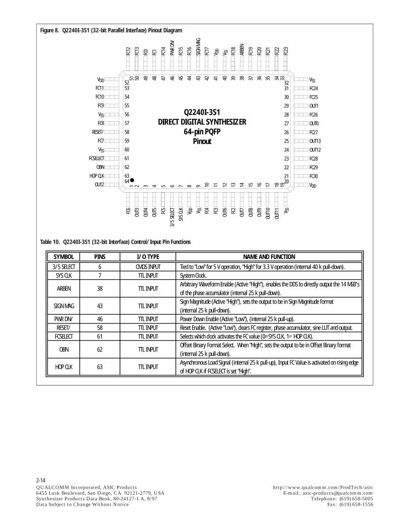
Figure 8. Q2240I-3S1 (32-bit Parallel Interface) Pinout Diagram
1 2 3 4 5 6 7 8 9 10 11 12 13 14 15 16 17 18 19
FC6
OUT3
50 49 48 47 46 45 44 43 42 41 40 39 38 37 36 35 34 3351FC
13
FC0
FC1
FC14
PWR
DN/
FC15
FC16
SIGN
MAG
FC17
V DD
V SS
FC18
ARBE
N
FC19
FC20
FC21
FC22
FC23
FC12
5253
54
55
56
57
58
59
60
61
62
6364
FC11 FC24
FC25
OUT1
FC26
OUT0
FC27
OUT13
OUT12
FC28
FC29
FC30
VDD
30
29
28
27
26
25
24
23
22
2120
31
VSS32
FC10
FC9
VSS
FC8
RESET/
FC7
VSS
FCSELECT
OBN
HOP CLK
OUT2
VDD
OUT4
OUT5 FC5
3/5
SELE
CT
SYS C
LK V DD
V SS
FC4
FC3
OUT6 FC2
OUT7
OUT8
OUT9
OUT1
0
OUT1
1
V SS
Q2240I-3S1DIRECT DIGITAL SYNTHESIZER
64-pin PQFPPinout
Table 10. Q2240I-3S1 (32-bit Interface) Control/Input Pin Functions
SYMBOL
3/5 SELECTSYS CLK
ARBEN
SIGN MAG
PWR DN/RESET/
FCSELECT
OBN
HOP CLK
PINS
67
38
43
465861
62
63
I/O TYPE
CMOS INPUTTTL INPUT
TTL INPUT
TTL INPUT
TTL INPUTTTL INPUTTTL INPUT
TTL INPUT
TTL INPUT
NAME AND FUNCTION
Tied to "Low" for 5 V operation, "High" for 3.3 V operation (internal 40 k pull-down).System Clock.Arbitrary Waveform Enable (Active "High"), enables the DDS to directly output the 14 MSB'sof the phase accumulator (internal 25 k pull-down).Sign Magnitude (Active "High"), sets the output to be in Sign Magnitude format(internal 25 k pull-down).Power Down Enable (Active "Low"), (internal 25 k pull-up).Reset Enable. (Active "Low"), clears FC register, phase accumulator, sine LUT and output.Selects which clock activates the FC value (0=SYS CLK, 1= HOP CLK).Offset Binary Format Select. When "High", sets the output to be in Offset Binary format(internal 25 k pull-down).Asynchronous Load Signal (internal 25 k pull-up), Input FC Value is activated on rising edgeof HOP CLK if FCSELECT is set "High".
2-15QUALCOMM Incorporated, ASIC Products http://www.qualcomm.com/ProdTech/asic6455 Lusk Boulevard, San Diego, CA 92121-2779, USA E-mail: [email protected] Products Data Book, 80-24127-1 A, 8/97 Telephone: (619) 658-5005Data Subject to Change Without Notice Fax: (619) 658-1556
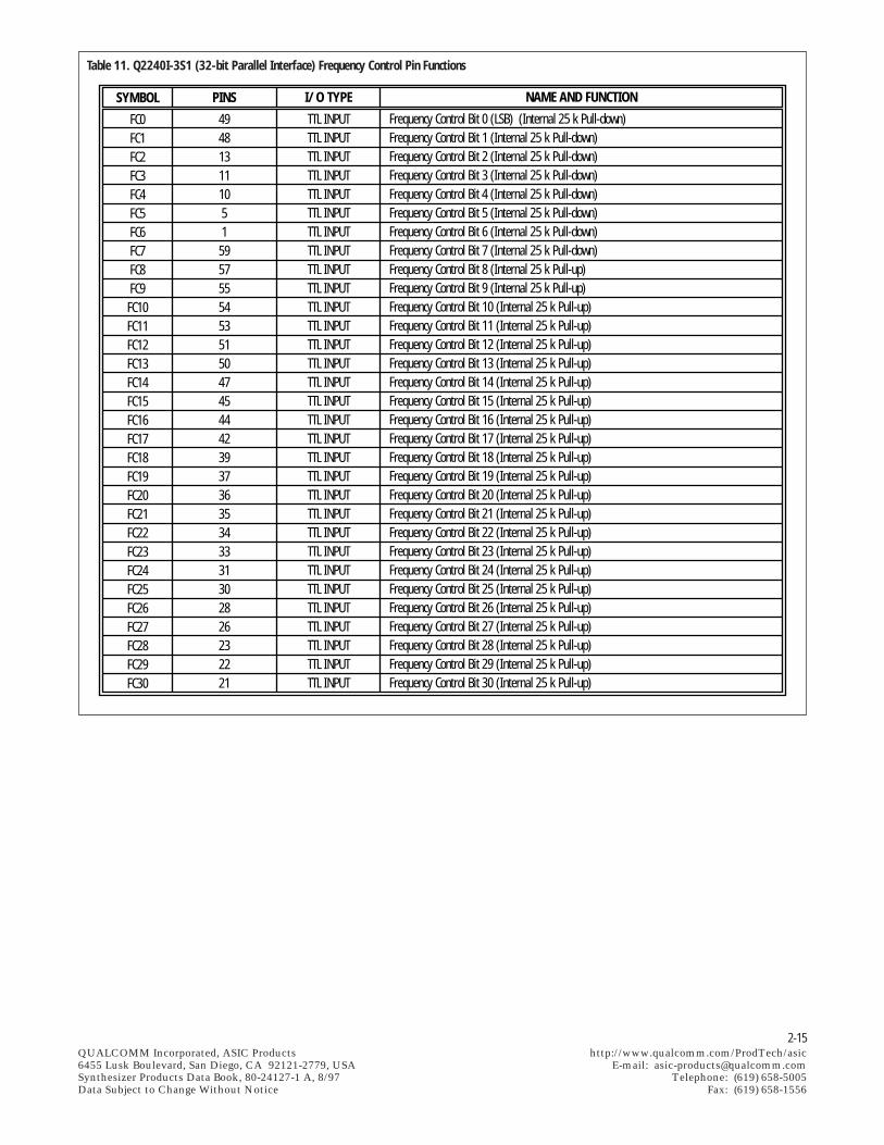
Table 11. Q2240I-3S1 (32-bit Parallel Interface) Frequency Control Pin Functions
SYMBOL
FC0FC1FC2FC3FC4FC5FC6FC7FC8FC9FC10FC11FC12FC13FC14FC15FC16FC17FC18FC19FC20FC21FC22FC23FC24FC25FC26FC27FC28FC29FC30
PINS
494813111051595755545351504745444239373635343331302826232221
I/O TYPE
TTL INPUTTTL INPUTTTL INPUTTTL INPUTTTL INPUTTTL INPUTTTL INPUTTTL INPUTTTL INPUTTTL INPUTTTL INPUTTTL INPUTTTL INPUTTTL INPUTTTL INPUTTTL INPUTTTL INPUTTTL INPUTTTL INPUTTTL INPUTTTL INPUTTTL INPUTTTL INPUTTTL INPUTTTL INPUTTTL INPUTTTL INPUTTTL INPUTTTL INPUTTTL INPUTTTL INPUT
NAME AND FUNCTION
Frequency Control Bit 0 (LSB) (Internal 25 k Pull-down)Frequency Control Bit 1 (Internal 25 k Pull-down)Frequency Control Bit 2 (Internal 25 k Pull-down)Frequency Control Bit 3 (Internal 25 k Pull-down)Frequency Control Bit 4 (Internal 25 k Pull-down)Frequency Control Bit 5 (Internal 25 k Pull-down)Frequency Control Bit 6 (Internal 25 k Pull-down)Frequency Control Bit 7 (Internal 25 k Pull-down)Frequency Control Bit 8 (Internal 25 k Pull-up)Frequency Control Bit 9 (Internal 25 k Pull-up)Frequency Control Bit 10 (Internal 25 k Pull-up)Frequency Control Bit 11 (Internal 25 k Pull-up)Frequency Control Bit 12 (Internal 25 k Pull-up)Frequency Control Bit 13 (Internal 25 k Pull-up)Frequency Control Bit 14 (Internal 25 k Pull-up)Frequency Control Bit 15 (Internal 25 k Pull-up)Frequency Control Bit 16 (Internal 25 k Pull-up)Frequency Control Bit 17 (Internal 25 k Pull-up)Frequency Control Bit 18 (Internal 25 k Pull-up)Frequency Control Bit 19 (Internal 25 k Pull-up)Frequency Control Bit 20 (Internal 25 k Pull-up)Frequency Control Bit 21 (Internal 25 k Pull-up)Frequency Control Bit 22 (Internal 25 k Pull-up)Frequency Control Bit 23 (Internal 25 k Pull-up)Frequency Control Bit 24 (Internal 25 k Pull-up)Frequency Control Bit 25 (Internal 25 k Pull-up)Frequency Control Bit 26 (Internal 25 k Pull-up)Frequency Control Bit 27 (Internal 25 k Pull-up)Frequency Control Bit 28 (Internal 25 k Pull-up)Frequency Control Bit 29 (Internal 25 k Pull-up)Frequency Control Bit 30 (Internal 25 k Pull-up)
2-16QUALCOMM Incorporated, ASIC Products http://www.qualcomm.com/ProdTech/asic6455 Lusk Boulevard, San Diego, CA 92121-2779, USA E-mail: [email protected] Products Data Book, 80-24127-1 A, 8/97 Telephone: (619) 658-5005Data Subject to Change Without Notice Fax: (619) 658-1556
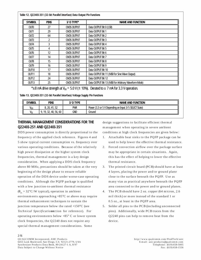
Table 12. Q2240I-3S1 (32-bit Parallel Interface) Data Output Pin Functions
Table 13. Q2240I-3S1 (32-bit Parallel Interface) Voltage Supply Pin Functions
SYMBOL
OUT0OUT1OUT2OUT3OUT4OUT5OUT6OUT7OUT8OUT9OUT10OUT11OUT12OUT13
*±8 mA drive strength at VDD = 5.0 V (± 10%). Derated to ± 7 mA for 3.3 V operation.
PINS
2729642341214151617182425
I/O TYPE*
CMOS OUTPUTCMOS OUTPUTCMOS OUTPUTCMOS OUTPUTCMOS OUTPUTCMOS OUTPUTCMOS OUTPUTCMOS OUTPUTCMOS OUTPUTCMOS OUTPUTCMOS OUTPUTCMOS OUTPUTCMOS OUTPUTCMOS OUTPUT
NAME AND FUNCTION
Data OUTPUT Bit 0 (LSB)Data OUTPUT Bit 1Data OUTPUT Bit 2Data OUTPUT Bit 3Data OUTPUT Bit 4Data OUTPUT Bit 5Data OUTPUT Bit 6Data OUTPUT Bit 7Data OUTPUT Bit 8Data OUTPUT Bit 9Data OUTPUT Bit 10Data OUTPUT Bit 11 (MSB for Sine Wave Output)Data OUTPUT Bit 12Data OUTPUT Bit 13 (MSB for Arbitrary Waveform Mode)
SYMBOL
VDD
VSS
PINS
8, 20, 41, 529, 19, 32, 40, 56, 60
I/O TYPE
PWRGND
NAME AND FUNCTION
Power (3.3 or 5 V Depending on Input 3/5 SELECT State)Ground
THERMAL MANAGEMENT CONSIDERATIONS FOR THEQ2240I-2S1 AND Q2240I-3S1DDS power consumption is directly proportional to the
frequency of the applied clock reference. Figures 4 and
5 show typical current consumption vs. frequency over
various operating conditions. Because of the relatively
high power dissipation at the higher system clock
frequencies, thermal management is a key design
consideration. When applying a DDS clock frequency
above 80 MHz, precautions should be taken at the very
beginning of the design phase to ensure reliable
operation of the DDS device under worse-case operating
conditions. Although the PQFP package is qualified
with a low junction-to-ambient thermal resistance
(θJA = 32°C/W typical), operation in ambient
environments approaching +85°C or above may require
thermal enhancement techniques to sustain the
junction temperature below the rated +150°C (see
Technical Specifications section for reference). For
operating environments below +85° C or lower system
clock frequencies, the Q2240 does not require any
special thermal management considerations. Some
design suggestions to facilitate efficient thermal
management when operating in severe ambient
conditions at high clock frequencies are given below:
1. Attachable heat sinks to the PQFP package can be
used to help lower the effective thermal resistance.
2. Forced convection airflow over the package surface
may be appropriate in certain situations. Again,
this has the effect of helping to lower the effective
thermal resistance.
3. The printed circuit board (PCB) should have at least
4 layers, placing the power and/or ground plane
close to the surface beneath the PQFP. Use as
many vias as practical anywhere beneath the PQFP
area connected to the power and/or ground planes.
4. The PCB should have 2 oz. copper (64 micron, 2.6
mil thick) or more instead of the standard 1 or
0.5 oz., at least in the PQFP area.
5. Solder all pins to the PCB (including unconnected
pins). Additionally, wide PCB traces from the
Q2240 pins can help to remove heat from the
device.
2-17QUALCOMM Incorporated, ASIC Products http://www.qualcomm.com/ProdTech/asic6455 Lusk Boulevard, San Diego, CA 92121-2779, USA E-mail: [email protected] Products Data Book, 80-24127-1 A, 8/97 Telephone: (619) 658-5005Data Subject to Change Without Notice Fax: (619) 658-1556
6. Thermally conductive, electrically isolated epoxy
or other thermal interface material placed beneath
the PQFP before reflow attach can significantly
improve thermal coupling with the PCB.
7. Total thermal load from other components or
materials in the area of the PQFP should be
minimized.
8. Place the PQFP near a large thermal mass such as a
PCB edge connector, for example. This has the
effect of being an indirect heat sink mass for the
dissipating power.
9. Thermal “Pillows” are available to be placed on hot
components and conduct heat to other surfaces,
such as a metal case.
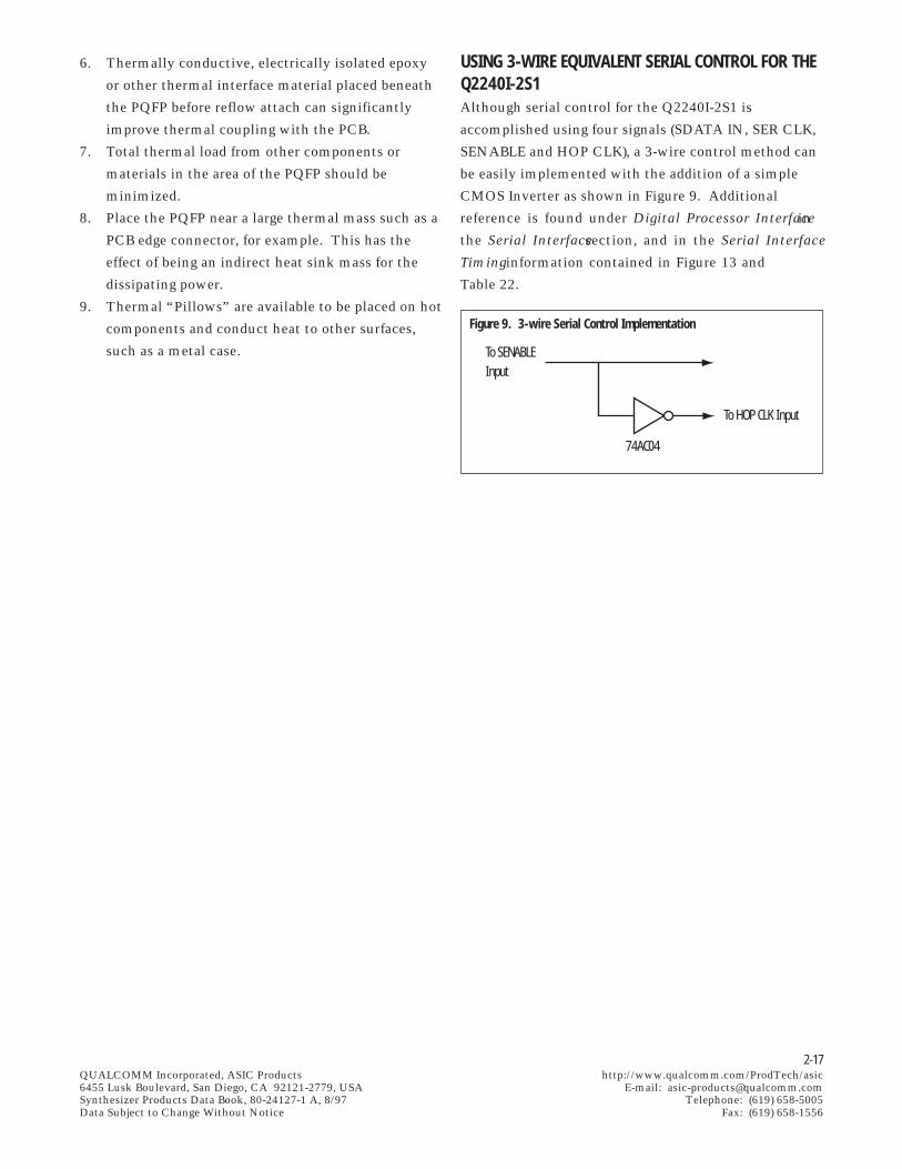
USING 3-WIRE EQUIVALENT SERIAL CONTROL FOR THEQ2240I-2S1Although serial control for the Q2240I-2S1 is
accomplished using four signals (SDATA IN, SER CLK,
SENABLE and HOP CLK), a 3-wire control method can
be easily implemented with the addition of a simple
CMOS Inverter as shown in Figure 9. Additional
reference is found under Digital Processor Interface in
the Serial Interface section, and in the Serial Interface
Timing information contained in Figure 13 and
Table 22.
Figure 9. 3-wire Serial Control Implementation
To SENABLEInput
74AC04
To HOP CLK Input
2-18QUALCOMM Incorporated, ASIC Products http://www.qualcomm.com/ProdTech/asic6455 Lusk Boulevard, San Diego, CA 92121-2779, USA E-mail: [email protected] Products Data Book, 80-24127-1 A, 8/97 Telephone: (619) 658-5005Data Subject to Change Without Notice Fax: (619) 658-1556
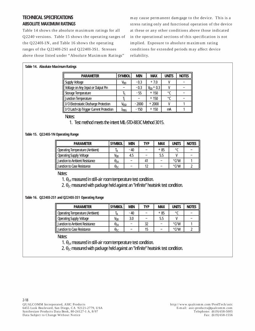
TECHNICAL SPECIFICATIONSABSOLUTE MAXIMUM RATINGSTable 14 shows the absolute maximum ratings for all
Q2240 versions. Table 15 shows the operating ranges of
the Q2240I-1N, and Table 16 shows the operating
ranges of the Q2240I-2S1 and Q2240I-3S1. Stresses
above those listed under “Absolute Maximum Ratings”
may cause permanent damgage to the device. This is a
stress rating only and functional operation of the device
at these or any other conditions above those indicated
in the operational sections of this specification is not
implied. Exposure to absolute maximum rating
conditions for extended periods may affect device
reliability.
Table 14. Absolute Maximum Ratings
Supply VoltageVoltage on Any Input or Output PinStorage TemperatureJunction TemperatureI/O Electrostatic Discharge ProtectionI/O Latch-Up Trigger Current Protection
Notes: 1. Test method meets the intent MIL-STD-883C Method 3015.
PARAMETER SYMBOL
VDD
–TS
TJ
VESD
ITRIG
MIN- 0.3- 0.3- 55–
- 2000- 150
MAX+ 7.0
VDD + 0.3+ 150+ 150
+ 2000+ 150
UNITS
VV°C°CV
mA
NOTES––––11
Table 15. Q2240I-1N Operating Range
Operating Temperature (Ambient)Operating Supply VoltageJunction to Ambient ResistanceJunction to Case Resistance
Notes: 1. θJA measured in still-air room temperature test condition. 2. θJC measured with package held against an "infinite" heatsink test condition.
PARAMETER SYMBOL
TA
VDD
θJA
θJC
MIN- 404.5––
TYP––4112
MAX+ 855.5––
UNITS
°CV
°C/W°C/W
NOTES––12
Table 16. Q2240I-2S1 and Q2240I-3S1 Operating Range
Operating Temperature (Ambient)Operating Supply VoltageJunction to Ambient ResistanceJunction to Case Resistance
Notes: 1. θJA measured in still-air room temperature test condition. 2. θJC measured with package held against an "infinite" heatsink test condition.
PARAMETER SYMBOL
TA
VDD
θJA
θJC
MIN- 403.0––
TYP––3215
MAX+ 855.5––
UNITS
°CV
°C/W°C/W
NOTES––12
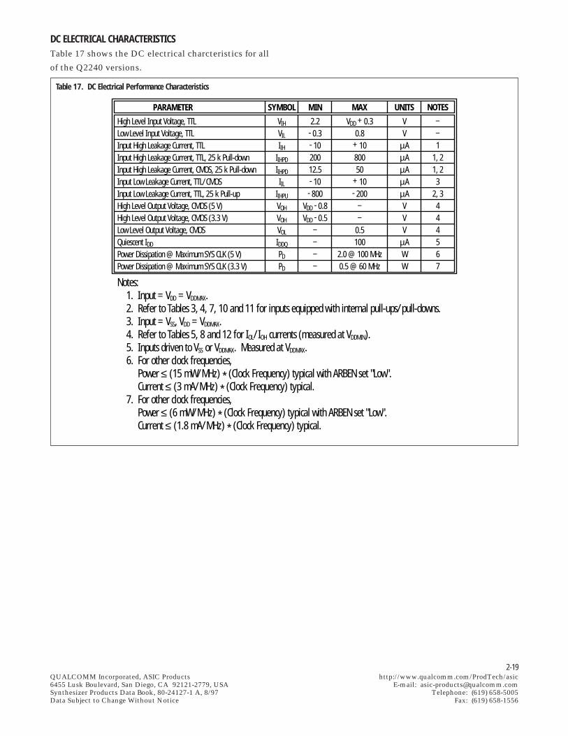
2-19QUALCOMM Incorporated, ASIC Products http://www.qualcomm.com/ProdTech/asic6455 Lusk Boulevard, San Diego, CA 92121-2779, USA E-mail: [email protected] Products Data Book, 80-24127-1 A, 8/97 Telephone: (619) 658-5005Data Subject to Change Without Notice Fax: (619) 658-1556
DC ELECTRICAL CHARACTERISTICSTable 17 shows the DC electrical charcteristics for all
of the Q2240 versions.
Table 17. DC Electrical Performance Characteristics
High Level Input Voltage, TTLLow Level Input Voltage, TTLInput High Leakage Current, TTLInput High Leakage Current, TTL, 25 k Pull-downInput High Leakage Current, CMOS, 25 k Pull-downInput Low Leakage Current, TTL/CMOSInput Low Leakage Current, TTL, 25 k Pull-upHigh Level Output Voltage, CMOS (5 V)High Level Output Voltage, CMOS (3.3 V)Low Level Output Voltage, CMOSQuiescent IDD
Power Dissipation @ Maximum SYS CLK (5 V)Power Dissipation @ Maximum SYS CLK (3.3 V)
Notes: 1. Input = VDD = VDDMAX. 2. Refer to Tables 3, 4, 7, 10 and 11 for inputs equipped with internal pull-ups/pull-downs. 3. Input = VSS, VDD = VDDMAX. 4. Refer to Tables 5, 8 and 12 for IOL/IOH currents (measured at VDDMIN). 5. Inputs driven to VSS or VDDMAX. Measured at VDDMAX. 6. For other clock frequencies, Power ≤ (15 mW/MHz) * (Clock Frequency) typical with ARBEN set "Low". Current ≤ (3 mA/MHz) * (Clock Frequency) typical. 7. For other clock frequencies, Power ≤ (6 mW/MHz) * (Clock Frequency) typical with ARBEN set "Low". Current ≤ (1.8 mA/MHz) * (Clock Frequency) typical.
PARAMETER SYMBOL
VIH
VIL
IIHIIHPD
IIHPD
IILIIHPU
VOH
VOH
VOL
IDDQ
PD
PD
MIN
2.2- 0.3- 1020012.5- 10- 800
VDD - 0.8VDD - 0.5
––––
MAX
VDD + 0.30.8
+ 1080050
+ 10- 200
––
0.5100
2.0 @ 100 MHz0.5 @ 60 MHz
UNITS
VV
µAµAµAµAµAVVV
µAWW
NOTES––1
1, 21, 23
2, 3444567
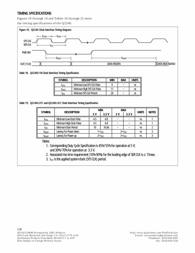
2-20QUALCOMM Incorporated, ASIC Products http://www.qualcomm.com/ProdTech/asic6455 Lusk Boulevard, San Diego, CA 92121-2779, USA E-mail: [email protected] Products Data Book, 80-24127-1 A, 8/97 Telephone: (619) 658-5005Data Subject to Change Without Notice Fax: (619) 658-1556
TIMING SPECIFICATIONSFigures 10 through 14 and Tables 18 through 25 show
the timing specifications of the Q2240.
Figure 10. Q2240 Clock Interface Timing Diagram
SYS CLKSER CLK
PWR DN/
OUT [13:0] DATA FROZEN DATA REACTIVATED
tCYC
tCYCH tCYCL
tPDLAT tPULAT
Table 18. Q2240I-1N Clock Interface Timing Specification
SYMBOL
tCYCL
tCYCH
tCYC
DESCRIPTION MIN
91120
MAX–––
UNITS
nsnsns
Minimum Low SYS CLK PulseMinimum High SYS CLK PulseMinimum SYS CLK Period
Table 19. Q2240I-2S1 and Q2240I-3S1 Clock Interface Timing Specification
SYMBOL
tCYCL
tCYCH
tCYC
tPDLAT
tPULAT
Notes:1. Corresponding Duty Cycle Specification is 45%/55% for operation at 5 V; and 30%/70% for operation at 3.3 V.2. Associated rise time requirement (10%-90%) for the leading edge of SER CLK is ≤ 15nsec.3. tCYC is the applied system clock (SYS CLK) period.
DESCRIPTION5 V
4.54.510
MIN
1* tCYC
2* tCYC
MAX
2* tCYC
3* tCYC
5 V–––
3.3 V
4.84.8
16.66
3.3 V–––
UNITS
nsnsnsnsns
NOTES
11233
Minimum Low Clock PulseMinimum High Clock PulseMinimum Clock PeriodLatency for Power-downLatency for Power-up
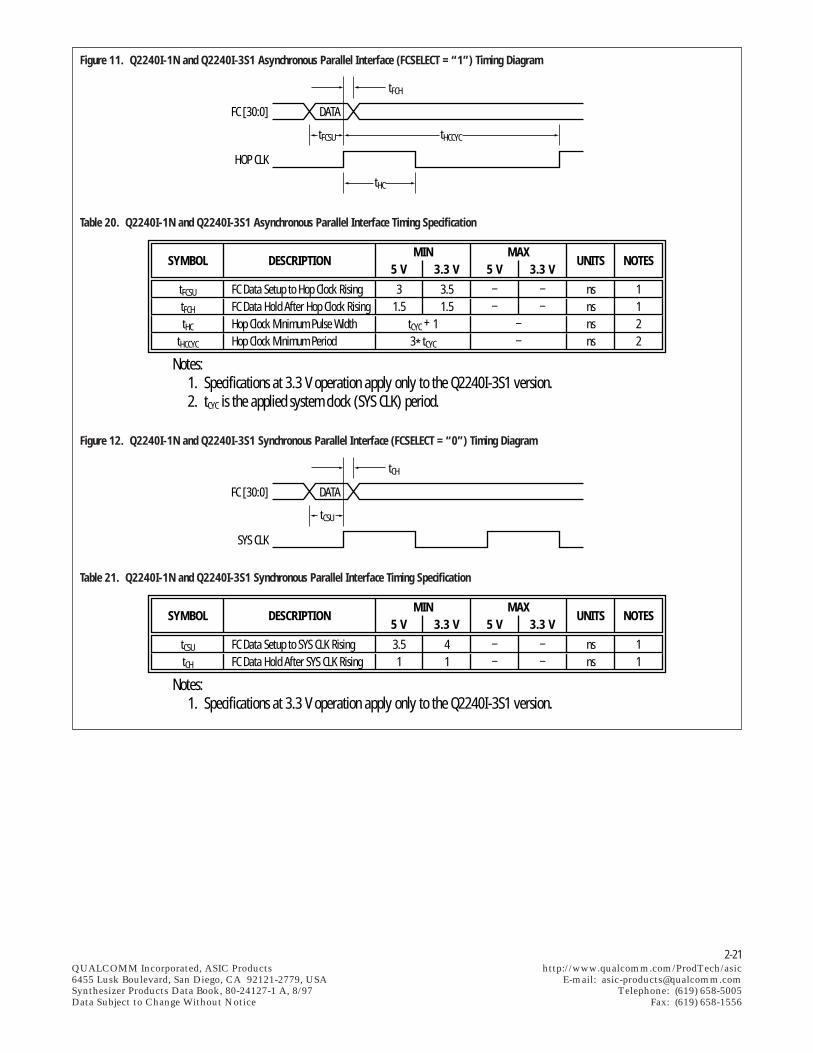
2-21QUALCOMM Incorporated, ASIC Products http://www.qualcomm.com/ProdTech/asic6455 Lusk Boulevard, San Diego, CA 92121-2779, USA E-mail: [email protected] Products Data Book, 80-24127-1 A, 8/97 Telephone: (619) 658-5005Data Subject to Change Without Notice Fax: (619) 658-1556
DATAFC [30:0]
HOP CLK
tFCH
tFCSU tHCCYC
tHC
Figure 11. Q2240I-1N and Q2240I-3S1 Asynchronous Parallel Interface (FCSELECT = “1”) Timing Diagram
Table 20. Q2240I-1N and Q2240I-3S1 Asynchronous Parallel Interface Timing Specification
SYMBOL
tFCSU
tFCH
tHC
tHCCYC
Notes:1. Specifications at 3.3 V operation apply only to the Q2240I-3S1 version.2. tCYC is the applied system clock (SYS CLK) period.
DESCRIPTION5 V
31.5
MIN
tCYC + 13* tCYC
MAX
––
5 V––
3.3 V
3.51.5
3.3 V––
UNITS
nsnsnsns
NOTES
1122
FC Data Setup to Hop Clock RisingFC Data Hold After Hop Clock RisingHop Clock Minimum Pulse WidthHop Clock Minimum Period
Figure 12. Q2240I-1N and Q2240I-3S1 Synchronous Parallel Interface (FCSELECT = “0”) Timing Diagram
DATAFC [30:0]
SYS CLK
tCH
tCSU
Table 21. Q2240I-1N and Q2240I-3S1 Synchronous Parallel Interface Timing Specification
SYMBOL
tCSU
tCH
Notes:1. Specifications at 3.3 V operation apply only to the Q2240I-3S1 version.
DESCRIPTION5 V
3.51
MIN MAX5 V––
3.3 V
41
3.3 V––
UNITS
nsns
NOTES
11
FC Data Setup to SYS CLK RisingFC Data Hold After SYS CLK Rising
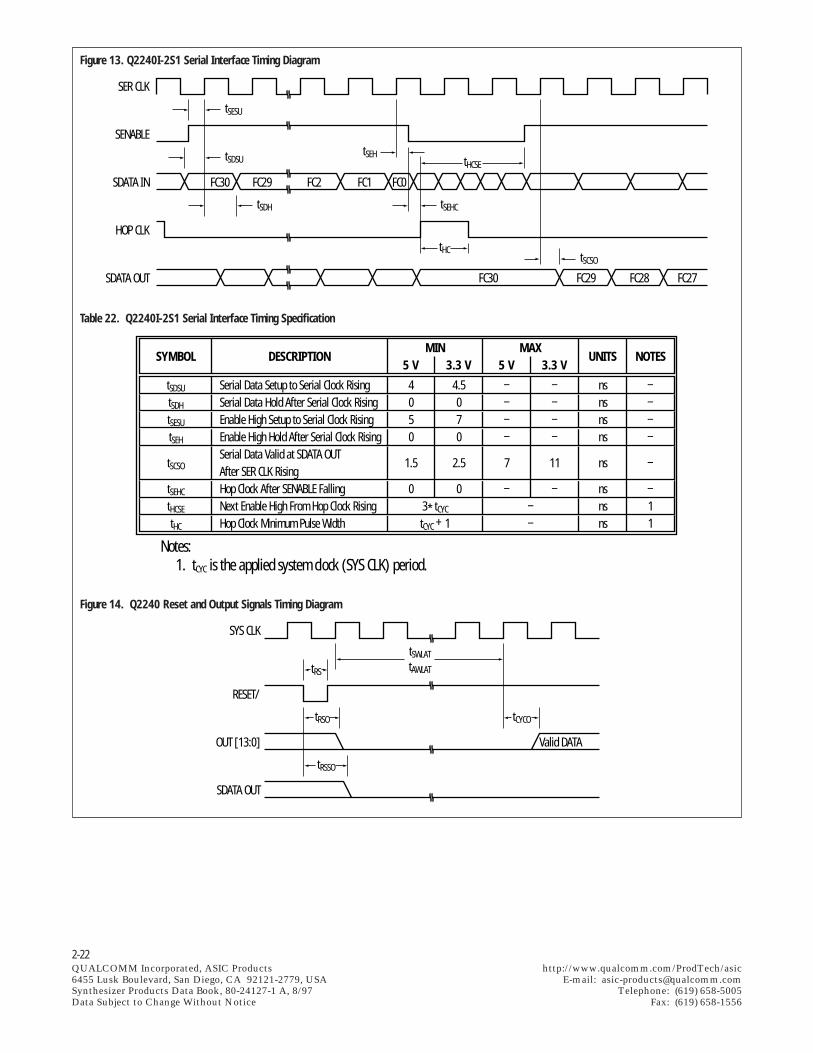
2-22QUALCOMM Incorporated, ASIC Products http://www.qualcomm.com/ProdTech/asic6455 Lusk Boulevard, San Diego, CA 92121-2779, USA E-mail: [email protected] Products Data Book, 80-24127-1 A, 8/97 Telephone: (619) 658-5005Data Subject to Change Without Notice Fax: (619) 658-1556
Figure 13. Q2240I-2S1 Serial Interface Timing Diagram
SER CLK
SENABLE
SDATA IN
HOP CLK
SDATA OUT
tSESU
tSDSU
tSDH tSEHC
tSCSO
tSEHtHCSE
tHC
FC30 FC29 FC2 FC1 FC0
FC30 FC29 FC28 FC27
Table 22. Q2240I-2S1 Serial Interface Timing Specification
SYMBOL
tSDSU
tSDH
tSESU
tSEH
tSCSO
tSEHC
tHCSE
tHC
Notes:1. tCYC is the applied system clock (SYS CLK) period.
DESCRIPTION5 V
4050
1.5
0
MIN
3* tCYC
tCYC + 1
MAX
––
5 V––––
7
–
3.3 V
4.5070
2.5
0
3.3 V––––
11
–
UNITS
nsnsnsns
ns
nsnsns
NOTES
––––
–
–11
Serial Data Setup to Serial Clock RisingSerial Data Hold After Serial Clock RisingEnable High Setup to Serial Clock RisingEnable High Hold After Serial Clock RisingSerial Data Valid at SDATA OUTAfter SER CLK RisingHop Clock After SENABLE FallingNext Enable High From Hop Clock RisingHop Clock Minimum Pulse Width
Figure 14. Q2240 Reset and Output Signals Timing Diagram
tRS
tSWLATtAWLAT
tRSO tCYCO
tRSSO
Valid DATA
SYS CLK
RESET/
OUT [13:0]
SDATA OUT
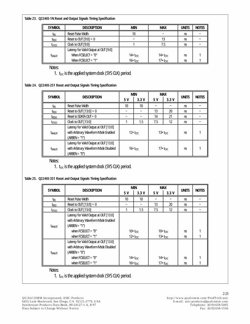
2-23QUALCOMM Incorporated, ASIC Products http://www.qualcomm.com/ProdTech/asic6455 Lusk Boulevard, San Diego, CA 92121-2779, USA E-mail: [email protected] Products Data Book, 80-24127-1 A, 8/97 Telephone: (619) 658-5005Data Subject to Change Without Notice Fax: (619) 658-1556
Table 23. Q2240I-1N Reset and Output Signals Timing Specification
SYMBOL
tRS
tRSO
tCYCO
tSWLAT
Notes:1. tCYC is the applied system clock (SYS CLK) period.
DESCRIPTION MIN
10–1
14* tCYC
16* tCYC
MAX–137.5
14* tCYC
17* tCYC
UNITS
nsnsns
nsns
NOTES––– 11
Reset Pulse WidthReset to OUT [9:0] = 0Clock to OUT [9:0]Latency for Valid Output at OUT [9:0] When FCSELECT = "0" When FCSELECT = "1"
Table 24. Q2240I-2S1 Reset and Output Signals Timing Specification
SYMBOL
tRS
tRSO
tRSSO
tCYCO
tAWLAT
tSWLAT
Notes:1. tCYC is the applied system clock (SYS CLK) period.
DESCRIPTION5 V
10––1
MIN
12* tCYC
16* tCYC
MAX
13* tCYC
17* tCYC
5 V–13147.5
3.3 V
10––
1.5
3.3 V–202112
UNITS
nsnsnsns
ns
ns
NOTES
––––
1
1
Reset Pulse WidthReset to OUT [13:0] = 0Reset to SDATA OUT = 0Clock to OUT [13:0]Latency for Valid Output at OUT [13:0]with Arbitrary Waveform Mode Enabled(ARBEN = "1")Latency for Valid Output at OUT [13:0]with Arbitrary Waveform Mode Disabled(ARBEN = "0")
Table 25. Q2240I-3S1 Reset and Output Signals Timing Specification
SYMBOL
tRS
tRSO
tCYCO
tAWLAT
tSWLAT
Notes:1. tCYC is the applied system clock (SYS CLK) period.
DESCRIPTION5 V
10–1
MIN
10* tCYC
12* tCYC
14* tCYC
16* tCYC
MAX
10* tCYC
13* tCYC
14* tCYC
17* tCYC
5 V–137.5
3.3 V
10–
1.5
3.3 V–2012
UNITS
nsnsns
nsns
nsns
NOTES
–––
11
11
Reset Pulse WidthReset to OUT [13:0] = 0Clock to OUT [13:0]Latency for Valid Output at OUT [13:0]with Arbitrary Waveform Mode Enabled(ARBEN = "1") when FCSELECT = "0" when FCSELECT = "1"Latency for Valid Output at OUT [13:0]with Arbitrary Waveform Mode Disabled(ARBEN = "0") when FCSELECT = "0" when FCSELECT = "1"
2-24QUALCOMM Incorporated, ASIC Products http://www.qualcomm.com/ProdTech/asic6455 Lusk Boulevard, San Diego, CA 92121-2779, USA E-mail: [email protected] Products Data Book, 80-24127-1 A, 8/97 Telephone: (619) 658-5005Data Subject to Change Without Notice Fax: (619) 658-1556
QUICK REFERENCE FOR Q2220I-50N TO Q2240I-1NMIGRATIONFCSELECT INPUTThe FCSELECT input (pin 3) is used to select
synchronous or asynchronous loading of the input
frequency value (FC0 - FC22) into the FC Register,
using either the system clock or HOP CLK signal,
respectively. When left floating, the FCSELECT on the
Q2220 would register as a logic “High” and therefore
automatically set the Q2220 for activation by the HOP
CLK signal. The Q2240I-1N does not have an internal
pull-up resistor on its FCSELECT input. Therefore, a
circuit that utilizes the device’s FCSELECT input while
left in a floating condition will have to connect a pull-
up resistor from pin 3 to VDD to ensure that the proper
logic state is set for this control. (Typical pull-up
resistor values are between 5 kΩ to 20 kΩ.)
RESET/ INPUTThe RESET/ input (pin 2) is used as an active “Low”
asynchronous clear function. When left floating, the
RESET/ on the Q2220 would register as a logic “High”
and therefore automatically set the Q2220 to not be in
a reset state. The Q2240I-1N does not have an internal
pull-up resistor on its RESET/ input. Therefore, a
circuit that utilizes the device’s RESET/ input while
left in a floating condition will have to connect a pull-
up resistor from pin 2 to VDD to ensure that the device
does not hang in a reset state. (Typical pull-up resistor
values are between 5 kΩ to 20 kΩ.)
NO CONNECT (N/C) PINSPins 19 and 20 for the Q2220 were specified as “No
Connect” and therefore no electrical connection should
be made to them. However, for the Q2240I-1N, pin 19
is tied internally to ground and pin 20 is tied internally
to VDD. These pins are still allowed to remain as “No
Connect” with no external electrical connection
without affecting the Q2240’s operation. However, as a
precaution, make sure that these pins are not
inadvertently tied to any electrical connection that
would affect the device.
POWERThe power consumption of the Q2240I-1N is rated at
(15mW/MHz) * (Clock Frequency) versus the Q2220
which has a lower rating of (5 mW/MHz) * (Clock
Frequency). This difference should be taken into
account for the overall current consumption burden of
the associated power supply, however, the Q2240I-1N
will not require any special thermal management to
sustain the rated operating junction temperature of less
than +150°C.
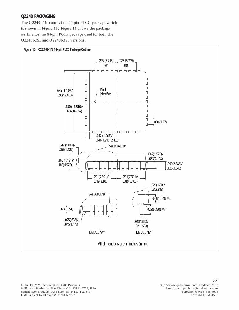
2-25QUALCOMM Incorporated, ASIC Products http://www.qualcomm.com/ProdTech/asic6455 Lusk Boulevard, San Diego, CA 92121-2779, USA E-mail: [email protected] Products Data Book, 80-24127-1 A, 8/97 Telephone: (619) 658-5005Data Subject to Change Without Notice Fax: (619) 658-1556
Q2240 PACKAGINGThe Q2240I-1N comes in a 44-pin PLCC package which
is shown in Figure 15. Figure 16 shows the package
outline for the 64-pin PQFP package used for both the
Q2240I-2S1 and Q2240I-3S1 versions.
Figure 15. Q2240I-1N 44-pin PLCC Package Outline
.225 (5.715)Ref.
.225 (5.715)Ref.
.685 (17.39)/.695(17.653)
.650 (16.510)/.656(16.662)
.291(7.391)/.319(8.103)
.062(1.575)/.083(2.108)
.013(.330)/.021(.533)
.025(.635)/
.045(1.143)
.026(.660)/
.032(.813)
.090(2.286)/
.120(3.048)
.291(7.391)/.319(8.103)
.042 (1.067)/
.048(1.219) 2PLCS.042 (1.067)/.056(1.422)
.165 (4.191)/
.180(4.572)
Pin 1Identifier
.050 (1.27)
See DETAIL "A"
See DETAIL "B"
DETAIL "A" DETAIL "B"
All dimensions are in inches (mm).
.045(1.143) Min.
.065(1.651) .025(6.350) Min.
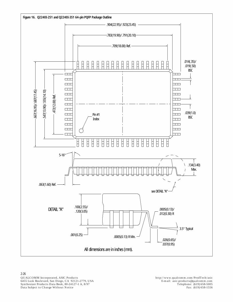
2-26QUALCOMM Incorporated, ASIC Products http://www.qualcomm.com/ProdTech/asic6455 Lusk Boulevard, San Diego, CA 92121-2779, USA E-mail: [email protected] Products Data Book, 80-24127-1 A, 8/97 Telephone: (619) 658-5005Data Subject to Change Without Notice Fax: (619) 658-1556
Figure 16. Q2240I-2S1 and Q2240I-3S1 64-pin PQFP Package Outline
.904(22.95)/.923(23.45)
.100(2.55)/.120(3.05)
.134(3.40)Max.
.783(19.90)/.791(20.10)
.709(18.00) Ref.
.667
(16.
95)/
.687
(17.
45)
.547
(13.
90)/
.555
(14.
10)
.472
(12.
00) R
ef.
Pin #1Index
.063(1.60) Ref.
.0005(0.13) R Min..001(0.25)
.0005(0.13)/
.012(0.30) R
.026(0.65)/
.037(0.95)
3.5° Typical
5-16°
see DETAIL "A"
.039(1.0)BSC
.014(.35)/.019(.50)
BSC
DETAIL "A"
All dimensions are in inches (mm).
2-27QUALCOMM Incorporated, ASIC Products http://www.qualcomm.com/ProdTech/asic6455 Lusk Boulevard, San Diego, CA 92121-2779, USA E-mail: [email protected] Products Data Book, 80-24127-1 A, 8/97 Telephone: (619) 658-5005Data Subject to Change Without Notice Fax: (619) 658-1556
EVALUATION SYSTEMS FOR THE Q2240 DDSsThe Q0340-2 and Q0340-3 DDS Evaluation Systems
were designed to demonstrate the capabilities and
operating modes of the Q2240I-2S1 and Q2240I-3S1,
respectively. The evaluation platform allows
customers to evaluate either the Q2240I-2S1 or Q2240I-
3S1 as a 5 V device operating at a maximum clock
frequency of 100 MHz or as a 3.3 V device operating at
a maximum clock frequency of 60 MHz. A block
diagram of the Q0340-2 and Q0340-3 DDS Evaluation
Systems are shown in Figure 17 and Figure 18. The
evaluation board contains the associated Q2240 device
coupled with a 100 MHz Digital-to-Analog Converter
and the necessary analog output circuitry to provide
optimum DDS performance. Both evaluation platforms
are computer controlled through a digital I/O board that
resides in the user’s personal computer and Windows™
based software.
Alternatively, the Q0340-3 can be controlled through
frequency control switches for stand-alone operation.
The Control Software will automatically compute all
desired frequency control words based upon the user’s
input and program the associated Q2240 DDS device.
The User’s Guide provides all information required to
operate the Q0340-2 or Q0340-3. Appendices are also
provided which contain the schematics, layout and
complete parts list.
The Q0340-2 and Q0340-3 consist of a DDS
Evaluation Board, Control Software, Control Cable,
Digital I/O (DIO) Board and DIO Board Installation
Software. In order to operate the DDS Evaluation
Board, the DIO Board needs to be installed in a PC. The
DIO Driver Software and the respective Control
Software need to be installed on the hard drive of the
PC. Both DDS Evaluation Systems require the
following computer hardware as a minimum to operate
in Remote Mode:
• PC 80386 or Better
• 4 MB RAM
• Math Co-processor
• Hard Drive
• Mouse
• Windows™ Version 3.1 or Windows ‘95™
• SVGA Video Card (1024 X 768 Resolution, Small
Fonts)
Note: Windows™ is a trademark of Microsoft®
Corporation.
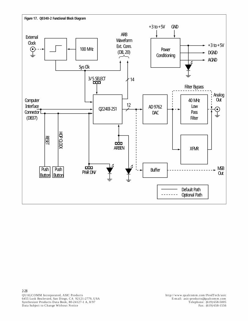
2-28QUALCOMM Incorporated, ASIC Products http://www.qualcomm.com/ProdTech/asic6455 Lusk Boulevard, San Diego, CA 92121-2779, USA E-mail: [email protected] Products Data Book, 80-24127-1 A, 8/97 Telephone: (619) 658-5005Data Subject to Change Without Notice Fax: (619) 658-1556
100 MHz
ARBWaveformExt. Conn.(DIL 20) Power
Conditioning
Q2240I-2S1 AD 9762DAC
40 MHzLowPassFilter
XFMR
PushButton
PushButton
ARBEN
PWR DN/
ComputerInterfaceConnector(DB37)
ExternalClock
RESET
HOP CLOCK
3/5 SELECT
Filter Bypass
AnalogOut
+3 to +5V
DGND
AGND
+3 to +5V GND
Default PathOptional Path
MSBOut
12
14
Sys Clk
Buffer
Figure 17. Q0340-2 Functional Block Diagram
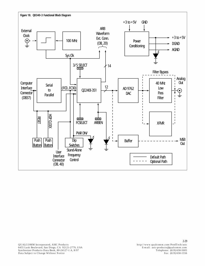
2-29QUALCOMM Incorporated, ASIC Products http://www.qualcomm.com/ProdTech/asic6455 Lusk Boulevard, San Diego, CA 92121-2779, USA E-mail: [email protected] Products Data Book, 80-24127-1 A, 8/97 Telephone: (619) 658-5005Data Subject to Change Without Notice Fax: (619) 658-1556
Figure 18. Q0340-3 Functional Block Diagram
100 MHz
ARBWaveformExt. Conn.(DIL 20) Power
Conditioning
Serialto
ParallelQ2240I-3S1 AD 9762
DAC
40 MHzLowPassFilter
XFMR
PushButton
PushButton
DipSwitches
Stand-AloneFrequency
Control
FCSELECT
PWR DN/
ARBEN
(FC0..FC30)ComputerInterfaceConnector(DB37)
ExternalClock
UserInterfaceConnector(DIL 40)
RESET
HOP CLOCK
3/5 SELECT
Filter Bypass
AnalogOut
+3 to +5V
DGND
AGND
+3 to +5V GND
Default PathOptional Path
MSBOut
12
14
Sys Clk
Buffer
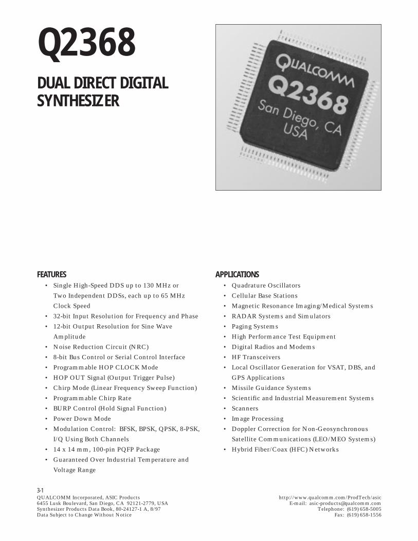
3-1QUALCOMM Incorporated, ASIC Products http://www.qualcomm.com/ProdTech/asic6455 Lusk Boulevard, San Diego, CA 92121-2779, USA E-mail: [email protected] Products Data Book, 80-24127-1 A, 8/97 Telephone: (619) 658-5005Data Subject to Change Without Notice Fax: (619) 658-1556
FEATURES• Single High-Speed DDS up to 130 MHz or
Two Independent DDSs, each up to 65 MHz
Clock Speed
• 32-bit Input Resolution for Frequency and Phase
• 12-bit Output Resolution for Sine Wave
Amplitude
• Noise Reduction Circuit (NRC)
• 8-bit Bus Control or Serial Control Interface
• Programmable HOP CLOCK Mode
• HOP OUT Signal (Output Trigger Pulse)
• Chirp Mode (Linear Frequency Sweep Function)
• Programmable Chirp Rate
• BURP Control (Hold Signal Function)
• Power Down Mode
• Modulation Control: BFSK, BPSK, QPSK, 8-PSK,
I/Q Using Both Channels
• 14 x 14 mm, 100-pin PQFP Package
• Guaranteed Over Industrial Temperature and
Voltage Range
APPLICATIONS• Quadrature Oscillators
• Cellular Base Stations
• Magnetic Resonance Imaging/Medical Systems
• RADAR Systems and Simulators
• Paging Systems
• High Performance Test Equipment
• Digital Radios and Modems
• HF Transceivers
• Local Oscillator Generation for VSAT, DBS, and
GPS Applications
• Missile Guidance Systems
• Scientific and Industrial Measurement Systems
• Scanners
• Image Processing
• Doppler Correction for Non-Geosynchronous
Satellite Communications (LEO/MEO Systems)
• Hybrid Fiber/Coax (HFC) Networks
Q2368DUAL DIRECT DIGITALSYNTHESIZER
3-2QUALCOMM Incorporated, ASIC Products http://www.qualcomm.com/ProdTech/asic6455 Lusk Boulevard, San Diego, CA 92121-2779, USA E-mail: [email protected] Products Data Book, 80-24127-1 A, 8/97 Telephone: (619) 658-5005Data Subject to Change Without Notice Fax: (619) 658-1556
CONTENTSQ2368 GENERAL DESCRIPTION ............................................................................................................................... 3-4
MODULATION TECHNIQUES .................................................................................................................................. 3-5
INTERNAL ARCHITECTURE ..................................................................................................................................... 3-5
Double Mode Operation ....................................................................................................................................... 3-5
Digital Processor Interface (DPI) Modes .............................................................................................................. 3-6
8-BIT Bus Mode ........................................................................................................................................... 3-6
Serial Bus Mode ........................................................................................................................................... 3-6
Phase Increment Registers (PIRs) ........................................................................................................................ 3-7
Mode Control Registers ....................................................................................................................................... 3-7
Synchronous Mode Control (SMC) Register .............................................................................................. 3-7
Asynchronous Mode Control (AMC) Register ........................................................................................... 3-9
Accumulator Reset Register (ARR) .......................................................................................................... 3-10
Asynchronous Hop Clock (AHC) ............................................................................................................. 3-11
Programmable Hop Clock (PHC) Register ............................................................................................... 3-11
HOP OUT Register .................................................................................................................................... 3-11
Programmable Chirp Rate (PCR) Register ............................................................................................... 3-11
Phase Increment Multiplexer Control .............................................................................................................. 3-12
Phase Accumulator ............................................................................................................................................ 3-12
Phase Modulation Control ................................................................................................................................. 3-12
Sine Lookup Function ........................................................................................................................................ 3-12
Noise Reduction Circuit (NRC) ........................................................................................................................ 3-12
INPUT/OUTPUT SIGNALS ....................................................................................................................................... 3-14
Signals Common for Both DDSs ....................................................................................................................... 3-16
Signals Independent for each DDS .................................................................................................................... 3-16
MODES OF OPERATION........................................................................................................................................... 3-19
Basic Synthesizer Mode ...................................................................................................................................... 3-19
Phase Modulation Mode .................................................................................................................................... 3-19
Internal Phase Modulation........................................................................................................................ 3-19
External Phase Modulation ....................................................................................................................... 3-20
Quadrature Signal Generation with the Q2368 ....................................................................................... 3-20
Binary Frequency Shift Keying (BFSK) Modulation Mode ................................................................................ 3-21
Minimum Shift Keying (MSK) Modulation Mode ............................................................................................ 3-21
Frequency Hopping Mode .................................................................................................................................. 3-21
Chirp Mode ......................................................................................................................................................... 3-22
3-3QUALCOMM Incorporated, ASIC Products http://www.qualcomm.com/ProdTech/asic6455 Lusk Boulevard, San Diego, CA 92121-2779, USA E-mail: [email protected] Products Data Book, 80-24127-1 A, 8/97 Telephone: (619) 658-5005Data Subject to Change Without Notice Fax: (619) 658-1556
Chirp Waveform Variations ...................................................................................................................... 3-22
Chirp Implementation .............................................................................................................................. 3-22
Programmable Chirp Rate (PCR) .............................................................................................................. 3-22
Piecewise Linear Chirp ............................................................................................................................. 3-22
Programmable Hop Clock (PHC) .............................................................................................................. 3-23
BURP Control ............................................................................................................................................ 3-23
Chirp Operations and Initialization ......................................................................................................... 3-23
Programming Operations for Chirp Mode ............................................................................................... 3-24
Limits on the Chirp Sequence Duration, t ............................................................................................... 3-25
Changing from a Chirp Waveform to a Non-Chirp Waveform ............................................................... 3-25
PIPELINE DELAY ........................................................................................................................................................ 3-26
TYPICAL EXAMPLES AND INITIAL SETUP OPERATIONS ................................................................................. 3-26
Simple Oscillator Mode ..................................................................................................................................... 3-27
Binary Frequency Shift Keying (BFSK) Mode .................................................................................................... 3-27
External Phase Modulation Mode ..................................................................................................................... 3-28
Frequency Hopping Mode .................................................................................................................................. 3-28
Internal Phase Modulation Mode ...................................................................................................................... 3-29
Chirp Mode ......................................................................................................................................................... 3-30
Example 1. Incrementing Chirp ............................................................................................................... 3-30
Example 2. Decrementing Chirp ............................................................................................................. 3-31
Example 3. Incrementing and Decrementing Chirp ............................................................................... 3-32
Example 4. Incrementing Chirp in Double Mode ................................................................................... 3-33
TECHNICAL SPECIFICATIONS ............................................................................................................................... 3-34
Absolute Maximum Ratings .............................................................................................................................. 3-34
DC Electrical Characteristics ............................................................................................................................ 3-35
Timing Specifications ........................................................................................................................................ 3-36
PQFP PACKAGING .................................................................................................................................................... 3-41
USING 3-WIRE EQUIVALENT SERIAL CONTROL FOR THE Q2368 .................................................................. 3-41
PATENT REFERENCES.............................................................................................................................................. 3-42
EVALUATION SYSTEM FOR THE Q2368 DDS ...................................................................................................... 3-42
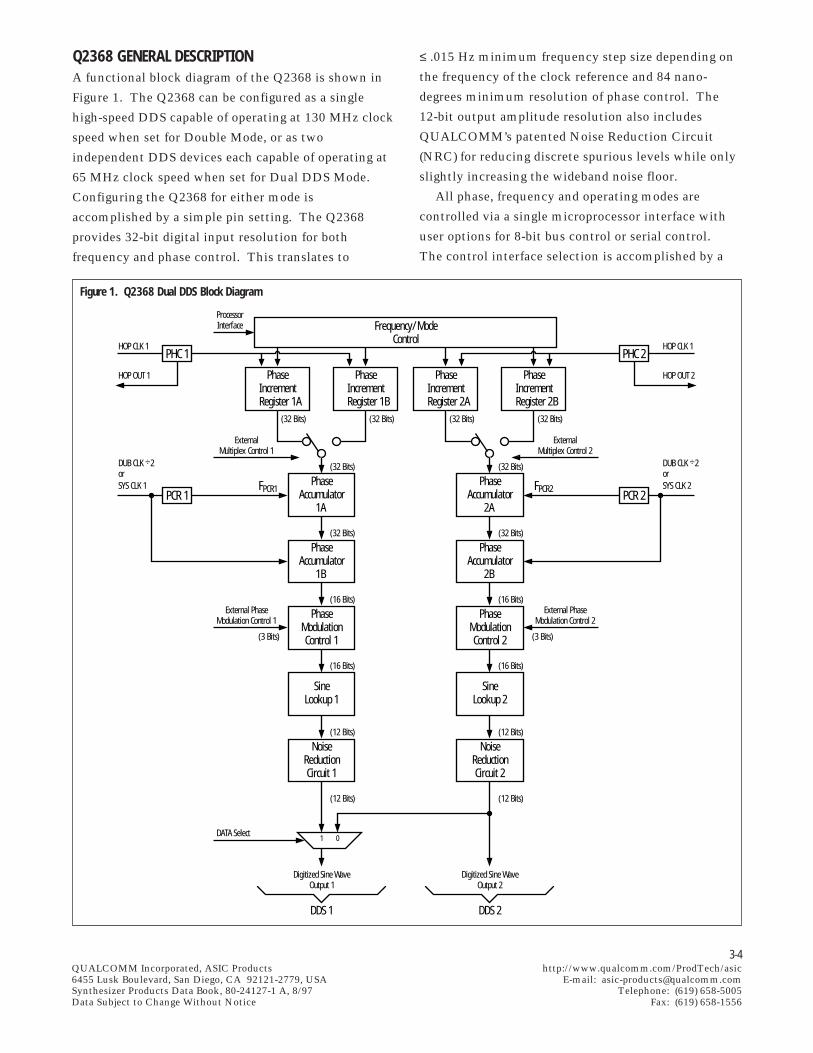
3-4QUALCOMM Incorporated, ASIC Products http://www.qualcomm.com/ProdTech/asic6455 Lusk Boulevard, San Diego, CA 92121-2779, USA E-mail: [email protected] Products Data Book, 80-24127-1 A, 8/97 Telephone: (619) 658-5005Data Subject to Change Without Notice Fax: (619) 658-1556
Q2368 GENERAL DESCRIPTIONA functional block diagram of the Q2368 is shown in
Figure 1. The Q2368 can be configured as a single
high-speed DDS capable of operating at 130 MHz clock
speed when set for Double Mode, or as two
independent DDS devices each capable of operating at
65 MHz clock speed when set for Dual DDS Mode.
Configuring the Q2368 for either mode is
accomplished by a simple pin setting. The Q2368
provides 32-bit digital input resolution for both
frequency and phase control. This translates to
≤ .015 Hz minimum frequency step size depending on
the frequency of the clock reference and 84 nano-
degrees minimum resolution of phase control. The
12-bit output amplitude resolution also includes
QUALCOMM’s patented Noise Reduction Circuit
(NRC) for reducing discrete spurious levels while only
slightly increasing the wideband noise floor.
All phase, frequency and operating modes are
controlled via a single microprocessor interface with
user options for 8-bit bus control or serial control.
The control interface selection is accomplished by a
Figure 1. Q2368 Dual DDS Block Diagram
ProcessorInterface
HOP CLK 1
HOP OUT 1
DUB CLK ÷2orSYS CLK 1
HOP CLK 1
HOP OUT 2
DUB CLK ÷2orSYS CLK 2
ExternalMultiplex Control 1
ExternalMultiplex Control 2
External PhaseModulation Control 2
External PhaseModulation Control 1
DATA Select
(32 Bits) (32 Bits) (32 Bits) (32 Bits)
(32 Bits)
(32 Bits)
(16 Bits)
(12 Bits)
(12 Bits)
(3 Bits) (3 Bits)
(32 Bits)
(32 Bits)
(16 Bits)
(12 Bits)
(12 Bits)
Digitized Sine WaveOutput 1
Digitized Sine WaveOutput 2
Frequency/ModeControl
PhaseIncrementRegister 1A
PhaseIncrementRegister 2A
PhaseIncrementRegister 2B
PhaseIncrementRegister 1B
PhaseAccumulator
1A
PhaseAccumulator
2A
(16 Bits) (16 Bits)
PhaseAccumulator
1B
PhaseAccumulator
2B
PhaseModulationControl 2
PhaseModulationControl 1
SineLookup 1
SineLookup 2
NoiseReductionCircuit 2
NoiseReductionCircuit 1
DDS 1 DDS 2
1 0
PHC 1
PCR 1
PHC 2
PCR 2FPCR1 FPCR2
3-5QUALCOMM Incorporated, ASIC Products http://www.qualcomm.com/ProdTech/asic6455 Lusk Boulevard, San Diego, CA 92121-2779, USA E-mail: [email protected] Products Data Book, 80-24127-1 A, 8/97 Telephone: (619) 658-5005Data Subject to Change Without Notice Fax: (619) 658-1556
simple pin setting. Serial data output is provided to
enable daisy-chaining of DDS1 to DDS2, or other
serial-controlled devices. User control of all functions
apply identically to either Double Mode or Dual Mode
operation.
The processor interface controls the phase and
frequency of the Q2368 DDS. The specific mode of
the DDS operation is controlled by the Synchronous
Mode Control (SMC) register and Asynchronous Mode
Control (AMC) register.
The AMC register has an active value once the
information has been written to it. This register does
not require a hop clock signal to become active.
The SMC register and the two PIRs are double
buffered. That is, these registers can be loaded at any
time using the processor interface, but the values
become active only when the hop clock signal is
asserted. This makes possible the advanced
synchronous phase and frequency change features of
the Q2368 which are especially important when using
the device in modulation or phase-locked loop
applications.
The Asynchronous Hop Clock (AHC) can also be
used to activate the double-buffered settings. See the
Asynchronous Hop Clock section.
MODULATION TECHNIQUESThe Q2368 DDS provides features which allow the
basic frequency synthesis function to be expanded and
used in a variety of phase and frequency modulation
schemes. Aside from the 32-bit control available for
frequency and/or phase manipulations using the
processor interface, external FSK and PSK modulation
inputs are also provided as convenient control ports.
The Q2368 can generate BFSK modulation up to 16.25
Mbps using the external multiplex control to toggle
between two pre-loaded frequencies. Using the 3-bit
external phase modulation control, either BPSK,
QPSK, or 8-PSK modulation can be generated up to
16.25 Mbps for continuous data transmission.
Additionally, when operating in Dual DDS Mode,
quadrature I and Q channels can be generated quite
simply by using the external phase control to produce
two signals which are 90° offset from one another.
INTERNAL ARCHITECTUREThe Q2368 includes two identical, independent DDS
functions with a common microprocessor interface
(see Figure 1). Each DDS includes two double-buffered
phase increment registers, two mode control registers
(SMC and AMC), a phase increment multiplexer, two
phase accumulators, a phase modulation control, a
sine lookup function, and a noise reduction function.
These components, and the processor interface, are
described in detail in the following sections.
DOUBLE MODE OPERATIONWhen operating in Double Mode, the Q2368 is
configured as one DDS capable of generating twice the
output frequency compared to DDS operation in Dual
Mode. The Double Mode is activated when the DUB
EN input is set to a logic “High”. Operating in Double
Mode requires a separate clock source input (DUB
CLK) to be used, rather than the system clock inputs
(SYS CLK1, SYS CLK2) used for Dual Mode, since it is
used for the multiplexing of both DDSs. Therefore,
the maximum rated clock speed for DUB CLK is
double that of the maximum rated clock speed for SYS
CLK1 and SYS CLK2 in Dual Mode operation
(130 MHz vs. 65 MHz).
The frequency output is directed through a mux to
become the digitized sine wave outputs of DDS1; these
are denoted separately as DUB OUT0 -11 and share the
same pins as the DAC1 BIT0 -11 outputs.
Internally, the DDS multiplexing involves
connecting the DUB CLK source to a 2-times mux for
interleaving DDS1 and DDS2 and then is divided-by
two and connected to each DDS for their associated
operation. However, Double Mode operation only
requires user control of DDS1 functions and modes of
operation to generate the desired output signal. That
is to say, all signal generation in Double Mode is
performed using the DDS1 interface, and accomplished
in an identical manner as with the controlling of DDS1
when operating in Dual Mode. The only exception to
this is the setting of the initialization commands and
activation of Power-down Mode.
During the initialization of the Q2368 operating in
Double Mode, the AMC register of both DDS1 and
3-6QUALCOMM Incorporated, ASIC Products http://www.qualcomm.com/ProdTech/asic6455 Lusk Boulevard, San Diego, CA 92121-2779, USA E-mail: [email protected] Products Data Book, 80-24127-1 A, 8/97 Telephone: (619) 658-5005Data Subject to Change Without Notice Fax: (619) 658-1556
Table 1. Q2368 Microprocessor Interface Register Address Map: 8-bit Parallel Loading
DDS1 REGISTERADDRESS (HEX)
000102030405060708090A0B0C0D0E0F14101112
DDS2 REGISTERADDRESS (HEX)
202122232425262728292A2B2C2D2E2F34303132
FUNCTION
PIRA Bits 0-7PIRA Bits 8-15PIRA Bits 16-23PIRA Bits 24-31PIRB Bits 0-7PIRB Bits 8-15PIRB Bits 16-23PIRB Bits 24-31SMCAMCARRAHCPHC Bits 0-7PHC Bits 8-15PHC Bits 16-23PHC Bits 24-31HOP OUT 0-3PCR Bits 0-7PCR Bits 8-15PCR Bits 16-19
DDS2 have to be loaded with identical values in order
to obtain the proper digitized output signals. Since the
Q2368 registers come up in a random state after supply
voltage is first applied, the initialization commands
must also include setting the SMC register of both
DDS1 and DDS2 in a known state such that the PWDE
bit is set to “0”. This will prevent the PWDE bit of
either SMC register from enabling an unwanted power-
down condition and interfering with Double Mode
operation. If activating the Power-down Mode is
desired, both SMC registers must have the PWDE bit
set to “1” in order to apply a complete power-down
condition. Alternatively, hardware control of power-
down requires both PWR DN/ signals to be set to a
logic “Low” and the respective DDS hop clock signals
asserted. The only other distinction between Double
Mode and Dual Mode operation is that in Double
Mode, all DDS operations are performed and
implemented with respect to the internal system clock
rate of DUB CLK/2. This means that all clock-related
calculations are performed in their usual method but
with respect to a system clock value of DUB CLK/2.
DIGITAL PROCESSOR INTERFACE (DPI) MODES8-BIT BUS MODEThe 8-bit Bus Mode interface is compatible with
commonly used 8-bit microprocessors. This mode is
selected when the BUSSELECT input (pin 51) is set
“Low”. The interface includes address decoding, chip
selection, and write controls to load all on-chip control
and phase increment registers in accordance with the
timing requirements shown in Figure 16 and Table 15.
Table 1 provides the register address map for the
device. Each register is write-only and is decoded from
the six-bit input address bus.
SERIAL BUS MODESerial Mode addressing is accomplished in a standard
fashion using four signals: SDATA IN, SER CLK,
SENABLE, and HOP CLK. With the BUSSELECT
input set “High”, the Serial Bus Mode is selected and
data is shifted serially into SDATA IN on the falling
edge of the SER CLK input while the shift enable
control input, SENABLE, is set “High”. The serial
programming register sequence for each DDS consists
of 144 bits. The data for all 144 programming bits is
shifted into the registers in accordance to the sequence
shown in Table 2, starting with the MSB of the PCR
register and ending with the LSB of the PIRA register.
Even though the PCR register has effectively 20 bits
and the HOP OUT register 4 bits, the serial update
must treat them as 24 bits and 8 bits, respectively. In
this case a logic “0” should be used for bits 1 through 4
Number of Bits
248
3288
3232
Register*
PCR (23...0)HOP OUT (7...0)
PHC (31... 0)AMC (7...0)SMC (7...0)
PIRB (31...0)PIRA (31...0)
* MSB is always input first, LSB input last.
Table 2. Q2368 Serial Programming Register Sequence
3-7QUALCOMM Incorporated, ASIC Products http://www.qualcomm.com/ProdTech/asic6455 Lusk Boulevard, San Diego, CA 92121-2779, USA E-mail: [email protected] Products Data Book, 80-24127-1 A, 8/97 Telephone: (619) 658-5005Data Subject to Change Without Notice Fax: (619) 658-1556
and 25 through 28. A serial data output, SDATA OUT,
is provided for each DDS to enable daisy-chaining of
DDS1 to DDS2, or other serial-controlled devices. The
serial data output timing is shown in Figure 17 and
Table 15. The SENABLE input must be held “High” for
the entire serial programming sequence and then set
“Low”. Letting SENABLE go “Low” before all of the
serial programming bits are loaded into the serial
registers will result in invalid programming to the
serial registers. The ARR and AHC registers are not
accessible in Serial Programming Mode. These
registers can only be accessed through their respective
external pins. After the SENABLE input is set “Low”,
the contents are activated on the rising edge of the
HOP CLK input according to the timing requirements
shown in Figure 17 and Table 16.
PHASE INCREMENT REGISTERS (PIRs)Two independent 32-bit phase increment registers
(A and B) are provided for each DDS function in the
Q2368. Each phase increment register is 32-bits wide.
Phase Increment Register A (PIRA) of each DDS
provides the phase increment for the most basic single-
frequency operation. Phase Increment Register B
(PIRB) provides the phase increment for a range of
functions useful in various modes of operation of the
DDS. The 32-bit value for each register is loaded using
four 8-bit write operations, or via serial programming.
As stated previously, each PIR is double-buffered and
the phase increment used by the phase accumulator is
unaffected by this new stored value until the assertion
of the hop clock signal occurs.
MODE CONTROL REGISTERSEach DDS function on the Q2368 includes two mode
control registers: Synchronous Mode Control (SMC)
register and Asynchronous Mode Control (AMC)
register. The SMC is used for operations that may
change throughout the operation of the DDS. The
AMC should be setup once during initialization.
(Please note that in Figures 2 and 3, the unused bits
must be set to “0” for proper operation.)
SYNCHRONOUS MODE CONTROL (SMC) REGISTERThe Synchronous Mode Control (SMC) register is
double buffered to update control information, which
will affect the actual DDS operation only when
synchronously enabled by the transition of the hop
clock signal. Figure 2 provides the bit definition for
this SMC register. Bit 5, and 7 are reserved and should
be set to logic “0”. The remaining bits of the SMC
register are the Power-down Enable (PWDE),
Programmable Hop Clock Enable (PHCE), Hop Clock
Phase Modulation Enable (HPME), External
Multiplexer Enable (EME), External Phase Modulation
Enable (EPME), and the Chirp Enable (CHE). Each of
these bits is described below.
POWER DOWN ENABLE (PWDE)
The Power-down Mode is armed by the PWDE bit.
This function provides independent power-down
control for each DDS when operating in Dual Mode, or
a combined power-down function while operating the
Q2368 as one DDS in Double Mode. The PWDE bit
allows processor control of power-down in an identical
0* 0*
HOP CLKPHASE MOD
ENABLE(HPME)
PROGHOP CLKENABLE(PHCE)
POWERDOWNENABLE(PWDE)
CHIRPENABLE(CHE)
D7 D6 D5 D4 D3 D2 D1 D0
EXTMUX
ENABLE(EME)
EXT PHASEMOD
ENABLE(EPME)
ADDRESS 08 or 28 [hex]* These bits must be set to 0.
Figure 2. Q2368 Synchronous Mode Control (SMC) Register
3-8QUALCOMM Incorporated, ASIC Products http://www.qualcomm.com/ProdTech/asic6455 Lusk Boulevard, San Diego, CA 92121-2779, USA E-mail: [email protected] Products Data Book, 80-24127-1 A, 8/97 Telephone: (619) 658-5005Data Subject to Change Without Notice Fax: (619) 658-1556
fashion as with the assertion of the PWR DN/ signal to
a logic “Low”. When the PWDE bit is set to “1”, the
power-down function is armed. The next time the hop
clock signal is asserted, DDS current consumption is
reduced to within the 0.1 to 20 mA range, depending
on the clock frequency and whether the device is
operating in Dual Mode or Double Mode. (See Table 3
for current consumption with different operating
conditions.) When the Q2368 is operating in Double
Mode, both DDS register addresses will have to be set
to “1” in order to apply a complete power-down
condition. All data residing in the programming
registers is retained during power-down, although new
information can still be addressed via the processor
interface. Since the Q2368 registers come up in a
random state after supply voltage is first applied, the
initialization of the DDS must also include setting the
SMC register in a known state such that the PWDE bit
is set to “0”. This will prevent the PWDE bit from
enabling an unwanted power-down condition and
interfering with normal DDS operation.
signal is asserted, the PHC register is activated. This
is used by the Q2368 as a built-in timer function
which allows precision timed intervals of the hop
clock command to be automatically and continuously
reasserted at the pre-programmed intervals of TPHC .
The sequence continues repetitively once it is started
until the Programmable Hop Clock Mode is disabled.
This significantly eases the control burden and
“housekeeping” from the microprocessor required for
programmable routines and sequential modes of
operation.
HOP CLOCK PHASE MODULATION ENABLE (HPME)
The HPME bit is used when operating in the Internal
Phase Modulation Mode and Chirp Mode. When the
HPME bit is set to logic “1”, the phase increment
value stored in PIRB is added to the phase accumulator
once each time the hop clock signal is asserted. In the
case of using the Internal Phase Modulation Mode
with the Phase Modulation Add Enable (PMAE) bit set
to logic “0”, all 32 bits of PIRB are used for the one
time. However, if the PMAE bit is set to “1”, the
8 MSB of PIRB are added to the 8 MSB of PIRA to form
the 8 MSB to be accumulated with the 24 LSB of PIRA.
The Chirp Mode and the Internal Phase Modulation
Mode utilize the HPME bit. When the HPME bit is set
to “1”, the hop clock signal is internally extended to
two system clock cycles. The two system clock cycles
make it possible for Phase Accumulator A to add the
contents from PIRB once, and then switch the process
immediately back to PIRA.
It is necessary to reset the HPME to “0” when you
want to stop Chirp Mode, or disable the Internal Phase
Modulation Mode and reconfigure operation to the
Basic Oscillator Mode, for example. The hop clock
command is required to initiate this change and during
the HPME’s transition from “1” to “0”, the hop clock
signal is correspondingly extended to two system clock
cycles. This results in an automatic switch of the
accumulation process back to PIRA.
EXTERNAL MULTIPLEXER ENABLE (EME)
The EME bit enables the External Multiplex Control.
When this bit is set to logic “1”, the EXT MUX signal
Operating ConditionsCurrent Consumption (mA)
Power-up Active Power-down Active
Dual Mode*, FCLK = 20 MHzDual Mode*, FCLK = 35 MHzDual Mode*, FCLK = 50 MHzDual Mode*, FCLK = 65 MHzDouble Mode, FCLK = 80 MHzDouble Mode, FCLK = 100 MHzDouble Mode, FCLK = 115 MHzDouble Mode, FCLK = 130 MHz
*Includes both DDSs (DDS1 and DDS2) operating concurrently.
60105150200125150180205
0.51.02.02.011.013.015.016.0
PROGRAMMABLE HOP CLOCK ENABLE (PHCE)
The Programmable Hop Clock Mode is armed when
the PHCE bit is set to “1”. This mode activates a
programmable 32-bit duration counter (PHC register)
derived from the DDS system clock to produce the
PHC time period, TPHC . The PHCE bit allows
processor control of the programmable hop clock in an
identical fashion as with the assertion of the PHOPEN
signal to a logic “High”. The next time the hop clock
Table 3. Q2368 Typical Current Consumption at Different Operating Conditions
3-9QUALCOMM Incorporated, ASIC Products http://www.qualcomm.com/ProdTech/asic6455 Lusk Boulevard, San Diego, CA 92121-2779, USA E-mail: [email protected] Products Data Book, 80-24127-1 A, 8/97 Telephone: (619) 658-5005Data Subject to Change Without Notice Fax: (619) 658-1556
determines whether the value stored in PIRA or PIRB
will be used for the phase accumulation process. The
selection on the EXT MUX signal is synchronously
activated on the rising edge of the MUX CLK signal
when the EME is set to logic “1”. If the EME bit is set
to logic “0”, then the External Multiplex Control is
disabled and the signal on EXT MUX is ignored. In
this case, the contents of PIRA will be used for the
accumulation process.
EXTERNAL PHASE MODULATION ENABLE (EPME)
The EPME enables the External Phase Modulation
function. When this bit is set to “1”, the PM EXT
BITS are read and the corresponding phase offset is
latched into the Q2368 each time the PM CLK is
asserted. If External Phase Modulation is not used, set
the EPME bit to “0”. (See the External Phase
Modulation section.)
CHIRP ENABLE (CHE)
The Chirp Mode is armed when the CHE bit is set to
“1”. To initiate a chirp waveform, both the HPME bit
and the CHE bit in the SMC register must be set to
“1”, however the CHE bit is used for chirp waveform
generation only and should be disabled whenever a
non-chirp waveform is desired. (See Chirp Mode
section under Modes of Operation.)
ASYNCHRONOUS MODE CONTROL (AMC) REGISTERThe Asynchronous Mode Control (AMC) register of
each DDS function includes control bits which should
only be configured during initialization of the Q2368.
During the initialization of the Q2368 operating in
Double Mode, the AMC register of both DDS1 and
DDS2 have to be loaded with identical values in order
to obtain the proper digitized output signals. These
control bits, as shown in Figure 3, include the DAC
Strobe or DAC Strobe Invert (DACSTB, DACSTB/),
Phase Modulation Add Enable (PMAE), Output
Format, and NRC Enable. Each of these is described
below. Bits 4 and 5 of the AMC register are reserved
and should be set to “0”.
DAC STROBE, DAC STROBE INVERT (DACSTB, DACSTB/)
The DAC Strobe is a delayed version of the system
clock which is provided along with the DAC BIT
outputs in order to facilitate strobing this digitized
sine value into a sample-and-hold DAC or other
Figure 3. Q2368 Asynchronous Mode Control (AMC) Register
DAC STB 0* 0* OUTPUTFORMAT**
D7 D6 D5 D4 D3 D2 D1 D0
PHASE MODADD
ENABLE(PMAE)
ADDRESS 09 or 29 [hex]
* These bits must be set to 0.
NRC ENABLE BITS***
***DAC SIZE(# OF BITS)
6789
101112
DISABLE NRC
D2
00001111
D1
00110011
D0
01010101
**Output FormatTwo's Complement
Offset Binary
D301
3-10QUALCOMM Incorporated, ASIC Products http://www.qualcomm.com/ProdTech/asic6455 Lusk Boulevard, San Diego, CA 92121-2779, USA E-mail: [email protected] Products Data Book, 80-24127-1 A, 8/97 Telephone: (619) 658-5005Data Subject to Change Without Notice Fax: (619) 658-1556
overhead required to control the DDS function in
rapidly switching phase modulation systems. When
the PMAE bit is set to logic “0”, all 32-bits of PIRB
will be accumulated in the phase accumulator when
PIRB is active allowing a phase resolution of 360°/232,
i.e, 84 nano-degrees.
OUTPUT FORMAT
The Output Format bit determines the binary coding
of the DAC output bits of each DDS function. When
this bit is set to logic “1”, the DAC output is encoded
in offset binary format. When this bit is set to logic
“0”, the DAC output bits are encoded in two’s
complement format. Table 4 shows the effect of the
setting of the Output Format bit.
VALUE
MAX Value………
Half MAX + 1Half MAX – 1
………
MIN Value
OUTPUT FORMAT = 1(OFFSET BINARY)
1 1 1 1 1 1 1 1 1 1 1 11 1 1 1 1 1 1 1 1 1 1 0
……
1 0 0 0 0 0 0 0 0 0 0 00 1 1 1 1 1 1 1 1 1 1 1
……
0 0 0 0 0 0 0 0 0 0 0 10 0 0 0 0 0 0 0 0 0 0 0
OUTPUT FORMAT = 0(TWO's COMPLEMENT)
0 1 1 1 1 1 1 1 1 1 1 10 1 1 1 1 1 1 1 1 1 1 0
……
0 0 0 0 0 0 0 0 0 0 0 01 1 1 1 1 1 1 1 1 1 1 1
……
1 0 0 0 0 0 0 0 0 0 0 11 0 0 0 0 0 0 0 0 0 0 0
LSBMSB LSBMSB
register. A non-inverted or inverted DAC Strobe is
provided so that DAC devices with different triggering
requirements can be easily accommodated. The DAC
Output Timing specifications must be synchronized
with respect to the falling edge of SYS CLK (or DUB
CLK) and are therefore only guaranteed in relation to
the falling edge of SYS CLK (or DUB CLK). Trying to
use the DACSTB timing associated with the rising edge
of SYS CLK (or DUB CLK) could potentially violate
DAC setup time and result in strobing erroneous DAC
BIT data.
When the AMC’s D7 register is set to a “0”, the
DAC Strobe is non-inverted in relation to the system
clock. This allows the falling edge of DACSTB to be
used in compliance with SYS CLK (or DUB CLK).
When the D7 register is set to a “1”, the sense of the
DAC Strobe is inverted in relation to the system clock.
This allows the rising edge of DACSTB to be used in
compliance with SYS CLK (or DUB CLK).
PHASE MODULATION ADD ENABLE (PMAE)
The PMAE bit is not used unless the HPME bit is set to
“1” when operating in the Internal Phase Modulation
Mode. The PMAE bit controls the way in which the
value stored in PIRB is used for the one-time
accumulation by the phase accumulator. When the
PMAE bit is set to logic “1” and PIRB is active for
accumulation, the 8 MSB of PIRB are added to the
8 MSB of PIRA to form the 8 MSB to be accumulated.
The 24 LSB of PIRA are used as the 24 LSB of the phase
accumulator input value. This technique allows
efficient control for systems utilizing the Internal Phase
Modulation Mode of operation. By storing the
synthesizer frequency in the PIRA and modifying only
the most significant byte of the PIRB, a 256-state phase
modulator is implemented. This feature saves
computation time in the processor controlling the DDS
operation when a phase modulation system with
256-state (i.e., 360°/256 = 1.41 degrees) phase resolution
is adequate. Using only the 8 MSB of PIRB to control
the phase modulation allows the user to establish a
byte-wide Direct Memory Access (DMA) control from
the processor to the DDS function phase modulation
register (i.e., PIRB), thus simplifying the processor
Table 4. Q2368 DAC Output Formats
NRC ENABLE
When using the on-chip Noise Reduction Circuit
(NRC) function, the number of significant bits to be
used from the DAC outputs must be programmed into
NRC Enable bits. The DAC bit-width is encoded in
three bits as shown in Figure 3. When using a DAC
with fewer than 12-bits resolution, the most
significant DAC output bits are valid. The NRC
function is disabled when the NRC Enable bits are set
to 111 (binary). The function of the NRC circuit is
described in the Noise Reduction Circuit section.
ACCUMULATOR RESET REGISTER (ARR)Each DDS function on the Q2368 device includes an
3-11QUALCOMM Incorporated, ASIC Products http://www.qualcomm.com/ProdTech/asic6455 Lusk Boulevard, San Diego, CA 92121-2779, USA E-mail: [email protected] Products Data Book, 80-24127-1 A, 8/97 Telephone: (619) 658-5005Data Subject to Change Without Notice Fax: (619) 658-1556
accumulator reset register (ARR) and an external
accumulator reset which is applied to the ARE/ input
pin. By writing any value to the ARR register or by
setting the ARE/ input to a logic “Low”, the
accumulator reset function is armed. The next time
the hop clock signal is asserted, all activated phase
accumulators are reset to zero.
ASYNCHRONOUS HOP CLOCK (AHC)Each DDS function includes an Asynchronous Hop
Clock (AHC) register. When any value is written to
this register, the previously stored values in the
double-buffered PIRA, PIRB, and SMC registers are
activated. This allows processor control of activation
of these settings in an identical fashion as with the
assertion of the HOP CLK signal. Note that the HOP
CLK signal must be low when the AHC register is
accessed in order to activate the new register values.
Also note that the timing for the AHC is exactly the
same as the HOP CLK signal. Activation of the stored
settings occurs within four SYS CLK or eight DUB
CLK periods after writing to the AHC register.
PROGRAMMABLE HOP CLOCK (PHC) REGISTERA desired duration, τ , over which a given DDS
operation is directed, can be controlled very precisely
using the Programmable Hop Clock Mode. This mode
introduces a programmable counter derived from the
DDS clock reference. The Programmable Hop Clock
Mode gets armed using either the PHOPEN input pin
or the PHCE bit in the SMC register. In conjunction
with this, the 32-bit PHC register is loaded with the
corresponding value to count the number of system
clock periods before another hop clock command gets
automatically issued and activates the latest
instruction routine programmed to follow. The PHC
register value corresponding to the desired duration for
a given programmable hop clock period is determined
as follows:
PHC = [(τ/TCLK) -1],
where TCLK = 1/FCLK, and τ = TPHC = the desired
PHC time period. (Please refer to Modes of
Operation in the Chirp Mode section.)
HOP OUT REGISTERWhile operating in the Programmable Hop Clock
Mode, an output pulse is generated at the HOP OUT
pin when the programmable hop clock resets itself
according to its programmed time interval, TPHC . The
4-bit HOP OUT register is included to adjust the HOP
OUT output pulse up to ± 7 system clock cycles of
delay to compensate for any circuit path delay
matching. The programming for this ± 7 clock cycles
adjustment is done using the sign magnitude format, as
shown in Table 5.
Table 5. Q2368 Programming for HOP OUT Register
HOP OUT RegisterProgramming
MSB LSB
011101100101010000110010000100001001101010111100110111101111
Adjustable Delay in# of System Clock
Cycles (tCYC)*+7+6+5+4+3+2+10-1-2-3-4-5-6-7
* When operating in Dual Mode, tCYC = the equivalent number of SYS CLK cycles. When operating in Double Mode, multiply tCYC by 2.
PROGRAMMABLE CHIRP RATE (PCR) REGISTERWhile operating in the Chirp Mode, the chirp rate
control introduces a programmable counter derived
from the DDS clock reference. The 20-bit PCR register
divides down the DDS system clock, FCLK , to produce
the chirp rate clock, FPCR, for Phase Accumulator A
used in the chirp implementation. If a new PCR value
is programmed and then activated by a hop clock
during a Chirp Mode sequence, the chirp rate clock
will not change to the new FPCR rate until after the
3-12QUALCOMM Incorporated, ASIC Products http://www.qualcomm.com/ProdTech/asic6455 Lusk Boulevard, San Diego, CA 92121-2779, USA E-mail: [email protected] Products Data Book, 80-24127-1 A, 8/97 Telephone: (619) 658-5005Data Subject to Change Without Notice Fax: (619) 658-1556
PCR register has completed its divide count down to
the current FPCR clock cycle and then it will reset to
start its new FPCR divide cycle. In conjunction with
the increment value in PIRA , the chirp rate control is
used by the Q2368 to achieve < 1Hz/sec minimum
chirp sweep rate over the entire clock speed range.
The PCR register value corresponding to the chirp rate
clock for a desired chirp sweep rate is determined as
follows:
PCR = (FCLK /∆FPCR ) - 1
where ∆FPCR is the desired switching speed.
(Additional reference is found under Modes of
Operation in the Chirp Mode section.)
PHASE INCREMENT MULTIPLEXER CONTROLThe Phase Increment Multiplexer function selects
which PIR (A or B) is used for the accumulation
process. This multiplexing function provides a simple
Binary Frequency Shift Keying (BFSK) interface to the
DDS. The signal EXT MUX controls the selection of
the value stored in either PIRA or PIRB. For
EXT MUX = 0, PIRA is selected; for EXT MUX = 1,
PIRB is selected. The signal MUX CLK enables the
selection made by the EXT MUX signal. The selection
made by the EXT MUX signal is activated
synchronously once during the low-to-high transition
on the MUX CLK signal. The MUX CLK signal is
internally synchronized to the system clock signal of
the DDS. The selection of the EXT MUX control may
occur as frequently as once every four periods of SYS
CLK or every eight periods of DUB CLK. (Refer to the
External Control Timing section.)
PHASE ACCUMULATORTwo 32-bit wide phase accumulators, cascaded serially,
are included in each DDS of the Q2368. The first
accumulator (Phase Accumulator A) is used for all
signal generation including chirp waveforms. The
second accumulator (Phase Accumulator B) is enabled
exclusively for chirp waveform generation in
conjunction with the first accumulator when Chirp
Mode operation is activated. These accumulators
compute and store the sum of the previously computed
phase value and the phase increment value from either
PIRA or PIRB.
PHASE MODULATION CONTROLUsing the external phase modulation inputs, PM EXT
BIT0-2, the output of the phase accumulator can be
offset by phase increments of 45 degrees (from 0
degrees to 315 degrees) without affecting the operation
of the phase accumulator. Table 6 shows the phase
offset for the possible settings of the 3-bit external
phase modulation inputs. These inputs are latched
into the DDS function when the signal PM CLK is
asserted. Changes in the external phase modulation
are synchronized internally to the DDS function. This
provides a simple 8-Phase Shift Keying (8PSK)
interface to the DDS.
Refer to the Modes of Operation section for more
detailed information on phase modulation.
Table 6. Q2368 External Phase Modulation Offset Settings
000001111
PM EXT BIT100110011
201010101
ABSOLUTE PHASEOFFSET (degrees)
04590135180225270315
SINE LOOKUP FUNCTIONThe Q2368 DDS implements a patented technique to
generate a sine wave lookup (see Patent Reference 1).
This algorithm takes the 16 MSB from the phase
accumulator to generate a 12-bit sine wave value.
Using this high precision lookup function, the phase
truncation noise of the sine wave output is kept below
84 dB. This technique differs considerably from the
traditional method of using a ROM lookup function.
This advanced look-up technique provides highly
accurate and precise sine wave generation.
NOISE REDUCTION CIRCUIT (NRC)Noise due to amplitude quantization is often assumed
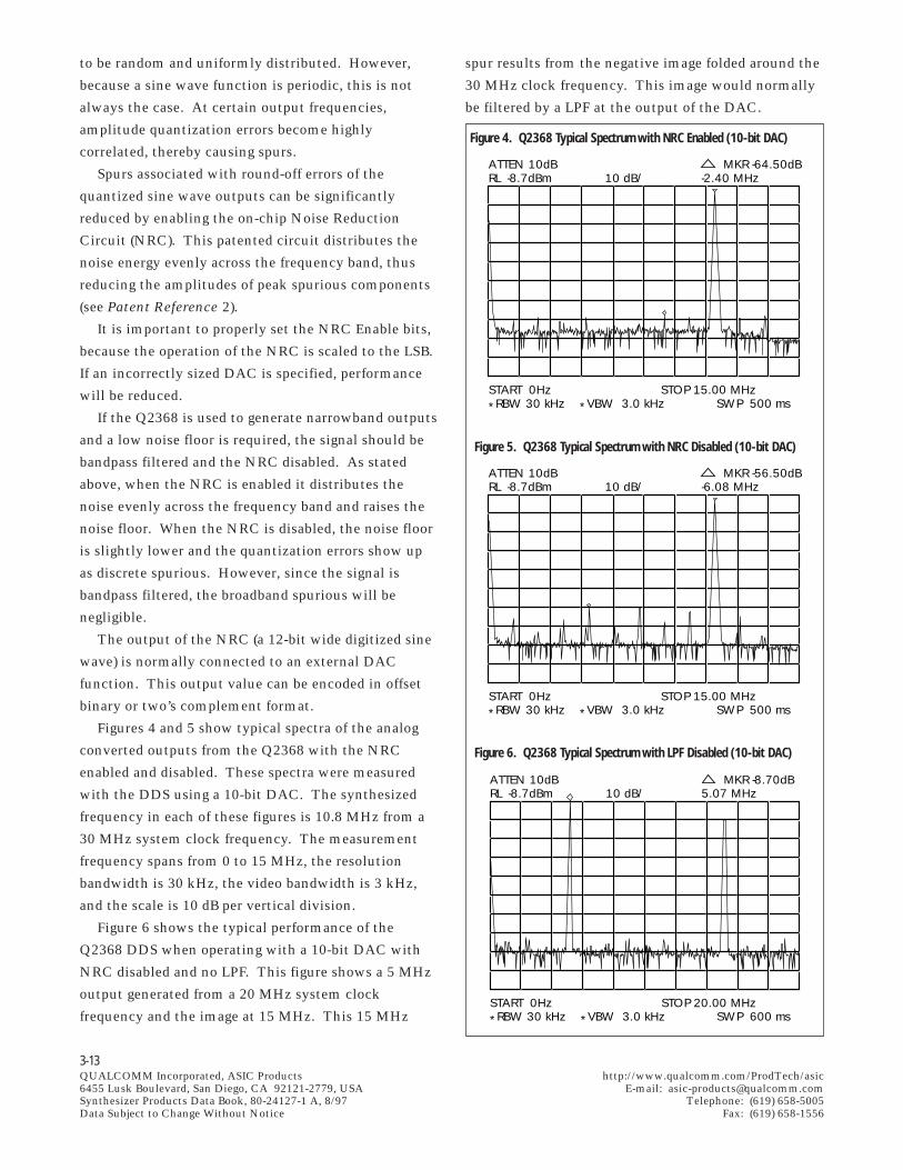
3-13QUALCOMM Incorporated, ASIC Products http://www.qualcomm.com/ProdTech/asic6455 Lusk Boulevard, San Diego, CA 92121-2779, USA E-mail: [email protected] Products Data Book, 80-24127-1 A, 8/97 Telephone: (619) 658-5005Data Subject to Change Without Notice Fax: (619) 658-1556
to be random and uniformly distributed. However,
because a sine wave function is periodic, this is not
always the case. At certain output frequencies,
amplitude quantization errors become highly
correlated, thereby causing spurs.
Spurs associated with round-off errors of the
quantized sine wave outputs can be significantly
reduced by enabling the on-chip Noise Reduction
Circuit (NRC). This patented circuit distributes the
noise energy evenly across the frequency band, thus
reducing the amplitudes of peak spurious components
(see Patent Reference 2).
It is important to properly set the NRC Enable bits,
because the operation of the NRC is scaled to the LSB.
If an incorrectly sized DAC is specified, performance
will be reduced.
If the Q2368 is used to generate narrowband outputs
and a low noise floor is required, the signal should be
bandpass filtered and the NRC disabled. As stated
above, when the NRC is enabled it distributes the
noise evenly across the frequency band and raises the
noise floor. When the NRC is disabled, the noise floor
is slightly lower and the quantization errors show up
as discrete spurious. However, since the signal is
bandpass filtered, the broadband spurious will be
negligible.
The output of the NRC (a 12-bit wide digitized sine
wave) is normally connected to an external DAC
function. This output value can be encoded in offset
binary or two’s complement format.
Figures 4 and 5 show typical spectra of the analog
converted outputs from the Q2368 with the NRC
enabled and disabled. These spectra were measured
with the DDS using a 10-bit DAC. The synthesized
frequency in each of these figures is 10.8 MHz from a
30 MHz system clock frequency. The measurement
frequency spans from 0 to 15 MHz, the resolution
bandwidth is 30 kHz, the video bandwidth is 3 kHz,
and the scale is 10 dB per vertical division.
Figure 6 shows the typical performance of the
Q2368 DDS when operating with a 10-bit DAC with
NRC disabled and no LPF. This figure shows a 5 MHz
output generated from a 20 MHz system clock
frequency and the image at 15 MHz. This 15 MHz
spur results from the negative image folded around the
30 MHz clock frequency. This image would normally
be filtered by a LPF at the output of the DAC.
ATTEN 10dBRL -8.7dBm 10 dB/
MKR -64.50dB-2.40 MHz
START 0Hz*RBW 30 kHz *VBW 3.0 kHz
STOP 15.00 MHzSWP 500 ms
ATTEN 10dBRL -8.7dBm 10 dB/
MKR -56.50dB-6.08 MHz
START 0Hz*RBW 30 kHz *VBW 3.0 kHz
STOP 15.00 MHzSWP 500 ms
Figure 4. Q2368 Typical Spectrum with NRC Enabled (10-bit DAC)
ATTEN 10dBRL -8.7dBm 10 dB/
MKR -8.70dB5.07 MHz
START 0Hz*RBW 30 kHz *VBW 3.0 kHz
STOP 20.00 MHzSWP 600 ms
Figure 5. Q2368 Typical Spectrum with NRC Disabled (10-bit DAC)
Figure 6. Q2368 Typical Spectrum with LPF Disabled (10-bit DAC)
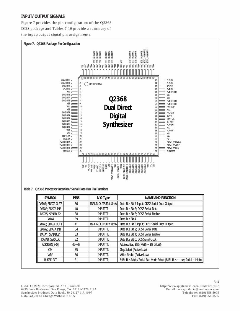
3-14QUALCOMM Incorporated, ASIC Products http://www.qualcomm.com/ProdTech/asic6455 Lusk Boulevard, San Diego, CA 92121-2779, USA E-mail: [email protected] Products Data Book, 80-24127-1 A, 8/97 Telephone: (619) 658-5005Data Subject to Change Without Notice Fax: (619) 658-1556
INPUT/OUTPUT SIGNALSFigure 7 provides the pin configuration of the Q2368
DDS package and Tables 7-10 provide a summary of
the input/output signal pin assignments.
Figure 7. Q2368 Package Pin Configuration
DAC2 BIT11DAC2 BIT10
DAC2 BIT9DAC2 STB
VDDDAC2 BIT8DAC2 BIT7DAC2 BIT6
VSSVDDVSS
DAC2 BIT5DAC2 BIT4DAC2 BIT3DAC2 BIT2DAC2 BIT1DAC2 BIT0
VDDVSS
HOP OUT2SYS CLK2
PM2 EXT BIT2PM2 EXT BIT1PM2 EXT BIT0
PM2 CLK
1 2 3 4 5 6 7 8 9 10111213141516171819202122232425
VDD
VSS
PHOP
EN2
PWR
DN2/
ARE2
/EX
T MUX
2 MU
X2 CL
KHO
P CL
K2BU
RP2
VSS
DATA
7 ; S
DATA
OUT
2VD
DDA
TA5
; SEN
ABLE
2DA
TA4
DATA
6 ; S
DATA
IN 2
DATA
3 ; S
DATA
OUT
1AD
DRES
S[5]
ADDR
ESS[
4]AD
DRES
S[3]
ADDR
ESS[
2]AD
DRES
S[1]
ADDR
ESS[
0]VD
DN/
CVS
S
26 27 28 29 30 31 32 33 34 35 36 37 38 39 40 41 42 43 44 45 46 47 48 49 50
DUB ENDUB CLKSYS CLK1PM1 CLKPM1 EXT BIT0VSSVDDPM1 EXT BIT1PM1 EXT BIT2PWR DN1/ARE1/PHOPEN1BURP1MUX1 CLKEXT MUX1HOP CLK1VDDHOP OUT1VSSWR/CS/DATA2 ; SDATA IN1DATA1 ; SENABLE1DATA0 ; SER CLKBUSSELECT
75747372717069 686766 6564636261605958 57565554535251
VSS
N/C
VDD
VDD
DAC1
BIT0
; DU
B OU
T0DA
C1 B
IT1 ;
DUB
OUT1
DAC1
BIT2
; DU
B OU
T2VS
SDA
C1 B
IT3 ;
DUB
OUT3
DAC1
BIT4
; DU
B OU
T4DA
C1 B
IT5 ;
DUB
OUT5
VDD
VDD
DAC1
STB
VSS
VSS
DAC1
BIT6
; DU
B OU
T6DA
C1 B
IT7 ;
DUB
OUT7
DAC1
BIT8
; DU
B OU
T8VD
DDA
C1 B
IT9 ;
DUB
OUT9
DAC1
BIT1
0 ; D
UB O
UT10
DAC1
BIT1
1 ; D
UB O
UT11
VSS
VDD
100
99
98
97
96
95
94
93
92
91
90
89
88
87
86
85
84
83
82
81
80
79
78
77
76
PIN 1 Identifier
Q2368Dual Direct
DigitalSynthesizer
SYMBOL
DATA7; SDATA OUT2DATA6; SDATA IN2DATA5; SENABLE2
DATA4DATA3; SDATA OUT1DATA2; SDATA IN1DATA1; SENABLE1DATA0; SER CLKADDRESS[5-0]
CS/WR/
BUSSELECT
PINS
3640383941545352
42–47555651
I/O Type
INPUT/OUTPUT ± 8mAINPUT TTLINPUT TTLINPUT TTL
INPUT/OUTPUT ± 8mAINPUT TTLINPUT TTLINPUT TTLINPUT TTLINPUT TTLINPUT TTLINPUT TTL
NAME AND FUNCTION
Data Bus Bit 7 Input; DDS2 Serial Data OutputData Bus Bit 6; DDS2 Serial DataData Bus Bit 5; DDS2 Serial EnableData Bus Bit 4Data Bus Bit 3 Input; DDS1 Serial Data OutputData Bus Bit 2; DDS1 Serial DataData Bus Bit 1; DDS1 Serial EnableData Bus Bit 0; DDS Serial ClockAddress Bus, Bit5(MSB) – Bit 0(LSB)Chip Select (Active Low)Write Strobe (Active Low)8-Bit Bus Mode/Serial Bus Mode Select (8 Bit Bus = Low, Serial = High)
Table 7. Q2368 Processor Interface/Serial Data Bus Pin Functions
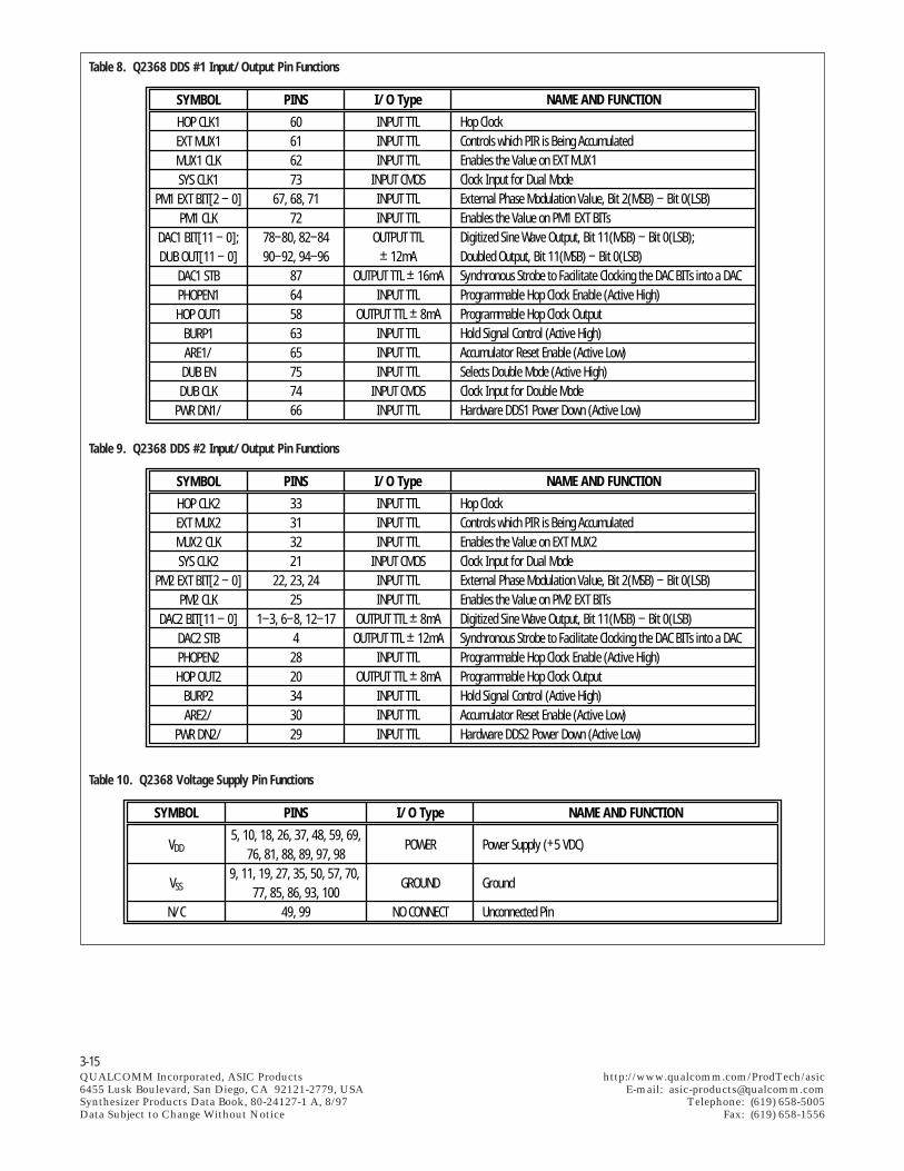
3-15QUALCOMM Incorporated, ASIC Products http://www.qualcomm.com/ProdTech/asic6455 Lusk Boulevard, San Diego, CA 92121-2779, USA E-mail: [email protected] Products Data Book, 80-24127-1 A, 8/97 Telephone: (619) 658-5005Data Subject to Change Without Notice Fax: (619) 658-1556
SYMBOL
VDD
VSS
N/C
PINS
5, 10, 18, 26, 37, 48, 59, 69,76, 81, 88, 89, 97, 98
9, 11, 19, 27, 35, 50, 57, 70, 77, 85, 86, 93, 100
49, 99
I/O Type
POWER
GROUND
NO CONNECT
NAME AND FUNCTION
Power Supply (+5 VDC)
Ground
Unconnected Pin
Table 10. Q2368 Voltage Supply Pin Functions
SYMBOL
HOP CLK1EXT MUX1MUX1 CLKSYS CLK1
PM1 EXT BIT[2 – 0]PM1 CLK
DAC1 BIT[11 – 0];DUB OUT[11 – 0]
DAC1 STBPHOPEN1HOP OUT1
BURP1ARE1/DUB ENDUB CLK
PWR DN1/
PINS
60616273
67, 68, 7172
78–80, 82–8490–92, 94–96
8764586365757466
I/O Type
INPUT TTLINPUT TTLINPUT TTL
INPUT CMOSINPUT TTLINPUT TTL
OUTPUT TTL± 12mA
OUTPUT TTL ± 16mAINPUT TTL
OUTPUT TTL ± 8mAINPUT TTLINPUT TTLINPUT TTL
INPUT CMOSINPUT TTL
NAME AND FUNCTION
Hop ClockControls which PIR is Being AccumulatedEnables the Value on EXT MUX1Clock Input for Dual ModeExternal Phase Modulation Value, Bit 2(MSB) – Bit 0(LSB)Enables the Value on PM1 EXT BITsDigitized Sine Wave Output, Bit 11(MSB) – Bit 0(LSB);Doubled Output, Bit 11(MSB) – Bit 0(LSB)Synchronous Strobe to Facilitate Clocking the DAC BITs into a DACProgrammable Hop Clock Enable (Active High)Programmable Hop Clock OutputHold Signal Control (Active High)Accumulator Reset Enable (Active Low)Selects Double Mode (Active High)Clock Input for Double ModeHardware DDS1 Power Down (Active Low)
SYMBOL
HOP CLK2EXT MUX2MUX2 CLKSYS CLK2
PM2 EXT BIT[2 – 0]PM2 CLK
DAC2 BIT[11 – 0]DAC2 STBPHOPEN2HOP OUT2
BURP2ARE2/
PWR DN2/
PINS
33313221
22, 23, 2425
1–3, 6–8, 12–1742820343029
I/O Type
INPUT TTLINPUT TTLINPUT TTL
INPUT CMOSINPUT TTLINPUT TTL
OUTPUT TTL ± 8mAOUTPUT TTL ± 12mA
INPUT TTLOUTPUT TTL ± 8mA
INPUT TTLINPUT TTLINPUT TTL
NAME AND FUNCTION
Hop ClockControls which PIR is Being AccumulatedEnables the Value on EXT MUX2Clock Input for Dual ModeExternal Phase Modulation Value, Bit 2(MSB) – Bit 0(LSB)Enables the Value on PM2 EXT BITsDigitized Sine Wave Output, Bit 11(MSB) – Bit 0(LSB)Synchronous Strobe to Facilitate Clocking the DAC BITs into a DACProgrammable Hop Clock Enable (Active High)Programmable Hop Clock OutputHold Signal Control (Active High)Accumulator Reset Enable (Active Low)Hardware DDS2 Power Down (Active Low)
Table 8. Q2368 DDS #1 Input/Output Pin Functions
Table 9. Q2368 DDS #2 Input/Output Pin Functions
3-16QUALCOMM Incorporated, ASIC Products http://www.qualcomm.com/ProdTech/asic6455 Lusk Boulevard, San Diego, CA 92121-2779, USA E-mail: [email protected] Products Data Book, 80-24127-1 A, 8/97 Telephone: (619) 658-5005Data Subject to Change Without Notice Fax: (619) 658-1556
SIGNALS COMMON FOR BOTH DDSsThe following signals are used in common for both
DDS functions on the Q2368.
DATA0…DATA7INPUTS (52, 53, 54, 41, 39, 38, 40, 36)
8-bit data bus for writing values to the on-chip
processor interface registers. This bus is used for write
operations only. DATA0 is the LSB.
ADDRESS0…ADDRESS5INPUTS (47, 46, 45, 44, 43, 42)
6-bit address bus to select the internal processor
interface registers. Addresses must be held fixed
during the active period of the WR/ signal.
ADDRESS0 is the LSB.
CS/INPUT (55)
Chip Select. Must be held “Low” during processor
write accesses to the Q2368. Can be held “Low” all
the time, if desired.
WR/INPUT (56)
When “Low” while CS/ is “Low”, writes the value of
the data bus to the register determined by the address
bus.
SER CLKINPUT (52)
Serial Data Clock. Shifts serial data into SDATA IN
with each falling edge.
BUSSELECTINPUT (51)
Bus Select. A logic “Low” sets Q2368 for control via
8-bit Bus Mode. A logic “High” sets for control via
Serial Bus Mode.
VSS
INPUT (9, 11, 19, 27, 35, 50, 57, 70, 77, 85, 86, 93, 100)
Provides electrical ground reference for signal and
power inputs.
VDD
INPUT (5, 10, 18, 26, 37, 48, 59, 69, 76, 81, ,88, 89, 97, 98)
Provides power to all Q2368 circuitry.
N/CINPUT (49, 99)
These pins are unconnected.
SIGNALS INDEPENDENT FOR EACH DDSThe following signals pertain to a specific DDS
function (1 or 2) on the Q2368.
SDATA IN1, SDATA IN2INPUTS (54, 40)
Serial Data Input. Data is shifted in serially on falling
edge of SER CLK. The data format is with the most
significant bit (MSB) first.
SENABLE1, SENABLE2INPUTS (53, 38)
Serial Shift Enable. Active “High” control for loading
input serial data, SDATA IN.
SDATA OUT1, SDATA OUT2OUTPUTS (41, 36)
Serial Data Output. Provided for each DDS to enable
daisy-chaining of DDS1 to DDS2, or other serial-
controlled devices.
SYS CLK1, SYS CLK2INPUT (73, 21)
Provides the fundamental clock frequency of the
synthesized sine waveform when operating in Dual
Mode. Internal operations of the phase accumulator,
external phase modulation, and phase increment
registers for each respective DDS are synchronized to
this clock signal.
DUB ENINPUT (75)
Double Mode Enable. The Double Mode is activated
when the DUB EN input is set to a logic “High”.
Enabling DUB EN activates the DUB CLK input which
is the clock source input for Double Mode operation.
3-17QUALCOMM Incorporated, ASIC Products http://www.qualcomm.com/ProdTech/asic6455 Lusk Boulevard, San Diego, CA 92121-2779, USA E-mail: [email protected] Products Data Book, 80-24127-1 A, 8/97 Telephone: (619) 658-5005Data Subject to Change Without Notice Fax: (619) 658-1556
Setting DUB EN to a logic “Low” disables the DUB
CLK input and configures the Q2368 for Dual Mode
operation. (See Double Mode Operation section under
Internal Architecture .)
DUB CLKINPUT (74)
Provides the fundamental clock reference of the
synthesized sine waveform when operating in Double
Mode. Internal operations of the phase accumulators,
external phase modulation and phase increment
registers for both DDSs are synchronized to one-half
the rate of this clock signal. Therefore, although the
DUB CLK is a single clock source for the multiplexing
of both DDSs, all DDS operations are performed and
implemented with respect to the internal system clock
rate of DUB CLK/2. (See Double Mode Operation
section under Internal Architecture .)
HOP CLK1, HOP CLK2INPUT (60, 33)
The HOP CLK signal controls the activation of the
selection of the double buffered registers programmed
via the 8-bit bus or serial bus interface. HOP CLK
must be active “High” for at least one SYS CLK period
or two DUB CLK periods. It can be asserted once every
four SYS CLK periods, or eight DUB CLK periods.
HOP OUT1, HOP OUT2OUTPUTS (58, 20)
While operating in the Programmable Hop Clock
Mode, an output pulse is generated at the HOP OUT
pin when the programmable hop clock resets itself
according to its programmed time interval, TPHC. This
is useful for designing systems which are
synchronously locked to the DDS system clock or
require precise triggering of other system events with
DDS operations. The HOP OUT signal is a positive
pulse, one DDS system clock cycle wide. If the HOP
OUT signal is unused when operating in the
Programmable Hop Clock Mode, this output should be
terminated into an RC-type termination. This will
ensure that any potential for the repeating HOP OUT
pulse to radiate noise or corrupt other circuit areas is
filtered out.
PHOPEN1, PHOPEN2INPUTS (64, 28)
Programmable Hop Clock Enable. The Programmable
Hop Clock Mode is armed when the PHOPEN input is
set to a logic “High”. This mode activates a
programmable 32-bit duration counter (PHC register)
derived from the DDS system clock to produce the
PHC time period, TPHC . The next time the hop clock
signal is asserted, the PHC register is activated. (See
Programmable Hop Clock Enable (PHCE) section
under SMC Register.) The Programmable Hop Clock
Mode will be disabled when the PHOPEN input is set
to a logic “Low” and a hop clock signal is reasserted.
BURP1, BURP2INPUTS (63, 34)
The Q2368’s BURP control function allows instant
interruption of operating modes to produce a
stationary (fixed) output. BURP control is active when
it is set to a logic “High”. When operating in the
Chirp Mode, enabling the BURP signal will produce a
constant output frequency corresponding to the exact
position of where the chirp waveform was interrupted.
Enabling the BURP signal during any other non-chirp
DDS mode of operation (i.e., fixed frequency or phase
modulation) will result in a zero frequency (DC)
output, as in a burst-mode fashion, until the BURP
signal is disabled (set to a logic “Low”). In the same
manner, the Programmable Hop Clock Mode is
simultaneously interrupted (if it is active) when the
BURP signal is enabled. This allows the programmed
time interval, TPHC, to be maintained and resume
counting the PHC time period as soon as the BURP
signal is disabled. Moreover, all DDS operations
transition in a phase-continuous fashion when the
BURP control is enabled or disabled making it
attractive for many generic functions such as burst-
mode, auto-scan, or seek control. (Additional
reference is found under Modes of Operation in the
Chirp Mode section.)
3-18QUALCOMM Incorporated, ASIC Products http://www.qualcomm.com/ProdTech/asic6455 Lusk Boulevard, San Diego, CA 92121-2779, USA E-mail: [email protected] Products Data Book, 80-24127-1 A, 8/97 Telephone: (619) 658-5005Data Subject to Change Without Notice Fax: (619) 658-1556
ARE1/, ARE2/INPUTS (65, 30)
Accumulator Reset Enable. Each DDS function on the
Q2368 includes an accumulator reset register (ARR)
and an external accumulator reset which is applied to
the ARE/ input pin. By setting the ARE/ input to a
logic “Low”, the accumulator reset function is armed.
The next time the hop clock signal is asserted, all
activated phase accumulators are reset to zero. (See
Accumulator Reset Register (ARR) section.)`
PWR DN1/, PWR DN2/INPUTS (66, 29)
Power-down Enable. The Power-down Mode is armed
when the PWR DN/ input is set to a logic “Low”.
This function provides independent power-down
control for each DDS when operating in Dual Mode, or
a combined power-down function while operating the
Q2368 as one DDS in Double Mode. The next time
the hop clock signal is asserted, DDS current
consumption is reduced to within the 0.1 to 20 mA
range, depending on the clock frequency and whether
the device is operating in Dual Mode or Double Mode.
(See Table 3 for current consumption with different
operating conditions.) When the Q2368 is operating in
double mode, hardware control of power-down requires
both PWR DN/ signals to be set to a logic “Low” in
order to apply a complete power-down condition. All
data residing in the programming registers is retained
during power-down, although new information can
still be addressed via the processor interface. (See
PWDE section under SMC Register .) The Power-down
Mode will be disabled when the PWR DN/ input is set
to a logic “High” and a hop clock signal is reasserted.
When power-down is disabled and the DDSs are
activated to a power-up condition, previous phase
continuity will not be maintained, although the DDS
can be put into a known state by loading an
accumulator reset along with the desired frequency
and modulation mode commands.
EXT MUX1, EXT MUX2INPUT (61, 31)
When latched into the DDS with the signal MUX1
CLK (or MUX2 CLK) this signal determines whether
PIRA or PIRB will be used for the incremental phase
accumulator input value. When the EXT MUX signal
is set to “1”, the value stored in PIRB will be used by
the phase accumulator. When the EXT MUX signal is
set to “0”, the value stored in PIRA will be used.
MUX1 CLK, MUX2 CLKINPUT (62, 32)
The rising edge of this signal latches and enables the
value on the EXT MUX inputs. This signal must be
held “High” for a minimum of three SYS CLK periods,
or six DUB CLK periods. Activation of the EXT MUX
inputs is synchronized internally to the system clock.
PM1 EXT BIT0…PM1 EXT BIT2, PM2 EXT BIT0…PM2 EXT BIT2INPUTS (67, 68, 71, 22, 23, 24)
External phase modulation inputs which control 45
degree phase offsets in the phase accumulated values
in accordance with the settings provided in Table 6.
PM EXT BITs are active when the signal PM CLK is
asserted and are synchronized internally to the system
clock.
PM1 CLK, PM2 CLKINPUT (72, 25)
The rising edge of this signal latches and enables the
value on the PM EXT BIT inputs. This signal must be
held “High” for a minimum of three SYS CLK periods,
or six DUB CLK periods. The PM EXT BIT inputs are
synchronized internally to the system clock.
DAC1 BIT0…DAC1 BIT11, DAC2 BIT0…DAC2 BIT11OUTPUTS (96, 95, 94, 92, 91, 90, 84, 83, 82, 80, 79, 78, 17, 16, 15, 14,
13, 12, 8, 7, 6, 3, 2, 1)
Digitized sine wave outputs when operating in Dual
Mode. Encoded in offset binary or two’s complement
format, depending on settings in the AMC Registers.
One sample is generated during each period of SYS
CLK. DAC BIT 0 is the LSB.
3-19QUALCOMM Incorporated, ASIC Products http://www.qualcomm.com/ProdTech/asic6455 Lusk Boulevard, San Diego, CA 92121-2779, USA E-mail: [email protected] Products Data Book, 80-24127-1 A, 8/97 Telephone: (619) 658-5005Data Subject to Change Without Notice Fax: (619) 658-1556
DAC1 STB, DAC2 STBOUTPUT (87, 4)
Provides a synchronous strobe to facilitate clocking of
the DAC BIT outputs (or DUB OUT outputs) into an
external register or sampled DAC. One DAC STB is
generated during each period of SYS CLK or DUB CLK.
Essentially, the DAC STB (or DAC STB/) is a delayed
version of the system clock. A low-value series
resistor (100 Ω value typical) connected between this
output and the DAC’s clock input is recommended to
mitigate noise feedthrough from the high energy
switching transients on these pulses.
DUB OUT0...DUB OUT11OUTPUTS (96, 95, 94, 92, 91, 90, 84, 83, 82, 80, 79, 78)
Digitized sine wave outputs when operating in Double
Mode. Encoded in offset binary or 2’s complement
format, depending on settings in the AMC register.
One sample is generated during each period of DUB
CLK. DUB OUT0 is the LSB.
MODES OF OPERATIONEach DDS can be independently set to perform a wide
range of expanded functions of the basic operation, as
described in the following paragraphs. Control of all
functions apply identically for Double Mode operation.
(See Double Mode Operation section under Internal
Architecture .)
BASIC SYNTHESIZER MODEIn its most Basic Operational Mode, each DDS on the
Q2368 can provide a fixed frequency digitized sine
wave output. The frequency of this sine output is
determined by the frequency of the clock input and
the value stored in the PIRs. (See formula (1) in the
Phase Increment Value section.)
To set the Q2368 up in a single frequency output
mode, the SMC should be set to “00” (hex). The
AMC should be set according to the size of the DAC
selected and the desired output format. The PMAE
bit should also be set to “0” and the DAC STB bit set
to provide the best DAC triggering. (Reference the
Simple Oscillator Mode example section.)
PHASE MODULATION MODEThe Q2368 provides two means to implement phase
modulation of a basic frequency output, referred to as
Internal Phase Modulation and External Phase
Modulation.
Internal Phase Modulation provides extremely fine
resolution up to 0.00000008° of the phase adjustment
(232 - state phase resolution), while External Phase
Modulation is designed for 45° increment phase shifts.
INTERNAL PHASE MODULATIONInternal Phase Modulation operates as a differential
phase adjustment technique and requires use of the
processor interface. The Internal Phase Modulation
Mode is activated by loading PIRA with the correct
phase increment for the basic frequency without phase
modulation. PIRB is then loaded with the phase
increment value equal to the phase increment value
stored in PIRA plus the value of the desired phase
offset. The phase accumulator uses PIRA for most
phase accumulations.
Setting the HPME bit in the SMC register to logic
“1” arms the DDS to use the 32-bit value in PIRB for
one phase accumulation cycle when the hop clock
signal is asserted. Since the phase increment value in
PIRB is only used once for each hop clock assertion,
the net effect is to cause a phase change to the
generated sine wave.
When the PMAE bit is set to logic “1”, the 8 MSB of
PIRB are added to the 8 MSB of PIRA to form the
8 MSB to be accumulated with the 24 LSB of PIRA.
This 32-bit value is used for one-time accumulation. If
PMAE is “0”, all 32 units of PIRB will be used for the
accumulation.
The one-time phase shift occurs every time the hop
clock signal is asserted and can occur as often as the
hop clock signal can be asserted. (See Timing
Specifications section.)
If it is desired to change the phase offset value, PIRB
must be reloaded with the new phase offset before the
next hop clock cycle. The HPME bit will remain set to
“1” until reset by the processor. (Reference the Hop
Clock Phase Modulation Enable section.)
In general, the formula for calculating the phase
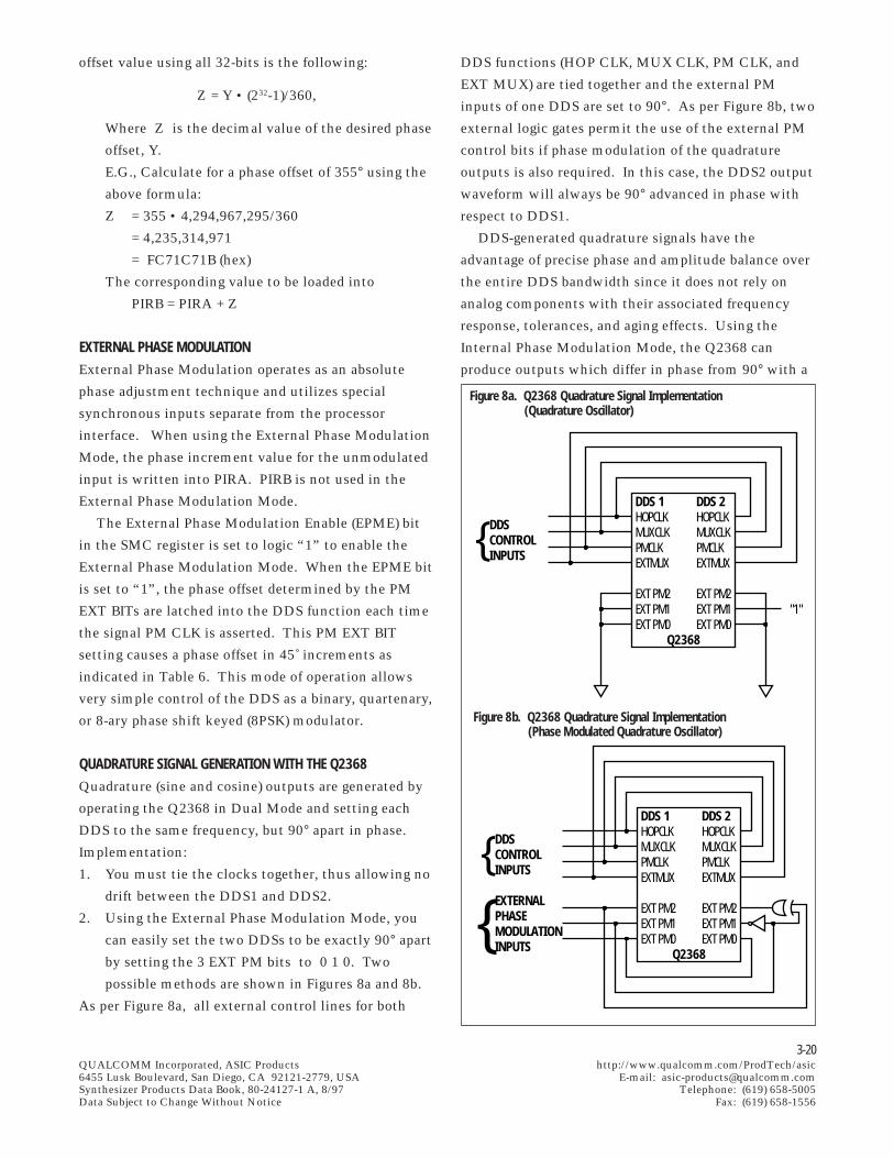
3-20QUALCOMM Incorporated, ASIC Products http://www.qualcomm.com/ProdTech/asic6455 Lusk Boulevard, San Diego, CA 92121-2779, USA E-mail: [email protected] Products Data Book, 80-24127-1 A, 8/97 Telephone: (619) 658-5005Data Subject to Change Without Notice Fax: (619) 658-1556
offset value using all 32-bits is the following:
Z = Y • (232-1)/360,
Where Z is the decimal value of the desired phase
offset, Y.
E.G., Calculate for a phase offset of 355° using the
above formula:
Z = 355 • 4,294,967,295/360
= 4,235,314,971
= FC71C71B (hex)
The corresponding value to be loaded into
PIRB = PIRA + Z
EXTERNAL PHASE MODULATIONExternal Phase Modulation operates as an absolute
phase adjustment technique and utilizes special
synchronous inputs separate from the processor
interface. When using the External Phase Modulation
Mode, the phase increment value for the unmodulated
input is written into PIRA. PIRB is not used in the
External Phase Modulation Mode.
The External Phase Modulation Enable (EPME) bit
in the SMC register is set to logic “1” to enable the
External Phase Modulation Mode. When the EPME bit
is set to “1”, the phase offset determined by the PM
EXT BITs are latched into the DDS function each time
the signal PM CLK is asserted. This PM EXT BIT
setting causes a phase offset in 45˚ increments as
indicated in Table 6. This mode of operation allows
very simple control of the DDS as a binary, quartenary,
or 8-ary phase shift keyed (8PSK) modulator.
QUADRATURE SIGNAL GENERATION WITH THE Q2368Quadrature (sine and cosine) outputs are generated by
operating the Q2368 in Dual Mode and setting each
DDS to the same frequency, but 90° apart in phase.
Implementation:
1. You must tie the clocks together, thus allowing no
drift between the DDS1 and DDS2.
2. Using the External Phase Modulation Mode, you
can easily set the two DDSs to be exactly 90° apart
by setting the 3 EXT PM bits to 0 1 0. Two
possible methods are shown in Figures 8a and 8b.
As per Figure 8a, all external control lines for both
DDS functions (HOP CLK, MUX CLK, PM CLK, and
EXT MUX) are tied together and the external PM
inputs of one DDS are set to 90°. As per Figure 8b, two
external logic gates permit the use of the external PM
control bits if phase modulation of the quadrature
outputs is also required. In this case, the DDS2 output
waveform will always be 90° advanced in phase with
respect to DDS1.
DDS-generated quadrature signals have the
advantage of precise phase and amplitude balance over
the entire DDS bandwidth since it does not rely on
analog components with their associated frequency
response, tolerances, and aging effects. Using the
Internal Phase Modulation Mode, the Q2368 can
produce outputs which differ in phase from 90° with a
Figure 8a. Q2368 Quadrature Signal Implementation (Quadrature Oscillator)
DDS 1HOPCLKMUXCLKPMCLKEXTMUX
EXT PM2EXT PM1EXT PM0
Q2368
DDS 2HOPCLKMUXCLKPMCLKEXTMUX
EXT PM2EXT PM1EXT PM0
"1"
DDSCONTROLINPUTS
Figure 8b. Q2368 Quadrature Signal Implementation (Phase Modulated Quadrature Oscillator)
DDS 1HOPCLKMUXCLKPMCLKEXTMUX
EXT PM2EXT PM1EXT PM0
Q2368
DDS 2HOPCLKMUXCLKPMCLKEXTMUX
EXT PM2EXT PM1EXT PM0
DDSCONTROLINPUTSEXTERNALPHASEMODULATIONINPUTS
3-21QUALCOMM Incorporated, ASIC Products http://www.qualcomm.com/ProdTech/asic6455 Lusk Boulevard, San Diego, CA 92121-2779, USA E-mail: [email protected] Products Data Book, 80-24127-1 A, 8/97 Telephone: (619) 658-5005Data Subject to Change Without Notice Fax: (619) 658-1556
minimum resolution of 360°/232. Since a
microprocessor-controlled system can store open-loop
compensation data vs. frequency, phase compensation
can be made as an adjustment during equipment
calibration. Alternatively, a closed-loop system can be
constructed, given a suitable detector, which will
allow feedback control of fine resolution offsets from
quadrature for compensation of phase errors elsewhere
in the system.
BINARY FREQUENCY SHIFT KEYING (BFSK)MODULATION MODETwo PIRs are provided for each DDS function allowing
for Binary Frequency Shift Keyed (BFSK) modulation
without any additional hardware. The Q2368 provides
signals allowing this switch to occur synchronously.
BFSK Modulation is achieved by setting the phase
increment value in PIRA to generate the first
frequency and the value in the PIRB to generate the
second frequency. The EME bit in the SMC register is
then set to logic “1” to enable the external multiplexer
controls.
If the EXT MUX signal is set to logic “1” when the
MUX CLK signal is asserted, the phase accumulator
will choose the phase increment value from PIRB. If
the EXT MUX signal is set to logic “0” when the MUX
CLK is asserted, the phase accumulator will choose the
phase increment value from PIRA. Changing the
value of the EXT MUX input causes the alternation
between the frequency controlled by PIRA and the
frequency controlled by PIRB.
After the BFSK Mode is set up and the PIRA and
PIRB contents are active, the EXT MUX signal can be
changed as fast as the MUX CLK can be asserted. (See
External Control Timing shown in Figure 20 and
Table 18.) The MUX CLK timing is the only
restriction on how fast the accumulation can be
switched from PIRA to PIRB.
MINIMUM SHIFT KEYING (MSK) MODULATION MODEThe Minimum Shift Keying (MSK) Modulation Mode
is a subset of the BFSK Mode described above. The
operation is the same, but the two frequencies are
selected at a known mathematically determined rate.
The MSK Modulation Mode is linear MSK and can be
generated by setting the frequency shift rate equal to
the separation between the two frequencies. This is
where MSK got its name, since it is the minimum
spacing between the two frequencies that can be
accomplished while still recovering the signal with a
given shift rate. If the frequency spacing is closer than
the frequency shift rate, the information cannot be
recovered. If the spacing is too far apart, the
information can be retrieved using FSK demodulation
techniques, although MSK will not be generated from
the resultant spectra. To produce the two MSK
frequencies, the values in PIRA and PIRB correspond to
incrementing and decrementing phase values
(respectively) that must change through ±90 degrees for
each symbol time of the frequency shift rate. This is
obtained by loading PIRA and PIRB with frequency
values such that the mid-point value between them is
separated by ± FSK rate/2. This must occur without
any phase discontinuities but since the DDS changes
frequencies in a phase continuous fashion, this is not a
problem. The overall result due to the slow phase
transitions between the frequencies is a reduction in
the high-frequency spectral content, thus attenuating
the sidelobes. The spectrum is said to be more
efficient since more power is contained in the main
lobe and less in the sidelobes. The EME bit of the
SMC register is set to logic “1”, as in the BFSK Mode,
and the EXT MUX and MUX CLK signals control the
shift between the values of PIRA and PIRB.
FREQUENCY HOPPING MODESimple frequency hopping can be enabled by writing a
new phase increment value of the desired frequency in
PIRA. Since PIRA is a double buffered register, this
value will be activated at the next assertion of the hop
clock signal.
Assuming each frequency to be generated requires
all 32 bits to be changed, then four 8-bit writes to PIRA
would be needed if programming via 8-bit bus control
is used. After PIRA has been loaded, the assertion of
the hop clock will activate these settings and the
resulting frequency will be output from the Q2368
within 32 clock cycles. The frequency value can be
3-22QUALCOMM Incorporated, ASIC Products http://www.qualcomm.com/ProdTech/asic6455 Lusk Boulevard, San Diego, CA 92121-2779, USA E-mail: [email protected] Products Data Book, 80-24127-1 A, 8/97 Telephone: (619) 658-5005Data Subject to Change Without Notice Fax: (619) 658-1556
changed as fast as the new phase increment value can
be written to PIRA and a hop clock signal asserted.
Once all 32 bits have been activated, the contents will
remain until the register is written again. Subsets
within the register may also be written. This allows
for the changing of an existing register value using a
single 8-bit write as opposed to four 8-bit writes, if
programming via 8-bit bus control is used.
CHIRP MODEThe Q2368 implements an additional mode in which
a second-order phase accumulator process is used to
implement a linearly changing frequency output. In
this mode, the output frequency changes at a constant
rate in an increasing or decreasing frequency direction.
This linear frequency sweep mode is referred to as a
“chirp” output. A chirp output can be described in
terms of a start and stop frequency (F0 and F1 ,
respectively) and the time it takes for the signal to
travel between the two frequencies (τ).
CHIRP WAVEFORM VARIATIONSThe Q2368 can be operated to perform various chirp
waveform sequences which will be determined by the
actual design requirements involved. As an example,
the chirp output can begin at F0 as an upward ramping
signal to F1. When the signal reaches the stopping
frequency, F1 , after τ seconds, the waveform can be
controlled in many fashions as illustrated in Figure 9:
1. The signal can stop at F1 and produce a constant F1
value.
2. The signal can repeat itself, thus producing a
sawtooth waveform.
3. The signal can begin a downramping waveform
from F1. When the signal reaches F0, it can begin
ramping up again (triangular waveform).
4. The signal can be reset to 0 (zero) frequency and
phase to stop the output.
CHIRP IMPLEMENTATIONThe Chirp Mode requires two phase accumulators,
cascaded serially, to create the linearly changing
frequency output. To generate a chirp waveform, a
linear frequency change is added to the first phase
accumulator to produce an instantaneous frequency, f.
The first accumulator’s output is then integrated by
the second accumulator to produce an instantaneous
phase, φ = ∫ fdt.
PROGRAMMABLE CHIRP RATE (PCR)This feature provides for independent control of the
chirp sweep rate and the output frequency. The
limitations on the resolution of the sweep rate come
from the system clock frequency and the size of the
phase accumulator. The chirp rate control was
implemented to allow the user to vary the slope of the
chirp signal by varying the clock frequency used in
the Chirp Mode. The programmable chirp rate
introduces a 20-bit counter (PCR register) derived
from the DDS clock reference to produce the chirp
rate clock , FPCR , for Accumulator A. In conjunction
with the phase increment value in PIRA, this is used
by the Q2368 to achieve < 1Hz/sec minimum chirp
sweep rate over the entire clock speed range.
PIECEWISE LINEAR CHIRPAs mentioned earlier, if a strictly linear sweep is
desired, the chirp output can be described in terms of
a start and stop frequency and the time (τ) it takes for
the signal to travel between the two frequencies, as
shown in Figure 10. Alternatively, if the desired
output response cannot be implemented in one chirp
waveform, the programmable chirp rate control can be
used to dynamically adjust the slope of the chirp
response to achieve a near-parabolic or piecewise
linear frequency output, as shown in Figure 11. This
requires the assertion of a hop clock signal to affect
the change in the PCR register which will change theTimeτ0
F0
F1
Frequency
∆F
1
2
3
4
Figure 9. Q2368 Examples of Chirp Waveforms
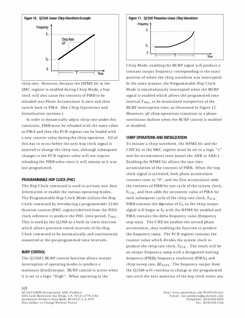
3-23QUALCOMM Incorporated, ASIC Products http://www.qualcomm.com/ProdTech/asic6455 Lusk Boulevard, San Diego, CA 92121-2779, USA E-mail: [email protected] Products Data Book, 80-24127-1 A, 8/97 Telephone: (619) 658-5005Data Subject to Change Without Notice Fax: (619) 658-1556
F0
F1
τ
Chirp Rate∆F
Frequency
Time0
F0
F1
τ
Frequency
Time0
Chirp Mode, enabling the BURP signal will produce a
constant output frequency corresponding to the exact
position of where the chirp waveform was interrupted.
In the same manner, the Programmable Hop Clock
Mode is simultaneously interrupted when the BURP
signal is enabled which allows the programmed time
interval,TPHC, to be maintained irrespective of the
BURP interruption time, as illustrated in Figure 12.
Moreover, all chirp operations transition in a phase-
continuous fashion when the BURP control is enabled
or disabled.
CHIRP OPERATIONS AND INITIALIZATIONTo initiate a chirp waveform, the HPME bit and the
CHE bit in the SMC register must be set to a logic “1”
and the accumulators reset (assert the ARR or ARE/).
Enabling the HPME bit allows the one time
accumulation of the contents of PIRB. When the hop
clock signal is activated, both phase accumulator
contents reset to “0”, and the first accumulator adds
the contents of PIRB for one cycle of the system clock,
FCLK , and then adds the increment value of PIRA for
each subsequent cycle of the chirp rate clock, FPCR.
PIRB contains the ∆φ value of F0, so the chirp output
signal will begin at F0 with the HPME bit enabled and
PIRA contains the delta frequency value (frequency
step size). The CHE bit enables the second phase
accumulator, thus enabling the function to produce
the frequency ramp. The PCR register contains the
counter value which divides the system clock to
produce the chirp rate clock, FPCR . The result will be
an output frequency ramp with a designated starting
frequency (PIRB), frequency resolution (PIRA), and
chirp sweep rate, ∆FRATE. The frequency output from
the Q2368 will continue to change at the programmed
rate until the next assertion of the hop clock resets any
Figure 10. Q2368 Linear Chirp Waveform Example Figure 11. Q2368 Piecewise-Linear Chirp Waveform
chirp rate. However, because the HPME bit in the
SMC register is enabled during Chirp Mode, a hop
clock will also cause the contents of PIRB to be
reloaded into Phase Accumulator A once and then
switch back to PIRA. (See Chirp Operations and
Initialization sections.)
In order to dynamically adjust chirp rate under this
constraint, PIRB must be reloaded with the same value
as PIRA and then the PCR register can be loaded with
a new counter value during the chirp operation. All of
this has to occur before the next hop clock signal is
asserted to change the chirp rate, although subsequent
changes to the PCR register value will not require
reloading the PIRB value since it will remain as it was
last programmed.
PROGRAMMABLE HOP CLOCK (PHC)The Hop Clock command is used to activate new data
information or enable the various operating modes.
The Programmable Hop Clock Mode utilizes the Hop
Clock command by introducing a programmable 32-bit
duration counter (PHC register) derived from the DDS
clock reference to produce the PHC time period, TPHC .
This is used by the Q2368 as a built-in timer function
which allows precision timed intervals of the Hop
Clock command to be automatically and continuously
reasserted at the pre-programmed time intervals.
BURP CONTROLThe Q2368’s BURP control function allows instant
interruption of operating modes to produce a
stationary (fixed) output. BURP control is active when
it is set to a logic “High”. When operating in the
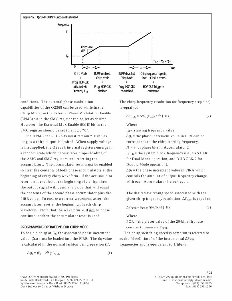
3-24QUALCOMM Incorporated, ASIC Products http://www.qualcomm.com/ProdTech/asic6455 Lusk Boulevard, San Diego, CA 92121-2779, USA E-mail: [email protected] Products Data Book, 80-24127-1 A, 8/97 Telephone: (619) 658-5005Data Subject to Change Without Notice Fax: (619) 658-1556
conditions. The external phase modulation
capabilities of the Q2368 can be used while in the
Chirp Mode, so the External Phase Modulation Enable
(EPME) bit in the SMC register can be set as desired.
However, the External Mux Enable (EME) bit in the
SMC register should be set to a logic “0”.
The HPME and CHE bits must remain “High” as
long as a chirp output is desired. When supply voltage
is first applied, the Q2368’s internal registers emerge in
a random state which necessitates proper loading of
the AMC and SMC registers, and resetting the
accumulators. The accumulator reset must be enabled
to clear the contents of both phase accumulators at the
beginning of every chirp waveform. If the accumulator
reset is not enabled at the beginning of a chirp, then
the output signal will begin at a value that will equal
the contents of the second phase accumulator plus the
PIRB value. To ensure a correct waveform, assert the
accumulator reset at the beginning of each chirp
waveform. Note that the waveform will not be phase
continuous when the accumulator reset is used.
PROGRAMMING OPERATIONS FOR CHIRP MODETo begin a chirp at F0, the associated phase increment
value (∆φ) must be loaded into the PIRB. The ∆φ value
is calculated in the normal fashion using equation (1),
∆φB = (F0 • 2N )/FCLK (1)
The chirp frequency resolution (or frequency step size)
is equal to:
∆FRES = ∆φA (FCLK /2N) Hz (2)
Where
F0 = starting frequency value.
∆φB = the phase increment value in PIRB which
corresponds to the chirp starting frequency.
N = # of phase bits in Accumulator 2
FCLK = the system clock frequency (i.e., SYS CLK
for Dual Mode operation, and DUB CLK/2 for
Double Mode operation).
∆φA = the phase increment value in PIRA which
controls the amount of output frequency change
with each Accumulator 1 clock cycle.
The desired switching speed associated with the
given chirp frequency resolution, ∆FRES, is equal to:
∆FPCR = FCLK /(PCR+1) Hz (3)
Where
PCR = the preset value of the 20-bit chirp rate
counter to generate FPCR.
The chirp switching speed is sometimes referred to
as the “dwell time” of the incremental ∆FRES
frequencies and is equivalent to 1/∆FPCR.
F0
F1
Chirp Rate∆F
Frequency
Time0
BURP disabled,Chirp Mode
+Prog. HOP CLK
re-enabled
BURP enabled,Chirp Mode
+Prog. HOP CLK
disabled
Chirp Mode+
Prog. HOP CLKactivated withDuration, TPHC
Chirp sequence repeats,Prog. HOP CLK resets
+HOP OUT Trigger is
generated
τ1 τ2
TPHC = τ1 + τ2
Figure 12. Q2368 BURP Function Illustrated
3-25QUALCOMM Incorporated, ASIC Products http://www.qualcomm.com/ProdTech/asic6455 Lusk Boulevard, San Diego, CA 92121-2779, USA E-mail: [email protected] Products Data Book, 80-24127-1 A, 8/97 Telephone: (619) 658-5005Data Subject to Change Without Notice Fax: (619) 658-1556
The chirp sweep rate (or chirp ramp rate) is equal to:
∆FRATE = ∆FRES • ∆FPCR
= ∆φA (FCLK)2/[(PCR+1) • 2N ] Hz/sec (4)
The smallest non-zero slope for a constant clock
period is obtained when the phase increment value in
PIRA = 1, resulting in a minimum sweep rate of:
∆FRATE minimum = (FCLK)2/[(PCR+1) • 2N ] Hz/sec (5)
The determination of the ∆FRATE parameters
ensures that the appropriate frequency rate will occur
between F0 and F1 in the specified duration, τ , as
redefined below:
∆FRATE = | F1 - F0 |/τ Hz/sec (6)
Since PIRA is used to store the frequency resolution
associated with the desired ramp, the value of ∆φA will
be an integer representing a multiple value of the
minimum resolution and hence determines the
frequency granularity of the corresponding chirp
waveform. This concept can be useful as a relative
measure in deciding how granular or “smooth” a chirp
waveform should be made for a given application. By
substituting in equations (4) and (6), the value of ∆φA
can also be determined as:
∆φA = [(PCR+1) • 2N • | F1 - F0 |] / [(FCLK)2 • τ] (7)
The specified duration, τ , over which a given chirp
sequence is directed, can be controlled very precisely
by the programmable hop clock. In this mode, the
32-bit PHC register is loaded with the corresponding
value to count the number of system clock periods
before another hop clock command gets automatically
issued and activates the latest instruction routine
programmed to follow. The preset value of the 32-bit
counter corresponding to the desired chirp duration is
determined using the following relation:
PHC = [(τ/TCLK) -1] (8)
Where
TCLK = 1/FCLK
τ = TPHC = the desired PHC time period
LIMITS ON THE CHIRP SEQUENCE DURATION, ττ has underlying restrictions that must be considered
when implementing a chirp output. The user must
make sure that the duration (τ) will be long enough so
the changes for the next output waveform can be
implemented before the chirp signal reaches its
stopping frequency. For example, if the user wants to
change the chirp to begin at a new frequency and have
a new stopping point, then the device must be reset to
do so. This change would require re-loading PIRA and
PIRB, which requires up to eight 8-bit write functions
using 8-bit bus control. The accumulator reset must
also be reset and a hop clock is needed to activate all of
the new settings. Therefore, τ must be set accordingly
to accommodate for the minimum timing needed to
make these changes.
CHANGING FROM A CHIRP WAVEFORM TO A NON-CHIRPWAVEFORMWhen the HPME bit is set to a logic “1”, the hop clock
signal is internally extended to two system clock
cycles. The two system clock cycles make it possible
for the phase accumulator to add the contents from
PIRB once, and then switch the process immediately
back to PIRA.
In order to change the output signal from a chirp to
a non-chirp waveform, the HPME bit and the CHE bit
in the SMC register must be disabled by setting them
to a logic “0”. The hop clock command is required to
initiate this change and during the HPME’s transition
from “1” to “0”, the hop clock signal is
correspondingly extended to two system clock cycles.
This results in an automatic switch of the
accumulation process back to PIRA. The CHE bit is
used for chirp waveform generation only and should be
disabled whenever a non-chirp waveform is desired. It
is necessary to reset the HPME to “0” in the case when
you want to stop Chirp Mode, or disable the Internal
Phase Modulation Mode and reconfigure operation to
the Basic Oscillator Mode, for example. If phase
offsetting control is desired, as in the case of operating
in the Internal Phase Modulation Mode, then the
HPME bit should remain set to a logic “1”.
Additionally, it is worth noting that while operating
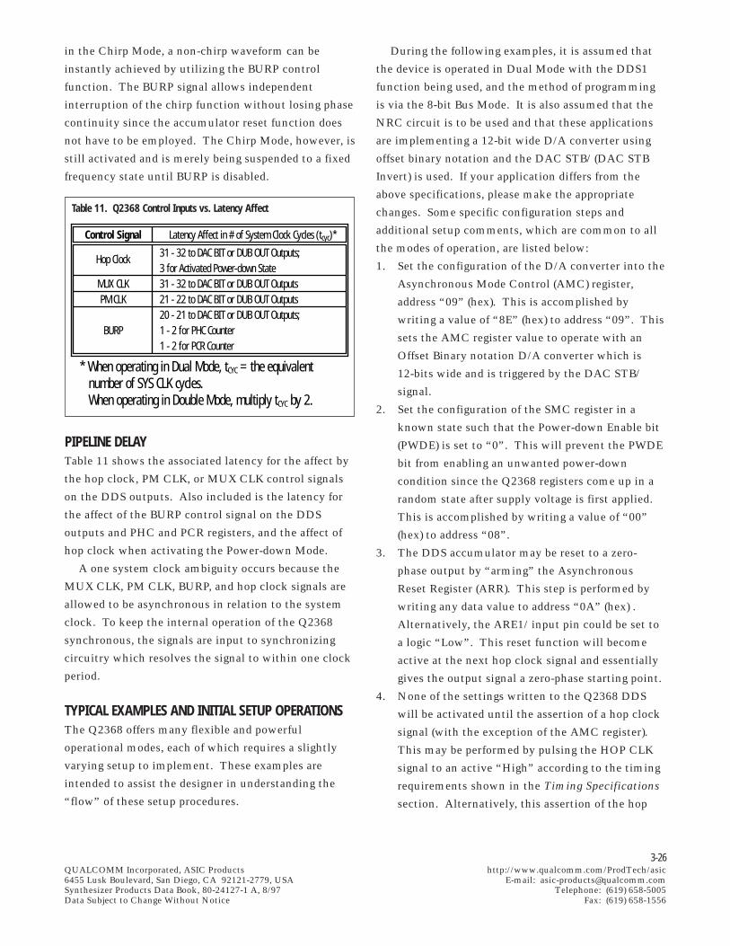
3-26QUALCOMM Incorporated, ASIC Products http://www.qualcomm.com/ProdTech/asic6455 Lusk Boulevard, San Diego, CA 92121-2779, USA E-mail: [email protected] Products Data Book, 80-24127-1 A, 8/97 Telephone: (619) 658-5005Data Subject to Change Without Notice Fax: (619) 658-1556
Control Signal
Hop Clock
MUX CLKPM CLK
BURP
Latency Affect in # of System Clock Cycles (tcyc)*
31 - 32 to DAC BIT or DUB OUT Outputs;3 for Activated Power-down State31 - 32 to DAC BIT or DUB OUT Outputs21 - 22 to DAC BIT or DUB OUT Outputs20 - 21 to DAC BIT or DUB OUT Outputs;1 - 2 for PHC Counter1 - 2 for PCR Counter
* When operating in Dual Mode, tCYC = the equivalent number of SYS CLK cycles. When operating in Double Mode, multiply tCYC by 2.
Table 11. Q2368 Control Inputs vs. Latency Affect
PIPELINE DELAYTable 11 shows the associated latency for the affect by
the hop clock, PM CLK, or MUX CLK control signals
on the DDS outputs. Also included is the latency for
the affect of the BURP control signal on the DDS
outputs and PHC and PCR registers, and the affect of
hop clock when activating the Power-down Mode.
A one system clock ambiguity occurs because the
MUX CLK, PM CLK, BURP, and hop clock signals are
allowed to be asynchronous in relation to the system
clock. To keep the internal operation of the Q2368
synchronous, the signals are input to synchronizing
circuitry which resolves the signal to within one clock
period.
TYPICAL EXAMPLES AND INITIAL SETUP OPERATIONSThe Q2368 offers many flexible and powerful
operational modes, each of which requires a slightly
varying setup to implement. These examples are
intended to assist the designer in understanding the
“flow” of these setup procedures.
During the following examples, it is assumed that
the device is operated in Dual Mode with the DDS1
function being used, and the method of programming
is via the 8-bit Bus Mode. It is also assumed that the
NRC circuit is to be used and that these applications
are implementing a 12-bit wide D/A converter using
offset binary notation and the DAC STB/ (DAC STB
Invert) is used. If your application differs from the
above specifications, please make the appropriate
changes. Some specific configuration steps and
additional setup comments, which are common to all
the modes of operation, are listed below:
1. Set the configuration of the D/A converter into the
Asynchronous Mode Control (AMC) register,
address “09” (hex). This is accomplished by
writing a value of “8E” (hex) to address “09”. This
sets the AMC register value to operate with an
Offset Binary notation D/A converter which is
12-bits wide and is triggered by the DAC STB/
signal.
2. Set the configuration of the SMC register in a
known state such that the Power-down Enable bit
(PWDE) is set to “0”. This will prevent the PWDE
bit from enabling an unwanted power-down
condition since the Q2368 registers come up in a
random state after supply voltage is first applied.
This is accomplished by writing a value of “00”
(hex) to address “08”.
3. The DDS accumulator may be reset to a zero-
phase output by “arming” the Asynchronous
Reset Register (ARR). This step is performed by
writing any data value to address “0A” (hex) .
Alternatively, the ARE1/ input pin could be set to
a logic “Low”. This reset function will become
active at the next hop clock signal and essentially
gives the output signal a zero-phase starting point.
4. None of the settings written to the Q2368 DDS
will be activated until the assertion of a hop clock
signal (with the exception of the AMC register).
This may be performed by pulsing the HOP CLK
signal to an active “High” according to the timing
requirements shown in the Timing Specifications
section. Alternatively, this assertion of the hop
in the Chirp Mode, a non-chirp waveform can be
instantly achieved by utilizing the BURP control
function. The BURP signal allows independent
interruption of the chirp function without losing phase
continuity since the accumulator reset function does
not have to be employed. The Chirp Mode, however, is
still activated and is merely being suspended to a fixed
frequency state until BURP is disabled.
3-27QUALCOMM Incorporated, ASIC Products http://www.qualcomm.com/ProdTech/asic6455 Lusk Boulevard, San Diego, CA 92121-2779, USA E-mail: [email protected] Products Data Book, 80-24127-1 A, 8/97 Telephone: (619) 658-5005Data Subject to Change Without Notice Fax: (619) 658-1556
clock signal may be performed by writing any data
value to the Asynchronous Hop Clock (AHC)
register (address “0B” (hex)).
SIMPLE OSCILLATOR MODEWhen using the Simple Oscillator Mode, the Q2368
DDS outputs a digitized sine wave at a fixed frequency
ranging from essentially D.C. to 1⁄2 the frequency of
SYS CLK. Practical limitations on anti-alias filtering
will limit the range of frequencies to a maximum of
approximately 40% of the SYS CLK frequency.
During the following example, the desired output
frequency is 1⁄4 of the SYS CLK frequency. That is, if
the SYS CLK frequency is 30 MHz, the desired output
frequency is 7.5 MHz. The following steps should be
followed:
1. Set the mode of the device to be the Simple
Oscillator Mode. Setting the operation mode is
accomplished by disabling all modes in the
Synchronous Mode Control (SMC) register,
address 08(hex). In this case, the value of “00”
(hex) should be loaded into this device. This is
performed by setting the address bus (ADDRESS0
through ADDRESS5) to “08” and the data bus
(DATA0 through DATA7) to “00”. Set the Chip
Select signal (CS/) to active “0” and pulse the
Write Strobe (WR/) “Low” according to the timing
requirements shown in Figure 16 and Table 14.
The PMAE bit D6 of the AMC register is set to
“0” because the internal phase modulation
operation is disabled.
2. The actual phase increment value (32-bits) is next
loaded into the Phase Increment Register A
(PIRA), addresses “00” through “03” (hex). The
least significant byte of the 4-byte value is written
into address “00” and the most significant byte is
written into address “03”. The write operations
are performed using the process described in Step
1 and four. Such operations are required to load
all four byte-wide PIRA register addresses. For
this example of a desired output frequency which
is 1⁄4 of the SYS CLK frequency, the 32-bit value to
be written to PIRA is “40000000” (hex). In this
case, the registers at address “00”, “01”, and “02”
are written with a data value of “00” while address
“03” is written with a data value of “40” (hex).
3. The assertion of a hop clock signal will cause the
Q2368 to begin synthesizing an unmodulated sine
wave at a frequency equal to 1⁄4 the frequency of
the SYS CLK input.
BINARY FREQUENCY SHIFT KEYING (BFSK) MODEThe following procedure will initialize the Q2368 to
operate in the BFSK Mode. For this example, the
desired frequencies to be generated are 1⁄4 and 1⁄8 of the
SYS CLK frequency. That is, if the SYS CLK frequency
is 30 MHz, the desired output frequencies are 7.5 MHz,
and 3.75 MHz respectively.
It is assumed that the phase increment value
associated with generating 7.5 MHz will be stored in
PIRA and 3.75 MHz will be stored in PIRB. The
following steps should be followed:
1. Setting up the BFSK Mode is accomplished by
disabling all modes in the Synchronous Mode
Control (SMC) register, address “08” (hex) except
EXT MUX ENABLE (EME) bit D2. The EME bit
should be set to logic “1”. In this case, the value
of “04” (hex) should be loaded into this device.
This is performed by writing the address bus
(ADDRESS0 through ADDRESS5) with a data
value of “08” (hex) and the data bus (DATA0
through DATA7) with a data value of “04” (hex).
The PMAE bit D6 of the AMC register is set to “0”
because the internal phase modulation operation is
disabled.
2. The actual phase increment values (32-bits) are
loaded into their respective Phase Increment
Register. For PIRA, use addresses “00” through
“03” (hex) and for PIRB use addresses “04” through
“07” (hex). The least significant byte (LSB) of the
4-byte value is written into address “00” (PIRA) or
“04” (PIRB) and the most significant byte (MSB) is
written into address “03” (PIRA) or “07” (PIRB).
Since the phase increment registers are 32-bits
wide, four such operations are required to load all
four byte-wide PIRA and PIRB register addresses.
3-28QUALCOMM Incorporated, ASIC Products http://www.qualcomm.com/ProdTech/asic6455 Lusk Boulevard, San Diego, CA 92121-2779, USA E-mail: [email protected] Products Data Book, 80-24127-1 A, 8/97 Telephone: (619) 658-5005Data Subject to Change Without Notice Fax: (619) 658-1556
For this example, the 32-bit phase increment
value written to PIRA is “40000000” (hex). In this
case, the registers at address “00”, “01”, and “02”
are written with a data value of “00” while address
“03” is written with a data value of “40” (hex).
The 32-bit phase increment value to be written to
PIRB is “2000000” (hex). In this case, the registers
at address “04”, “05”, and “06” are written with a
data value of “00” while address “07” is written
with a data value of “20” (hex).
3. The EME bit is set to logic “1” to enable the
external multiplexer controls. This will make the
settings at the EXT MUX1 pin (pin 61) select
which PIR to use for accumulation purposes. If
EXT MUX1 is set to logic “1”, then PIRB will be
accumulated. If it is set to logic “0”, then the
contents of PIRA will be accumulated.
EXTERNAL PHASE MODULATION MODEWhen using the External Phase Modulation Mode, the
Q2368 DDS has the capability to shift its output signal
in 45° increments from 45° to 315°. Since the Q2368
is a dual device, it is ideal to use as a quadrature
oscillator because it requires only one Q2368 device;
this is further described in the Quadrature Signal
Generation section.
The following procedure will initialize the Q2368 to
operate in the External Phase Modulation Mode. The
desired phase shift will be 90° for this example (see
Table 6 for other phase settings) and the frequency to
be generated is 1⁄4 of the SYS CLK frequency. That is,
if the SYS CLK frequency is 30 MHz, the desired
output frequency is 7.5 MHz.
The following steps should be followed:
1. Setting the operation mode is accomplished by
disabling all modes in the Synchronous Mode
Control (SMC) register, address 08(hex) except EXT
PHASE MOD ENABLE (EPME) bit D1. The EPME
bit should be set to logic "1". In this case, the
value of “02” (hex) should be loaded into this
device. This is performed by writing the address
bus (ADDRESS0 through ADDRESS5) with a data
value of “08” and the data bus (DATA0 through
DATA7) with a data value of “02”. The PMAE bit
D6 of the AMC register is set to “0” because the
internal phase modulation operation is disabled.
2. The actual phase increment value (32-bits) is
loaded into the Phase Increment Register A (PIRA),
addresses “00” through “03” (hex). The least
significant byte (LSB) of the 4-byte value is written
into address “00” and the most significant byte
(MSB) is written into address “03”. The desired
output frequency is 1⁄4 of the SYS CLK frequency;
the 32-bit value to be written to PIRA is
“40000000” (hex). In this case, the registers at
address “00”, “01”, and “02” are written with a
data value of “00” while address “03” is written
with a data value of “40” (hex).
3. To affect the 90˚ phase shift, set PM1 EXT BIT2,
PM1 EXT BIT1, PM1 EXT BIT0 to 0 1 0
respectively. (See Table 6 for the settings.) These
inputs are latched into the DDS by pulsing the
signal PM1 CLK “High” according to the timing
specifications in Figure 20 and Table 18.
FREQUENCY HOPPING MODEThe example of frequencies to be hopped between are1⁄16, 1⁄8 and 1⁄4 of the SYS CLK frequency. That is, if the
SYS CLK frequency is 30 MHz, the desired frequencies
are 1.875 MHz, 3.75 MHz, and 7.5 MHz respectively.
It is assumed that the first frequency to be generated
will be 1.875 MHz, then 3.75 MHz and last 7.5 MHz.
The user can hop between as many different
frequencies as desired, however for example purposes
we will limit the number to three. The following steps
should be followed:
1. Setting the operation mode is accomplished by
disabling all modes in the Synchronous Mode
Control (SMC) register, address 08(hex). In this
case, the value of “00” (hex) should be loaded into
this device. This is performed by writing the
address bus (ADDRESS0 through ADDRESS5) with
a data value of “08” and the data bus (DATA0
through DATA7) with a data value of “00”. The
PMAE bit D6 of the AMC register is set to “0”
because the internal phase modulation operation is
disabled.
3-29QUALCOMM Incorporated, ASIC Products http://www.qualcomm.com/ProdTech/asic6455 Lusk Boulevard, San Diego, CA 92121-2779, USA E-mail: [email protected] Products Data Book, 80-24127-1 A, 8/97 Telephone: (619) 658-5005Data Subject to Change Without Notice Fax: (619) 658-1556
2. The actual phase increment value (32-bits) is
loaded into the Phase Increment Register A (PIRA),
addresses “00” through “03” (hex). The least
significant byte (LSB) of the 4-byte value is written
into address “00” and the most significant byte
(MSB) is written into address “03”. For this
example, three frequencies are to be generated in
succesion. The first 32-bit value to be written to
PIRA is “10000000” (hex). The second 32-bit
value to be written to PIRA is “20000000” (hex)
and the third is “40000000”. Note, that in this
case the last 24-bits of each three phase increment
values are the same. Once the first 32-bit value
has been written to the PIRA, all you have to do is
change the 8 MSB to generate the three designated
frequencies. (The 24 LSB will remain the same
until they are re-written and activated by the hop
clock signal.) In this case, initially the registers at
address “00”, “01”, and “02” are written with a
data value of “00” while address “03” is written
with a data value of “10” (hex). To hop from 1⁄16 to1⁄8 of the SYS CLK, address “03” is written with a
data value of “20” (hex). The same operation is
followed to hop between 1⁄8 and 1⁄4 of the SYS CLK
frequency: address “03” is written with a data
value of “40” (hex). If the hopping frequencies did
not have any bits in common, then all 32-bits of
PIRA would need to be re-written according to the
instructions above.
INTERNAL PHASE MODULATION MODEWhen using the Internal Phase Modulation Mode, the
Q2368 DDS has the capability to shift its output signal
in 84 nano-degree increments (360°/232) throughout
the complete 360° range. The phase shift can occur as
often as the HOP CLK signal can be asserted according
to the timing requirements shown in Figure 16 and
Table 14.
The following procedure will initialize the Q2368 to
operate in the Internal Phase Modulation Mode to
output a synchronous preset frequency and phase. The
intended starting phase offset will be 5° for this
example and the frequency to be generated is
19.14 MHz using a SYS CLK frequency of 50 MHz.
The following steps should be followed:
1. Setting the operation mode is accomplished by
disabling all modes in the Synchronous Mode
Control (SMC) register, address 08 (hex) except
HOP CLK PHASE MOD ENABLE (HPME) bit D3.
The HPME bit should be set to logic “1”. In this
case, the value of “08” (hex) should be loaded into
this device. This is performed by writing the
address bus (ADDRESS0 through ADDRESS5)
with a data value of “08” and the data bus (DATA0
through DATA7) with a data value of “08”.
2. The actual phase increment values (32-bits) are
loaded into their respective Phase Increment
Register. For PIRA, use addresses “00” through
“03” (hex) and for PIRB use addresses “04”
through “07” (hex). The least significant byte
(LSB) of the 4-byte value is written into address
“00” (PIRA) or “04” (PIRB) and the most
significant byte (MSB) is written into address “03”
(PIRA) or “07” (PIRB). For this example, the 32-bit
phase increment value to be written to PIRA is
“61FF2E49” (hex). In this case, the registers at
address “00”, “01”, “02”, and “03” are written
with a data value of “49”, “2E”, “FF”, and “61”
(hex), respectively. The 32-bit phase increment
value to be written to PIRB is “658D672D” (hex)
according to the Internal Phase Modulation
description under the Modes of Operation
section. In this case, the registers at address “04”,
“05”, “06”, and “07” are written with a data value
of “2D”, “67”, “8D”, and “65” (hex), respectively.
3. The DDS accumulator should be cleared to cause
the intended starting phase offset to begin with
respect to a zero-phase reference position. This is
performed by writing any data value to address
“0A” (hex).
4. The PMAE bit D6 of the AMC register is set to
“0” because the internal phase modulation
operation will be utilizing all 32 bits of PIRB for
the accumulation. If only 8-bit phase resolution is
required (i.e., 256-state, 1.41° resolution
minimum), then PMAE is set to “1” to utilize
only the most significant byte of the PIRB.
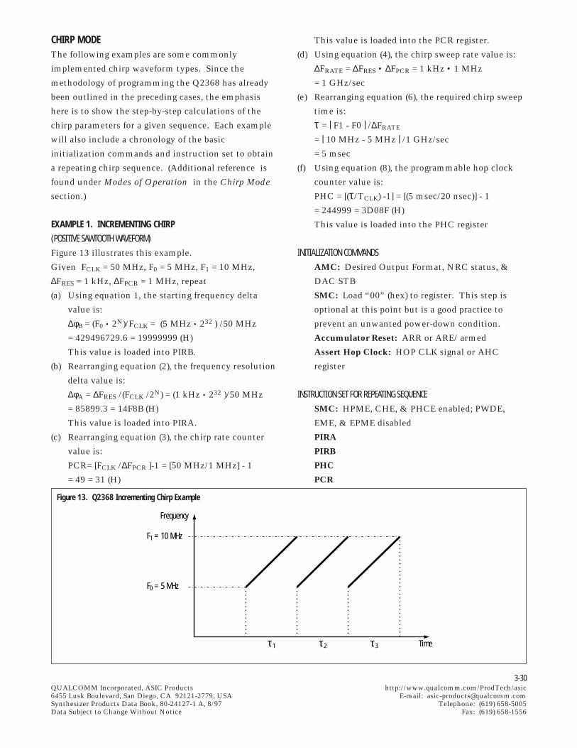
3-30QUALCOMM Incorporated, ASIC Products http://www.qualcomm.com/ProdTech/asic6455 Lusk Boulevard, San Diego, CA 92121-2779, USA E-mail: [email protected] Products Data Book, 80-24127-1 A, 8/97 Telephone: (619) 658-5005Data Subject to Change Without Notice Fax: (619) 658-1556
CHIRP MODEThe following examples are some commonly
implemented chirp waveform types. Since the
methodology of programming the Q2368 has already
been outlined in the preceding cases, the emphasis
here is to show the step-by-step calculations of the
chirp parameters for a given sequence. Each example
will also include a chronology of the basic
initialization commands and instruction set to obtain
a repeating chirp sequence. (Additional reference is
found under Modes of Operation in the Chirp Mode
section.)
EXAMPLE 1. INCREMENTING CHIRP(POSITIVE SAWTOOTH WAVEFORM)
Figure 13 illustrates this example.
Given FCLK = 50 MHz, F0 = 5 MHz, F1 = 10 MHz,
∆FRES = 1 kHz, ∆FPCR = 1 MHz, repeat
(a) Using equation 1, the starting frequency delta
value is:
∆φB = (F0 • 2N)/FCLK = (5 MHz • 232 ) /50 MHz
= 429496729.6 = 19999999 (H)
This value is loaded into PIRB.
(b) Rearranging equation (2), the frequency resolution
delta value is:
∆φA = ∆FRES /(FCLK /2N) = (1 kHz • 232 )/50 MHz
= 85899.3 = 14F8B (H)
This value is loaded into PIRA.
(c) Rearranging equation (3), the chirp rate counter
value is:
PCR= [FCLK /∆FPCR ]-1 = [50 MHz/1 MHz] - 1
= 49 = 31 (H)
This value is loaded into the PCR register.
(d) Using equation (4), the chirp sweep rate value is:
∆FRATE = ∆FRES • ∆FPCR = 1 kHz • 1 MHz
= 1 GHz/sec
(e) Rearranging equation (6), the required chirp sweep
time is:
τ = | F1 - F0 | /∆FRATE
= | 10 MHz - 5 MHz | /1 GHz/sec
= 5 msec
(f) Using equation (8), the programmable hop clock
counter value is:
PHC = [(τ/TCLK) -1] = [(5 msec/20 nsec)] - 1
= 244999 = 3D08F (H)
This value is loaded into the PHC register
INITIALIZATION COMMANDS
AMC: Desired Output Format, NRC status, &
DAC STB
SMC: Load “00” (hex) to register. This step is
optional at this point but is a good practice to
prevent an unwanted power-down condition.
Accumulator Reset: ARR or ARE/ armed
Assert Hop Clock: HOP CLK signal or AHC
register
INSTRUCTION SET FOR REPEATING SEQUENCE
SMC: HPME, CHE, & PHCE enabled; PWDE,
EME, & EPME disabled
PIRA
PIRB
PHC
PCR
F0 = 5 MHz
Frequency
F1 = 10 MHz
τ1 τ2 τ3 Time
Figure 13. Q2368 Incrementing Chirp Example
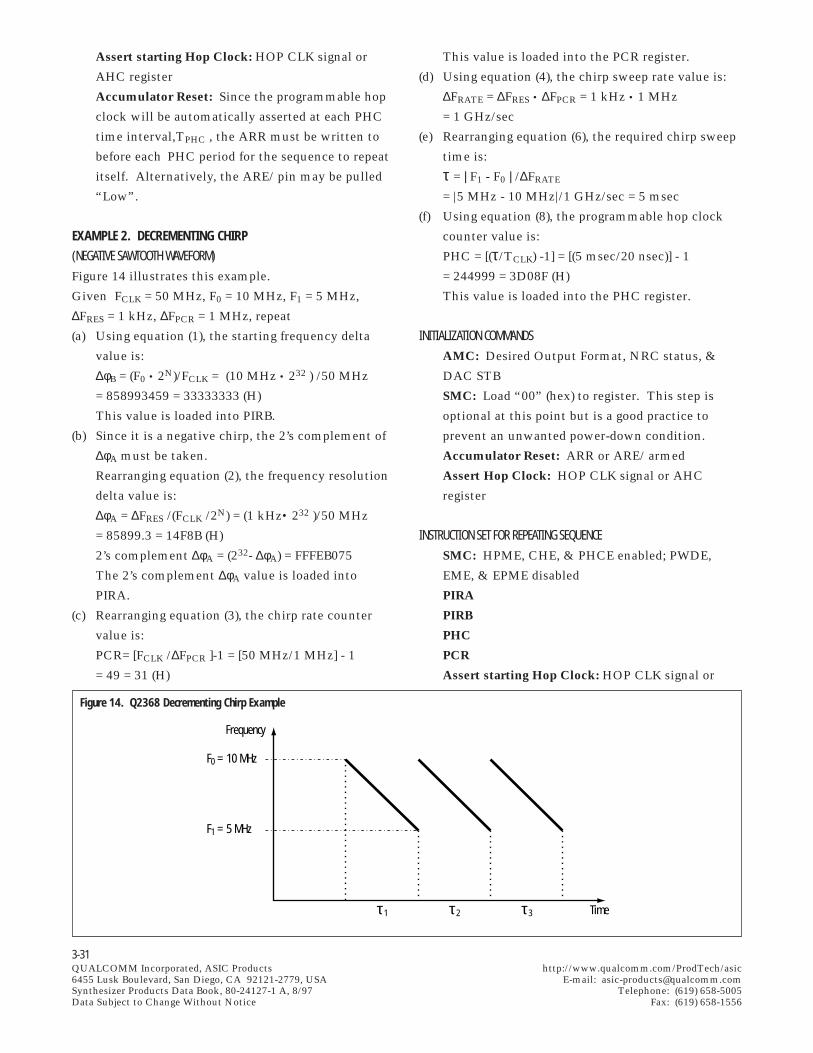
3-31QUALCOMM Incorporated, ASIC Products http://www.qualcomm.com/ProdTech/asic6455 Lusk Boulevard, San Diego, CA 92121-2779, USA E-mail: [email protected] Products Data Book, 80-24127-1 A, 8/97 Telephone: (619) 658-5005Data Subject to Change Without Notice Fax: (619) 658-1556
Assert starting Hop Clock: HOP CLK signal or
AHC register
Accumulator Reset: Since the programmable hop
clock will be automatically asserted at each PHC
time interval,TPHC , the ARR must be written to
before each PHC period for the sequence to repeat
itself. Alternatively, the ARE/ pin may be pulled
“Low”.
EXAMPLE 2. DECREMENTING CHIRP(NEGATIVE SAWTOOTH WAVEFORM)
Figure 14 illustrates this example.
Given FCLK = 50 MHz, F0 = 10 MHz, F1 = 5 MHz,
∆FRES = 1 kHz, ∆FPCR = 1 MHz, repeat
(a) Using equation (1), the starting frequency delta
value is:
∆φB = (F0 • 2N)/FCLK = (10 MHz • 232 ) /50 MHz
= 858993459 = 33333333 (H)
This value is loaded into PIRB.
(b) Since it is a negative chirp, the 2’s complement of
∆φA must be taken.
Rearranging equation (2), the frequency resolution
delta value is:
∆φA = ∆FRES /(FCLK /2N) = (1 kHz• 232 )/50 MHz
= 85899.3 = 14F8B (H)
2’s complement ∆φA = (232- ∆φA) = FFFEB075
The 2’s complement ∆φA value is loaded into
PIRA.
(c) Rearranging equation (3), the chirp rate counter
value is:
PCR= [FCLK /∆FPCR ]-1 = [50 MHz/1 MHz] - 1
= 49 = 31 (H)
This value is loaded into the PCR register.
(d) Using equation (4), the chirp sweep rate value is:
∆FRATE = ∆FRES • ∆FPCR = 1 kHz • 1 MHz
= 1 GHz/sec
(e) Rearranging equation (6), the required chirp sweep
time is:
τ = | F1 - F0 | /∆FRATE
= |5 MHz - 10 MHz|/1 GHz/sec = 5 msec
(f) Using equation (8), the programmable hop clock
counter value is:
PHC = [(τ/TCLK) -1] = [(5 msec/20 nsec)] - 1
= 244999 = 3D08F (H)
This value is loaded into the PHC register.
INITIALIZATION COMMANDS
AMC: Desired Output Format, NRC status, &
DAC STB
SMC: Load “00” (hex) to register. This step is
optional at this point but is a good practice to
prevent an unwanted power-down condition.
Accumulator Reset: ARR or ARE/ armed
Assert Hop Clock: HOP CLK signal or AHC
register
INSTRUCTION SET FOR REPEATING SEQUENCE
SMC: HPME, CHE, & PHCE enabled; PWDE,
EME, & EPME disabled
PIRA
PIRB
PHC
PCR
Assert starting Hop Clock: HOP CLK signal or
F1 = 5 MHz
Frequency
F0 = 10 MHz
τ1 τ2 τ3 Time
Figure 14. Q2368 Decrementing Chirp Example
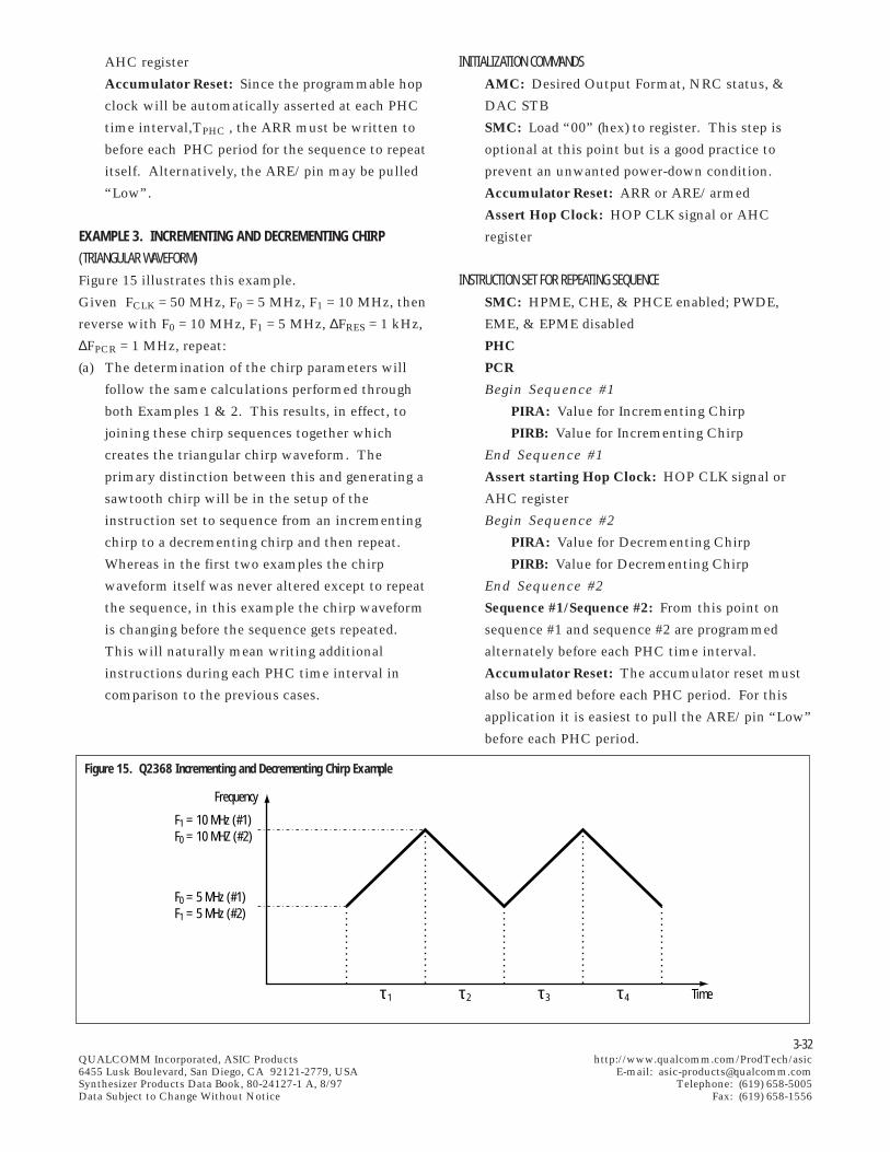
3-32QUALCOMM Incorporated, ASIC Products http://www.qualcomm.com/ProdTech/asic6455 Lusk Boulevard, San Diego, CA 92121-2779, USA E-mail: [email protected] Products Data Book, 80-24127-1 A, 8/97 Telephone: (619) 658-5005Data Subject to Change Without Notice Fax: (619) 658-1556
AHC register
Accumulator Reset: Since the programmable hop
clock will be automatically asserted at each PHC
time interval,TPHC , the ARR must be written to
before each PHC period for the sequence to repeat
itself. Alternatively, the ARE/ pin may be pulled
“Low”.
EXAMPLE 3. INCREMENTING AND DECREMENTING CHIRP(TRIANGULAR WAVEFORM)
Figure 15 illustrates this example.
Given FCLK = 50 MHz, F0 = 5 MHz, F1 = 10 MHz, then
reverse with F0 = 10 MHz, F1 = 5 MHz, ∆FRES = 1 kHz,
∆FPCR = 1 MHz, repeat:
(a) The determination of the chirp parameters will
follow the same calculations performed through
both Examples 1 & 2. This results, in effect, to
joining these chirp sequences together which
creates the triangular chirp waveform. The
primary distinction between this and generating a
sawtooth chirp will be in the setup of the
instruction set to sequence from an incrementing
chirp to a decrementing chirp and then repeat.
Whereas in the first two examples the chirp
waveform itself was never altered except to repeat
the sequence, in this example the chirp waveform
is changing before the sequence gets repeated.
This will naturally mean writing additional
instructions during each PHC time interval in
comparison to the previous cases.
INITIALIZATION COMMANDS
AMC: Desired Output Format, NRC status, &
DAC STB
SMC: Load “00” (hex) to register. This step is
optional at this point but is a good practice to
prevent an unwanted power-down condition.
Accumulator Reset: ARR or ARE/ armed
Assert Hop Clock: HOP CLK signal or AHC
register
INSTRUCTION SET FOR REPEATING SEQUENCE
SMC: HPME, CHE, & PHCE enabled; PWDE,
EME, & EPME disabled
PHC
PCR
Begin Sequence #1
PIRA: Value for Incrementing Chirp
PIRB: Value for Incrementing Chirp
End Sequence #1
Assert starting Hop Clock: HOP CLK signal or
AHC register
Begin Sequence #2
PIRA: Value for Decrementing Chirp
PIRB: Value for Decrementing Chirp
End Sequence #2
Sequence #1/Sequence #2: From this point on
sequence #1 and sequence #2 are programmed
alternately before each PHC time interval.
Accumulator Reset: The accumulator reset must
also be armed before each PHC period. For this
application it is easiest to pull the ARE/ pin “Low”
before each PHC period.
F0 = 5 MHz (#1)F1 = 5 MHz (#2)
Frequency
F1 = 10 MHz (#1)F0 = 10 MHZ (#2)
τ1 τ2 τ3 τ4 Time
Figure 15. Q2368 Incrementing and Decrementing Chirp Example
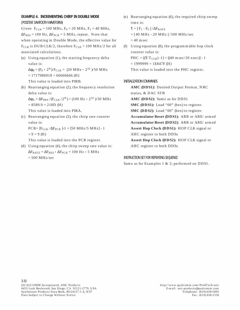
3-33QUALCOMM Incorporated, ASIC Products http://www.qualcomm.com/ProdTech/asic6455 Lusk Boulevard, San Diego, CA 92121-2779, USA E-mail: [email protected] Products Data Book, 80-24127-1 A, 8/97 Telephone: (619) 658-5005Data Subject to Change Without Notice Fax: (619) 658-1556
EXAMPLE 4. INCREMENTING CHIRP IN DOUBLE MODE(POSITIVE SAWTOOTH WAVEFORM)
Given FCLK = 100 MHz, F0 = 20 MHz, F1 = 40 MHz,
∆FRES = 100 Hz, ∆FPCR = 5 MHz, repeat. Note that
when operating in Double Mode, the effective value for
FCLK is DUB CLK/2, therefore FCLK = 100 MHz/2 for all
associated calculations.
(a) Using equation (1), the starting frequency delta
value is:
∆φB = (F0 • 2N)/FCLK = (20 MHz • 232 )/50 MHz
= 1717986918 = 66666666 (H)
This value is loaded into PIRB.
(b) Rearranging equation (2), the frequency resolution
delta value is:
∆φA = ∆FRES /(FCLK /2N) = (100 Hz • 232 )/50 MHz
= 8589.9 = 218D (H)
This value is loaded into PIRA.
(c) Rearranging equation (3), the chirp rate counter
value is:
PCR= [FCLK /∆FPCR ]-1 = [50 MHz/5 MHz] - 1
= 9 = 9 (H)
This value is loaded into the PCR register.
(d) Using equation (4), the chirp sweep rate value is:
∆FRATE = ∆FRES • ∆FPCR = 100 Hz • 5 MHz
= 500 MHz/sec
(e) Rearranging equation (6), the required chirp sweep
time is:
τ = | F1 - F0 | /∆FRATE
= | 40 MHz - 20 MHz | /500 MHz/sec
= 40 msec
(f) Using equation (8), the programmable hop clock
counter value is:
PHC = [(τ/TCLK) -1] = [(40 msec/20 nsec)] - 1
= 1999999 = 1E847F (H)
This value is loaded into the PHC register.
INITIALIZATION COMMANDS
AMC (DDS1): Desired Output Format, NRC
status, & DAC STB
AMC (DDS2): Same as for DDS1
SMC (DDS1): Load “00” (hex) to register.
SMC (DDS2): Load “00” (hex) to register.
Accumulator Reset (DDS1): ARR or ARE/ armed
Accumulator Reset (DDS2): ARR or ARE/ armed
Assert Hop Clock (DDS1): HOP CLK signal or
AHC register to both DDSs
Assert Hop Clock (DDS2): HOP CLK signal or
AHC register to both DDSs
INSTRUCTION SET FOR REPEATING SEQUENCE
Same as for Examples 1 & 2; performed on DDS1.
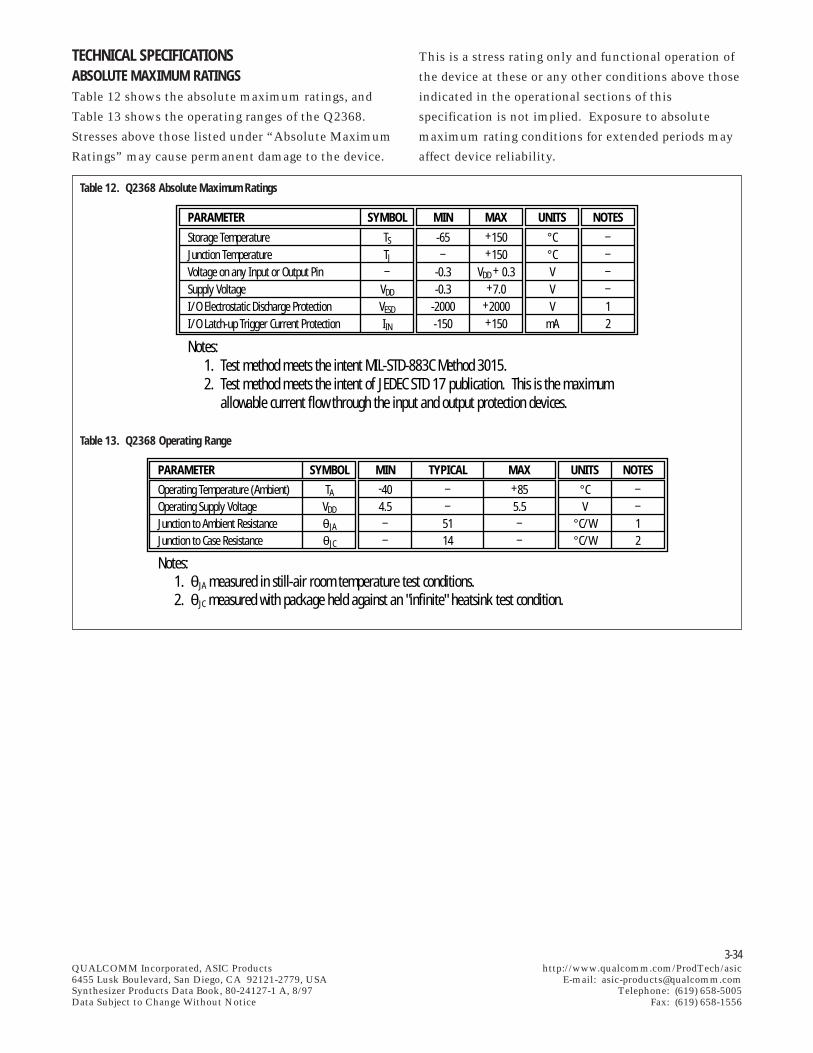
3-34QUALCOMM Incorporated, ASIC Products http://www.qualcomm.com/ProdTech/asic6455 Lusk Boulevard, San Diego, CA 92121-2779, USA E-mail: [email protected] Products Data Book, 80-24127-1 A, 8/97 Telephone: (619) 658-5005Data Subject to Change Without Notice Fax: (619) 658-1556
TECHNICAL SPECIFICATIONSABSOLUTE MAXIMUM RATINGSTable 12 shows the absolute maximum ratings, and
Table 13 shows the operating ranges of the Q2368.
Stresses above those listed under “Absolute Maximum
Ratings” may cause permanent damage to the device.
PARAMETER
Storage TemperatureJunction TemperatureVoltage on any Input or Output PinSupply VoltageI/O Electrostatic Discharge ProtectionI/O Latch-up Trigger Current Protection
Notes: 1. Test method meets the intent MIL-STD-883C Method 3015. 2. Test method meets the intent of JEDEC STD 17 publication. This is the maximum allowable current flow through the input and output protection devices.
SYMBOL
TS
TJ
–VDD
VESD
IIN
MIN
-65–
-0.3-0.3
-2000-150
MAX+150+150
VDD + 0.3+7.0
+2000+150
UNITS
°C°CVVV
mA
NOTES––––12
Table 12. Q2368 Absolute Maximum Ratings
Table 13. Q2368 Operating Range
PARAMETER
Operating Temperature (Ambient)Operating Supply Voltage Junction to Ambient ResistanceJunction to Case Resistance
Notes: 1. θJA measured in still-air room temperature test conditions. 2. θJC measured with package held against an "infinite" heatsink test condition.
SYMBOL
TA
VDD
θJA
θJC
MIN-404.5––
TYPICAL––5114
MAX+855.5––
UNITS
°CV
°C/W°C/W
NOTES––12
This is a stress rating only and functional operation of
the device at these or any other conditions above those
indicated in the operational sections of this
specification is not implied. Exposure to absolute
maximum rating conditions for extended periods may
affect device reliability.
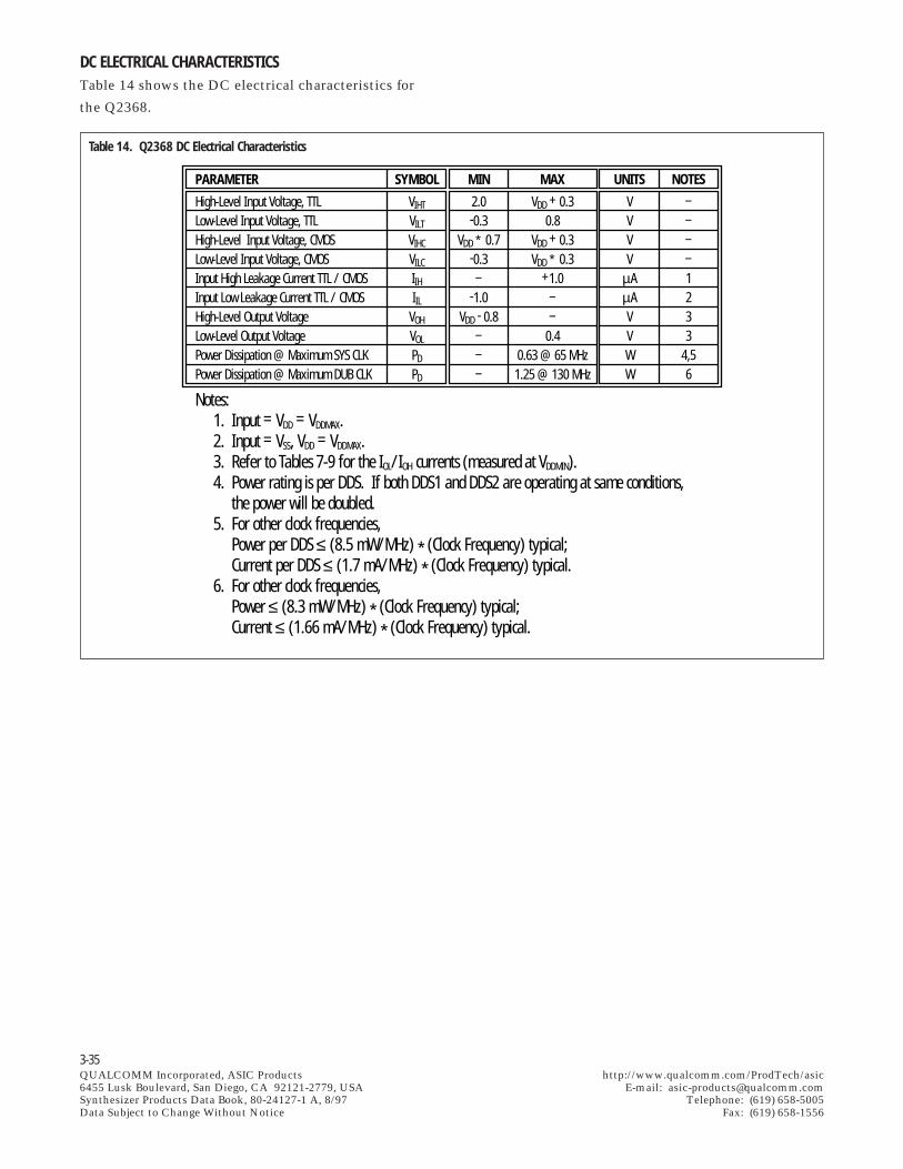
3-35QUALCOMM Incorporated, ASIC Products http://www.qualcomm.com/ProdTech/asic6455 Lusk Boulevard, San Diego, CA 92121-2779, USA E-mail: [email protected] Products Data Book, 80-24127-1 A, 8/97 Telephone: (619) 658-5005Data Subject to Change Without Notice Fax: (619) 658-1556
DC ELECTRICAL CHARACTERISTICSTable 14 shows the DC electrical characteristics for
the Q2368.
Table 14. Q2368 DC Electrical Characteristics
PARAMETER
High-Level Input Voltage, TTLLow-Level Input Voltage, TTLHigh-Level Input Voltage, CMOSLow-Level Input Voltage, CMOSInput High Leakage Current TTL / CMOSInput Low Leakage Current TTL / CMOSHigh-Level Output VoltageLow-Level Output VoltagePower Dissipation @ Maximum SYS CLKPower Dissipation @ Maximum DUB CLK
Notes: 1. Input = VDD = VDDMAX. 2. Input = VSS, VDD = VDDMAX. 3. Refer to Tables 7-9 for the IOL/IOH currents (measured at VDDMIN). 4. Power rating is per DDS. If both DDS1 and DDS2 are operating at same conditions, the power will be doubled. 5. For other clock frequencies, Power per DDS ≤ (8.5 mW/MHz) * (Clock Frequency) typical; Current per DDS ≤ (1.7 mA/MHz) * (Clock Frequency) typical. 6. For other clock frequencies, Power ≤ (8.3 mW/MHz) * (Clock Frequency) typical; Current ≤ (1.66 mA/MHz) * (Clock Frequency) typical.
SYMBOL
VIHT
VILT
VIHC
VILC
IIHIIL
VOH
VOL
PD
PD
MIN
2.0-0.3
VDD ∗ 0.7-0.3–
-1.0VDD - 0.8
–––
MAX
VDD + 0.30.8
VDD + 0.3VDD ∗ 0.3
+1.0––
0.40.63 @ 65 MHz
1.25 @ 130 MHz
UNITS
VVVV
µAµAVVWW
NOTES––––1233
4,56
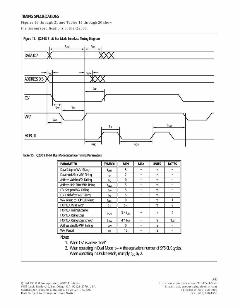
3-36QUALCOMM Incorporated, ASIC Products http://www.qualcomm.com/ProdTech/asic6455 Lusk Boulevard, San Diego, CA 92121-2779, USA E-mail: [email protected] Products Data Book, 80-24127-1 A, 8/97 Telephone: (619) 658-5005Data Subject to Change Without Notice Fax: (619) 658-1556
TIMING SPECIFICATIONSFigures 16 through 21 and Tables 15 through 20 show
the timing specifications of the Q2368.
Figure 16. Q2368 8-bit Bus Mode Interface Timing Diagram
DATA 0:7
ADDRESS 0:5
CS/
WR/
HOPCLK
tDSU tDH
tAC tWAX
tWC
tCW tWR
tAW
tHC
tWHC tHCHC
tHCW
Table 15. Q2368 8-bit Bus Mode Interface Timing Parameters
PARAMETER
Data Setup to WR/ RisingData Hold After WR/ RisingAddress Valid to CS/ FallingAddress Hold After WR/ RisingCS/ Setup to WR/ FallingCS/ Hold After WR/ RisingWR/ Rising to HOP CLK RisingHOP CLK Pulse WidthHOP CLK Falling Edge toHOP CLK Rising EdgeHOP CLK Rising Edge to WR/Address Valid to WR/ FallingWR/ Period
Notes: 1. When CS/ is active "Low". 2. When operating in Dual Mode, tCYC = the equivalent number of SYS CLK cycles. When operating in Double Mode, multiply tCYC by 2.
SYMBOL
tDSU
tDH
tAC
tWAX
tCW
tWC
tWHC
tHC
tHCHC
tHCW
tAW
tWR
MIN
5205550
tCYC
3 ∗ tCYC
4 ∗ tCYC
016
MAX––––––––
–
–––
UNITS
nsnsnsnsnsnsnsns
ns
nsnsns
NOTES––––––12
2
1,2––
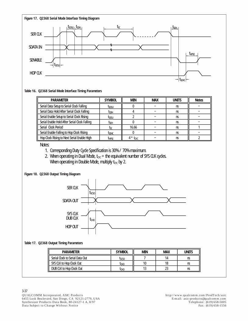
3-37QUALCOMM Incorporated, ASIC Products http://www.qualcomm.com/ProdTech/asic6455 Lusk Boulevard, San Diego, CA 92121-2779, USA E-mail: [email protected] Products Data Book, 80-24127-1 A, 8/97 Telephone: (619) 658-5005Data Subject to Change Without Notice Fax: (619) 658-1556
Figure 17. Q2368 Serial Mode Interface Timing Diagram
tSEHtSDH tSCtSDSU
tSESU
SER CLK
SDATA IN
SENABLE
HOP CLKtSEHC
tHPSE
Table 16. Q2368 Serial Mode Interface Timing Parameters
PARAMETER
Serial Data Setup to Serial Clock FallingSerial Data Hold After Serial Clock FallingSerial Enable Setup to Serial Clock RisingSerial Enable Hold After Serial Clock FallingSerial Clock PeriodSerial Enable Falling to Hop Clock RisingHop Clock Rising to Next Serial Enable High
Notes: 1. Corresponding Duty Cycle Specification is 30% / 70% maximum. 2. When operating in Dual Mode, tCYC = the equivalent number of SYS CLK cycles. When operating in Double Mode, multiply tCYC by 2.
SYMBOL
tSDSU
tSDH
tSESU
tSEH
tSC
tSEHC
tHPSE
MIN
0420
16.660
4 ∗ tCYC
MAX–––––––
UNITS
nsnsnsnsnsnsns
Notes––––1–2
Figure 18. Q2368 Output Timing Diagram
tSCSO
SER CLK
SDATA OUT
SYS CLK
HOP OUT
tCHODUB CLK
Table 17. Q2368 Output Timing Parameters
PARAMETER
Serial Clock to Serial Data OutSYS CLK to Hop Clock OutDUB CLK to Hop Clock Out
SYMBOL
tSCSO
tCHO
tCHO
MIN
71013
MAX
141823
UNITS
nsnsns
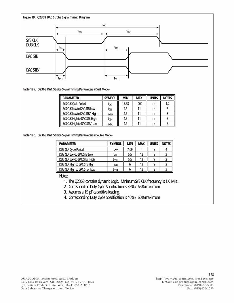
3-38QUALCOMM Incorporated, ASIC Products http://www.qualcomm.com/ProdTech/asic6455 Lusk Boulevard, San Diego, CA 92121-2779, USA E-mail: [email protected] Products Data Book, 80-24127-1 A, 8/97 Telephone: (619) 658-5005Data Subject to Change Without Notice Fax: (619) 658-1556
Figure 19. Q2368 DAC Strobe Signal Timing Diagram
tCYC
SYS CLKDUB CLK
DAC STB
DAC STB/
tCYCL tCYCH
tDSHtDSL
tDSLH tDSHL
Table 18a. Q2368 DAC Strobe Signal Timing Parameters (Dual Mode)
PARAMETER
SYS CLK Cycle PeriodSYS CLK Low to DAC STB LowSYS CLK Low to DAC STB/ HighSYS CLK High to DAC STB HighSYS CLK High to DAC STB/ Low
SYMBOL
tCYC
tDSL
tDSLH
tDSH
tDSHL
MIN
15.384.54.54.54.5
MAX
100011111111
UNITS
nsnsnsnsns
NOTES
1,23333
Table 18b. Q2368 DAC Strobe Signal Timing Parameters (Double Mode)
PARAMETER
DUB CLK Cycle PeriodDUB CLK Low to DAC STB LowDUB CLK Low to DAC STB/ HighDUB CLK High to DAC STB HighDUB CLK High to DAC STB/ Low
Notes: 1. The Q2368 contains dynamic Logic. Minimum SYS CLK frequency is 1.0 MHz. 2. Corresponding Duty Cycle Specification is 35% / 65% maximum. 3. Assumes a 15 pF capacitive loading. 4. Corresponding Duty Cycle Specification is 40% / 60% maximum.
SYMBOL
tCYC
tDSL
tDSLH
tDSH
tDSHL
MIN
7.695.55.566
MAX–
12121212
UNITS
nsnsnsnsns
NOTES
43333
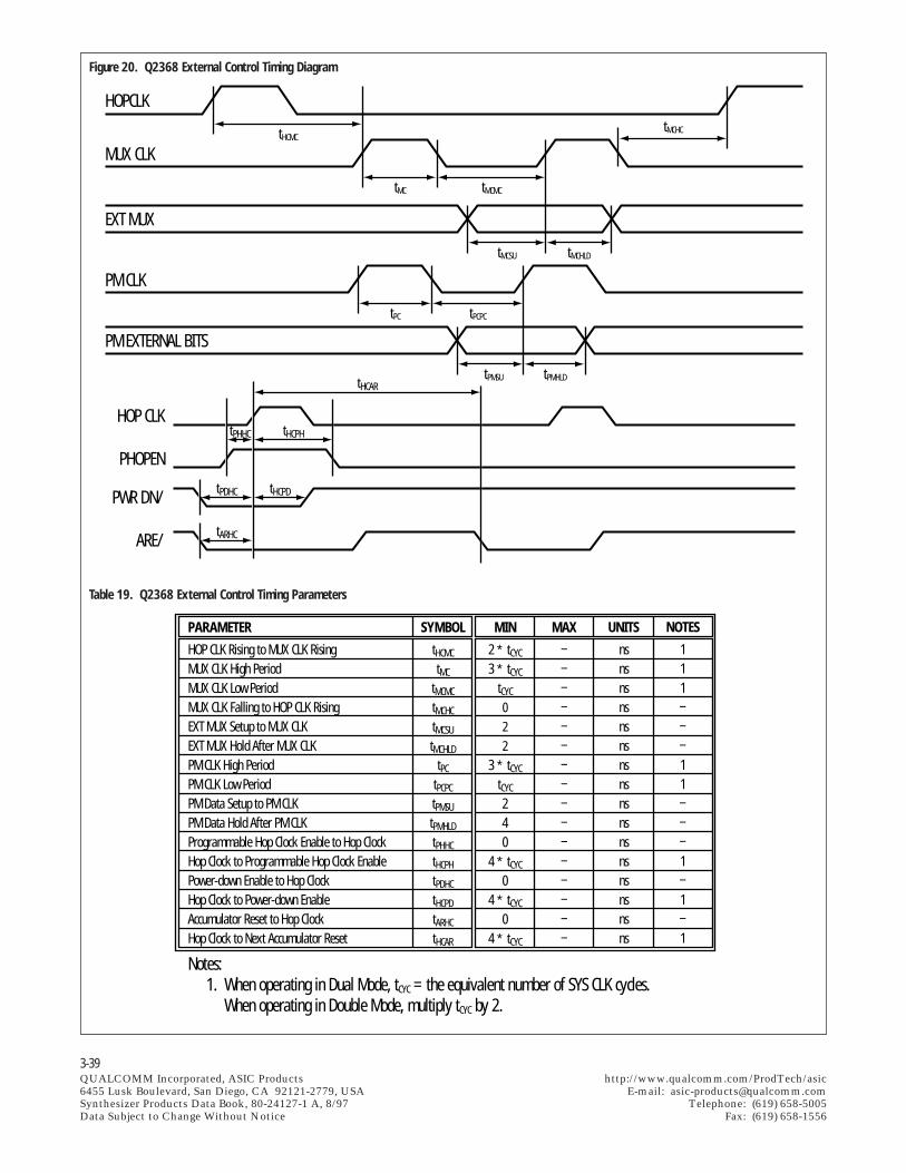
3-39QUALCOMM Incorporated, ASIC Products http://www.qualcomm.com/ProdTech/asic6455 Lusk Boulevard, San Diego, CA 92121-2779, USA E-mail: [email protected] Products Data Book, 80-24127-1 A, 8/97 Telephone: (619) 658-5005Data Subject to Change Without Notice Fax: (619) 658-1556
Figure 20. Q2368 External Control Timing Diagram
HOPCLK
MUX CLK
EXT MUX
PM CLK
PM EXTERNAL BITS
tHCMC
tMC tMCMC
tMCHC
tMCSU tMCHLD
tPC tPCPC
tPMSU tPMHLD
tPHHC tHCPH
tHCAR
tARHC
HOP CLK
PHOPEN
PWR DN/
ARE/
tPDHC tHCPD
Table 19. Q2368 External Control Timing Parameters
PARAMETER
HOP CLK Rising to MUX CLK RisingMUX CLK High PeriodMUX CLK Low PeriodMUX CLK Falling to HOP CLK RisingEXT MUX Setup to MUX CLKEXT MUX Hold After MUX CLKPM CLK High PeriodPM CLK Low PeriodPM Data Setup to PM CLKPM Data Hold After PM CLKProgrammable Hop Clock Enable to Hop ClockHop Clock to Programmable Hop Clock EnablePower-down Enable to Hop ClockHop Clock to Power-down EnableAccumulator Reset to Hop ClockHop Clock to Next Accumulator Reset
Notes: 1. When operating in Dual Mode, tCYC = the equivalent number of SYS CLK cycles. When operating in Double Mode, multiply tCYC by 2.
SYMBOL
tHCMC
tMC
tMCMC
tMCHC
tMCSU
tMCHLD
tPC
tPCPC
tPMSU
tPMHLD
tPHHC
tHCPH
tPDHC
tHCPD
tARHC
tHCAR
MIN
2 ∗ tCYC
3 ∗ tCYC
tCYC
022
3 ∗ tCYC
tCYC
240
4 ∗ tCYC
04 ∗ tCYC
04 ∗ tCYC
MAX––––––––––––––––
UNITS
nsnsnsnsnsnsnsnsnsnsnsnsnsnsnsns
NOTES
111–––11–––1–1–1
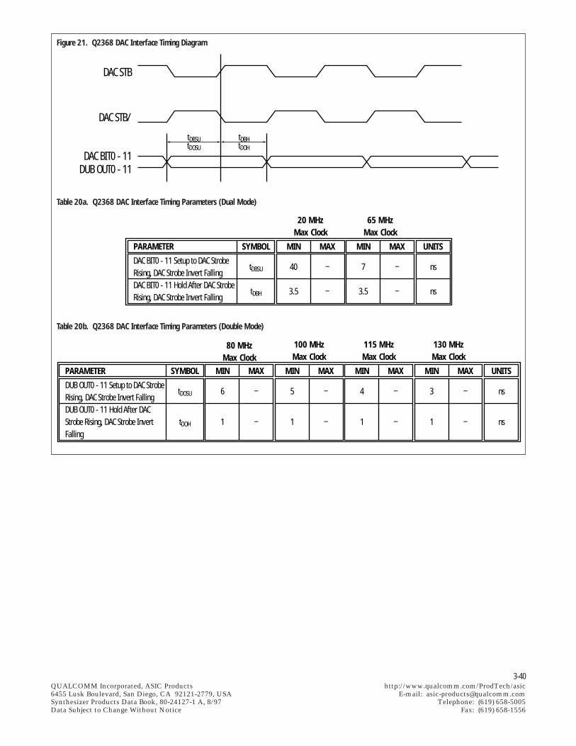
3-40QUALCOMM Incorporated, ASIC Products http://www.qualcomm.com/ProdTech/asic6455 Lusk Boulevard, San Diego, CA 92121-2779, USA E-mail: [email protected] Products Data Book, 80-24127-1 A, 8/97 Telephone: (619) 658-5005Data Subject to Change Without Notice Fax: (619) 658-1556
tDBSU tDBHtDOSU tDOH
DAC STB
DAC STB/
DAC BIT0 - 11DUB OUT0 - 11
Figure 21. Q2368 DAC Interface Timing Diagram
Table 20a. Q2368 DAC Interface Timing Parameters (Dual Mode)
PARAMETER
DAC BIT0 - 11 Setup to DAC StrobeRising, DAC Strobe Invert FallingDAC BIT0 - 11 Hold After DAC StrobeRising, DAC Strobe Invert Falling
MIN
40
3.5
MAX
–
–
MAX
–
–
MIN
7
3.5
UNITS
ns
ns
20 MHzMax Clock
65 MHzMax Clock
SYMBOL
tDBSU
tDBH
Table 20b. Q2368 DAC Interface Timing Parameters (Double Mode)
PARAMETER
DUB OUT0 - 11 Setup to DAC StrobeRising, DAC Strobe Invert FallingDUB OUT0 - 11 Hold After DACStrobe Rising, DAC Strobe InvertFalling
SYMBOL
tDOSU
tDOH
MIN
6
1
MAX
–
–
MAX
–
–
MIN
5
1
UNITS
ns
ns
80 MHzMax Clock
100 MHzMax Clock
MAX
–
–
MIN
4
1
115 MHzMax Clock
MAX
–
–
MIN
3
1
130 MHzMax Clock
3-41QUALCOMM Incorporated, ASIC Products http://www.qualcomm.com/ProdTech/asic6455 Lusk Boulevard, San Diego, CA 92121-2779, USA E-mail: [email protected] Products Data Book, 80-24127-1 A, 8/97 Telephone: (619) 658-5005Data Subject to Change Without Notice Fax: (619) 658-1556
0.667 (16.95)/0.687 (17.45) SQ.
0.541 (13.75)/0.561 (14.25) SQ.
Pin #1 Identifier100
1
25 51
75
26 50
76
5° TO 16° MAX
Detail B Detail A
0.139 (3.40) MAX0.019 (0.47)0.021 (0.53)
0.104 (2.55)0.124 (3.05)
0.010 (0.25) 0.027 (0.65)0.039 (0.95)
0.007 (0.17)0.011 (0.27)
0° TO 7° MAX
Detail A Detail B
All dimensions are ininches and (millimeters).
PQFP PACKAGINGThe Q2368 is packaged in a 100-pin Plastic Quad Flat
Pack (PQFP) shown in Figure 22.
Figure 22. Q2368 100-pin PQFP Package Outline
USING 3-WIRE EQUIVALENT SERIAL CONTROL FOR THEQ2368Although serial control for the Q2368 is accomplished
using four signals (SDATA IN, SER CLK, SENABLE
and HOP CLK), a 3-wire control method can be easily
implemented with the addition of a simple CMOS
Inverter as shown in Figure 23. Additional reference is
found under Digital Processor Interface Modes in the
Serial Bus Mode section and in the Serial Mode
Interface Timing information contained in Figure 17
and Table 16.
To SENABLEInput
74AC04
To HOP CLK Input
Figure 23. 3-wire Serial Control Implementation
3-42QUALCOMM Incorporated, ASIC Products http://www.qualcomm.com/ProdTech/asic6455 Lusk Boulevard, San Diego, CA 92121-2779, USA E-mail: [email protected] Products Data Book, 80-24127-1 A, 8/97 Telephone: (619) 658-5005Data Subject to Change Without Notice Fax: (619) 658-1556
PATENT REFERENCES1.) U.S. Patent No. 4,905,177 - “High Resolution
Phase to Sine Amplitude Conversion,”
QUALCOMM, Feb. 27, 1990.
2.) U.S. Patent No. 4,901,265 - “Pseudorandom
Dither for Frequency Synthesis Noise,”
QUALCOMM,
Feb. 13, 1990.
EVALUATION SYSTEM FOR THE Q2368 DDSThe Q0315 DDS Evaluation System was designed to
demonstrate the capabilities and operating modes of
the Q2368 dual DDS on a compact 5” X 7” printed
circuit board. The Q0315 contains several features
that will speed integration of the Q2368 into your
design. The evaluation platform allows customers to
evaluate the Q2368 as a dual DDS operating at 65
MHz or a single high-speed DDS operating at 130
MHz. A block diagram of the Q0315 Evaluation
System is shown in Figure 24.
The evaluation board contains a Q2368 device
coupled with a 125 MHz 10-bit Digital-to-Analog
Converter (DAC), a 100 MHz 12-bit DAC and the
necessary analog output circuitry to provide optimum
DDS performance.
The evaluation platform is computer controlled
through a digital I/O board that resides in the user’s
personal computer and Windows™ based software.
The menu driven Control Software provides access to
all Q2368 programmable registers and will
automatically compute all desired register values
based upon the user’s input and program the Q2368 in
the following modes:
• Dual Mode Control
• Double Mode Control
• Dual Mode Chirp Control
• Double Mode Chirp Control
• Register Mode
The User’s Guide provides all the information required
to operate the Q0315 and exercise all built-in
functionality of the Q2368. Appendices are also
provided which contain the schematics, layout and
complete parts list. The Q0315 consists of a DDS
Evaluation Board, Control Software, Control Cable,
Digital I/O (DIO) Board and DIO Board Installation
Software. In order to operate the DDS Evaluation
Board, the DIO Board needs to be installed in a PC.
The DIO Driver Software and the Q0315 Control
Software need to be installed on the hard drive of the
PC. The Q0315 DDS Evaluation System requires the
following computer hardware as a minimum to operate
in Remote Mode:
• PC 80386 or Better
• 4 MB RAM
• Math Co-processor
• Hard Drive
• Mouse
• Windows™ Version 3.1 or Windows ‘95™
• SVGA Video Card (1024 X 768 Resolution, Small
Fonts)
Note: Windows™ is a trademark of Microsoft ®
Corporation
3-43QUALCOMM Incorporated, ASIC Products http://www.qualcomm.com/ProdTech/asic6455 Lusk Boulevard, San Diego, CA 92121-2779, USA E-mail: [email protected] Products Data Book, 80-24127-1 A, 8/97 Telephone: (619) 658-5005Data Subject to Change Without Notice Fax: (619) 658-1556
Figure 24. Q0315 Evaluation System Block Diagram
HI573112 BitDAC
HI572110 BitDAC
50 MHzLow Pass
Filter
25 MHzLow Pass
Filter
Channel 2
Channel 1
PowerConditioning
Q2368DDS
DipSwitches
÷2
External Clock
125 MHz
SYS CLK1/SYS CLK2
DUB CLK
+5V -5V GND
+5VD
+5VA
-5VA
D GNDA GND
12
10
ComputerInterfaceConnector(DB37)
Q2368 ControlARE/PWRDN/PHOPENDUBENBUS_SEL
User InterfaceConnector(DIL 34) Default Path
Optional Path
AnalogOut
AnalogOut
4-1QUALCOMM Incorporated, ASIC Products http://www.qualcomm.com/ProdTech/asic6455 Lusk Boulevard, San Diego, CA 92121-2779, USA E-mail: [email protected] Products Data Book, 80-24127-1 A, 8/97 Telephone: (619) 658-5005Data Subject to Change Without Notice Fax: (619) 658-1556
Q2334DUAL DIRECT DIGITALSYNTHESIZER
APPLICATIONS• Spread Spectrum Modulators
• Quadrature Oscillators
• Programmable Frequency Synthesizers
• Satellite Receivers
• Cellular Base Stations
• Magnetic Resonance Imaging (MRI)
• VXI-based ATE
• SONAR/RADAR
• Paging Systems
• High Performance Test Equipment
• Digital Radios and Modems
• HF Transceivers
• Local Oscillator Generation for VSAT, DBS, and
GPS Applications
FEATURES• Two Complete Direct Digital Synthesizer
Functions On-chip
• Processor Interface for Control of Phase and
Frequency
• Patented Algorithmic Sine Lookup Function
• Patented Noise Reduction Circuit
• Synchronous PSK and FSK Modulation Inputs
• Phase Resolution: 0.00000008° Using Processor-
controlled Phase Adjustment
• Double Buffered Registers Allow Synchronous,
Phase Coherent Frequency Change
• Simple External Multiplex Control for Binary
Frequency Shift Keying (BFSK) Modulation
• Low Power: 667 mW Maximum at 50 MHz Clock
Frequency per DDS
• Evaluation Board Available: Q0310
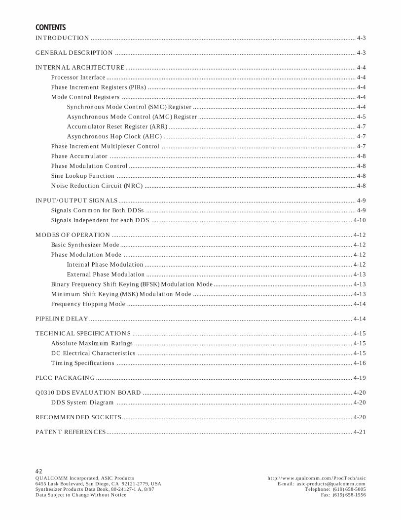
4-2QUALCOMM Incorporated, ASIC Products http://www.qualcomm.com/ProdTech/asic6455 Lusk Boulevard, San Diego, CA 92121-2779, USA E-mail: [email protected] Products Data Book, 80-24127-1 A, 8/97 Telephone: (619) 658-5005Data Subject to Change Without Notice Fax: (619) 658-1556
CONTENTSINTRODUCTION ......................................................................................................................................................... 4-3
GENERAL DESCRIPTION ........................................................................................................................................... 4-3
INTERNAL ARCHITECTURE ..................................................................................................................................... 4-4
Processor Interface ................................................................................................................................................ 4-4
Phase Increment Registers (PIRs) ........................................................................................................................ 4-4
Mode Control Registers ....................................................................................................................................... 4-4
Synchronous Mode Control (SMC) Register .............................................................................................. 4-4
Asynchronous Mode Control (AMC) Register ........................................................................................... 4-5
Accumulator Reset Register (ARR) ............................................................................................................ 4-7
Asynchronous Hop Clock (AHC) ............................................................................................................... 4-7
Phase Increment Multiplexer Control ................................................................................................................ 4-7
Phase Accumulator .............................................................................................................................................. 4-8
Phase Modulation Control ................................................................................................................................... 4-8
Sine Lookup Function .......................................................................................................................................... 4-8
Noise Reduction Circuit (NRC) .......................................................................................................................... 4-8
INPUT/OUTPUT SIGNALS ......................................................................................................................................... 4-9
Signals Common for Both DDSs ......................................................................................................................... 4-9
Signals Independent for each DDS .................................................................................................................... 4-10
MODES OF OPERATION........................................................................................................................................... 4-12
Basic Synthesizer Mode ...................................................................................................................................... 4-12
Phase Modulation Mode .................................................................................................................................... 4-12
Internal Phase Modulation........................................................................................................................ 4-12
External Phase Modulation ....................................................................................................................... 4-13
Binary Frequency Shift Keying (BFSK) Modulation Mode ................................................................................ 4-13
Minimum Shift Keying (MSK) Modulation Mode ............................................................................................ 4-13
Frequency Hopping Mode .................................................................................................................................. 4-14
PIPELINE DELAY ........................................................................................................................................................ 4-14
TECHNICAL SPECIFICATIONS ............................................................................................................................... 4-15
Absolute Maximum Ratings .............................................................................................................................. 4-15
DC Electrical Characteristics ............................................................................................................................ 4-15
Timing Specifications ........................................................................................................................................ 4-16
PLCC PACKAGING.................................................................................................................................................... 4-19
Q0310 DDS EVALUATION BOARD ......................................................................................................................... 4-20
DDS System Diagram ........................................................................................................................................ 4-20
RECOMMENDED SOCKETS..................................................................................................................................... 4-20
PATENT REFERENCES.............................................................................................................................................. 4-21
4-3QUALCOMM Incorporated, ASIC Products http://www.qualcomm.com/ProdTech/asic6455 Lusk Boulevard, San Diego, CA 92121-2779, USA E-mail: [email protected] Products Data Book, 80-24127-1 A, 8/97 Telephone: (619) 658-5005Data Subject to Change Without Notice Fax: (619) 658-1556
INTRODUCTIONQUALCOMM's Q2334 Dual Direct Digital
Synthesizer (DDS) generates high resolution digitized
sine wave signals using phase accumulation
techniques combined with a patented on-chip sine
lookup and Noise Reduction Circuit (NRC). The
Q2334 contains two independent DDS functions
controlled from a single microprocessor interface.
This interface controls both the phase and the
frequency of the generated sine waves as well as the
device’s operating mode. Synchronous inputs are also
provided to allow for phase and frequency modulation.
The Q2334 provides greater than 76 dB rejection of
phase truncation spurs and 72 dB amplitude
quantization signal-to-noise ratio. This synthesizer is
ideally suited for applications requiring high resolution
sine wave generation, fast phase and frequency
switching, and excellent phase and frequency stability.
The two independent on-chip DDS functions
provide an efficient technique for implementation of
full-duplex systems, quadrature oscillators, and spread
spectrum systems.
GENERAL DESCRIPTIONThe Q2334 consists of two independent DDS
functions, each controlled by a common
microprocessor interface, as illustrated in Figure 1.
Each DDS contains the following:
• Two Phase Increment Registers (PIR), A and B
• External Multiplex (Phase Increment Register)
Control
• 32-Bit Wide Phase Accumulator
• 3-Bit External Phase Modulation Control
• Patented Sine Lookup Algorithm (see Patent
Reference 1)
• Patented Noise Reduction Circuit (NRC) (see
Patent Reference 2)
ProcessorInterface
HOP CLK 1 HOP CLK 2
ExternalMultiplex Control 1
ExternalMultiplex Control 2
SYS CLK 2
External PhaseModulation Control 2
External PhaseModulation Control 1
SYS CLK 1
(32 Bits) (32 Bits) (32 Bits) (32 Bits)
(32 Bits)
(16 Bits)
(16 Bits)
(12 Bits)
(12 Bits)
(3 Bits) (3 Bits)
(32 Bits)
(16 Bits)
(16 Bits)
(12 Bits)
(12 Bits)Digitized Sine WaveOutput 1
Digitized Sine WaveOutput 2
Frequency/ModeControl
PhaseIncrementRegister A
PhaseIncrementRegister A
PhaseIncrementRegister B
PhaseIncrementRegister B
PhaseAccumulator
1
PhaseAccumulator
2
PhaseModulationControl 2
PhaseModulationControl 1
SineLookup 1
SineLookup 2
NoiseReductionCircuit 2
NoiseReductionCircuit 1
DDS 1 DDS 2
Figure 1. Q2334 Dual DDS Block Diagram
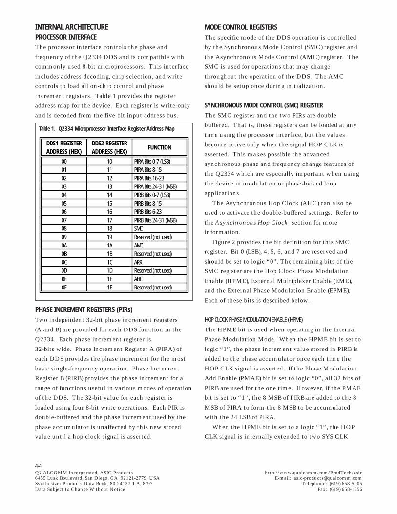
4-4QUALCOMM Incorporated, ASIC Products http://www.qualcomm.com/ProdTech/asic6455 Lusk Boulevard, San Diego, CA 92121-2779, USA E-mail: [email protected] Products Data Book, 80-24127-1 A, 8/97 Telephone: (619) 658-5005Data Subject to Change Without Notice Fax: (619) 658-1556
INTERNAL ARCHITECTUREPROCESSOR INTERFACEThe processor interface controls the phase and
frequency of the Q2334 DDS and is compatible with
commonly used 8-bit microprocessors. This interface
includes address decoding, chip selection, and write
controls to load all on-chip control and phase
increment registers. Table 1 provides the register
address map for the device. Each register is write-only
and is decoded from the five-bit input address bus.
MODE CONTROL REGISTERSThe specific mode of the DDS operation is controlled
by the Synchronous Mode Control (SMC) register and
the Asynchronous Mode Control (AMC) register. The
SMC is used for operations that may change
throughout the operation of the DDS. The AMC
should be setup once during initialization.
SYNCHRONOUS MODE CONTROL (SMC) REGISTERThe SMC register and the two PIRs are double
buffered. That is, these registers can be loaded at any
time using the processor interface, but the values
become active only when the signal HOP CLK is
asserted. This makes possible the advanced
synchronous phase and frequency change features of
the Q2334 which are especially important when using
the device in modulation or phase-locked loop
applications.
The Asynchronous Hop Clock (AHC) can also be
used to activate the double-buffered settings. Refer to
the Asynchronous Hop Clock section for more
information.
Figure 2 provides the bit definition for this SMC
register. Bit 0 (LSB), 4, 5, 6, and 7 are reserved and
should be set to logic “0”. The remaining bits of the
SMC register are the Hop Clock Phase Modulation
Enable (HPME), External Multiplexer Enable (EME),
and the External Phase Modulation Enable (EPME).
Each of these bits is described below.
HOP CLOCK PHASE MODULATION ENABLE (HPME)
The HPME bit is used when operating in the Internal
Phase Modulation Mode. When the HPME bit is set to
logic “1”, the phase increment value stored in PIRB is
added to the phase accumulator once each time the
HOP CLK signal is asserted. If the Phase Modulation
Add Enable (PMAE) bit is set to logic “0”, all 32 bits of
PIRB are used for the one time. However, if the PMAE
bit is set to “1”, the 8 MSB of PIRB are added to the 8
MSB of PIRA to form the 8 MSB to be accumulated
with the 24 LSB of PIRA.
When the HPME bit is set to a logic “1”, the HOP
CLK signal is internally extended to two SYS CLK
Table 1. Q2334 Microprocessor Interface Register Address Map
DDS1 REGISTERADDRESS (HEX)
000102030405060708090A0B0C0D0E0F
DDS2 REGISTERADDRESS (HEX)
101112131415161718191A1B1C1D1E1F
FUNCTION
PIRA Bits 0-7 (LSB)PIRA Bits 8-15PIRA Bits 16-23PIRA Bits 24-31 (MSB)PIRB Bits 0-7 (LSB)PIRB Bits 8-15PIRB Bits 6-23PIRB Bits 24-31 (MSB)SMCReserved (not used)AMCReserved (not used)ARRReserved (not used)AHCReserved (not used)
PHASE INCREMENT REGISTERS (PIRs)Two independent 32-bit phase increment registers
(A and B) are provided for each DDS function in the
Q2334. Each phase increment register is
32-bits wide. Phase Increment Register A (PIRA) of
each DDS provides the phase increment for the most
basic single-frequency operation. Phase Increment
Register B (PIRB) provides the phase increment for a
range of functions useful in various modes of operation
of the DDS. The 32-bit value for each register is
loaded using four 8-bit write operations. Each PIR is
double-buffered and the phase increment used by the
phase accumulator is unaffected by this new stored
value until a hop clock signal is asserted.
4-5QUALCOMM Incorporated, ASIC Products http://www.qualcomm.com/ProdTech/asic6455 Lusk Boulevard, San Diego, CA 92121-2779, USA E-mail: [email protected] Products Data Book, 80-24127-1 A, 8/97 Telephone: (619) 658-5005Data Subject to Change Without Notice Fax: (619) 658-1556
cycles. The two SYS CLK cycles make it possible for
the phase accumulator to add the contents from PIRB
once, and then switch the process immediately back to
PIRA. To disable the Internal Phase Modulation Mode,
as is the case when you want to reconfigure operation
to the Basic Oscillator Mode for example, the HPME
bit is reset to “0”. The HOP CLK is required to
initiate this change and during the HPME's transition
from “1” to “0”, the HOP CLK is no longer internally
extended to two SYS CLK cycles and therefore the
accumulation process will still accumulate the
contents from PIRB. In order to switch the
accumulation process back to PIRA, re-load PIRA with
the intended frequency value, then assert another HOP
CLK. Asserting a successive HOP CLK without re-
loading PIRA will not switch the accumulation process
from PIRB to PIRA. If desired, the contents of PIRB
can be loaded with the same contents intended for
PIRA concurrently with the HPME bit being disabled
to “0”. If this is done, then when the HPME
transitions, the output will look as though only PIRA
is being accumulated, although the user will want to
make sure to re-load PIRA with the desired value and
assert another HOP CLK so the accumulation process
ends up on PIRA.
EXTERNAL MULTIPLEXER ENABLE (EME)
The EME bit enables the External Multiplex Control.
When this bit is set to logic “1”, the EXT MUX signal
determines whether the value stored in PIRA or PIRB
will be used for the phase accumulation process. The
selection on the EXT MUX signal is synchronously
activated on the rising edge of the MUX CLK signal
when the EME is set to logic “1”. If the EME bit is set
to logic “0”, then the External Multiplex Control is
disabled and the signal on EXT MUX is ignored. In
this case, the contents of PIRA will be used for the
accumulation process.
EXTERNAL PHASE MODULATION ENABLE (EPME)
The EPME enables the External Phase Modulation
function. When this bit is set to “1”, the PM EXT
BITS are read and the corresponding phase offset is
latched into the Q2334 each time the PM CLK is
asserted. If External Phase Modulation is not used, set
the EPME bit to “0”. (Refer to the External Phase
Modulation section.)
ASYNCHRONOUS MODE CONTROL (AMC) REGISTERThe AMC register has an active value once the
information has been written to it. This register does
not require a HOP CLK signal to become active. The
AMC register of each DDS function includes control
bits which should only be configured during
initialization of the Q2334. The AMC commands
should be activated before any other commands are
asserted to the DDS in order for all commands to be
received and processed properly. These control bits, as
shown in Figure 3, include the DAC strobe or DAC
strobe invert (DAC STB, DAC STB/), Phase
Modulation Add Enable (PMAE), Output Format, and
NRC Enable. Each of these is described below. Bits 4
and 6 of the AMC register are reserved and should be
set to “0”.
Figure 2. Q2334 Synchronous Mode Control (SMC) Register
0* 0* 0* 0*
HOP CLKPHASE MOD
ENABLE(HPME)
0*
D7 D6 D5 D4 D3 D2 D1 D0
EXTMUX
ENABLE(EME)
EXT PHASEMOD
ENABLE(EPME)
ADDRESS × 08 or 18 [hex]
* These bits must be set to 0.
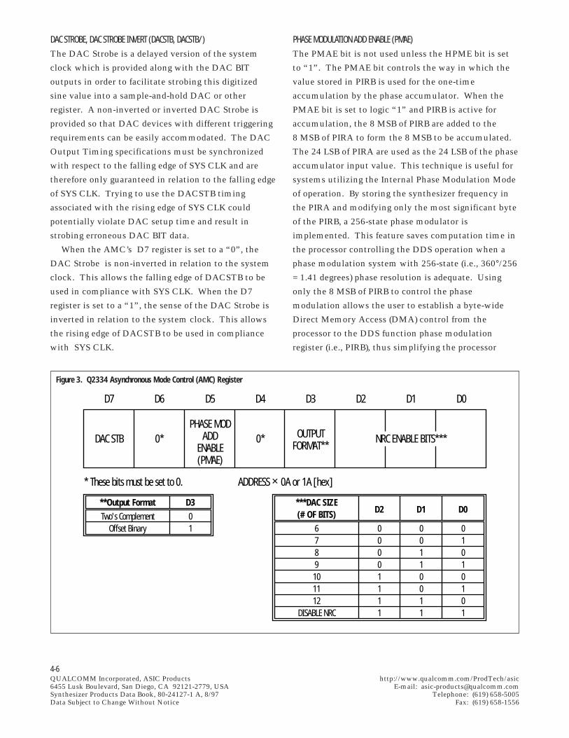
4-6QUALCOMM Incorporated, ASIC Products http://www.qualcomm.com/ProdTech/asic6455 Lusk Boulevard, San Diego, CA 92121-2779, USA E-mail: [email protected] Products Data Book, 80-24127-1 A, 8/97 Telephone: (619) 658-5005Data Subject to Change Without Notice Fax: (619) 658-1556
DAC STROBE, DAC STROBE INVERT (DACSTB, DACSTB/)
The DAC Strobe is a delayed version of the system
clock which is provided along with the DAC BIT
outputs in order to facilitate strobing this digitized
sine value into a sample-and-hold DAC or other
register. A non-inverted or inverted DAC Strobe is
provided so that DAC devices with different triggering
requirements can be easily accommodated. The DAC
Output Timing specifications must be synchronized
with respect to the falling edge of SYS CLK and are
therefore only guaranteed in relation to the falling edge
of SYS CLK. Trying to use the DACSTB timing
associated with the rising edge of SYS CLK could
potentially violate DAC setup time and result in
strobing erroneous DAC BIT data.
When the AMC’s D7 register is set to a “0”, the
DAC Strobe is non-inverted in relation to the system
clock. This allows the falling edge of DACSTB to be
used in compliance with SYS CLK. When the D7
register is set to a “1”, the sense of the DAC Strobe is
inverted in relation to the system clock. This allows
the rising edge of DACSTB to be used in compliance
with SYS CLK.
PHASE MODULATION ADD ENABLE (PMAE)
The PMAE bit is not used unless the HPME bit is set
to “1”. The PMAE bit controls the way in which the
value stored in PIRB is used for the one-time
accumulation by the phase accumulator. When the
PMAE bit is set to logic “1” and PIRB is active for
accumulation, the 8 MSB of PIRB are added to the
8 MSB of PIRA to form the 8 MSB to be accumulated.
The 24 LSB of PIRA are used as the 24 LSB of the phase
accumulator input value. This technique is useful for
systems utilizing the Internal Phase Modulation Mode
of operation. By storing the synthesizer frequency in
the PIRA and modifying only the most significant byte
of the PIRB, a 256-state phase modulator is
implemented. This feature saves computation time in
the processor controlling the DDS operation when a
phase modulation system with 256-state (i.e., 360°/256
= 1.41 degrees) phase resolution is adequate. Using
only the 8 MSB of PIRB to control the phase
modulation allows the user to establish a byte-wide
Direct Memory Access (DMA) control from the
processor to the DDS function phase modulation
register (i.e., PIRB), thus simplifying the processor
Figure 3. Q2334 Asynchronous Mode Control (AMC) Register
DAC STB 0* 0* OUTPUTFORMAT**
D7 D6 D5 D4 D3 D2 D1 D0
PHASE MODADD
ENABLE(PMAE)
ADDRESS × 0A or 1A [hex]* These bits must be set to 0.
NRC ENABLE BITS***
***DAC SIZE(# OF BITS)
6789
101112
DISABLE NRC
D2
00001111
D1
00110011
D0
01010101
**Output FormatTwo's Complement
Offset Binary
D301
4-7QUALCOMM Incorporated, ASIC Products http://www.qualcomm.com/ProdTech/asic6455 Lusk Boulevard, San Diego, CA 92121-2779, USA E-mail: [email protected] Products Data Book, 80-24127-1 A, 8/97 Telephone: (619) 658-5005Data Subject to Change Without Notice Fax: (619) 658-1556
overhead required to control the DDS function in
rapidly switching phase modulation systems. When
the PMAE bit is set to logic “0”, all 32-bits of PIRB
will be accumulated in the phase accumulator when
PIRB is active allowing a phase resolution of 360°/232,
i.e, 84 nano-degrees.
OUTPUT FORMAT
The Output Format bit determines the binary coding
of the DAC output bits of each DDS function. When
this bit is set to logic “1”, the DAC output is encoded
in offset binary format. When this bit is set to logic
“0”, the DAC output bits are encoded in two’s
complement format. Table 2 shows the effect of the
setting of the Output Format bit.
value to the ARR, the accumulator reset function is
armed. The next time the HOP CLK is asserted, the
phase accumulator is reset to zero.
ASYNCHRONOUS HOP CLOCK (AHC)Each DDS function includes an Asynchronous Hop
Clock (AHC) register. When any value is written to
this register, the previously stored values in the
double-buffered PIRA, PIRB, and SMC registers are
activated. This allows processor control of activation
of these settings in an identical fashion as with the
assertion of the HOP CLK signal. Note that the HOP
CLK signal must be “Low” when the AHC register is
accessed in order to activate the new register values.
Also note that the timing for the AHC is exactly the
same as the HOP CLK signal. Activation of the stored
settings occurs within four SYS CLK periods after
writing to the AHC register.
The AMC register has an active value once the
information has been written to it. This register does
not require a HOP CLK signal to become active.
PHASE INCREMENT MULTIPLEXER CONTROLThe phase increment multiplexer function selects
which PIR (A or B) is used for the accumulation
process. This multiplexing function provides a simple
Binary Frequency Shift Keying (BFSK) interface to the
DDS.
The signal EXT MUX controls the selection of the
value stored in either PIRA or PIRB. For EXT MUX
= 0, PIRA is selected; for EXT MUX = 1, PIRB is
selected. The signal MUX CLK enables the selection
made by the EXT MUX signal. The selection made by
the EXT MUX signal is activated synchronously once
during the low-to-high transition on the MUX CLK
signal.
The MUX CLK signal is internally synchronized to
the SYS CLK signal of the DDS. (Refer to the
Asynchronous Input information contained in
Figure 11 and Table 10.) The selection of the EXT
MUX control may occur as frequently as once every
four periods of SYS CLK. (Refer to the External
Control Timing information contained in Figure 10
and Table 9.)
VALUE
MAX Value………
Half MAX + 1Half MAX – 1
………
MIN Value
OUTPUT FORMAT = 1(OFFSET BINARY)
1 1 1 1 1 1 1 1 1 1 1 11 1 1 1 1 1 1 1 1 1 1 0
……
1 0 0 0 0 0 0 0 0 0 0 00 1 1 1 1 1 1 1 1 1 1 1
……
0 0 0 0 0 0 0 0 0 0 0 10 0 0 0 0 0 0 0 0 0 0 0
OUTPUT FORMAT = 0(TWO's COMPLEMENT)
0 1 1 1 1 1 1 1 1 1 1 10 1 1 1 1 1 1 1 1 1 1 0
……
0 0 0 0 0 0 0 0 0 0 0 01 1 1 1 1 1 1 1 1 1 1 1
……
1 0 0 0 0 0 0 0 0 0 0 11 0 0 0 0 0 0 0 0 0 0 0
LSBMSB LSBMSB
Table 2. Q2334 DAC Output Formats
NRC ENABLE
When using the on-chip Noise Reduction Circuit
(NRC) function, the number of significant bits to be
used from the DAC outputs must be programmed into
NRC Enable bits. The DAC bit-width is encoded in
three bits as shown in Figure 3. When using a DAC
with fewer than 12-bits resolution, the most
significant DAC output bits are valid. The NRC
function is disabled when the NRC Enable bits are set
to 111 (binary). The function of the NRC circuit is
described in the Noise Reduction Circuit section.
ACCUMULATOR RESET REGISTER (ARR)Each DDS function on the Q2334 includes an
Accumulator Reset Register (ARR). By writing any
4-8QUALCOMM Incorporated, ASIC Products http://www.qualcomm.com/ProdTech/asic6455 Lusk Boulevard, San Diego, CA 92121-2779, USA E-mail: [email protected] Products Data Book, 80-24127-1 A, 8/97 Telephone: (619) 658-5005Data Subject to Change Without Notice Fax: (619) 658-1556
PHASE ACCUMULATORTwo 32-bit wide phase accumulators are included in
the Q2334, one for each DDS function. These
accumulators compute and store the sum of the
previously computed phase value and the phase
increment value from either PIRA or PIRB once during
each period of SYS CLK.
PHASE MODULATION CONTROLUsing the external phase modulation inputs, PM EXT
BIT0-2, the output of the phase accumulator can be
offset by phase increments of 45 degrees (from 0
degrees to 315 degrees) without affecting the operation
of the phase accumulator. Table 3 shows the phase
offset for the possible settings of the 3-bit external
phase modulation inputs. These inputs are latched
into the DDS function when the signal PM CLK is
asserted. Changes in the external phase modulation
are synchronized internally to the DDS function. This
provides a simple 8-Phase Shift Keying (8PSK) interface
to the DDS.
Refer to the Modes of Operation section for more
detailed information on phase modulation.
SINE LOOKUP FUNCTIONThe Q2334 DDS implements a patented technique to
generate a sine wave lookup (see Patent Reference 1).
This algorithm takes the 16 MSB from the phase
accumulator to generate a 12-bit sine wave value.
Using this high precision lookup function, the phase
truncation noise of the sine wave output is kept below
76 dB. This technique differs considerably from the
traditional method of using a ROM lookup function.
This advanced look-up technique provides highly
accurate and precise sine wave generation.
NOISE REDUCTION CIRCUIT (NRC)Noise due to amplitude quantization is often assumed
to be random and uniformly distributed. However,
because a sine wave function is periodic, this is not
always the case. At certain output frequencies,
amplitude quantization errors become highly
correlated, thereby causing spurs.
Spurs associated with round-off errors of the
quantized sine wave outputs can be significantly
reduced by enabling the on-chip Noise Reduction
Circuit (NRC). This patented circuit distributes the
noise energy evenly across the frequency band, thus
reducing the amplitudes of peak spurious components
(see Patent Reference 2).
It is important to properly set the NRC Enable bits,
because the operation of the NRC is scaled to the LSB.
If an incorrectly sized DAC is specified, performance
will be reduced.
If the Q2334 is used to generate narrowband outputs
and a low noise floor is required, the signal should be
bandpass filtered and the NRC disabled. As stated
above, when the NRC is enabled it distributes the
noise evenly across the frequency band and raises the
noise floor. When the NRC is disabled, the noise floor
is slightly lower and the quantization errors show up
as discrete spurious. However, since the signal is
bandpass filtered, the broadband spurious will be
negligible.
The output of the NRC (a 12-bit wide digitized sine
wave) is normally connected to an external DAC
function. This output value can be encoded in offset
binary or two’s complement format (see Figure 3).
Figures 4 and 5 show typical spectra of the analog
converted outputs from the Q2334 with the NRC
enabled and disabled. These spectra were measured
with the DDS operating with a 10-bit DAC. The
synthesized frequency in each of these figures is 10.8
MHz from a 30 MHz system clock frequency. The
measurement frequency spans from 0 to 15 MHz, the
resolution bandwidth is 30 kHz, the video bandwidth
is 3 kHz, and the scale is 10 dB per vertical division.
Table 3. Q2334 External Phase Modulation Offset Settings
200001111
PM EXT BIT100110011
001010101
ABSOLUTE PHASEOFFSET (degrees)
04590
135180225270315
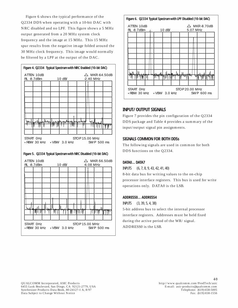
4-9QUALCOMM Incorporated, ASIC Products http://www.qualcomm.com/ProdTech/asic6455 Lusk Boulevard, San Diego, CA 92121-2779, USA E-mail: [email protected] Products Data Book, 80-24127-1 A, 8/97 Telephone: (619) 658-5005Data Subject to Change Without Notice Fax: (619) 658-1556
Figure 6 shows the typical performance of the
Q2334 DDS when operating with a 10-bit DAC with
NRC disabled and no LPF. This figure shows a 5 MHz
output generated from a 20 MHz system clock
frequency and the image at 15 MHz. This 15 MHz
spur results from the negative image folded around the
30 MHz clock frequency. This image would normally
be filtered by a LPF at the output of the DAC.
Figure 4. Q2334 Typical Spectrum with NRC Enabled (10-bit DAC)
ATTEN 10dBRL -8.7dBm 10 dB/
MKR -64.50dB-2.40 MHz
START 0Hz*RBW 30 kHz *VBW 3.0 kHz
STOP 15.00 MHzSWP 500 ms
Figure 5. Q2334 Typical Spectrum with NRC Disabled (10-bit DAC)
ATTEN 10dBRL -8.7dBm 10 dB/
MKR -56.50dB-6.08 MHz
START 0Hz*RBW 30 kHz *VBW 3.0 kHz
STOP 15.00 MHzSWP 500 ms
Figure 6. Q2334 Typical Spectrum with LPF Disabled (10-bit DAC)
ATTEN 10dBRL -8.7dBm 10 dB/
MKR -8.70dB5.07 MHz
START 0Hz*RBW 30 kHz *VBW 3.0 kHz
STOP 20.00 MHzSWP 600 ms
INPUT/OUTPUT SIGNALSFigure 7 provides the pin configuration of the Q2334
DDS package and Table 4 provides a summary of the
input/output signal pin assignments.
SIGNALS COMMON FOR BOTH DDSsThe following signals are used in common for both
DDS functions on the Q2334.
DATA0…DATA7INPUTS (6, 7, 8, 9, 43, 42, 41, 40)
8-bit data bus for writing values to the on-chip
processor interface registers. This bus is used for write
operations only. DATA0 is the LSB.
ADDRESS0…ADDRESS4INPUTS (3, 39, 5, 4, 38)
5-bit address bus to select the internal processor
interface registers. Addresses must be held fixed
during the active period of the WR/ signal.
ADDRESS0 is the LSB.
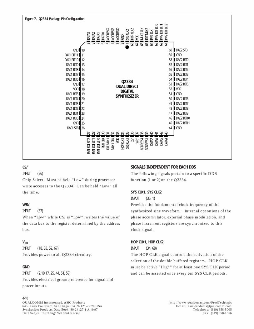
4-10QUALCOMM Incorporated, ASIC Products http://www.qualcomm.com/ProdTech/asic6455 Lusk Boulevard, San Diego, CA 92121-2779, USA E-mail: [email protected] Products Data Book, 80-24127-1 A, 8/97 Telephone: (619) 658-5005Data Subject to Change Without Notice Fax: (619) 658-1556
CS/INPUT (36)
Chip Select. Must be held “Low” during processor
write accesses to the Q2334. Can be held “Low” all
the time.
WR/INPUT (37)
When “Low” while CS/ is “Low”, writes the value of
the data bus to the register determined by the address
bus.
VDD
INPUT (18, 33, 52, 67)
Provides power to all Q2334 circuitry.
GNDINPUT (2,10,17, 25, 44, 51, 59)
Provides electrical ground reference for signal and
power inputs.
SIGNALS INDEPENDENT FOR EACH DDSThe following signals pertain to a specific DDS
function (1 or 2) on the Q2334.
SYS CLK1, SYS CLK2INPUT (35, 1)
Provides the fundamental clock frequency of the
synthesized sine waveform. Internal operations of the
phase accumulator, external phase modulation, and
phase increment registers are synchronized to this
clock signal.
HOP CLK1, HOP CLK2INPUT (34, 68)
The HOP CLK signal controls the activation of the
selection of the double buffered registers. HOP CLK
must be active “High” for at least one SYS CLK period
and can be asserted once every ten SYS CLK periods.
Figure 7. Q2334 Package Pin Configuration
6059585756555453525150494847464544
9 8 7 6 5 4 3 2 1 68 67 66 65 64 63 62 61
DAC2 STBGNDDAC2 BIT0DAC2 BIT1DAC2 BIT2DAC2 BIT3DAC2 BIT4DAC2 BIT5VDDGNDDAC2 BIT6DAC2 BIT7DAC2 BIT8DAC2 BIT9DAC2 BIT10DAC2 BIT11GND
GNDDAC1 BIT11DAC1 BIT10
DAC1 BIT9DAC1 BIT8DAC1 BIT7DAC1 BIT6
GNDVDD
DAC1 BIT5DAC1 BIT4DAC1 BIT3DAC1 BIT2DAC1 BIT1DAC1 BIT0
GNDDAC1 STB
1011121314151617181920212223242526
27 28 29 30 31 32 33 34 35 36 37 38 39 40 41 42 43
DATA
3DA
TA2
DATA
1DA
TA0
ADDR
ESS2
ADDR
ESS3
ADDR
ESS0
GND
SYS C
LK2
HOP
CLK2
VDD
MUX2
CLK
EXT M
UX2
PM2
CLK
PM2
EXT B
IT0PM
2 EX
T BIT1
PM2
EXT B
IT2
PM1
EXT B
IT2PM
1 EX
T BIT1
PM1
EXT B
IT0PM
1 CL
KEX
T MUX
1MU
X1 CL
KVD
DHO
P CL
K1SY
S CLK
1CS
/W
R/AD
DRES
S4AD
DRES
S1DA
TA7
DATA
6DA
TA5
DATA
4
Q2334DUAL DIRECT
DIGITALSYNTHESIZER
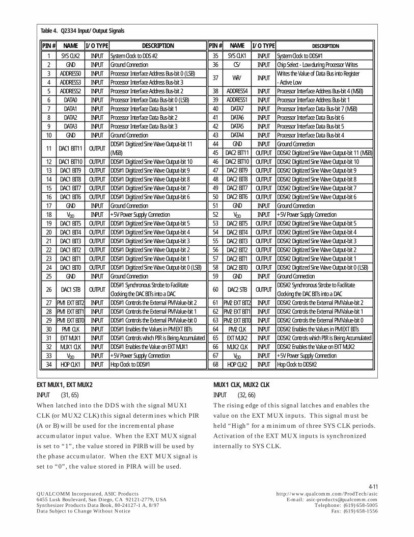
4-11QUALCOMM Incorporated, ASIC Products http://www.qualcomm.com/ProdTech/asic6455 Lusk Boulevard, San Diego, CA 92121-2779, USA E-mail: [email protected] Products Data Book, 80-24127-1 A, 8/97 Telephone: (619) 658-5005Data Subject to Change Without Notice Fax: (619) 658-1556
EXT MUX1, EXT MUX2INPUT (31, 65)
When latched into the DDS with the signal MUX1
CLK (or MUX2 CLK) this signal determines which PIR
(A or B) will be used for the incremental phase
accumulator input value. When the EXT MUX signal
is set to “1”, the value stored in PIRB will be used by
the phase accumulator. When the EXT MUX signal is
set to “0”, the value stored in PIRA will be used.
MUX1 CLK, MUX2 CLKINPUT (32, 66)
The rising edge of this signal latches and enables the
value on the EXT MUX inputs. This signal must be
held “High” for a minimum of three SYS CLK periods.
Activation of the EXT MUX inputs is synchronized
internally to SYS CLK.
Table 4. Q2334 Input/Output Signals
DESCRIPTIONPIN #
12345678910
11
1213141516171819202122232425
26
2728293031323334
NAME
SYS CLK2GND
ADDRESS0ADDRESS3ADDRESS2
DATA0DATA1DATA2DATA3GND
DAC1 BIT11
DAC1 BIT10DAC1 BIT9DAC1 BIT8DAC1 BIT7DAC1 BIT6
GNDVDD
DAC1 BIT5DAC1 BIT4DAC1 BIT3DAC1 BIT2DAC1 BIT1DAC1 BIT0
GND
DAC1 STB
PM1 EXT BIT2PM1 EXT BIT1PM1 EXT BIT0
PM1 CLKEXT MUX1MUX1 CLK
VDD
HOP CLK1
I/O TYPE
INPUTINPUTINPUTINPUTINPUTINPUTINPUTINPUTINPUTINPUT
OUTPUT
OUTPUTOUTPUTOUTPUTOUTPUTOUTPUTINPUTINPUT
OUTPUTOUTPUTOUTPUTOUTPUTOUTPUTOUTPUTINPUT
OUTPUT
INPUTINPUTINPUTINPUTINPUTINPUTINPUTINPUT
DESCRIPTION
System Clock to DDS #2Ground ConnectionProcessor Interface Address Bus-bit 0 (LSB)Processor Interface Address Bus-bit 3Processor Interface Address Bus-bit 2Processor Interface Data Bus-bit 0 (LSB)Processor Interface Data Bus-bit 1Processor Interface Data Bus-bit 2Processor Interface Data Bus-bit 3Ground ConnectionDDS#1 Digitized Sine Wave Output-bit 11(MSB)DDS#1 Digitized Sine Wave Output-bit 10DDS#1 Digitized Sine Wave Output-bit 9DDS#1 Digitized Sine Wave Output-bit 8DDS#1 Digitized Sine Wave Output-bit 7DDS#1 Digitized Sine Wave Output-bit 6Ground Connection+5V Power Supply ConnectionDDS#1 Digitized Sine Wave Output-bit 5DDS#1 Digitized Sine Wave Output-bit 4DDS#1 Digitized Sine Wave Output-bit 3DDS#1 Digitized Sine Wave Output-bit 2DDS#1 Digitized Sine Wave Output-bit 1DDS#1 Digitized Sine Wave Output-bit 0 (LSB)Ground ConnectionDDS#1 Synchronous Strobe to FacilitateClocking the DAC BITs into a DACDDS#1 Controls the External PM Value-bit 2DDS#1 Controls the External PM Value-bit 1DDS#1 Controls the External PM Value-bit 0DDS#1 Enables the Values in PM EXT BITsDDS#1 Controls which PIR is Being AccumulatedDDS#1 Enables the Value on EXT MUX1+5V Power Supply ConnectionHop Clock to DDS#1
PIN #
3536
37
38394041424344454647484950515253545556575859
60
6162636465666768
NAME
SYS CLK1CS/
WR/
ADDRESS4ADDRESS1
DATA7DATA6DATA5DATA4GND
DAC2 BIT11DAC2 BIT10DAC2 BIT9DAC2 BIT8DAC2 BIT7DAC2 BIT6
GNDVDD
DAC2 BIT5DAC2 BIT4DAC2 BIT3DAC2 BIT2DAC2 BIT1DAC2 BIT0
GND
DAC2 STB
PM2 EXT BIT2PM2 EXT BIT1PM2 EXT BIT0
PM2 CLKEXT MUX2MUX2 CLK
VDD
HOP CLK2
I/O TYPE
INPUTINPUT
INPUT
INPUTINPUTINPUTINPUTINPUTINPUTINPUT
OUTPUTOUTPUTOUTPUTOUTPUTOUTPUTOUTPUTINPUTINPUT
OUTPUTOUTPUTOUTPUTOUTPUTOUTPUTOUTPUTINPUT
OUTPUT
INPUTINPUTINPUTINPUTINPUTINPUTINPUTINPUT
System Clock to DDS#1Chip Select - Low during Processor WritesWrites the Value of Data Bus into Register- Active LowProcessor Interface Address Bus-bit 4 (MSB)Processor Interface Address Bus-bit 1Processor Interface Data Bus-bit 7 (MSB)Processor Interface Data Bus-bit 6Processor Interface Data Bus-bit 5Processor Interface Data Bus-bit 4Ground ConnectionDDS#2 Digitized Sine Wave Output-bit 11 (MSB)DDS#2 Digitized Sine Wave Output-bit 10DDS#2 Digitized Sine Wave Output-bit 9DDS#2 Digitized Sine Wave Output-bit 8DDS#2 Digitized Sine Wave Output-bit 7DDS#2 Digitized Sine Wave Output-bit 6Ground Connection+5V Power Supply ConnectionDDS#2 Digitized Sine Wave Output-bit 5DDS#2 Digitized Sine Wave Output-bit 4DDS#2 Digitized Sine Wave Output-bit 3DDS#2 Digitized Sine Wave Output-bit 2DDS#2 Digitized Sine Wave Output-bit 1DDS#2 Digitized Sine Wave Output-bit 0 (LSB)Ground ConnectionDDS#2 Synchronous Strobe to FacilitateClocking the DAC BITs into a DACDDS#2 Controls the External PM Value-bit 2DDS#2 Controls the External PM Value-bit 1DDS#2 Controls the External PM Value-bit 0DDS#2 Enables the Values in PM EXT BITsDDS#2 Controls which PIR is Being AccumulatedDDS#2 Enables the Value on EXT MUX2+5V Power Supply ConnectionHop Clock to DDS#2
4-12QUALCOMM Incorporated, ASIC Products http://www.qualcomm.com/ProdTech/asic6455 Lusk Boulevard, San Diego, CA 92121-2779, USA E-mail: [email protected] Products Data Book, 80-24127-1 A, 8/97 Telephone: (619) 658-5005Data Subject to Change Without Notice Fax: (619) 658-1556
PM1 EXT BIT0…PM1 EXT BIT2,PM2 EXT BIT0…PM2 EXT BIT2INPUTS (29, 28, 27, 63, 62, 61)
External phase modulation inputs which control 45
degree phase offsets in the phase accumulated values
in accordance with the settings provided in Table 3.
PM EXT BITs are active when the signal PM CLK is
asserted and are synchronized internally to the DDS
function to SYS CLK.
PM1 CLK, PM2 CLKINPUT (30, 64)
The rising edge of this signal latches and enables the
value on the PM EXT BIT inputs. This signal must be
held “High” for a minimum of three SYS CLK periods.
The PM EXT BIT inputs are synchronized internally to
SYS CLK.
DAC1 BIT0…DAC1 BIT11, DAC2 BIT0…DAC2 BIT11OUTPUTS (24, 23, 22, 21, 20, 19, 16, 15, 14, 13, 12, 11, 58, 57, 56, 55,
54, 53, 50, 49, 48, 47, 46, 45)
Digitized sine wave outputs encoded in offset binary or
two’s complement format, depending on settings in
the AMC Registers. One sample is generated during
each period of SYS CLK. DAC BIT 0 is the LSB.
DAC1 STB, DAC2 STBOUTPUT (26, 60)
Provides a synchronous strobe to facilitate clocking of
the DAC BIT outputs into an external register or
sampled DAC. One DAC STB is generated during
each period of SYS CLK. Essentially, the DAC STB (or
DAC STB/) is a delayed version of SYS CLK.
MODES OF OPERATIONEach DDS can be independently set to perform a wide
range of expanded functions of the basic operation, as
described in the following paragraphs.
BASIC SYNTHESIZER MODEIn its most Basic Operational Mode, each DDS on the
Q2334 can provide a fixed frequency digitized sine
wave output. The frequency of this sine output is
determined by the frequency of the clock input and the
value stored in the PIRs. (See formula (1) in the Phase
Increment Value section of the General DDS section.)
To set the Q2334 up in a Single Frequency Output
Mode, the SMC should be set to “00” (hex). The
AMC should be set according to the size of the DAC
selected and the desired output format. The PMAE
bit should also be set to “0”. (Refer to the Simple
Oscillator Mode Example section.)
PHASE MODULATION MODEThe Q2334 provides two means to implement phase
modulation of a basic frequency output, referred to as
Internal Phase Modulation and External Phase
Modulation.
Internal Phase Modulation provides extremely fine
resolution up to 0.00000008° of the phase adjustment
(232 - state phase resolution), while External Phase
Modulation is designed for 45° increment phase shifts.
INTERNAL PHASE MODULATIONInternal Phase Modulation operates as a differential
phase adjustment technique and requires use of the
processor interface. The Internal Phase Modulation
Mode is activated by loading PIRA with the correct
phase increment for the basic frequency without phase
modulation. PIRB is then loaded with the phase
increment value equal to the phase increment value
stored in PIRA plus the value of the desired phase
offset. The phase accumulator uses PIRA for most
phase accumulations.
Setting the HPME bit in the SMC register to logic
“1” arms the DDS to use the 32-bit value in PIRB for
one phase accumulation cycle when the signal HOP
CLK is asserted. Since the phase increment value in
PIRB is only used once for each HOP CLK assertion,
the net effect is to cause a phase change to the
generated sine wave.
When the PMAE bit is set to logic “1”, the 8 MSB
of PIRB are added to the 8 MSB of PIRA to form the
8 MSB to be accumulated with the 24 LSB of PIRA.
This 32-bit value is used for one-time accumulation. If
PMAE is “0”, all 32 units of PIRB will be used for the
accumulation.
4-13QUALCOMM Incorporated, ASIC Products http://www.qualcomm.com/ProdTech/asic6455 Lusk Boulevard, San Diego, CA 92121-2779, USA E-mail: [email protected] Products Data Book, 80-24127-1 A, 8/97 Telephone: (619) 658-5005Data Subject to Change Without Notice Fax: (619) 658-1556
The one-time phase shift occurs every time the
HOP CLK signal is asserted. The phase shift can
occur as often as the HOP CLK signal can be asserted.
(Refer to Processor Interface Timing shown in Figure 8
and Table 7).
If it is desired to change the phase offset value, PIRB
must be reloaded before the HOP CLK cycle with the
new phase offset for the next HOP CLK period. The
HPME bit will remain set to “1” until reset by the
processor. (Refer to the Hop Clock Phase Modulation
Enable section.)
EXTERNAL PHASE MODULATIONExternal Phase Modulation operates as an absolute
phase adjustment technique and utilizes special
synchronous inputs separate from the processor
interface. When using the External Phase Modulation
Mode, the phase increment value for the unmodulated
input is written into PIRA. PIRB is not used in the
External Phase Modulation Mode.
The External Phase Modulation Enable (EPME) bit
in the SMC register is set to logic “1” to enable the
External Phase Modulation Mode. When the EPME bit
is set to “1”, the phase offset determined by the PM
EXT BITs are latched into the DDS function each time
the signal PM CLK is asserted. This PM EXT BIT
setting causes a phase offset in 45° increments as
indicated in Table 3. This mode of operation allows
very simple control of the DDS as a binary, quartenary,
or 8-ary phase shift keyed (8PSK) modulator.
BINARY FREQUENCY SHIFT KEYING (BFSK) MODULATIONMODETwo PIRs are provided for each DDS function allowing
for Binary Frequency Shift Keyed (BFSK) modulation
without any additional hardware. The Q2334 provides
signals allowing this switch to occur synchronously.
BFSK Modulation is achieved by setting the phase
increment value in PIRA to generate the first
frequency and the value in the PIRB to generate the
second frequency. The EME bit is then set to logic “1”
to enable the external multiplexer controls.
If the EXT MUX signal is set to logic “1” when the
MUX CLK signal is asserted, the phase accumulator
will choose the phase increment value from PIRB. If
the EXT MUX signal is set to logic “0” when the MUX
CLK is asserted, the phase accumulator will choose the
phase increment value from PIRA. Changing the
value of the EXT MUX input causes the alternation
between the frequency controlled by PIRA and the
frequency controlled by PIRB.
After the BFSK Mode is set up and the PIRA and
PIRB contents are active, the EXT MUX signal can be
changed as fast as the MUX CLK can be asserted. (See
External Control Timing shown in Figure 10 and
Table 9). The MUX CLK timing is the only restriction
on how fast the accumulation can be switched from
PIRA to PIRB.
MINIMUM SHIFT KEYING (MSK) MODULATION MODEThe Minimum Shift Keying (MSK) Modulation Mode
is a subset of the BFSK Mode described above. The
operation is the same, but the two frequencies are
selected at a known mathematically determined rate.
The MSK Modulation Mode is linear MSK and can be
generated by setting the frequency shift rate equal to
the separation between the two frequencies. This is
where MSK got its name, since it is the minimum
spacing between the two frequencies that can be
accomplished while still recovering the signal with a
given shift rate. If the frequency spacing is closer than
the frequency shift rate, the information cannot be
recovered. If the spacing is too far apart, the
information can be retrieved using FSK demodulation
techniques, although MSK will not be generated from
the resultant spectra. To produce the two MSK
frequencies, the values in PIRA and PIRB correspond to
incrementing and decrementing phase values
(respectively) that must change through ±90 degrees for
each symbol time of the frequency shift rate. This is
obtained by loading PIRA and PIRB with frequency
values such that the mid-point value between them is
separated by ± FSK rate/2. This must occur without
any phase discontinuities but since the DDS changes
frequencies in a phase continuous fashion, this is not a
problem. The overall result due to the slow phase
transitions between the frequencies is a reduction in
the high-frequency spectral content, thus attenuating
4-14QUALCOMM Incorporated, ASIC Products http://www.qualcomm.com/ProdTech/asic6455 Lusk Boulevard, San Diego, CA 92121-2779, USA E-mail: [email protected] Products Data Book, 80-24127-1 A, 8/97 Telephone: (619) 658-5005Data Subject to Change Without Notice Fax: (619) 658-1556
the sidelobes. The spectrum is said to be more
efficient since more power is contained in the main
lobe and less in the sidelobes. The EME bit of the
SMC register is set to logic “1”, as in the BFSK Mode,
and the EXT MUX and MUX CLK signals control the
shift between the values of PIRA and PIRB.
FREQUENCY HOPPING MODESimple frequency hopping can be enabled by writing a
new phase increment value of the desired frequency in
PIRA. Since PIRA is a double buffered register, this
value will be activated at the next assertion of the
HOP CLK signal.
Assuming each frequency to be generated requires
all 32 bits to be changed, then four 8-bit writes to PIRA
would be needed. (See Processor Interface Timing
shown in Figure 8 and Table 7.) After PIRA has been
loaded, the assertion of the HOP CLK will activate
these settings and the resulting frequency will be
output from the Q2334 within 31 clock cycles. The
frequency value can be changed as fast as the new
phase increment value can be written to PIRA and a
HOP CLK signal asserted. (Also see Figure 8 and
Table 7.) Once all 32 bits have been activated, the
contents will remain until the register is written again.
Subsets within the register may also be written. This
allows for the changing of an existing register value
using a single 8-bit write as opposed to four 8-bit
writes.
PIPELINE DELAYThe output of the Q2334 DDS will reflect the change
in status activated by the HOP CLK within 30 to 31
SYS CLK periods. When the EXT MUX signal is
enabled, the associated PIR will affect the output in
29 to 30 SYS CLK periods after the MUX CLK has
been asserted. If External Phase Modulation is
implemented, the phase shift will occur 28 to 29
SYS CLK periods after the rising of the PM CLK.
The one SYS CLK ambiguity occurs because the
MUX CLK, PM CLK, and HOP CLK signals are
allowed to be asynchronous in relation to the SYS
CLK. To keep the internal operation of the Q2334
synchronous, the signals are input to synchronizing
circuitry which resolves the signal to within one clock
period.
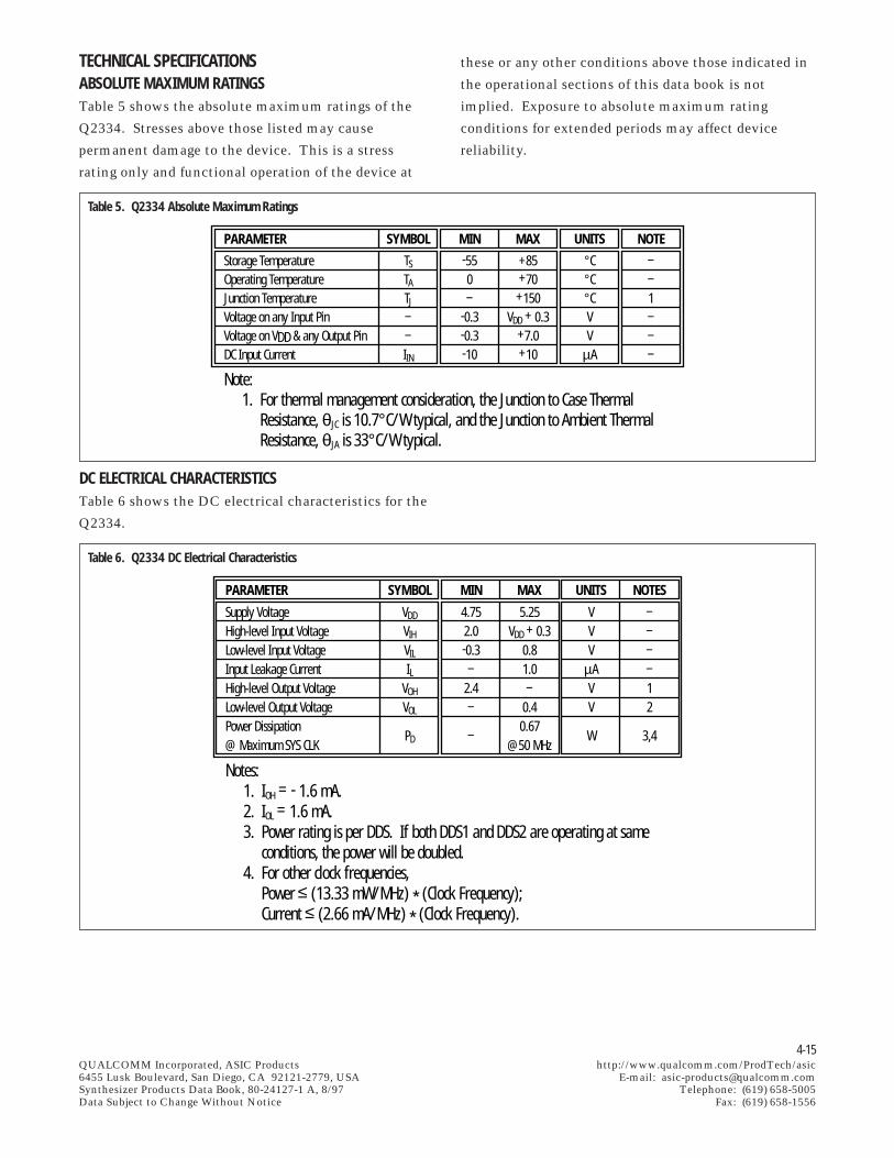
4-15QUALCOMM Incorporated, ASIC Products http://www.qualcomm.com/ProdTech/asic6455 Lusk Boulevard, San Diego, CA 92121-2779, USA E-mail: [email protected] Products Data Book, 80-24127-1 A, 8/97 Telephone: (619) 658-5005Data Subject to Change Without Notice Fax: (619) 658-1556
TECHNICAL SPECIFICATIONSABSOLUTE MAXIMUM RATINGSTable 5 shows the absolute maximum ratings of the
Q2334. Stresses above those listed may cause
permanent damage to the device. This is a stress
rating only and functional operation of the device at
these or any other conditions above those indicated in
the operational sections of this data book is not
implied. Exposure to absolute maximum rating
conditions for extended periods may affect device
reliability.
Table 5. Q2334 Absolute Maximum Ratings
PARAMETER
Storage TemperatureOperating TemperatureJunction TemperatureVoltage on any Input PinVoltage on VDD & any Output PinDC Input Current
Note: 1. For thermal management consideration, the Junction to Case Thermal Resistance, θJC is 10.7°C/W typical, and the Junction to Ambient Thermal Resistance, θJA is 33°C/W typical.
SYMBOL
TS
TA
TJ
––IIN
MAX
+85+70
+150VDD + 0.3
+7.0+10
MIN-550–
-0.3-0.3-10
UNITS
°C°C°CVV
µA
NOTE––1–––
DC ELECTRICAL CHARACTERISTICSTable 6 shows the DC electrical characteristics for the
Q2334.
Table 6. Q2334 DC Electrical Characteristics
PARAMETER
Supply VoltageHigh-level Input VoltageLow-level Input VoltageInput Leakage CurrentHigh-level Output VoltageLow-level Output VoltagePower Dissipation@ Maximum SYS CLK
Notes: 1. IOH = - 1.6 mA. 2. IOL = 1.6 mA. 3. Power rating is per DDS. If both DDS1 and DDS2 are operating at same conditions, the power will be doubled. 4. For other clock frequencies, Power ≤ (13.33 mW/MHz) * (Clock Frequency); Current ≤ (2.66 mA/MHz) * (Clock Frequency).
SYMBOL
VDD
VIH
VIL
ILVOH
VOL
PD
MAX
5.25VDD + 0.3
0.81.0–
0.40.67
@50 MHz
MIN
4.752.0-0.3–
2.4–
–
NOTES––––12
3,4
UNITS
VVV
µAVV
W
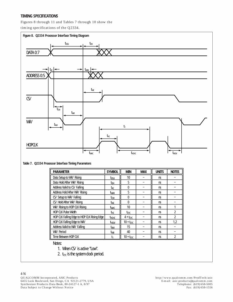
4-16QUALCOMM Incorporated, ASIC Products http://www.qualcomm.com/ProdTech/asic6455 Lusk Boulevard, San Diego, CA 92121-2779, USA E-mail: [email protected] Products Data Book, 80-24127-1 A, 8/97 Telephone: (619) 658-5005Data Subject to Change Without Notice Fax: (619) 658-1556
TIMING SPECIFICATIONSFigures 8 through 11 and Tables 7 through 10 show the
timing specifications of the Q2334.
Figure 8. Q2334 Processor Interface Timing Diagram
DATA 0:7
ADDRESS 0:5
CS/
WR/
HOPCLK
tDSU tDH
tAC tWAX
tWC
tCWtWR
tAW t1
tHC
tWHC tHCHC tHCW
Table 7. Q2334 Processor Interface Timing Parameters
PARAMETER
Data Setup to WR/ RisingData Hold After WR/ RisingAddress Valid to CS/ FallingAddress Hold After WR/ RisingCS/ Setup to WR/ FallingCS/ Hold After WR/ RisingWR/ Rising to HOP CLK RisingHOP CLK Pulse WidthHOP CLK Falling Edge to HOP CLK Rising EdgeHOP CLK Falling Edge to WR/Address Valid to WR/ FallingWR/ PeriodTime Between HOP CLK
Notes: 1. When CS/ is active "Low". 2. tCYC is the system clock period.
SYMBOL
tDSU
tDH
tAC
tWAX
tCW
tWC
tWHC
tHC
tHCHC
tHCW
tAW
tWR
t1
MIN
105050010tCYC
4 * tCYC
10 * tCYC
1540
10 * tCYC
MAX–––––––––––––
NOTES––––––122
1,2––2
UNITS
nsnsnsnsnsnsnsnsnsnsnsnsns
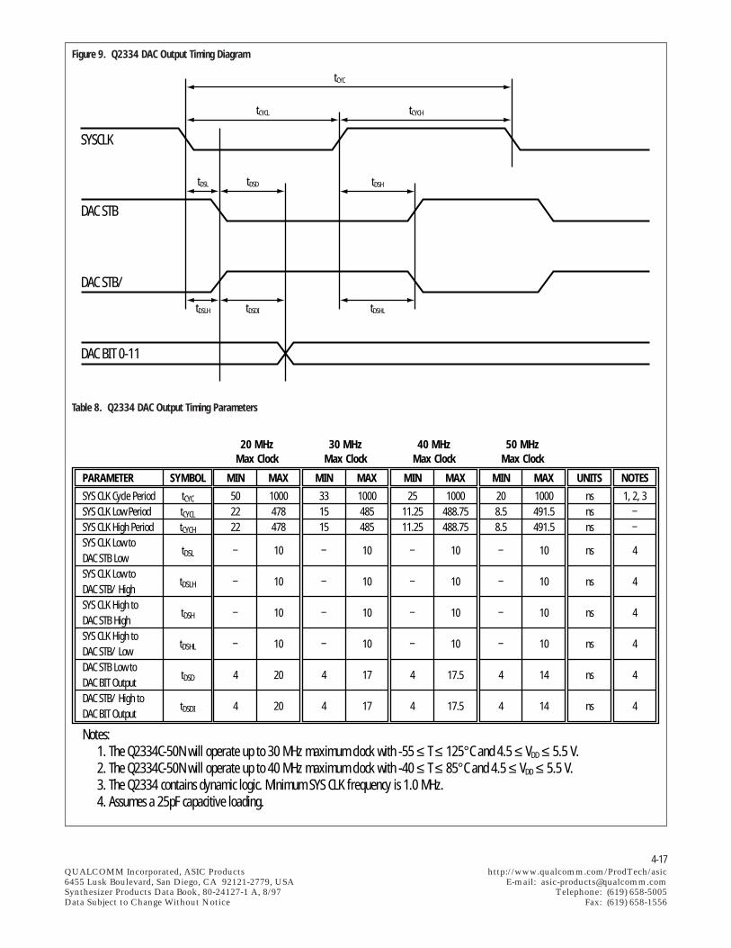
4-17QUALCOMM Incorporated, ASIC Products http://www.qualcomm.com/ProdTech/asic6455 Lusk Boulevard, San Diego, CA 92121-2779, USA E-mail: [email protected] Products Data Book, 80-24127-1 A, 8/97 Telephone: (619) 658-5005Data Subject to Change Without Notice Fax: (619) 658-1556
Figure 9. Q2334 DAC Output Timing Diagram
tCYC
SYSCLK
DAC STB
DAC STB/
DAC BIT 0-11
tCYCL tCYCH
tDSHtDSL tDSD
tDSLH tDSDI tDSHL
Table 8. Q2334 DAC Output Timing Parameters
PARAMETER
SYS CLK Cycle PeriodSYS CLK Low PeriodSYS CLK High PeriodSYS CLK Low to DAC STB LowSYS CLK Low to DAC STB/ HighSYS CLK High to DAC STB HighSYS CLK High to DAC STB/ LowDAC STB Low to DAC BIT OutputDAC STB/ High to DAC BIT Output
Notes: 1. The Q2334C-50N will operate up to 30 MHz maximum clock with -55 ≤ T ≤ 125°C and 4.5 ≤ VDD ≤ 5.5 V. 2. The Q2334C-50N will operate up to 40 MHz maximum clock with -40 ≤ T ≤ 85°C and 4.5 ≤ VDD ≤ 5.5 V. 3. The Q2334 contains dynamic logic. Minimum SYS CLK frequency is 1.0 MHz. 4. Assumes a 25pF capacitive loading.
SYMBOL
tCYC
tCYCL
tCYCH
tDSL
tDSLH
tDSH
tDSHL
tDSD
tDSDI
MIN
502222
–
–
–
–
4
4
MAX
1000478478
10
10
10
10
20
20
MAX
1000485485
10
10
10
10
17
17
MIN
331515
–
–
–
–
4
4
NOTES
1, 2, 3––
4
4
4
4
4
4
UNITS
nsnsns
ns
ns
ns
ns
ns
ns
20 MHzMax Clock
30 MHzMax Clock
MAX
1000488.75488.75
10
10
10
10
17.5
17.5
MIN
2511.2511.25
–
–
–
–
4
4
40 MHzMax Clock
MAX
1000491.5491.5
10
10
10
10
14
14
MIN
208.58.5
–
–
–
–
4
4
50 MHzMax Clock
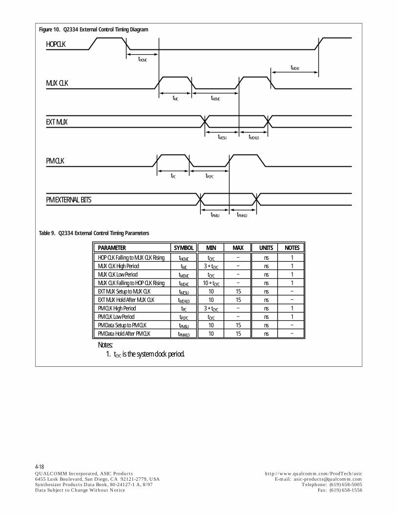
4-18QUALCOMM Incorporated, ASIC Products http://www.qualcomm.com/ProdTech/asic6455 Lusk Boulevard, San Diego, CA 92121-2779, USA E-mail: [email protected] Products Data Book, 80-24127-1 A, 8/97 Telephone: (619) 658-5005Data Subject to Change Without Notice Fax: (619) 658-1556
Figure 10. Q2334 External Control Timing Diagram
HOPCLK
MUX CLK
EXT MUX
PM CLK
PM EXTERNAL BITS
tHCMC
tMC tMCMC
tMCHC
tMCSU tMCHLD
tPC tPCPC
tPMSU tPMHLD
Table 9. Q2334 External Control Timing Parameters
PARAMETER
HOP CLK Falling to MUX CLK RisingMUX CLK High PeriodMUX CLK Low PeriodMUX CLK Falling to HOP CLK RisingEXT MUX Setup to MUX CLKEXT MUX Hold After MUX CLKPM CLK High PeriodPM CLK Low PeriodPM Data Setup to PM CLKPM Data Hold After PM CLK
Notes: 1. tCYC is the system clock period.
SYMBOL
tHCMC
tMC
tMCMC
tMCHC
tMCSU
tMCHLD
tPC
tPCPC
tPMSU
tPMHLD
MIN
tCYC
3 * tCYC
tCYC
10 * tCYC
1010
3 * tCYC
tCYC
1010
MAX––––1515––1515
UNITS
nsnsnsnsnsnsnsnsnsns
NOTES
1111––11––
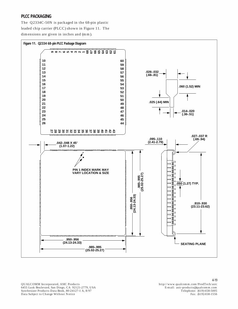
4-19QUALCOMM Incorporated, ASIC Products http://www.qualcomm.com/ProdTech/asic6455 Lusk Boulevard, San Diego, CA 92121-2779, USA E-mail: [email protected] Products Data Book, 80-24127-1 A, 8/97 Telephone: (619) 658-5005Data Subject to Change Without Notice Fax: (619) 658-1556
PLCC PACKAGINGThe Q2334C-50N is packaged in the 68-pin plastic
leaded chip carrier (PLCC) shown in Figure 11. The
dimensions are given in inches and (mm).
Figure 11. Q2334 68-pin PLCC Package Diagram
.026-.032(.66-.81)
.060 (1.52) MIN
.025 (.64) MIN
.014-.020(.36-.51)
6059585756555453525150494847464544
1011121314151617181920212223242526
9 8 7 6 5 4 3 2 1 68 67 66 65 64 63 62 61
4342414039383736353433323130292827
.950-.956(24.13-24.33)
.985-.995(25.02-25.27)
.985
-.99
5(2
5.02
-25.
27)
.950
-.95
6(2
4.13
-24.
33)
.042-.048 X 45°(1.07-1.22)
.095-.110(2.41-2.79)
.027-.037 R(.69-.94)
.050 (1.27) TYP.
.910-.930(23.11-23.62)
SEATING PLANE
••
PIN 1 INDEX MARK MAYVARY LOCATION & SIZE
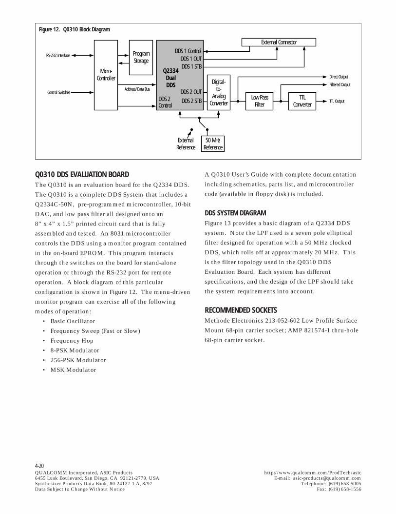
4-20QUALCOMM Incorporated, ASIC Products http://www.qualcomm.com/ProdTech/asic6455 Lusk Boulevard, San Diego, CA 92121-2779, USA E-mail: [email protected] Products Data Book, 80-24127-1 A, 8/97 Telephone: (619) 658-5005Data Subject to Change Without Notice Fax: (619) 658-1556
Q0310 DDS EVALUATION BOARDThe Q0310 is an evaluation board for the Q2334 DDS.
The Q0310 is a complete DDS System that includes a
Q2334C-50N, pre-programmed microcontroller, 10-bit
DAC, and low pass filter all designed onto an
8” x 4” x 1.5” printed circuit card that is fully
assembled and tested. An 8031 microcontroller
controls the DDS using a monitor program contained
in the on-board EPROM. This program interacts
through the switches on the board for stand-alone
operation or through the RS-232 port for remote
operation. A block diagram of this particular
configuration is shown in Figure 12. The menu-driven
monitor program can exercise all of the following
modes of operation:
• Basic Oscillator
• Frequency Sweep (Fast or Slow)
• Frequency Hop
• 8-PSK Modulator
• 256-PSK Modulator
• MSK Modulator
Figure 12. Q0310 Block Diagram
Q2334DualDDS
TTLConverter
RS-232 Interface
Control Switches
Micro-Controller
ProgramStorage
DDS 1 ControlDDS 1 OUTDDS 1 STB
DDS 2 OUTDDS 2 STBDDS 2
Control
Address/Data Bus
Digital-to-
AnalogConverter
Low PassFilter
TTL Output
Filtered Output
Direct Output
External Connector
50 MHzReference
ExternalReference
A Q0310 User’s Guide with complete documentation
including schematics, parts list, and microcontroller
code (available in floppy disk) is included.
DDS SYSTEM DIAGRAMFigure 13 provides a basic diagram of a Q2334 DDS
system. Note the LPF used is a seven pole elliptical
filter designed for operation with a 50 MHz clocked
DDS, which rolls off at approximately 20 MHz. This
is the filter topology used in the Q0310 DDS
Evaluation Board. Each system has different
specifications, and the design of the LPF should take
the system requirements into account.
RECOMMENDED SOCKETSMethode Electronics 213-052-602 Low Profile Surface
Mount 68-pin carrier socket; AMP 821574-1 thru-hole
68-pin carrier socket.
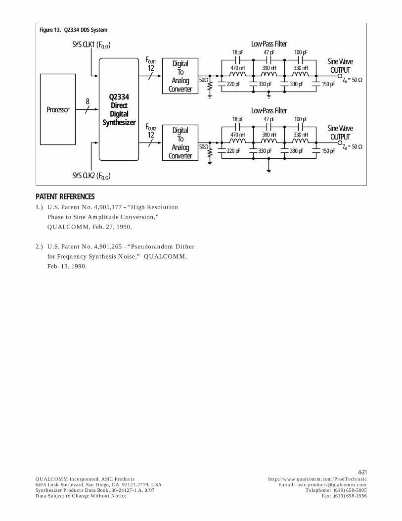
4-21QUALCOMM Incorporated, ASIC Products http://www.qualcomm.com/ProdTech/asic6455 Lusk Boulevard, San Diego, CA 92121-2779, USA E-mail: [email protected] Products Data Book, 80-24127-1 A, 8/97 Telephone: (619) 658-5005Data Subject to Change Without Notice Fax: (619) 658-1556
Figure 13. Q2334 DDS System
Q2334DirectDigital
Synthesizer
Processor8
SYS CLK1 (FCLK1)
SYS CLK2 (FCLK2)
FOUT1
12
FOUT2
12
DigitalTo
AnalogConverter
50Ω220 pF 330 pF 330 pF 150 pF
390 nH470 nH 330 nH
18 pF 47 pF 100 pF
220 pF 330 pF 330 pF 150 pF
390 nH470 nH 330 nH
18 pF 47 pF 100 pF
Low-Pass Filter
Sine WaveOUTPUT
Z0 = 50 Ω
DigitalTo
AnalogConverter
50Ω
Low-Pass Filter
Sine WaveOUTPUT
Z0 = 50 Ω
PATENT REFERENCES1.) U.S. Patent No. 4,905,177 - “High Resolution
Phase to Sine Amplitude Conversion,”
QUALCOMM, Feb. 27, 1990.
2.) U.S. Patent No. 4,901,265 - “Pseudorandom Dither
for Frequency Synthesis Noise,” QUALCOMM,
Feb. 13, 1990.
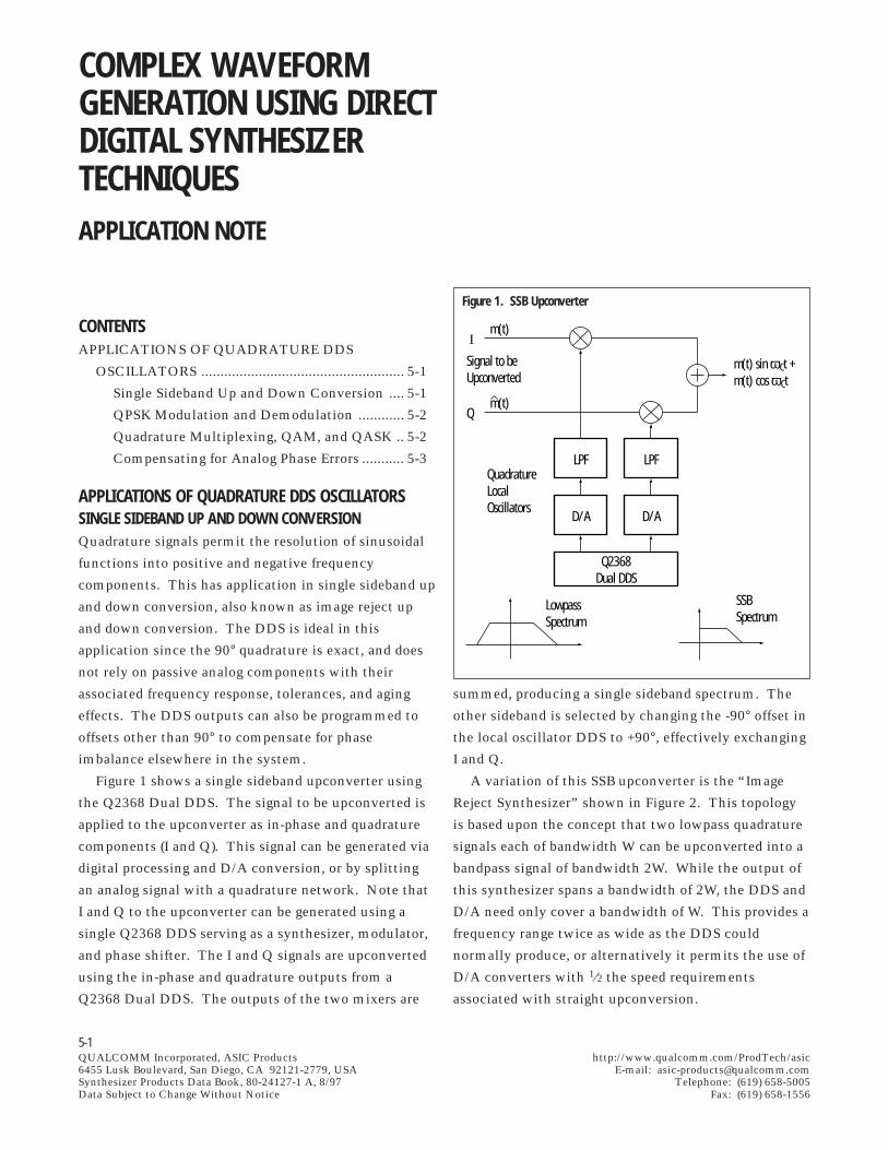
5-1QUALCOMM Incorporated, ASIC Products http://www.qualcomm.com/ProdTech/asic6455 Lusk Boulevard, San Diego, CA 92121-2779, USA E-mail: [email protected] Products Data Book, 80-24127-1 A, 8/97 Telephone: (619) 658-5005Data Subject to Change Without Notice Fax: (619) 658-1556
COMPLEX WAVEFORMGENERATION USING DIRECTDIGITAL SYNTHESIZERTECHNIQUESAPPLICATION NOTE
summed, producing a single sideband spectrum. The
other sideband is selected by changing the -90° offset in
the local oscillator DDS to +90°, effectively exchanging
I and Q.
A variation of this SSB upconverter is the “Image
Reject Synthesizer” shown in Figure 2. This topology
is based upon the concept that two lowpass quadrature
signals each of bandwidth W can be upconverted into a
bandpass signal of bandwidth 2W. While the output of
this synthesizer spans a bandwidth of 2W, the DDS and
D/A need only cover a bandwidth of W. This provides a
frequency range twice as wide as the DDS could
normally produce, or alternatively it permits the use of
D/A converters with 1⁄2 the speed requirements
associated with straight upconversion.
APPLICATIONS OF QUADRATURE DDS OSCILLATORSSINGLE SIDEBAND UP AND DOWN CONVERSIONQuadrature signals permit the resolution of sinusoidal
functions into positive and negative frequency
components. This has application in single sideband up
and down conversion, also known as image reject up
and down conversion. The DDS is ideal in this
application since the 90° quadrature is exact, and does
not rely on passive analog components with their
associated frequency response, tolerances, and aging
effects. The DDS outputs can also be programmed to
offsets other than 90° to compensate for phase
imbalance elsewhere in the system.
Figure 1 shows a single sideband upconverter using
the Q2368 Dual DDS. The signal to be upconverted is
applied to the upconverter as in-phase and quadrature
components (I and Q). This signal can be generated via
digital processing and D/A conversion, or by splitting
an analog signal with a quadrature network. Note that
I and Q to the upconverter can be generated using a
single Q2368 DDS serving as a synthesizer, modulator,
and phase shifter. The I and Q signals are upconverted
using the in-phase and quadrature outputs from a
Q2368 Dual DDS. The outputs of the two mixers are
m(t) sin ωCt +m(t) cos ωCt
Q2368Dual DDS
D/A D/A
LPFQuadratureLocalOscillators
LowpassSpectrum
Signal to beUpconverted
Im(t)
m(t)Q
LPF
SSBSpectrum
Figure 1. SSB Upconverter
CONTENTSAPPLICATIONS OF QUADRATURE DDS
OSCILLATORS ..................................................... 5-1
Single Sideband Up and Down Conversion .... 5-1
QPSK Modulation and Demodulation ............ 5-2
Quadrature Multiplexing, QAM, and QASK .. 5-2
Compensating for Analog Phase Errors ........... 5-3
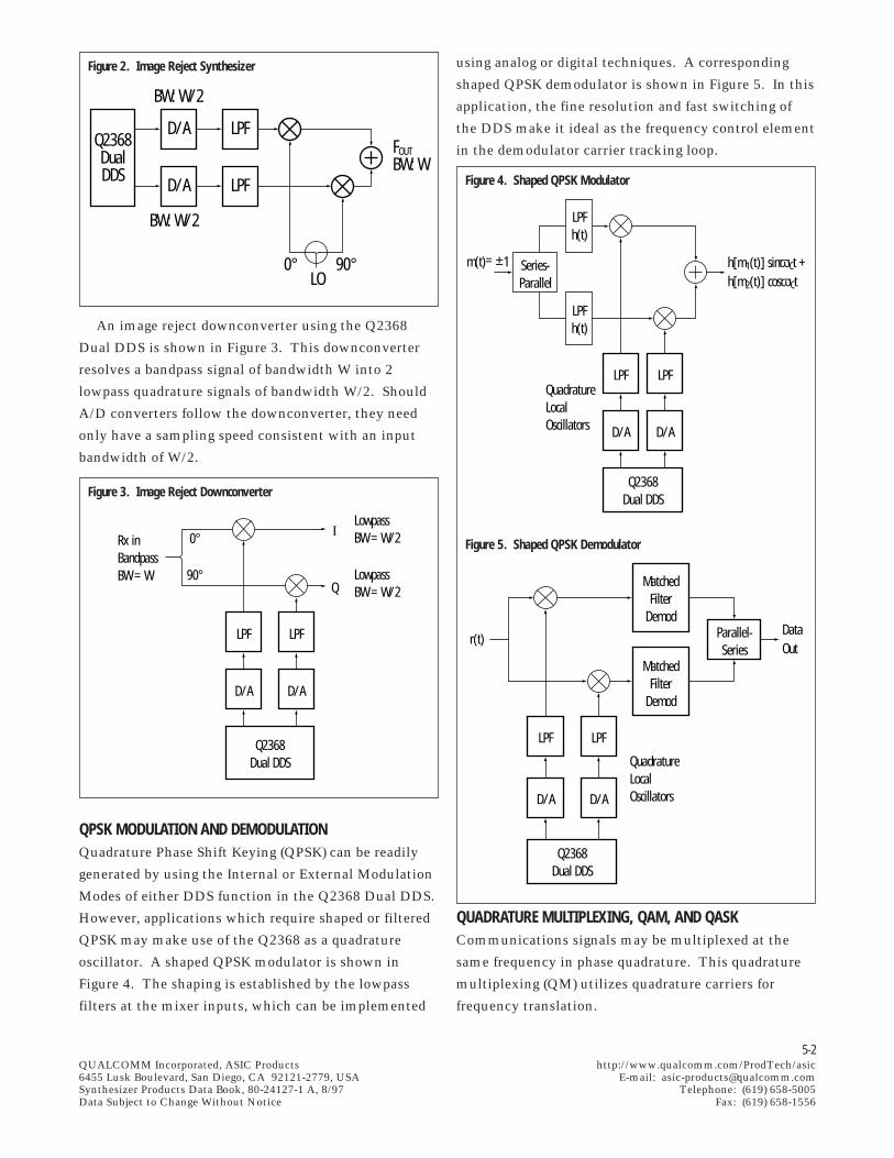
5-2QUALCOMM Incorporated, ASIC Products http://www.qualcomm.com/ProdTech/asic6455 Lusk Boulevard, San Diego, CA 92121-2779, USA E-mail: [email protected] Products Data Book, 80-24127-1 A, 8/97 Telephone: (619) 658-5005Data Subject to Change Without Notice Fax: (619) 658-1556
An image reject downconverter using the Q2368
Dual DDS is shown in Figure 3. This downconverter
resolves a bandpass signal of bandwidth W into 2
lowpass quadrature signals of bandwidth W/2. Should
A/D converters follow the downconverter, they need
only have a sampling speed consistent with an input
bandwidth of W/2.
Figure 2. Image Reject Synthesizer
Q2368DualDDS
D/A
BW: W/2
BW: W/2
D/A
LPF
LPF
LO90°0°
FOUT
BW: W
using analog or digital techniques. A corresponding
shaped QPSK demodulator is shown in Figure 5. In this
application, the fine resolution and fast switching of
the DDS make it ideal as the frequency control element
in the demodulator carrier tracking loop.
Figure 3. Image Reject Downconverter
Rx inBandpassBW = W
0°
90°
I
Q
LowpassBW = W/2
LowpassBW = W/2
Q2368Dual DDS
D/A D/A
LPF LPF
Figure 4. Shaped QPSK Modulator
h[m1(t)] sinωCt +h[m2(t)] cosωCt
m(t)= ±1
Q2368Dual DDS
D/A D/A
LPFQuadratureLocalOscillators
LPF
Series-Parallel
LPFh(t)
LPFh(t)
DataOut
r(t)
Q2368Dual DDS
D/A D/A
LPF
QuadratureLocalOscillators
LPF
MatchedFilter
Demod
MatchedFilter
Demod
Parallel-Series
QPSK MODULATION AND DEMODULATIONQuadrature Phase Shift Keying (QPSK) can be readily
generated by using the Internal or External Modulation
Modes of either DDS function in the Q2368 Dual DDS.
However, applications which require shaped or filtered
QPSK may make use of the Q2368 as a quadrature
oscillator. A shaped QPSK modulator is shown in
Figure 4. The shaping is established by the lowpass
filters at the mixer inputs, which can be implemented
Figure 5. Shaped QPSK Demodulator
QUADRATURE MULTIPLEXING, QAM, AND QASKCommunications signals may be multiplexed at the
same frequency in phase quadrature. This quadrature
multiplexing (QM) utilizes quadrature carriers for
frequency translation.
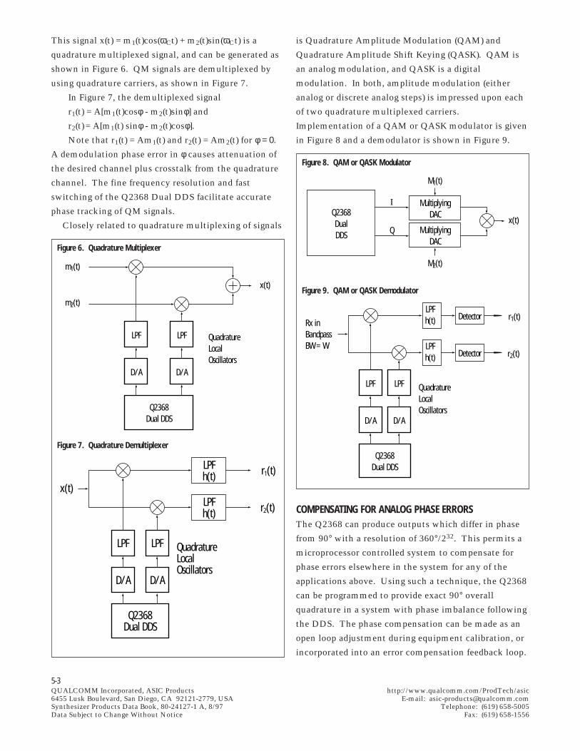
5-3QUALCOMM Incorporated, ASIC Products http://www.qualcomm.com/ProdTech/asic6455 Lusk Boulevard, San Diego, CA 92121-2779, USA E-mail: [email protected] Products Data Book, 80-24127-1 A, 8/97 Telephone: (619) 658-5005Data Subject to Change Without Notice Fax: (619) 658-1556
This signal x(t) = m1(t)cos(ωCt) + m2(t)sin(ωCt) is a
quadrature multiplexed signal, and can be generated as
shown in Figure 6. QM signals are demultiplexed by
using quadrature carriers, as shown in Figure 7.
In Figure 7, the demultiplexed signal
r1(t) = A[m1(t)cosφ - m2(t)sinφ] and
r2(t) = A[m1(t) sinφ - m2(t)cosφ].
Note that r1(t) = Am1(t) and r2(t) = Am2(t) for φ = 0.A demodulation phase error in φ causes attenuation of
the desired channel plus crosstalk from the quadrature
channel. The fine frequency resolution and fast
switching of the Q2368 Dual DDS facilitate accurate
phase tracking of QM signals.
Closely related to quadrature multiplexing of signals
is Quadrature Amplitude Modulation (QAM) and
Quadrature Amplitude Shift Keying (QASK). QAM is
an analog modulation, and QASK is a digital
modulation. In both, amplitude modulation (either
analog or discrete analog steps) is impressed upon each
of two quadrature multiplexed carriers.
Implementation of a QAM or QASK modulator is given
in Figure 8 and a demodulator is shown in Figure 9.
Figure 6. Quadrature Multiplexer
x(t)
m1(t)
m2(t)
Q2368Dual DDS
D/A D/A
LPF QuadratureLocalOscillators
LPF
x(t)
r1(t)
r2(t)
QuadratureLocalOscillators
Q2368Dual DDS
D/A D/A
LPF LPF
LPFh(t)
LPFh(t)
Figure 7. Quadrature Demultiplexer
Figure 8. QAM or QASK Modulator
Figure 9. QAM or QASK Demodulator
Q2368DualDDS
I
Q
MultiplyingDAC
M1(t)
M2(t)
MultiplyingDAC
x(t)
Rx inBandpassBW = W
r1(t)
r2(t)
QuadratureLocalOscillators
Q2368Dual DDS
D/A D/A
LPF LPF
LPFh(t)
LPFh(t)
Detector
Detector
COMPENSATING FOR ANALOG PHASE ERRORSThe Q2368 can produce outputs which differ in phase
from 90° with a resolution of 360°/232. This permits a
microprocessor controlled system to compensate for
phase errors elsewhere in the system for any of the
applications above. Using such a technique, the Q2368
can be programmed to provide exact 90° overall
quadrature in a system with phase imbalance following
the DDS. The phase compensation can be made as an
open loop adjustment during equipment calibration, or
incorporated into an error compensation feedback loop.
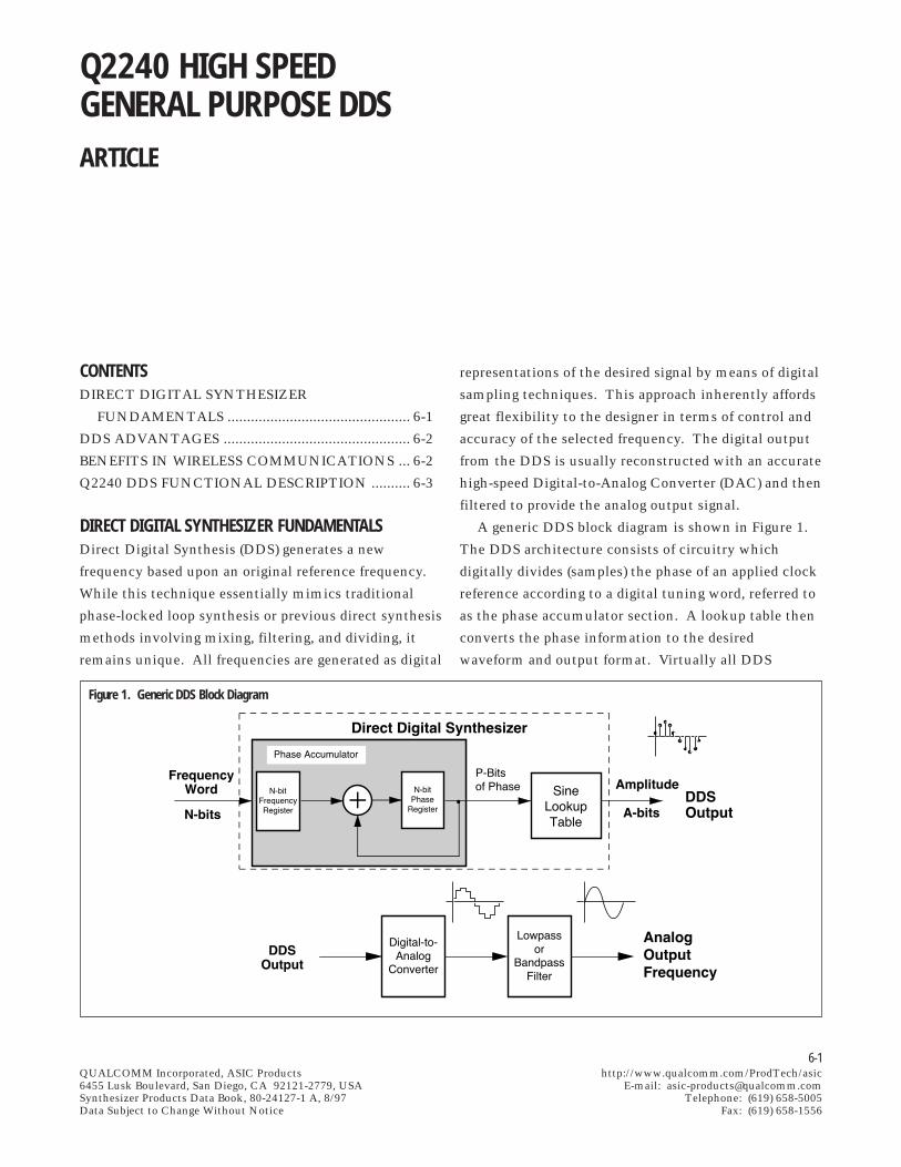
6-1QUALCOMM Incorporated, ASIC Products http://www.qualcomm.com/ProdTech/asic6455 Lusk Boulevard, San Diego, CA 92121-2779, USA E-mail: [email protected] Products Data Book, 80-24127-1 A, 8/97 Telephone: (619) 658-5005Data Subject to Change Without Notice Fax: (619) 658-1556
Q2240 HIGH SPEEDGENERAL PURPOSE DDSARTICLE
representations of the desired signal by means of digital
sampling techniques. This approach inherently affords
great flexibility to the designer in terms of control and
accuracy of the selected frequency. The digital output
from the DDS is usually reconstructed with an accurate
high-speed Digital-to-Analog Converter (DAC) and then
filtered to provide the analog output signal.
A generic DDS block diagram is shown in Figure 1.
The DDS architecture consists of circuitry which
digitally divides (samples) the phase of an applied clock
reference according to a digital tuning word, referred to
as the phase accumulator section. A lookup table then
converts the phase information to the desired
waveform and output format. Virtually all DDS
Figure 1. Generic DDS Block Diagram
DIRECT DIGITAL SYNTHESIZER FUNDAMENTALSDirect Digital Synthesis (DDS) generates a new
frequency based upon an original reference frequency.
While this technique essentially mimics traditional
phase-locked loop synthesis or previous direct synthesis
methods involving mixing, filtering, and dividing, it
remains unique. All frequencies are generated as digital
CONTENTSDIRECT DIGITAL SYNTHESIZER
FUNDAMENTALS ............................................... 6-1
DDS ADVANTAGES ................................................ 6-2
BENEFITS IN WIRELESS COMMUNICATIONS ... 6-2
Q2240 DDS FUNCTIONAL DESCRIPTION .......... 6-3
6-2QUALCOMM Incorporated, ASIC Products http://www.qualcomm.com/ProdTech/asic6455 Lusk Boulevard, San Diego, CA 92121-2779, USA E-mail: [email protected] Products Data Book, 80-24127-1 A, 8/97 Telephone: (619) 658-5005Data Subject to Change Without Notice Fax: (619) 658-1556
architectures include a lookup table which performs a
sine computation function for generating sinusoidal
output signals. Since the DDS chip contains all the
digital processing to construct and manipulate a
frequency, most analog circuitry is eliminated, along
with bothersome analog tolerances and aging effects.
The reconstructed analog output from the DAC retains
the same frequency stability and accuracy as the
applied clock reference. While this technique offers
many design benefits, there are a few drawbacks that
should be considered early in the design cycle. The
limitations imposed by the digital sampling process and
the digital-to-analog reconstruction affect three primary
areas of performance:
1. The maximum fundamental frequency that can be
generated is less than one-half of the applied clock
reference. Typical CMOS-based DDSs are
practicable at clock frequencies within the HF to
VHF frequency range.
2. Discrete spurious signals at the analog output may
be at a higher level than with other frequency
synthesis techniques. The choice of DAC to be
used with the DDS will overridingly determine the
output spectral purity.
3. DDS power consumption is directly proportional to
the frequency of the applied clock reference. Thus,
when operating at a higher clock rate for battery
operated or other power-constrained applications, a
DDS may not be suitable.
Although these potential performance liabilities
impose some practical limitations, the overall utility of
DDS will prominently stand out when selecting a
synthesizer method.
DDS ADVANTAGESSeveral capabilities set the DDS apart from other
frequency synthesis techniques and benefit the design
of digital wireless communication systems. In terms of
frequency step size or resolution, no other synthesis
method can achieve the frequency resolution control
that DDS provides. The frequency resolution is a
function of the applied clock reference and the number
of bits input to the phase accumulator, according to the
relation FS /2N , where FS is the system clock and N is
the number of bits in the phase accumulator. For
example, using a common 32-bit phase accumulator
equates to step sizes on the order of milli-hertz even at
clock frequencies in the VHF frequency range or above.
Another distinguishing characteristic of DDS is its
switching speed capability. Whereby PLL techniques
employ feedback and filtering of error signals impeding
the time required to change frequencies, a DDS is only
constrained by the digital interface control and the
settling time requirements of the DAC. DDSs switch
frequencies at rates on the order of nanoseconds or a
few microseconds, an improvement of at least one or
two orders of magnitude faster than conventional PLL
switching speeds. Moreover, all frequency changes are
automatically completed in a phase continuous fashion;
that is, a change to a new frequency continues in-phase
from the last point in the previous frequency. Since the
signal generated is in the digital domain, it can be
manipulated with exceptional versatility. For example,
when generating sinewaves, frequency and phase
modulation control (FSK or PSK) is easily implemented.
Alternatively, the DDS can generate arbitrary
waveforms by directing the output of the phase
accumulator into an external RAM or RAMDAC
instead of mapping it through the sine lookup table.
With this implementation, general waveform mapping
can create a variety of sophisticated signals such as
nonlinear-phase signals, synthesized music, and even
noise waveforms.
BENEFITS IN WIRELESS COMMUNICATIONSSynthesizer performance is a primary concern to the
wireless equipment designer. As the heart of the
system’s tuning, the synthesizer ultimately determines
the product’s compliance with many market-driven
requirements. A DDS may be the only practical
solution to achieve certain market-driven
requirements. From a technical as well as economic
standpoint, the DDS fills much of the criteria for an
ideal synthesizer design solution – a simple, highly
integrated, small, low-power circuit. Specifically, much
of the DDS functionality is software-configurable and
recent products offer many new built-in utility features.
Within their operating band, wireless systems now
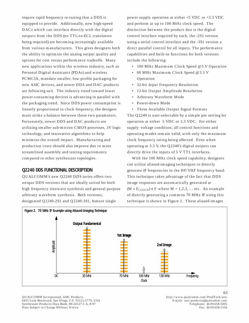
6-3QUALCOMM Incorporated, ASIC Products http://www.qualcomm.com/ProdTech/asic6455 Lusk Boulevard, San Diego, CA 92121-2779, USA E-mail: [email protected] Products Data Book, 80-24127-1 A, 8/97 Telephone: (619) 658-5005Data Subject to Change Without Notice Fax: (619) 658-1556
require rapid frequency re-tuning that a DDS is
equipped to provide. Additionally, new high-speed
DACs which can interface directly with the digital
outputs from the DDS (no TTL-to-ECL translators
being required) are becoming increasingly available
from various manufacturers. This gives designers both
the ability to optimize the analog output quality and
options for cost versus performance tradeoffs. Many
new applications within the wireless industry, such as
Personal Digital Assistants (PDAs) and wireless
PCMCIA, mandate smaller, low-profile packaging for
new ASIC devices, and newer DDS and DAC products
are following suit. The industry trend toward lower
power-consuming devices is advancing in parallel with
the packaging trend. Since DDS power consumption is
linearly proportional to clock frequency, the designer
must strike a balance between these two parameters.
Fortunately, newer DDS and DAC products are
utilizing smaller sub-micron CMOS processes, 3V logic
technology, and innovative algorithms to help
minimize the overall impact. Manufacturing and
production costs should also improve due to more
streamlined assembly and testing requirements
compared to other synthesizer topologies.
Q2240 DDS FUNCTIONAL DESCRIPTIONQUALCOMM’s new Q2240 DDS series offers two
unique DDS versions that are ideally suited for both
high frequency sinewave synthesis and general purpose
arbitrary waveform synthesis. Both versions,
designated Q2240-2S1 and Q2240-3S1, feature single
power supply operation at either +5 VDC or +3.3 VDC
and perform at up to 100 MHz clock speed. The
distinction between the product duo is the digital
control interface required by each, the -2S1 version
using a serial control interface and the -3S1 version a
direct parallel control for all inputs. The performance
capabilities and built-in functions for both versions
include the following:
• 100 MHz Maximum Clock Speed @ 5 V Operation
• 60 MHz Maximum Clock Speed @ 3.3 V
Operation
• 32-bit Input Frequency Resolution
• 12-bit Output Amplitude Resolution
• Arbitrary Waveform Mode
• Power-down Mode
• Three Available Output Signal Formats
The Q2240 is user-selectable by a simple pin setting for
operation at either 5 VDC or 3.3 VDC. For either
supply voltage condition, all control functions and
operating modes remain valid, with only the maximum
clock frequency rating being affected. Even when
operating at 3.3 V, the Q2240’s digital outputs can
directly drive the inputs of 5 V TTL interfaces.
With the 100 MHz clock speed capability, designers
can utilize aliased-imaging techniques to directly
generate IF frequencies in the HF/VHF frequency band.
This technique takes advantage of the fact that DDS
image responses are automatically generated at
(M * FCLOCK) ± F where M = 1,2,3, … etc. An example
of directly generating a common 70 MHz IF using this
technique is shown in Figure 2. These aliased-images
Output Fundamental
1st Image
2nd Image
DC
Ampli
tude
30 MHz 70 MHz 130 MHz Frequency100 MHzClock
1st Image
Figure 2. 70 MHz IF Example using Aliased-Imaging Technique
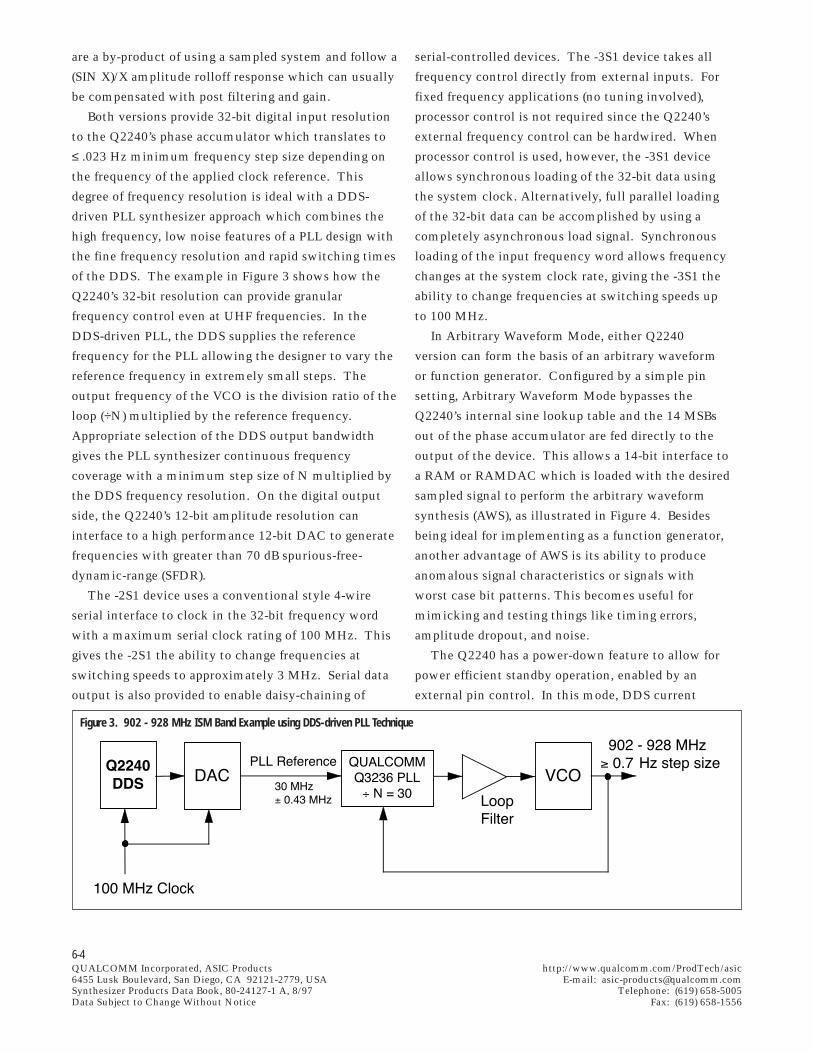
6-4QUALCOMM Incorporated, ASIC Products http://www.qualcomm.com/ProdTech/asic6455 Lusk Boulevard, San Diego, CA 92121-2779, USA E-mail: [email protected] Products Data Book, 80-24127-1 A, 8/97 Telephone: (619) 658-5005Data Subject to Change Without Notice Fax: (619) 658-1556
serial-controlled devices. The -3S1 device takes all
frequency control directly from external inputs. For
fixed frequency applications (no tuning involved),
processor control is not required since the Q2240’s
external frequency control can be hardwired. When
processor control is used, however, the -3S1 device
allows synchronous loading of the 32-bit data using
the system clock. Alternatively, full parallel loading
of the 32-bit data can be accomplished by using a
completely asynchronous load signal. Synchronous
loading of the input frequency word allows frequency
changes at the system clock rate, giving the -3S1 the
ability to change frequencies at switching speeds up
to 100 MHz.
In Arbitrary Waveform Mode, either Q2240
version can form the basis of an arbitrary waveform
or function generator. Configured by a simple pin
setting, Arbitrary Waveform Mode bypasses the
Q2240’s internal sine lookup table and the 14 MSBs
out of the phase accumulator are fed directly to the
output of the device. This allows a 14-bit interface to
a RAM or RAMDAC which is loaded with the desired
sampled signal to perform the arbitrary waveform
synthesis (AWS), as illustrated in Figure 4. Besides
being ideal for implementing as a function generator,
another advantage of AWS is its ability to produce
anomalous signal characteristics or signals with
worst case bit patterns. This becomes useful for
mimicking and testing things like timing errors,
amplitude dropout, and noise.
The Q2240 has a power-down feature to allow for
power efficient standby operation, enabled by an
external pin control. In this mode, DDS current
are a by-product of using a sampled system and follow a
(SIN X)/X amplitude rolloff response which can usually
be compensated with post filtering and gain.
Both versions provide 32-bit digital input resolution
to the Q2240’s phase accumulator which translates to
≤ .023 Hz minimum frequency step size depending on
the frequency of the applied clock reference. This
degree of frequency resolution is ideal with a DDS-
driven PLL synthesizer approach which combines the
high frequency, low noise features of a PLL design with
the fine frequency resolution and rapid switching times
of the DDS. The example in Figure 3 shows how the
Q2240’s 32-bit resolution can provide granular
frequency control even at UHF frequencies. In the
DDS-driven PLL, the DDS supplies the reference
frequency for the PLL allowing the designer to vary the
reference frequency in extremely small steps. The
output frequency of the VCO is the division ratio of the
loop (÷N) multiplied by the reference frequency.
Appropriate selection of the DDS output bandwidth
gives the PLL synthesizer continuous frequency
coverage with a minimum step size of N multiplied by
the DDS frequency resolution. On the digital output
side, the Q2240’s 12-bit amplitude resolution can
interface to a high performance 12-bit DAC to generate
frequencies with greater than 70 dB spurious-free-
dynamic-range (SFDR).
The -2S1 device uses a conventional style 4-wire
serial interface to clock in the 32-bit frequency word
with a maximum serial clock rating of 100 MHz. This
gives the -2S1 the ability to change frequencies at
switching speeds to approximately 3 MHz. Serial data
output is also provided to enable daisy-chaining of
Figure 3. 902 - 928 MHz ISM Band Example using DDS-driven PLL Technique
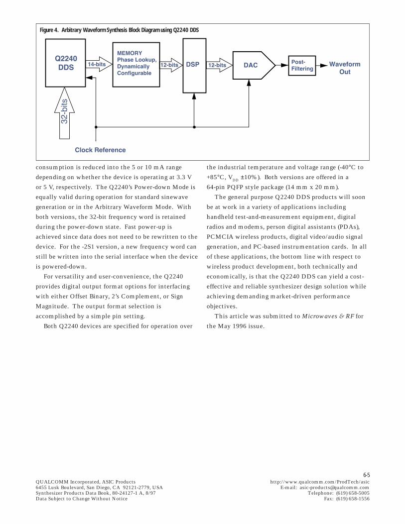
6-5QUALCOMM Incorporated, ASIC Products http://www.qualcomm.com/ProdTech/asic6455 Lusk Boulevard, San Diego, CA 92121-2779, USA E-mail: [email protected] Products Data Book, 80-24127-1 A, 8/97 Telephone: (619) 658-5005Data Subject to Change Without Notice Fax: (619) 658-1556
Figure 4. Arbitrary Waveform Synthesis Block Diagram using Q2240 DDS
consumption is reduced into the 5 or 10 mA range
depending on whether the device is operating at 3.3 V
or 5 V, respectively. The Q2240’s Power-down Mode is
equally valid during operation for standard sinewave
generation or in the Arbitrary Waveform Mode. With
both versions, the 32-bit frequency word is retained
during the power-down state. Fast power-up is
achieved since data does not need to be rewritten to the
device. For the -2S1 version, a new frequency word can
still be written into the serial interface when the device
is powered-down.
For versatility and user-convenience, the Q2240
provides digital output format options for interfacing
with either Offset Binary, 2’s Complement, or Sign
Magnitude. The output format selection is
accomplished by a simple pin setting.
Both Q2240 devices are specified for operation over
the industrial temperature and voltage range (-40°C to
+85°C, VDD ±10%). Both versions are offered in a
64-pin PQFP style package (14 mm x 20 mm).
The general purpose Q2240 DDS products will soon
be at work in a variety of applications including
handheld test-and-measurement equipment, digital
radios and modems, person digital assistants (PDAs),
PCMCIA wireless products, digital video/audio signal
generation, and PC-based instrumentation cards. In all
of these applications, the bottom line with respect to
wireless product development, both technically and
economically, is that the Q2240 DDS can yield a cost-
effective and reliable synthesizer design solution while
achieving demanding market-driven performance
objectives.
This article was submitted to Microwaves & RF for
the May 1996 issue.
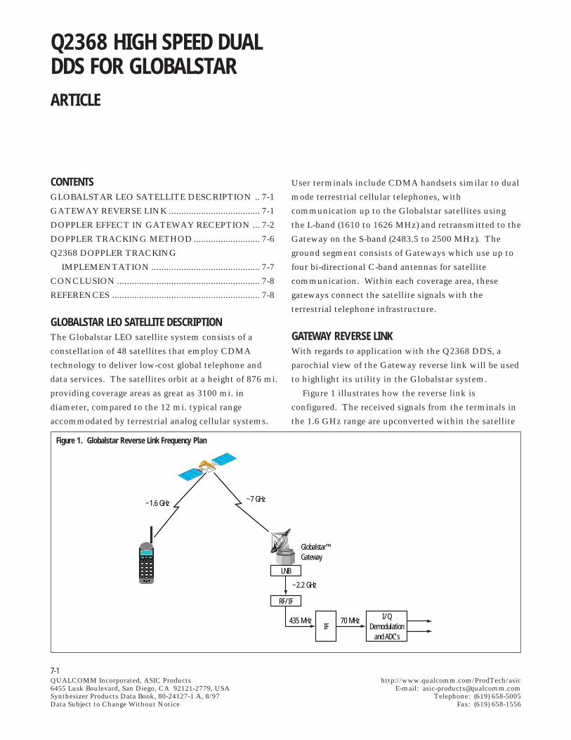
7-1QUALCOMM Incorporated, ASIC Products http://www.qualcomm.com/ProdTech/asic6455 Lusk Boulevard, San Diego, CA 92121-2779, USA E-mail: [email protected] Products Data Book, 80-24127-1 A, 8/97 Telephone: (619) 658-5005Data Subject to Change Without Notice Fax: (619) 658-1556
Q2368 HIGH SPEED DUALDDS FOR GLOBALSTARARTICLE
User terminals include CDMA handsets similar to dual
mode terrestrial cellular telephones, with
communication up to the Globalstar satellites using
the L-band (1610 to 1626 MHz) and retransmitted to the
Gateway on the S-band (2483.5 to 2500 MHz). The
ground segment consists of Gateways which use up to
four bi-directional C-band antennas for satellite
communication. Within each coverage area, these
gateways connect the satellite signals with the
terrestrial telephone infrastructure.
GATEWAY REVERSE LINKWith regards to application with the Q2368 DDS, a
parochial view of the Gateway reverse link will be used
to highlight its utility in the Globalstar system.
Figure 1 illustrates how the reverse link is
configured. The received signals from the terminals in
the 1.6 GHz range are upconverted within the satellite
Figure 1. Globalstar Reverse Link Frequency Plan
~1.6 GHz ~7 GHz
Globalstar™Gateway
~2.2 GHz
435 MHz 70 MHz
LNB
RF/IF
IFI/Q
Demodulationand ADC's
GLOBALSTAR LEO SATELLITE DESCRIPTIONThe Globalstar LEO satellite system consists of a
constellation of 48 satellites that employ CDMA
technology to deliver low-cost global telephone and
data services. The satellites orbit at a height of 876 mi.
providing coverage areas as great as 3100 mi. in
diameter, compared to the 12 mi. typical range
accommodated by terrestrial analog cellular systems.
CONTENTSGLOBALSTAR LEO SATELLITE DESCRIPTION .. 7-1
GATEWAY REVERSE LINK ..................................... 7-1
DOPPLER EFFECT IN GATEWAY RECEPTION ... 7-2
DOPPLER TRACKING METHOD........................... 7-6
Q2368 DOPPLER TRACKING
IMPLEMENTATION ............................................ 7-7
CONCLUSION .......................................................... 7-8
REFERENCES ............................................................ 7-8
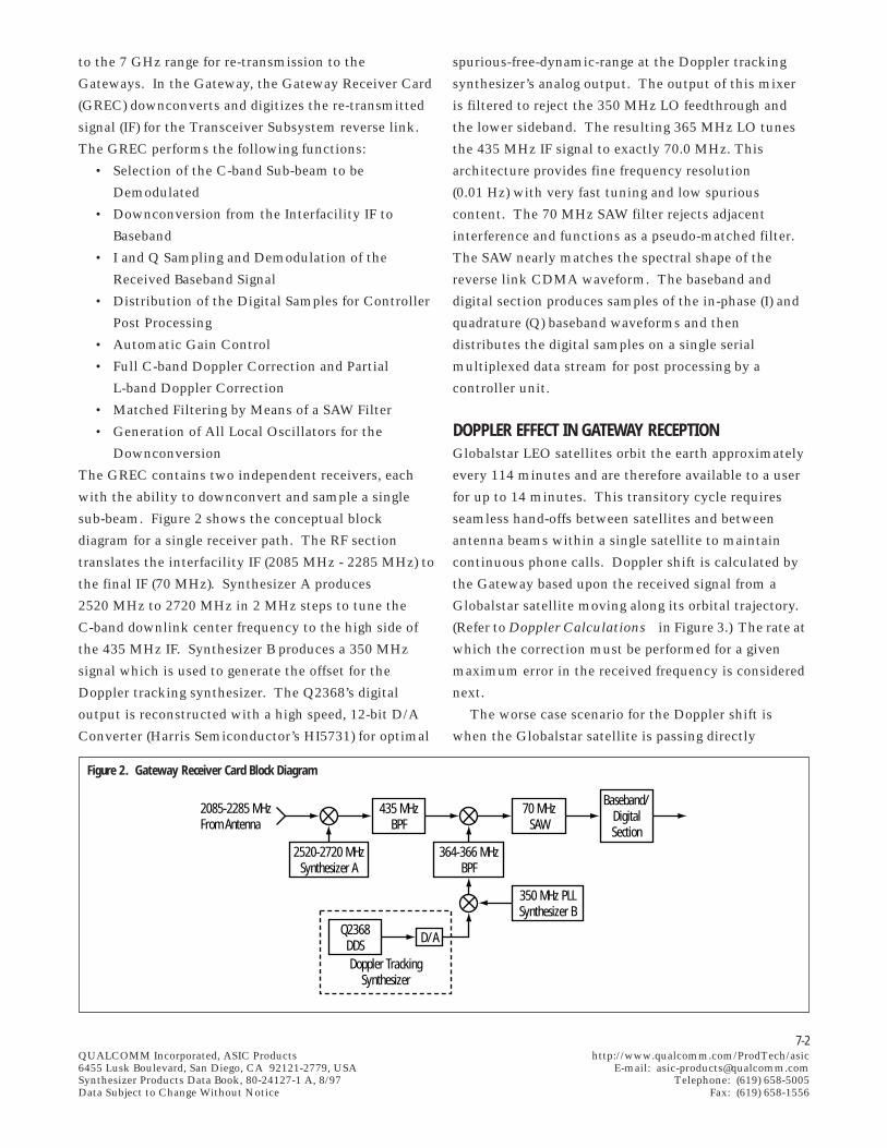
7-2QUALCOMM Incorporated, ASIC Products http://www.qualcomm.com/ProdTech/asic6455 Lusk Boulevard, San Diego, CA 92121-2779, USA E-mail: [email protected] Products Data Book, 80-24127-1 A, 8/97 Telephone: (619) 658-5005Data Subject to Change Without Notice Fax: (619) 658-1556
to the 7 GHz range for re-transmission to the
Gateways. In the Gateway, the Gateway Receiver Card
(GREC) downconverts and digitizes the re-transmitted
signal (IF) for the Transceiver Subsystem reverse link.
The GREC performs the following functions:
• Selection of the C-band Sub-beam to be
Demodulated
• Downconversion from the Interfacility IF to
Baseband
• I and Q Sampling and Demodulation of the
Received Baseband Signal
• Distribution of the Digital Samples for Controller
Post Processing
• Automatic Gain Control
• Full C-band Doppler Correction and Partial
L-band Doppler Correction
• Matched Filtering by Means of a SAW Filter
• Generation of All Local Oscillators for the
Downconversion
The GREC contains two independent receivers, each
with the ability to downconvert and sample a single
sub-beam. Figure 2 shows the conceptual block
diagram for a single receiver path. The RF section
translates the interfacility IF (2085 MHz - 2285 MHz) to
the final IF (70 MHz). Synthesizer A produces
2520 MHz to 2720 MHz in 2 MHz steps to tune the
C-band downlink center frequency to the high side of
the 435 MHz IF. Synthesizer B produces a 350 MHz
signal which is used to generate the offset for the
Doppler tracking synthesizer. The Q2368’s digital
output is reconstructed with a high speed, 12-bit D/A
Converter (Harris Semiconductor’s HI5731) for optimal
spurious-free-dynamic-range at the Doppler tracking
synthesizer’s analog output. The output of this mixer
is filtered to reject the 350 MHz LO feedthrough and
the lower sideband. The resulting 365 MHz LO tunes
the 435 MHz IF signal to exactly 70.0 MHz. This
architecture provides fine frequency resolution
(0.01 Hz) with very fast tuning and low spurious
content. The 70 MHz SAW filter rejects adjacent
interference and functions as a pseudo-matched filter.
The SAW nearly matches the spectral shape of the
reverse link CDMA waveform. The baseband and
digital section produces samples of the in-phase (I) and
quadrature (Q) baseband waveforms and then
distributes the digital samples on a single serial
multiplexed data stream for post processing by a
controller unit.
DOPPLER EFFECT IN GATEWAY RECEPTIONGlobalstar LEO satellites orbit the earth approximately
every 114 minutes and are therefore available to a user
for up to 14 minutes. This transitory cycle requires
seamless hand-offs between satellites and between
antenna beams within a single satellite to maintain
continuous phone calls. Doppler shift is calculated by
the Gateway based upon the received signal from a
Globalstar satellite moving along its orbital trajectory.
(Refer to Doppler Calculations in Figure 3.) The rate at
which the correction must be performed for a given
maximum error in the received frequency is considered
next.
The worse case scenario for the Doppler shift is
when the Globalstar satellite is passing directly
Figure 2. Gateway Receiver Card Block Diagram
2520-2720 MHzSynthesizer A
2085-2285 MHzFrom Antenna
435 MHzBPF
70 MHzSAW
Baseband/DigitalSection
364-366 MHzBPF
350 MHz PLLSynthesizer B
Q2368DDS D/A
Doppler TrackingSynthesizer
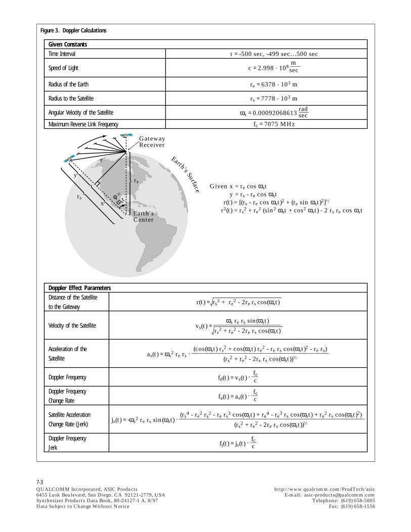
7-3QUALCOMM Incorporated, ASIC Products http://www.qualcomm.com/ProdTech/asic6455 Lusk Boulevard, San Diego, CA 92121-2779, USA E-mail: [email protected] Products Data Book, 80-24127-1 A, 8/97 Telephone: (619) 658-5005Data Subject to Change Without Notice Fax: (619) 658-1556
Figure 3. Doppler Calculations
Given ConstantsTime Interval
Speed of Light
Radius of the Earth
Radius to the Satellite
Angular Velocity of the Satellite
Maximum Reverse Link Frequency
t = -500 sec, -499 sec…500 sec
c = 2.998 . 108 –––
ωs = 0.00092068613 –––
fc = 7075 MHz
re = 6378 . 103 m
rs = 7778 . 103 m
Doppler Effect ParametersDistance of the Satelliteto the Gateway
Velocity of the Satellite
Acceleration of theSatellite
Doppler Frequency
Doppler FrequencyChange Rate
Satellite AccelerationChange Rate (Jerk)
Doppler FrequencyJerk
r(t) = rs2 + re
2 - 2re rs cos(ωst)
vs(t) = –––––––––––––––––––––
as(t) = ωs2 re rs . –––––––––––––––––––––––––––––––––––––––––––
js(t) = -ωs2 re rs sin(ωst) . ––––––––––––––––––––––––––––––––––––––––––––––––––––––––––
fd(t) = vs(t) . ––
fa(t) = as(t) . ––
fj(t) = js(t) . ––
msec
radsec
ωs re rs sin(ωst)
rs2 + re
2 - 2re rs cos(ωst)
(cos(ωst) rs2 + cos(ωst) re
2 - re rs cos(ωst)2 - re rs)
(rs2 + re
2 - 2re rs cos(ωst))3⁄2
(rs4 - re
2 rs2 - re rs
3 cos(ωst) + re4 - re
3 rs cos(ωst) + re2 rs cos(ωst)2)
(rs2 + re
2 - 2re rs cos(ωst))5⁄2
fcc
fcc
fcc
Given x = re cos ωst y = rs - re cos ωst
r(t) = [(rs - re cos ωst)2 + (re sin ωst)2]1⁄2
r2(t) = rs2 + re
2 (sin2 ωst + cos2 ωst) - 2 rs re cos ωst
r
y
xrs
re
φ =ω st
GatewayReceiver
Earth's SurfaceEarth'sCenter
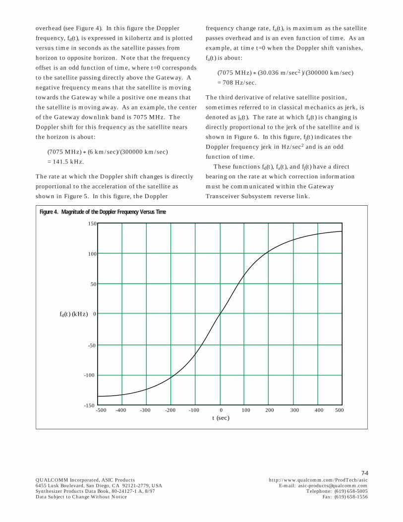
7-4QUALCOMM Incorporated, ASIC Products http://www.qualcomm.com/ProdTech/asic6455 Lusk Boulevard, San Diego, CA 92121-2779, USA E-mail: [email protected] Products Data Book, 80-24127-1 A, 8/97 Telephone: (619) 658-5005Data Subject to Change Without Notice Fax: (619) 658-1556
overhead (see Figure 4). In this figure the Doppler
frequency, fd(t), is expressed in kilohertz and is plotted
versus time in seconds as the satellite passes from
horizon to opposite horizon. Note that the frequency
offset is an odd function of time, where t=0 corresponds
to the satellite passing directly above the Gateway. A
negative frequency means that the satellite is moving
towards the Gateway while a positive one means that
the satellite is moving away. As an example, the center
of the Gateway downlink band is 7075 MHz. The
Doppler shift for this frequency as the satellite nears
the horizon is about:
(7075 MHz) * (6 km/sec)/(300000 km/sec)
= 141.5 kHz.
The rate at which the Doppler shift changes is directly
proportional to the acceleration of the satellite as
shown in Figure 5. In this figure, the Doppler
frequency change rate, fa(t), is maximum as the satellite
passes overhead and is an even function of time. As an
example, at time t=0 when the Doppler shift vanishes,
fa(t) is about:
(7075 MHz) * (30.036 m/sec2 )/(300000 km/sec)
= 708 Hz/sec.
The third derivative of relative satellite position,
sometimes referred to in classical mechanics as jerk, is
denoted as js(t). The rate at which fa(t) is changing is
directly proportional to the jerk of the satellite and is
shown in Figure 6. In this figure, fj(t) indicates the
Doppler frequency jerk in Hz/sec2 and is an odd
function of time.
These functions fd(t), fa(t), and fj(t) have a direct
bearing on the rate at which correction information
must be communicated within the Gateway
Transceiver Subsystem reverse link.
Figure 4. Magnitude of the Doppler Frequency Versus Time
-500 -400 -300 -200 -100 0 100 200 300 400 500-150
-100
-50
0
50
100
150
t (sec)
fd(t) (kHz)
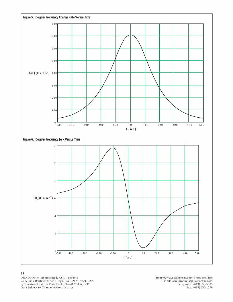
7-5QUALCOMM Incorporated, ASIC Products http://www.qualcomm.com/ProdTech/asic6455 Lusk Boulevard, San Diego, CA 92121-2779, USA E-mail: [email protected] Products Data Book, 80-24127-1 A, 8/97 Telephone: (619) 658-5005Data Subject to Change Without Notice Fax: (619) 658-1556
Figure 5. Doppler Frequency Change Rate Versus Time
-500 -300 -200 -100 0 100 200 300 400 5000
100
200
300
400
500
600
700
800
-400
fa(t) (Hz/sec)
t (sec)
Figure 6. Doppler Frequency Jerk Versus Time
-500 -400 -300 -200 -100 0 100 200 300 400 500-3
-2
-1
0
1
2
3
t (sec)
fj(t) (Hz/sec2)
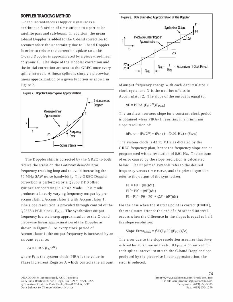
7-6QUALCOMM Incorporated, ASIC Products http://www.qualcomm.com/ProdTech/asic6455 Lusk Boulevard, San Diego, CA 92121-2779, USA E-mail: [email protected] Products Data Book, 80-24127-1 A, 8/97 Telephone: (619) 658-5005Data Subject to Change Without Notice Fax: (619) 658-1556
DOPPLER TRACKING METHODC-band instantaneous Doppler signature is a
continuous function of time unique to a particular
satellite pass and sub-beam. In addition, the mean
L-band Doppler is added to the C-band correction to
accommodate the uncertainty due to L-band Doppler.
In order to reduce the correction update rate, the
C-band Doppler is approximated by a piecewise-linear
polynomial. The slope of the Doppler correction and
the initial correction are sent to the GREC once every
spline interval. A linear spline is simply a piecewise
linear approximation to a given function as shown in
Figure 7. of output frequency change with each Accumulator 1
clock cycle, and N is the number of bits in
Accumulator 2. The slope of the output is equal to:
∆F = PIRA (FS/2N)(FPCR)
The smallest non-zero slope for a constant clock period
is obtained when PIRA=1, resulting in a minimum
slope resolution of:
∆FMIN = (FS/2N) * (FPCR) = (0.01 Hz) * (FPCR)
The system clock is 43.75 MHz as dictated by the
GREC frequency plan, hence the frequency slope can be
programmed with a resolution of 0.01 Hz. The amount
of error caused by the slope resolution is calculated
below. The unprimed symbols refer to the desired
frequency versus time curve, and the primed symbols
refer to the output of the synthesizer.
F1 = F0 + (∆F)(∆t)
F1´= F0´ + (∆F´)(∆t)
F1 - F1´= F0 - F0´ + (∆F - ∆F´)(∆t)
For the case when the starting point is correct (F0=F0´),
the maximum error at the end of a ∆t second interval
occurs when the difference in the slopes is equal to half
the slope resolution:
Slope ErrorMAX = (1⁄2)(FS/2N)(FPCR)(∆t)
The error due to the slope resolution assumes that FPCR
is fixed for all spline intervals. If FPCR is optimized for
each spline interval to match the C-band Doppler slope
produced by the piecewise-linear approximation, the
error is reduced.
Figure 8. DDS Stair-step Approximation of the Doppler
∆F
F0
F1
F0'
F
t
F1'
TPCR
∆s
Synthesizer Output
Piecewise-Linear DopplerApproximation
TPCR = = Accumulator 1 Clock Period1FPCR
Figure 7. Doppler Linear Spline Approximation
InstantaneousDoppler
Piecewise-linearApproximation
F
t FrequencyErrorF0
F1
Spline Interval
The Doppler shift is corrected by the GREC to both
reduce the stress on the Gateway demodulator
frequency tracking loop and to avoid increasing the
70 MHz SAW noise bandwidth. The GREC Doppler
correction is performed by a Q2368 DDS offset
synthesizer operating in Chirp Mode. This mode
produces a linearly varying frequency output by pre-
accumulating Accumulator 2 with Accumulator 1.
Fine slope resolution is provided through control of the
Q2368’s PCR clock, FPCR. The synthesizer output
frequency is a stair-step approximation to the C-band
piecewise linear approximation of the Doppler as
shown in Figure 8. At every clock period of
Accumulator 1, the output frequency is increased by an
amount equal to:
∆s = PIRA (FS/2N)
where FS is the system clock, PIRA is the value in
Phase Increment Register A which controls the amount
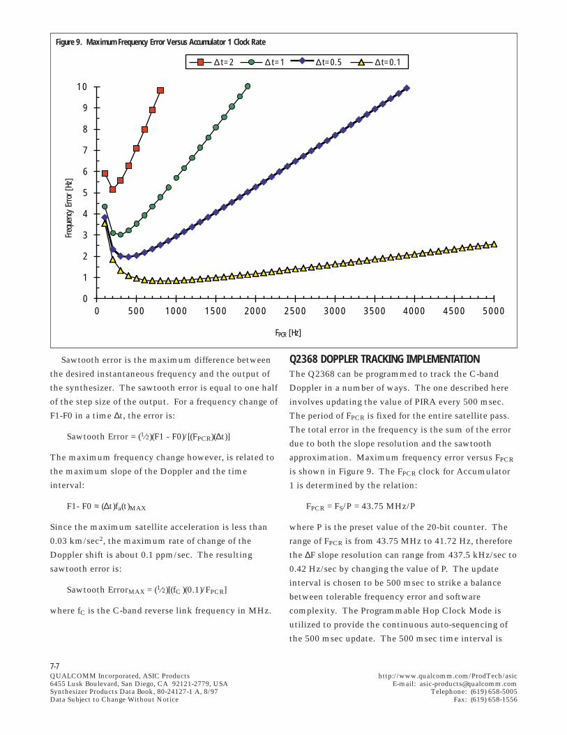
7-7QUALCOMM Incorporated, ASIC Products http://www.qualcomm.com/ProdTech/asic6455 Lusk Boulevard, San Diego, CA 92121-2779, USA E-mail: [email protected] Products Data Book, 80-24127-1 A, 8/97 Telephone: (619) 658-5005Data Subject to Change Without Notice Fax: (619) 658-1556
Figure 9. Maximum Frequency Error Versus Accumulator 1 Clock Rate
Sawtooth error is the maximum difference between
the desired instantaneous frequency and the output of
the synthesizer. The sawtooth error is equal to one half
of the step size of the output. For a frequency change of
F1-F0 in a time ∆t, the error is:
Sawtooth Error = (1⁄2)(F1 - F0)/[(FPCR)(∆t)]
The maximum frequency change however, is related to
the maximum slope of the Doppler and the time
interval:
F1- F0 ≈ (∆t)fa(t)MAX
Since the maximum satellite acceleration is less than
0.03 km/sec2, the maximum rate of change of the
Doppler shift is about 0.1 ppm/sec. The resulting
sawtooth error is:
Sawtooth ErrorMAX = (1⁄2)[(fC )(0.1)/FPCR]
where fC is the C-band reverse link frequency in MHz.
Q2368 DOPPLER TRACKING IMPLEMENTATIONThe Q2368 can be programmed to track the C-band
Doppler in a number of ways. The one described here
involves updating the value of PIRA every 500 msec.
The period of FPCR is fixed for the entire satellite pass.
The total error in the frequency is the sum of the error
due to both the slope resolution and the sawtooth
approximation. Maximum frequency error versus FPCR
is shown in Figure 9. The FPCR clock for Accumulator
1 is determined by the relation:
FPCR = FS/P = 43.75 MHz/P
where P is the preset value of the 20-bit counter. The
range of FPCR is from 43.75 MHz to 41.72 Hz, therefore
the ∆F slope resolution can range from 437.5 kHz/sec to
0.42 Hz/sec by changing the value of P. The update
interval is chosen to be 500 msec to strike a balance
between tolerable frequency error and software
complexity. The Programmable Hop Clock Mode is
utilized to provide the continuous auto-sequencing of
the 500 msec update. The 500 msec time interval is
0
1
2
3
4
5
6
7
8
9
1 0
0 5 0 0 1 0 0 0 1 5 0 0 2 0 0 0 2 5 0 0 3 0 0 0 3 5 0 0 4 0 0 0 4 5 0 0 5 0 0 0
FPCR [Hz]
Freq
uenc
y Er
ror [
Hz]
∆ t = 2 ∆ t = 1 ∆ t=0 .5 ∆ t=0 .1
7-8QUALCOMM Incorporated, ASIC Products http://www.qualcomm.com/ProdTech/asic6455 Lusk Boulevard, San Diego, CA 92121-2779, USA E-mail: [email protected] Products Data Book, 80-24127-1 A, 8/97 Telephone: (619) 658-5005Data Subject to Change Without Notice Fax: (619) 658-1556
produced by programming the 32-bit PHC counter with
a divide value of 21,875,000. FPCR is selected to be
400 Hz to minimize frequency error with the chosen
500 msec update interval and is produced by
programming P with a divide value of 109,375. Exactly
200 cycles of the FPCR occur during each spline interval.
The frequency slope resolution is 4 Hz/sec and the
tracking error is bounded at 2 Hz with the selected
implementation.
The Gateway Transceiver Subsystem software
updates the DDS slope value every spline interval. In
order to maintain phase continuity, the initial
frequency is not updated every interval. Because of the
limited slope resolution of the Q2368, there may exist a
residual frequency error as large as 1 Hz which carries
over into the next spline interval. In order to keep this
error from growing, the software selects the slope for
interval j that minimizes the instantaneous frequency
error at the end of interval j based on the following
criteria:
1. Residual Error of Interval j-1
2. Desired Slope for Interval j
3. Under the Constraint that the Frequency Slope
Resolution is 4 Hz/sec.
The following example will be used to clarify this. The
desired slope for interval #1 is 18 Hz/sec and the initial
frequency is 100 Hz. The Q2368 is programmed to
generate a slope of 20 Hz/sec from an initial 100 Hz
frequency. At the end of the first 500 msec interval,
the DDS output is 110 Hz, or 1 Hz too high. The
desired slope for interval #2 is 19 Hz/sec. The software
has the option of generating a slope of 16 Hz/sec or
20 Hz/sec. In order to reduce the error at the end of
interval #2, the Q2368 is programmed to produce a
slope of 16 Hz/sec. At the end of interval #2, the DDS
output is less than the desired output by 0.5 Hz.
CONCLUSIONThe Q2368 Dual DDS offers a high-utility design
solution for frequency synthesis in digital wireless
communications. In the Globalstar LEOSAT system, a
method has been described for using the Q2368 to
correct the Gateway reception for the Doppler effect.
Since the rate of the Doppler shift varies numerically
slower as a function of time than the Doppler shift
itself, the time intervals between updates on the rate of
change of Doppler can be much greater for the same
error in transmitted frequency than the time intervals
required between updates of the absolute Doppler shift.
This is equivalent to approximating the Doppler
frequency as a function of time with a piecewise-linear
polynomial. Therefore, the CPU controlling the Q2368
needs to provide only the rate of change of Doppler
frequency as opposed to a new Doppler frequency
correction for each time instant.
REFERENCES1. Description of the Globalstar System,
QUALCOMM, Inc., 1994
2. QUALCOMM, S. Mollenkopf/J. Zegarra internal
notes, Globalstar Gateway Receiver Card.
3. QUALCOMM, R. Kaufman/J. Lorbeck private
notes, Globalstar Doppler correction.
This section is excerpted from an article that was
submitted to RF Design for the May 1996 Issue.
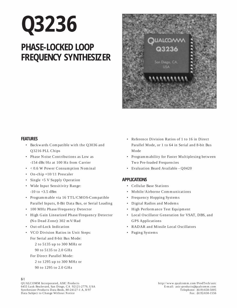
8-1QUALCOMM Incorporated, ASIC Products http://www.qualcomm.com/ProdTech/asic6455 Lusk Boulevard, San Diego, CA 92121-2779, USA E-mail: [email protected] Products Data Book, 80-24127-1 A, 8/97 Telephone: (619) 658-5005Data Subject to Change Without Notice Fax: (619) 658-1556
Q3236PHASE-LOCKED LOOPFREQUENCY SYNTHESIZER
FEATURES• Backwards Compatible with the Q3036 and
Q3216 PLL Chips
• Phase Noise Contributions as Low as
-154 dBc/Hz at 100 Hz from Carrier
• < 0.6 W Power Consumption Nominal
• On-chip ÷10/11 Prescaler
• Single +5 V Supply Operation
• Wide Input Sensitivity Range:
-10 to +3.5 dBm
• Programmable via 16 TTL/CMOS-Compatible
Parallel Inputs, 8-Bit Data Bus, or Serial Loading
• 100 MHz Phase/Frequency Detector
• High Gain Linearized Phase/Frequency Detector
(No Dead Zone): 302 mV/Rad
• Out-of-Lock Indication
• VCO Division Ratios in Unit Steps:
For Serial and 8-bit Bus Mode:
2 to 5135 up to 300 MHz or
90 to 5135 to 2.0 GHz
For Direct Parallel Mode:
2 to 1295 up to 300 MHz or
90 to 1295 to 2.0 GHz
• Reference Division Ratios of 1 to 16 in Direct
Parallel Mode, or 1 to 64 in Serial and 8-bit Bus
Mode
• Programmability for Faster Multiplexing between
Two Pre-loaded Frequencies
• Evaluation Board Available - Q0420
APPLICATIONS• Cellular Base Stations
• Mobile/Airborne Communications
• Frequency Hopping Systems
• Digital Radios and Modems
• High Performance Test Equipment
• Local Oscillator Generation for VSAT, DBS, and
GPS Applications
• RADAR and Missile Local Oscillators
• Paging Systems
8-2QUALCOMM Incorporated, ASIC Products http://www.qualcomm.com/ProdTech/asic6455 Lusk Boulevard, San Diego, CA 92121-2779, USA E-mail: [email protected] Products Data Book, 80-24127-1 A, 8/97 Telephone: (619) 658-5005Data Subject to Change Without Notice Fax: (619) 658-1556
CONTENTSGENERAL DESCRIPTION ........................................................................................................................................... 8-4
FUNCTIONAL OVERVIEW ......................................................................................................................................... 8-5
Differential Line Receivers .................................................................................................................................. 8-5
VCO Divider ......................................................................................................................................................... 8-6
Reference Divider ................................................................................................................................................. 8-7
Digital Phase/Frequency Detector ....................................................................................................................... 8-7
Digital Processor Interface (DPI) Modes .............................................................................................................. 8-8
Enhanced Operation or Q3036 Mode ......................................................................................................... 8-9
Direct Parallel Input Mode ......................................................................................................................... 8-9
8-bit Bus Mode ............................................................................................................................................. 8-9
Serial Bus Mode ........................................................................................................................................... 8-9
8-bit Bus or Serial Bus Frequency Multiplexing: Ping-Pong Mode ....................................................... 8-10
TECHNICAL SPECIFICATIONS ............................................................................................................................... 8-12
INPUT/OUTPUT SIGNALS ....................................................................................................................................... 8-17
APPLICATION INFORMATION............................................................................................................................... 8-21
General ................................................................................................................................................................ 8-21
VCO/Reference Input Connections ................................................................................................................... 8-21
Programming the Binary Counters .................................................................................................................... 8-21
Calculating Loop Filter Component Values ..................................................................................................... 8-21
Loop Stability Analysis ...................................................................................................................................... 8-22
Op Amp Finite Gain/Bandwidth ....................................................................................................................... 8-23
Pre-Integrator Filtering ....................................................................................................................................... 8-23
Digital Phase Detector Sampling Delay ............................................................................................................ 8-24
Additional Reference Suppression Filtering ...................................................................................................... 8-24
Stability Analysis (Revisited) and Closed Loop Response ................................................................................ 8-26
Synthesizer Output Spectrum ........................................................................................................................... 8-29
FREQUENCY SYNTHESIZER DESIGN CONSIDERATIONS WITH THE Q3236 ................................................ 8-30
General Electromagnetic Issues ......................................................................................................................... 8-30
VCO And Reference Line Receiver Input Minimum Edge Rates .................................................................... 8-31
Phase/Frequency Detector Considerations ....................................................................................................... 8-32
Phase Noise Performance Considerations ........................................................................................................ 8-33
Settling Time Considerations ............................................................................................................................ 8-36
Using External Prescalers for Higher Frequency Translation .......................................................................... 8-36
Q3036 TO Q3236 MIGRATION ................................................................................................................................ 8-39
Q0420 PLO EVALUATION SYSTEM ........................................................................................................................ 8-40
PLCC PACKAGING.................................................................................................................................................... 8-42
RECOMMENDED SOCKETS..................................................................................................................................... 8-43
REFERENCES .............................................................................................................................................................. 8-43
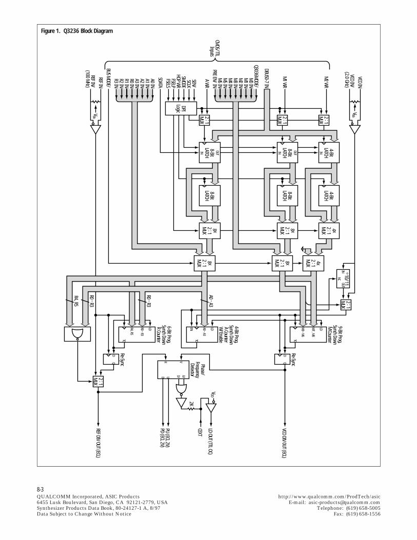
8-3QUALCOMM Incorporated, ASIC Products http://www.qualcomm.com/ProdTech/asic6455 Lusk Boulevard, San Diego, CA 92121-2779, USA E-mail: [email protected] Products Data Book, 80-24127-1 A, 8/97 Telephone: (619) 658-5005Data Subject to Change Without Notice Fax: (619) 658-1556
VbbVCO IN
VCO IN/(2.0 GHz)
M2 WR
M1 WR
DBUS0-7 IN
Q3036MODE/M0 INM1 INM2 INM3 INM4 INM5 INM6 IN
PRE EN/ IN
A WR
SEN/SCLK
SMODEHOP W
RFSELPFSELS
SDATA
A0 INA1 INA2 INA3 INR0 INR1 INR2 INR3 IN
BUS MODE/
REF IN
REF IN/(100 MHz)
Vbb 2 : 1MUX
4-BitLATCH
4 x2 : 1MUX
2 : 1MUX
8-BitLATCH
8 x2 : 1MUX
8 x2 : 1MUX
8 x2 : 1MUX
2 : 1MUX
2 : 1MUX
2 : 1MUX
8-BitLATCH
8 x2 : 1MUX
4x2 : 1MUX
DPILogic
4-BitLATCH
8-BitLATCH
8-BitLATCH
DQ
OUT
IN INOUT
IN
INOUT
NC
÷10/119-Bit Prog.Synch DownM Counter
4-Bit Prog.Synch DownA CounterW
/Enable
6-Bit Prog.Synch DownR Counter
LDM7 , M8
M0 - M6
LDA0 - A3
ENLDR0 - R3
R4, R5
TCTCTC
DQ
Re-Sync
Re-SyncVR
U/D/UD
Phase/FrequencyDetector
VCO DIV 0UT (ECL)
LD OUT (TTL OC)
CEXT
PU (ECL 2V)PD (ECL 2V)
REF DIV OUT (ECL)
2K
VDDA0 - A3
R0 - R3
R0 - R3
R4, R5
CMOS/TTLInputs
Figure 1. Q3236 Block Diagram
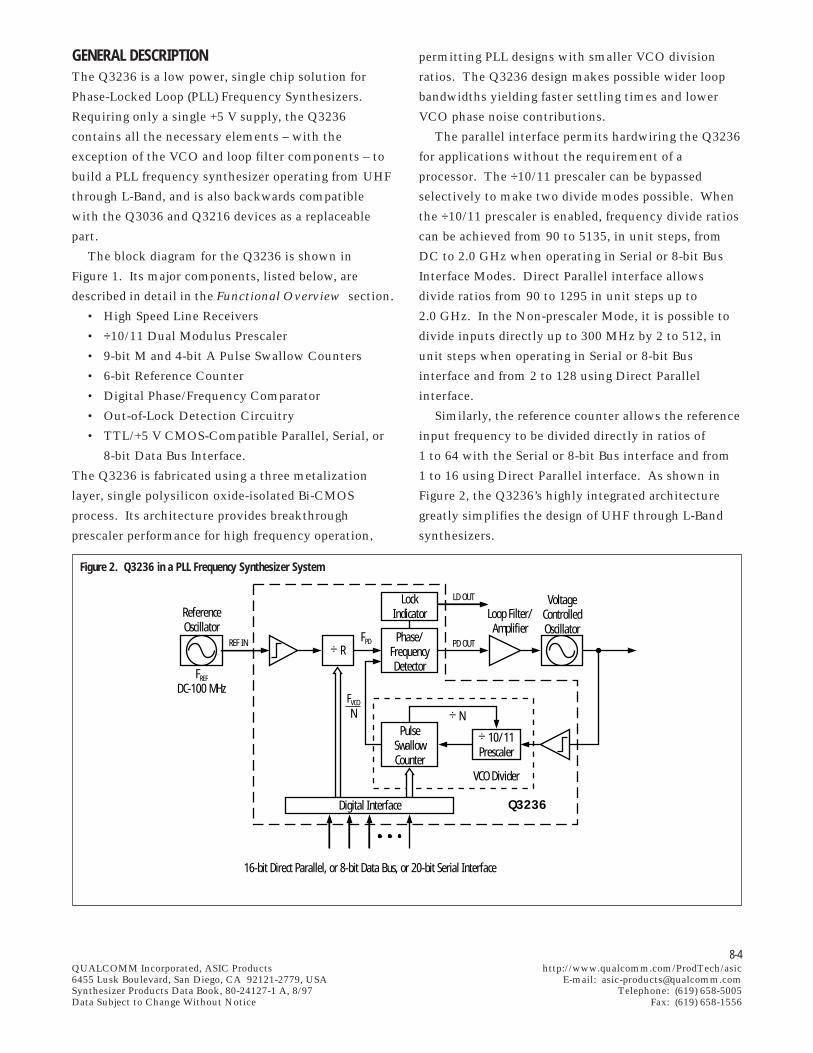
8-4QUALCOMM Incorporated, ASIC Products http://www.qualcomm.com/ProdTech/asic6455 Lusk Boulevard, San Diego, CA 92121-2779, USA E-mail: [email protected] Products Data Book, 80-24127-1 A, 8/97 Telephone: (619) 658-5005Data Subject to Change Without Notice Fax: (619) 658-1556
permitting PLL designs with smaller VCO division
ratios. The Q3236 design makes possible wider loop
bandwidths yielding faster settling times and lower
VCO phase noise contributions.
The parallel interface permits hardwiring the Q3236
for applications without the requirement of a
processor. The ÷10/11 prescaler can be bypassed
selectively to make two divide modes possible. When
the ÷10/11 prescaler is enabled, frequency divide ratios
can be achieved from 90 to 5135, in unit steps, from
DC to 2.0 GHz when operating in Serial or 8-bit Bus
Interface Modes. Direct Parallel interface allows
divide ratios from 90 to 1295 in unit steps up to
2.0 GHz. In the Non-prescaler Mode, it is possible to
divide inputs directly up to 300 MHz by 2 to 512, in
unit steps when operating in Serial or 8-bit Bus
interface and from 2 to 128 using Direct Parallel
interface.
Similarly, the reference counter allows the reference
input frequency to be divided directly in ratios of
1 to 64 with the Serial or 8-bit Bus interface and from
1 to 16 using Direct Parallel interface. As shown in
Figure 2, the Q3236’s highly integrated architecture
greatly simplifies the design of UHF through L-Band
synthesizers.
GENERAL DESCRIPTIONThe Q3236 is a low power, single chip solution for
Phase-Locked Loop (PLL) Frequency Synthesizers.
Requiring only a single +5 V supply, the Q3236
contains all the necessary elements – with the
exception of the VCO and loop filter components – to
build a PLL frequency synthesizer operating from UHF
through L-Band, and is also backwards compatible
with the Q3036 and Q3216 devices as a replaceable
part.
The block diagram for the Q3236 is shown in
Figure 1. Its major components, listed below, are
described in detail in the Functional Overview section.
• High Speed Line Receivers
• ÷10/11 Dual Modulus Prescaler
• 9-bit M and 4-bit A Pulse Swallow Counters
• 6-bit Reference Counter
• Digital Phase/Frequency Comparator
• Out-of-Lock Detection Circuitry
• TTL/+5 V CMOS-Compatible Parallel, Serial, or
8-bit Data Bus Interface.
The Q3236 is fabricated using a three metalization
layer, single polysilicon oxide-isolated Bi-CMOS
process. Its architecture provides breakthrough
prescaler performance for high frequency operation,
Figure 2. Q3236 in a PLL Frequency Synthesizer System
PD OUT
LD OUTLockIndicator
Phase/FrequencyDetector
÷ R
Loop Filter/Amplifier
VoltageControlledOscillator
REF IN
FREF
DC-100 MHz
ReferenceOscillator
Digital Interface
÷ N
÷ 10/11Prescaler
PulseSwallowCounter
VCO Divider
FPD
FVCO
N
Q3236
16-bit Direct Parallel, or 8-bit Data Bus, or 20-bit Serial Interface
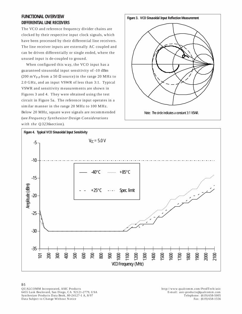
8-5QUALCOMM Incorporated, ASIC Products http://www.qualcomm.com/ProdTech/asic6455 Lusk Boulevard, San Diego, CA 92121-2779, USA E-mail: [email protected] Products Data Book, 80-24127-1 A, 8/97 Telephone: (619) 658-5005Data Subject to Change Without Notice Fax: (619) 658-1556
FUNCTIONAL OVERVIEWDIFFERENTIAL LINE RECEIVERSThe VCO and reference frequency divider chains are
clocked by their respective input clock signals, which
have been processed by their differential line receivers.
The line receiver inputs are externally AC coupled and
can be driven differentially or single ended, where the
unused input is de-coupled to ground.
When configured this way, the VCO input has a
guaranteed sinusoidal input sensitivity of -10 dBm
(200 mVP-P from a 50 Ω source) in the range 20 MHz to
2.0 GHz, and an input VSWR of less than 3:1. Typical
VSWR and sensitivity measurements are shown in
Figures 3 and 4. They were obtained using the test
circuit in Figure 5a. The reference input operates in a
similar manner in the range 20 MHz to 100 MHz.
Below 20 MHz, square wave signals are recommended
(see Frequency Synthesizer Design Considerations
with the Q3236 section).
Figure 4. Typical VCO Sinusoidal Input Sensitivity
Figure 3. VCO Sinusoidal Input Reflection Measurement
Note: The circle indicates a constant 3:1 VSWR.
101
200
300
400
500
600
700
800
900
1000
1100
1200
1300
1400
1500
1600
1700
1800
1900
2000
2100
-35
-30
-25
-20
-15
-10
-5
Ampli
tude
(dBm
)
VCO Frequency (MHz)
-40°C
+25°C
+85°C
Spec. limit
VCC = 5.0 V
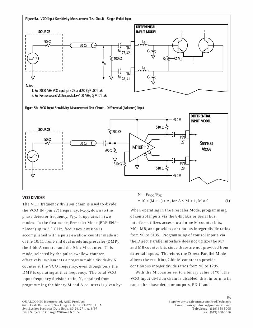
8-6QUALCOMM Incorporated, ASIC Products http://www.qualcomm.com/ProdTech/asic6455 Lusk Boulevard, San Diego, CA 92121-2779, USA E-mail: [email protected] Products Data Book, 80-24127-1 A, 8/97 Telephone: (619) 658-5005Data Subject to Change Without Notice Fax: (619) 658-1556
Figure 5a. VCO Input Sensitivity Measurement Test Circuit - Single-Ended Input
50 Ω
SOURCE
50 Ω
VIN
CS
CS
PIN27, 42
PIN28, 41 CP
LS
CP
LS
DIFFERENTIALINPUT MODEL
VbbRD100 Ω
Notes: 1. For 2000 MHz VCO input, pins 27 and 28, CS = .001 µF. 2. For Reference and VCO inputs below 100 MHz, CS = .01 µF.
Figure 5b. VCO Input Sensitivity Measurement Test Circuit - Differential (balanced) Input
50 Ω
SOURCE
50 ΩPIN27
PIN28
DIFFERENTIALINPUT MODEL
Same asAbove
200 Ω510 Ω
510 Ω
65 Ω
510 Ω
-5.2 V
-5.2 V
MC10E112
VCO DIVIDERThe VCO frequency division chain is used to divide
the VCO IN (pin 27) frequency, FVCO, down to the
phase detector frequency, FPD. It operates in two
modes. In the first mode, Prescaler Mode (PRE EN/ =
“Low”) up to 2.0 GHz, frequency division is
accomplished with a pulse-swallow counter made up
of the 10/11 front-end dual modulus prescaler (DMP),
the 4-bit A counter and the 9-bit M counter. This
mode, selected by the pulse-swallow counter,
effectively implements a programmable divide-by N
counter at the VCO frequency, even though only the
DMP is operating at that frequency. The total VCO
input frequency division ratio, N, obtained from
programming the binary M and A counters is given by:
N = FVCO/FPD
= 10 * (M + 1) + A, for A ≤ M + 1, M ≠ 0 (1)
When operating in the Prescaler Mode, programming
of control inputs via the 8-Bit Bus or Serial Bus
interface utilizes access to all nine M counter bits,
M0 - M8, and provides continuous integer divide ratios
from 90 to 5135. Programming of control inputs via
the Direct Parallel interface does not utilize the M7
and M8 counter bits since these are not provided from
external inputs. Therefore, the Direct Parallel Mode
allows the resulting 7-bit M counter to provide
continuous integer divide ratios from 90 to 1295.
With the M counter set to a binary value of “0”, the
VCO input division chain is disabled; this, in turn, will
cause the phase detector outputs, PD U and
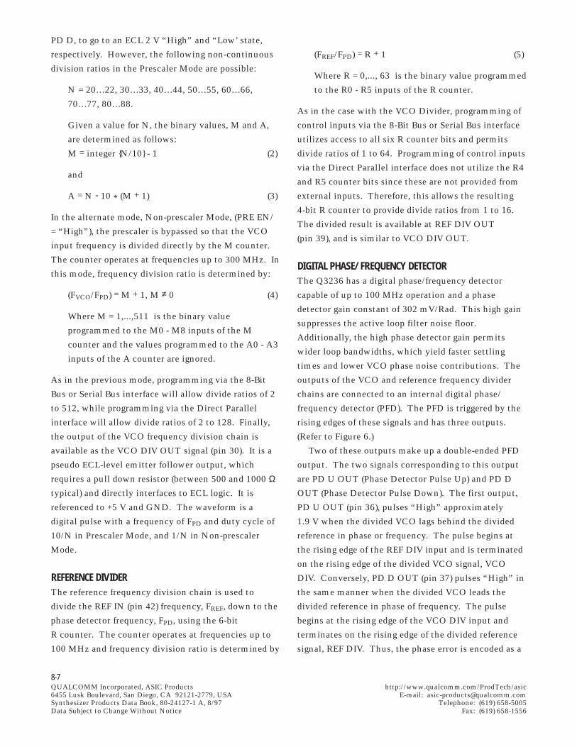
8-7QUALCOMM Incorporated, ASIC Products http://www.qualcomm.com/ProdTech/asic6455 Lusk Boulevard, San Diego, CA 92121-2779, USA E-mail: [email protected] Products Data Book, 80-24127-1 A, 8/97 Telephone: (619) 658-5005Data Subject to Change Without Notice Fax: (619) 658-1556
PD D, to go to an ECL 2 V “High” and “Low’ state,
respectively. However, the following non-continuous
division ratios in the Prescaler Mode are possible:
N = 20…22, 30…33, 40…44, 50…55, 60…66,
70…77, 80…88.
Given a value for N, the binary values, M and A,
are determined as follows:
M = integer N/10 - 1 (2)
and
A = N - 10 * (M + 1) (3)
In the alternate mode, Non-prescaler Mode, (PRE EN/
= “High”), the prescaler is bypassed so that the VCO
input frequency is divided directly by the M counter.
The counter operates at frequencies up to 300 MHz. In
this mode, frequency division ratio is determined by:
(FVCO/FPD) = M + 1, M ≠ 0 (4)
Where M = 1,...,511 is the binary value
programmed to the M0 - M8 inputs of the M
counter and the values programmed to the A0 - A3
inputs of the A counter are ignored.
As in the previous mode, programming via the 8-Bit
Bus or Serial Bus interface will allow divide ratios of 2
to 512, while programming via the Direct Parallel
interface will allow divide ratios of 2 to 128. Finally,
the output of the VCO frequency division chain is
available as the VCO DIV OUT signal (pin 30). It is a
pseudo ECL-level emitter follower output, which
requires a pull down resistor (between 500 and 1000 Ωtypical) and directly interfaces to ECL logic. It is
referenced to +5 V and GND. The waveform is a
digital pulse with a frequency of FPD and duty cycle of
10/N in Prescaler Mode, and 1/N in Non-prescaler
Mode.
REFERENCE DIVIDERThe reference frequency division chain is used to
divide the REF IN (pin 42) frequency, FREF, down to the
phase detector frequency, FPD, using the 6-bit
R counter. The counter operates at frequencies up to
100 MHz and frequency division ratio is determined by
(FREF/FPD) = R + 1 (5)
Where R = 0,..., 63 is the binary value programmed
to the R0 - R5 inputs of the R counter.
As in the case with the VCO Divider, programming of
control inputs via the 8-Bit Bus or Serial Bus interface
utilizes access to all six R counter bits and permits
divide ratios of 1 to 64. Programming of control inputs
via the Direct Parallel interface does not utilize the R4
and R5 counter bits since these are not provided from
external inputs. Therefore, this allows the resulting
4-bit R counter to provide divide ratios from 1 to 16.
The divided result is available at REF DIV OUT
(pin 39), and is similar to VCO DIV OUT.
DIGITAL PHASE/FREQUENCY DETECTORThe Q3236 has a digital phase/frequency detector
capable of up to 100 MHz operation and a phase
detector gain constant of 302 mV/Rad. This high gain
suppresses the active loop filter noise floor.
Additionally, the high phase detector gain permits
wider loop bandwidths, which yield faster settling
times and lower VCO phase noise contributions. The
outputs of the VCO and reference frequency divider
chains are connected to an internal digital phase/
frequency detector (PFD). The PFD is triggered by the
rising edges of these signals and has three outputs.
(Refer to Figure 6.)
Two of these outputs make up a double-ended PFD
output. The two signals corresponding to this output
are PD U OUT (Phase Detector Pulse Up) and PD D
OUT (Phase Detector Pulse Down). The first output,
PD U OUT (pin 36), pulses “High” approximately
1.9 V when the divided VCO lags behind the divided
reference in phase or frequency. The pulse begins at
the rising edge of the REF DIV input and is terminated
on the rising edge of the divided VCO signal, VCO
DIV. Conversely, PD D OUT (pin 37) pulses “High” in
the same manner when the divided VCO leads the
divided reference in phase of frequency. The pulse
begins at the rising edge of the VCO DIV input and
terminates on the rising edge of the divided reference
signal, REF DIV. Thus, the phase error is encoded as a
8-8QUALCOMM Incorporated, ASIC Products http://www.qualcomm.com/ProdTech/asic6455 Lusk Boulevard, San Diego, CA 92121-2779, USA E-mail: [email protected] Products Data Book, 80-24127-1 A, 8/97 Telephone: (619) 658-5005Data Subject to Change Without Notice Fax: (619) 658-1556
pulse-width modulated waveform, whose DC average
is proportional to its duty cycle which equals the phase
error. In typical differential phase detector output
applications, PD U OUT is subtracted from PD D OUT
in a differential OP-AMP active loop integrator filter,
as shown in Figure 13. Therefore, it is only necessary
that the differential output power between the two
phase detector outputs, PU and PD, be linearly
proportionate to the phase difference between the VCO
DIV and REF DIV input rising edges. A residual pulse
width, tRP, is also added onto both phase detector
outputs after the rising edge of the lagging input to
mitigate the usual “dead zone” nonlinearity. This
works as follows: as long as this residual pulse is kept
above a minimum duration, then the phase detector
outputs will always reach full amplitude all the way
down to zero phase difference, thereby maintaining
output power which stays linearly proportionate to the
time skew between the phase detector inputs.
The third output, LD OUT (pin 43), is used for an
out-of-lock indication. It pulses “Low” when either
PD U OUT or PD D OUT is pulsing “High”. Lock
detection is performed by NORing the phase detector
PD U and PD D output signals. The result is a signal
which pulses for a duration equal to the time skew
between the VCO DIV and REF DIV rising edges.
These pulses are integrated with an internal 2K series
resistor, and a shunt capacitor connected to the CEXT
output (pin 34). When the PLL is out of lock and there
is pulsing on the PFD outputs sufficient to bring the
voltage on CEXT above an internal comparator
threshold, then the open collector output, LD OUT,
will turn on, sinking up to 25mA. LD OUT can be
wired to an open-collector fault bus or used to drive an
LED, indicating an out-of-lock condition. The phase/
frequency detector waveforms are shown in Figure 6.
Certain conditions may produce electrical overstress
(EOS) to pin 43 and damage the LD OUT. Such an
occurance would typically be the result of capacitive
discharge with insufficient current limiting resistance
with respect to LD OUT and how out-of-lock
conditions are indicated within a particular system
design. Careful attention to proper current limiting
will eliminate any EOS potential.
DIGITAL PROCESSOR INTERFACE (DPI) MODESThe Q3236 can be programmed using one of three
operating modes including a Direct Parallel Input
Mode, 8-bit Bus Mode, or Serial Bus Mode. All of the
DPI data and control inputs operate at either static or
low speeds relative to the rest of the device and are to
be compatible with CMOS/TTL levels, whose
characteristics are described in Table 6. The DPI
outputs consist of twenty counter programming bits,
M0 - M8, A0 - A3, R0 - R5 as well as the prescaler
enable control input, PRE EN/. An Enhanced
Operation Mode option for the 8-bit Bus and Serial Bus
Modes is provided to enable access to all of these
counter programming bits and is described below. A
Frequency Multiplexing Mode option for the 8-bit Bus
and Serial Bus Modes is also provided to allow rapid
toggling between stored programmed frequencies and
is described below the following sections of these two
respective interface modes.
The interface modes are selected in the following
manner: when the external DPI control signal,
BUSMODE/(pin 22), is “High”, the DPI is in the Direct
Parallel Mode. When the BUSMODE/ input is “Low”,
the DPI is in either the 8-bit Bus or Serial Bus Mode,
depending on the “Low” or “High” state, respectively,
of the SMODE input (pin 21). Serial Mode addressing
is accomplished in a standard fashion using three
signals: SDATA, SCLK, and SEN/. DPI Mode selection
is summarized in Table 1. In order to consolidate the
utility of as many of the package pins as possible, most
of the CMOS/TTL inputs are multi-functional as
denoted in Figure 10. This is possible because some of
the DPI Modes and the inputs are mutually exclusive.
Internally, these differing control signal inputs are
logically OR’ed to avoid contention.
Table 1. Digital Processor Interface (DPI) Mode Selection
BUSMODE/INPUT
LOWLOWHIGH
SMODEINPUT
LOWHIGH
X
DPI MODE
8-BIT BUSSERIAL BUS
DIRECT PARALLEL INPUT
8-9QUALCOMM Incorporated, ASIC Products http://www.qualcomm.com/ProdTech/asic6455 Lusk Boulevard, San Diego, CA 92121-2779, USA E-mail: [email protected] Products Data Book, 80-24127-1 A, 8/97 Telephone: (619) 658-5005Data Subject to Change Without Notice Fax: (619) 658-1556
ENHANCED OPERATION or Q3036 MODEAn enhanced operation mode control signal, Q3036
MODE/(pin 44), is referenced after QUALCOMM’s
original single-chip PLL, the Q3036. It allows the
Q3236 to maintain identical DPI Modes and divider
ratios as the Q3036 for backwards compatibility, or
be set for expanded divider capability and DPI
operation. When the Q3036 MODE/ input is “High”,
this enables access to all twenty counter programming
bits for operation only in the 8-bit Bus or Serial Bus
Modes if the additional M7, M8 or R4, R5 counter bits
are required for larger division ratios. This allows for
programmability to the full range of divider ratios as
described in the Functional Overview section under
the VCO Divider and Reference Divider subsections.
When the Q3036 MODE/ input is “Low”, all of the
counter programming bits except M7, M8, R4, and R5
are available in all three interface modes, with a
corresponding reduction in the available range of
divider ratios as mentioned in the previous section.
When operating with Q3036 MODE/ set “Low”, the
M7, M8, R4, and R5 inputs are set internally to the
“Low” state. This allows any previously designed
synthesizer circuits using the Q3036 to be directly
replaced with the Q3236 device.
Additionally, all external CMOS/TTL inputs will
register as a “High” or “Low” state when left floating,
according to the “Low” or “High” state of the Q3036
MODE/ input, respectively. This however, means
that when operating in 8-bit Bus Mode or Serial Bus
Mode when pin 44 is tied “Low”, the FSELP and
FSELS inputs (pins 18 and 16, respectively) must also
be tied “Low” so that the data loaded into the primary
registers can remain inactive until after the HOP WR
input is asserted. (See section under 8-bit Bus or
Serial Bus Frequency Multiplexing: Ping-Pong Mode
for further details.)
DIRECT PARALLEL INPUT MODEWith the BUSMODE/ input set “High” and the Q3036
MODE/ input set “Low”, all of the DPI outputs
except M7, M8, R4, and R5 are taken directly from
external inputs, as listed in the pin assignment/
descriptions in Table 8J. Referring to the Q3236 Block
Diagram (Figure 1), BUSMODE/ is really the select
input to a row of 20 x 2:1 MUXes. Each of the inputs
are connected to the external inputs, with the
exception of the M7, M8, R4, and R5 signals. This
mode allows the device to be hardwired for fixed
frequency phase-locked oscillators as well as parallel-
loaded fast frequency hopping applications.
8-BIT BUS MODEWith the BUSMODE/ input “Low” and the SMODE
input “Low”, the 8-bit Bus Mode is selected and the
external DBUS0-7 inputs are latched into one of the
three primary registers, with the A WR, M1 WR, or
M2 WR external control inputs according to the
timing requirements shown in Figure 8. In the 8-bit
Bus Mode, the interface is double-buffered consisting
of a set of primary registers and secondary registers.
The primary registers are programmed in parallel
fashion without affecting the inputs to the counters.
The contents from the primary registers are loaded
into the secondary registers on the rising edge of the
HOP WR input and are then immediately available to
the counters and prescaler as DPI outputs. The DPI
outputs are simply the secondary register outputs. A
mapping of the DBUS0-7 inputs to the primary
registers for all twenty counter programming bits is
shown in Table 2, and listed in the pin assignment/
descriptions in Table 8H. Note however, that when
operating in the 8-bit Bus Mode and the Q3036 Mode
(pin 44 tied “Low”), it is necessary to also tie “Low”
the R2 and R3 external reference counter inputs (pins
4 and 5, respectively) in order for the 8-bit bus to
program correctly. This requirement is due to the
DBUS0-1 inputs sharing the R2-3 input pads which
automatically register to the opposite logic state of
pin 44 when left floating. A failure to set pins 4 and 5
“Low” when operating this way will result in the
internal M0-1 and A0-1 programming counter bits
being stuck in a logic “High” condition.
SERIAL BUS MODEWith the BUSMODE/ input “Low” and the SMODE
input “High”, the Serial Bus Mode is selected and
data is shifted serially into the SDATA input on the
8-10QUALCOMM Incorporated, ASIC Products http://www.qualcomm.com/ProdTech/asic6455 Lusk Boulevard, San Diego, CA 92121-2779, USA E-mail: [email protected] Products Data Book, 80-24127-1 A, 8/97 Telephone: (619) 658-5005Data Subject to Change Without Notice Fax: (619) 658-1556
rising edge of the SCLK input, while the active “Low”
shift enable control input, SEN/, is “Low”. In the
same manner as the 8-bit Bus Mode, the interface is
double-buffered consisting of a set of primary registers
and secondary registers. The data for all twenty
counter programming bits is shifted into the primary
registers in accordance to the sequence shown in
Table 3, starting with R5 and ending with A0. When
operating in the Q3036 Mode (pin 44 tied “Low”), all
twenty serial data bits still need to be shifted into the
SDATA input even though the M7-8 and R4-5 counter
bits cannot be utilized. In this case, a logic “0”
should be used for the first four data bits of the
SDATA input. The contents from the primary
registers are shifted into the secondary registers on the
rising edge of either the SEN/ input or the HOP WR
input asserted according to the timing requirements
shown in Figure 9, and are then immediately available
to the counters and prescaler as DPI outputs. A list of
the respective Serial Bus Mode pin assignment/
descriptions is shown in Table 8I.
8-BIT BUS OR SERIAL BUS FREQUENCY MULTIPLEXING:PING-PONG MODEThe Ping-Pong Mode is a subset of both the 8-bit Bus
and Serial Bus Modes which enables the Q3236 to be
multiplexed between two pre-loaded frequencies for
applications involving random frequency hopping, low-
data-rate FSK modulation, or half-duplex transceiving
operation using a single synthesizer. ATE system
environments requiring multiple frequencies also use
fast switching synthesizers to greatly increase system
throughput, and they are increasingly being used as the
reference oscillator in commercial Magnetic
Resonance Imaging (MRI) systems. In either interface
mode, this is carried out by toggling between two
different VCO division ratios in the primary and
secondary registers, since the counter programming
bits in the primary registers may be updated while the
ones in the secondary registers are controlling the
programmable divider.
The so-called “ping-pong” frequency selection is
controlled by the external input signal, FSELP in the
8-bit Bus Mode, and FSELS in the Serial Mode.
As noted in the 8-bit Bus Mode subsection, after the
DBUS0-7 inputs are latched into the three primary
registers, they are then only loaded into the secondary
registers after the HOP WR input is asserted. This
means that the contents of the primary registers can be
updated with a new frequency word while the
Table 2. 8-bit Bus Mode Primary Register Map
INTERNAL PRIMARY REGISTER MAPPINGM1 WR
RISING EDGE
M0M1M2M3M4M5M6
PRE EN/
A WRRISING EDGE
A0A1A2A3R0R1R2R3
M2 WRRISING EDGE
M7M8R4R5
N/AN/AN/AN/A
EXTERNALINPUT
DBUS0DBUS1DBUS2DBUS3DBUS4DBUS5DBUS6DBUS7
BIT NO.
SDATAINPUT
1
R5
2
R4
3
M8
4
M7
5
PREEN/
6
M6
7
M5
8
M4
9
M3
10
M2
11
M1
12
M0
13
R3
14
R2
15
R1
16
R0
17
A3
18
A2
19
A1
20
A0
Table 3. Serial Mode Data Programming Sequence
8-11QUALCOMM Incorporated, ASIC Products http://www.qualcomm.com/ProdTech/asic6455 Lusk Boulevard, San Diego, CA 92121-2779, USA E-mail: [email protected] Products Data Book, 80-24127-1 A, 8/97 Telephone: (619) 658-5005Data Subject to Change Without Notice Fax: (619) 658-1556
secondary registers retain control of the DPI outputs
with the previously loaded data. An external
frequency multiplexing control input, FSELP (pin 18),
enables the device to be toggled between these two
pre-loaded frequencies as noted in the pin assignment/
descriptions, Table 8H. When the FSELP input is
“High”, the synthesizer output frequency is obtained
from the frequency word stored in the primary
registers, and when the FSELP input is “Low”, the
output frequency is obtained from the frequency word
stored in the secondary registers. The DPI outputs are
simply the multiplexed output of either the primary or
secondary register outputs selected by the control
signal FSELP.
As noted in the Serial Bus Mode subsection, after
the data for all twenty counter programming bits is
shifted into the primary registers, they are then only
loaded into the secondary registers after the SEN/ and
HOP WR inputs are asserted. In the same manner as
in the 8-bit Bus Mode, an external frequency
multiplexing control input, FSELS (pin 16), enables the
device to be toggled between these two pre-loaded
frequencies as noted in the pin assignment/
descriptions in Table 8I. The synthesizer output
frequency is simply the multiplexed output of either
the primary or secondary register outputs selected by
the “High” or “Low” state, respectively, of the control
signal FSELS.
For Q3236 implementation using the Ping-Pong
Mode for FSK modulation of the synthesizer’s output,
the data rate limitation of the loop will be a function
of the natural frequency, ωn, since a second-order PLL
is able to track for phase and frequency modulations of
the reference signal as long as the modulation
frequencies remain within an angular frequency band
roughly between zero and ωn. When using the Ping-
Pong Mode for a frequency hopping synthesizer, or as a
transmit and receive synthesizer for half-duplex
operation, the synthesizer’s switching speed
performance, otherwise known as it’s settling time
characteristics, will essentially govern the achievable
switching or hop rate, although the 20-bit load period
for the respective interface mode used should also be
taken into account.
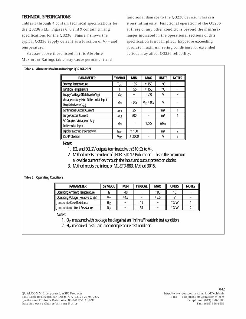
8-12QUALCOMM Incorporated, ASIC Products http://www.qualcomm.com/ProdTech/asic6455 Lusk Boulevard, San Diego, CA 92121-2779, USA E-mail: [email protected] Products Data Book, 80-24127-1 A, 8/97 Telephone: (619) 658-5005Data Subject to Change Without Notice Fax: (619) 658-1556
functional damage to the Q3236 device. This is a
stress rating only. Functional operation of the Q3236
at these or any other conditions beyond the min/max
ranges indicated in the operational sections of this
specification is not implied. Exposure exceeding
absolute maximum rating conditions for extended
periods may affect Q3236 reliability.
TECHNICAL SPECIFICATIONSTables 1 through 4 contain technical specifications for
the Q3236 PLL. Figures 6, 8 and 9 contain timing
specifications for the Q3236. Figure 7 shows the
typical Q3236 supply current as a function of VCC and
temperature.
Stresses above those listed in this Absolute
Maximum Ratings table may cause permanent and
Table 4. Absolute Maximum Ratings: Q3236I-20N
PARAMETER
Storage TemperatureJunction TemperatureSupply Voltage (Relative to VEE)Voltage on Any Non Differential Input Pin (Relative to VEE)Continuous Output CurrentSurge Output CurrentAC Coupled Voltage on Any Differential InputBipolar Latchup InsensitivityESD Protection
Notes: 1. ECL and ECL 2V outputs terminated with 510 Ω to VEE. 2. Method meets the intent of JEDEC STD 17 Publication. This is the maximum allowable current flow through the input and output protection diodes. 3. Method meets the intent of MIL-STD-883, Method 3015.
SYMBOL
TSTO
TJ
VCC
VIN
IOUT
IOUT
VIN
ITRIG
VESD
MIN - 55- 55–
- 0.5
25200
–
± 100± 2000
MAX+ 150+ 150+ 7.0
VCC + 0.5
––
1275
––
UNITS
°C°CV
V
mAmA
mVPP
mAV
NOTES–––
–
11
–
23
Table 5. Operating Conditions
PARAMETER
Operating Ambient TemperatureOperating Voltage (Relative to VEE)Junction to Case ResistanceJunction to Ambient Resistance
Notes: 1. θJC measured with package held against an "infinite" heatsink test condition. 2. θJA measured in still-air, room temperature test condition.
SYMBOL
TA
VCC
θJC
θJA
MIN-40
+4.5––
TYPICAL––1951
MAX+85+5.5
––
UNITS
°CV
°C/W°C/W
NOTES––12
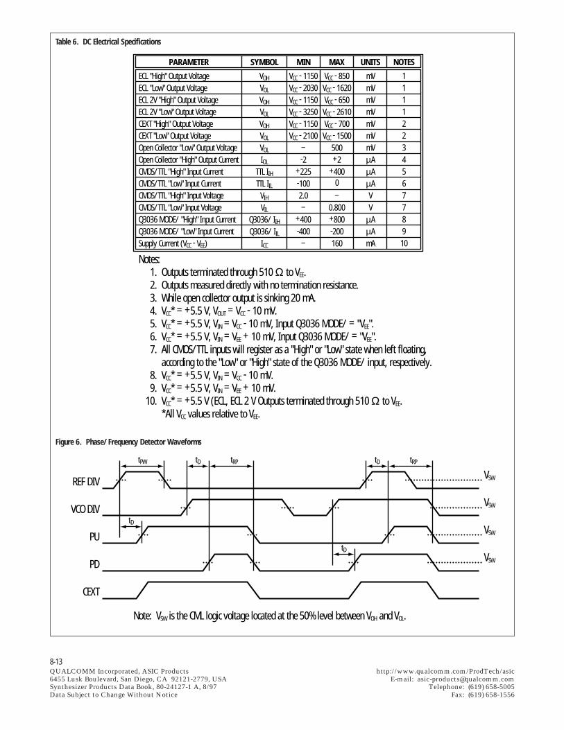
8-13QUALCOMM Incorporated, ASIC Products http://www.qualcomm.com/ProdTech/asic6455 Lusk Boulevard, San Diego, CA 92121-2779, USA E-mail: [email protected] Products Data Book, 80-24127-1 A, 8/97 Telephone: (619) 658-5005Data Subject to Change Without Notice Fax: (619) 658-1556
Table 6. DC Electrical Specifications
PARAMETER
ECL "High" Output VoltageECL "Low" Output VoltageECL 2V "High" Output VoltageECL 2V "Low" Output VoltageCEXT "High" Output VoltageCEXT "Low" Output VoltageOpen Collector "Low" Output VoltageOpen Collector "High" Output CurrentCMOS/TTL "High" Input CurrentCMOS/TTL "Low" Input CurrentCMOS/TTL "High" Input VoltageCMOS/TTL "Low" Input VoltageQ3036 MODE/ "High" Input CurrentQ3036 MODE/ "Low" Input CurrentSupply Current (VCC - VEE)
Notes: 1. Outputs terminated through 510 Ω to VEE. 2. Outputs measured directly with no termination resistance. 3. While open collector output is sinking 20 mA. 4. VCC* = +5.5 V, VOUT = VCC - 10 mV. 5. VCC* = +5.5 V, VIN = VCC - 10 mV, Input Q3036 MODE/ = "VEE". 6. VCC* = +5.5 V, VIN = VEE + 10 mV, Input Q3036 MODE/ = "VEE". 7. All CMOS/TTL inputs will register as a "High" or "Low" state when left floating, according to the "Low" or "High" state of the Q3036 MODE/ input, respectively. 8. VCC* = +5.5 V, VIN = VCC - 10 mV. 9. VCC* = +5.5 V, VIN = VEE + 10 mV. 10. VCC* = +5.5 V (ECL, ECL 2 V Outputs terminated through 510 Ω to VEE. *All VCC values relative to VEE.
SYMBOL
VOH
VOL
VOH
VOL
VOH
VOL
VOL
IOL
TTL IIHTTL IIL
VIH
VIL
Q3036/ IIHQ3036/ IIL
ICC
MIN
VCC - 1150VCC - 2030VCC - 1150VCC - 3250VCC - 1150VCC - 2100
–-2
+225-1002.0–
+400-400
–
MAX
VCC - 850VCC - 1620VCC - 650
VCC - 2610VCC - 700
VCC - 1500500+2
+4000–
0.800+800-200160
UNITS
mVmVmVmVmVmVmVµAµAµAVV
µAµAmA
NOTES
11112234567789
10
tPW tD tRP
tD
tD
tD tRP
REF DIV
VCO DIV
PU
PD
CEXT
Note: VSW is the CML logic voltage located at the 50% level between VOH and VOL.
VSW
VSW
VSW
VSW
Figure 6. Phase/Frequency Detector Waveforms
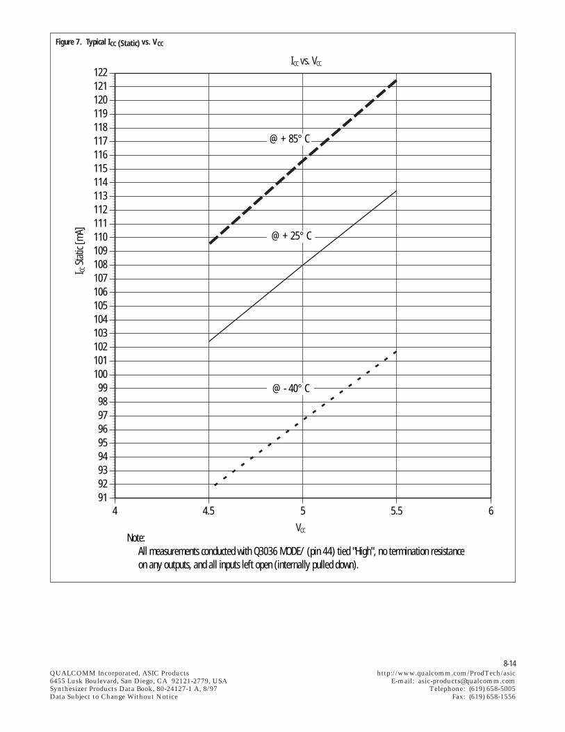
8-14QUALCOMM Incorporated, ASIC Products http://www.qualcomm.com/ProdTech/asic6455 Lusk Boulevard, San Diego, CA 92121-2779, USA E-mail: [email protected] Products Data Book, 80-24127-1 A, 8/97 Telephone: (619) 658-5005Data Subject to Change Without Notice Fax: (619) 658-1556
919293949596979899
100101102103104105106107108109110111112113114115116117118119120121122
4 4.5 5 5.5 6
@ - 40° C
@ + 25° C
@ + 85° C
VCC
I CC St
atic
[mA]
Note: All measurements conducted with Q3036 MODE/ (pin 44) tied "High", no termination resistance on any outputs, and all inputs left open (internally pulled down).
ICC vs. VCC
Figure 7. Typical ICC (Static) vs. VCC
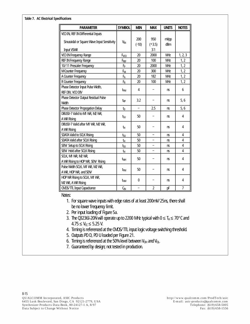
8-15QUALCOMM Incorporated, ASIC Products http://www.qualcomm.com/ProdTech/asic6455 Lusk Boulevard, San Diego, CA 92121-2779, USA E-mail: [email protected] Products Data Book, 80-24127-1 A, 8/97 Telephone: (619) 658-5005Data Subject to Change Without Notice Fax: (619) 658-1556
Table 7. AC Electrical Specifications
PARAMETER
VCO IN, REF IN Differential Inputs
Sinusoidal or Square Wave Input Sensitivity
Input VSWRVCO IN Frequency RangeREF IN Frequency Range10/11 Prescaler FrequencyM Counter FrequencyA Counter FrequencyR Counter FrequencyPhase Detector Input Pulse Width,REF DIV, VCO DIVPhase Detector Output Residual PulseWidthPhase Detector Propogation DelayDBUS0-7 Valid to M1 WR, M2 WR,A WR RisingDBUS0-7 Valid after M1 WR, M2 WR,A WR RisingSDATA Valid to SCLK RisingSDATA Valid after SCLK RisingSEN/ Setup to SCLK RisingSEN/ Hold after SCLK RisingSCLK, M1 WR, M2 WR, A WR Rising to HOP WR, SEN/ RisingPulse Width SCLK, M1 WR, M2 WR,A WR, HOP WR, and SEN/HOP WR Rising to SCLK, M1 WR, M2 WR, A WR RisingCMOS/TTL Input Capacitance
Notes: 1. For square wave inputs with edge rates of at least 200mV/25ns, there shall be no lower frequency limit. 2. Per input loading of Figure 5a. 3. The Q3236I-20N will operate up to 2200 MHz typical with 0 ≤ TA ≤ 70°C and 4.75 ≤ VCC ≤ 5.25 V. 4. Timing is referenced at the CMOS/TTL input logic voltage switching threshold. 5. Outputs PD D, PD U loaded per Figure 21. 6. Timing is referenced at the 50% level between VOH and VOL. 7. Guaranteed by design; not tested in production.
SYMBOL
VIN
FVCO
FREF
FP
FM
FA
FR
tPW
tRP
tD
tSU
tH
tSU
tHtSU
tH
tWH
tPW
tHW
CIN
MIN
200(-10)
202020202020
4
3.2
–
50
50
50505050
50
50
0
–
MAX
950(+3.5)
3:12000100
2000300182100
–
–
2.5
–
–
––––
–
–
–
2
UNITS
mVppdBm
MHzMHzMHzMHzMHzMHz
ns
ns
ns
ns
ns
nsnsnsns
ns
ns
ns
pF
NOTES
1, 2, 31, 21, 21, 21, 21, 2
6
5, 6
5, 6
4
4
4444
4
4
4
7
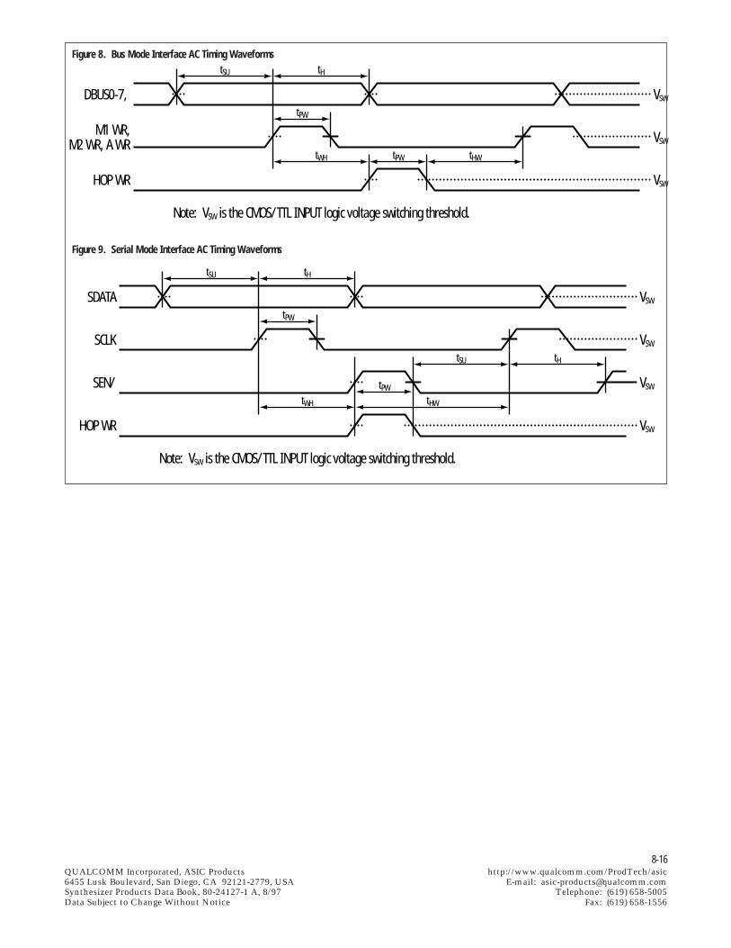
8-16QUALCOMM Incorporated, ASIC Products http://www.qualcomm.com/ProdTech/asic6455 Lusk Boulevard, San Diego, CA 92121-2779, USA E-mail: [email protected] Products Data Book, 80-24127-1 A, 8/97 Telephone: (619) 658-5005Data Subject to Change Without Notice Fax: (619) 658-1556
Figure 8. Bus Mode Interface AC Timing Waveforms
Note: VSW is the CMOS/TTL INPUT logic voltage switching threshold.
VSW
VSW
VSW
DBUS0-7,
M1 WR, M2 WR, A WR
HOP WR
tSU tH
tPW
tPWtWH tHW
Note: VSW is the CMOS/TTL INPUT logic voltage switching threshold.
VSW
VSW
VSW
VSW
SDATA
SCLK
SEN/
HOP WR
tSU tH
tPW
tPW
tWH
tSU tH
tHW
Figure 9. Serial Mode Interface AC Timing Waveforms
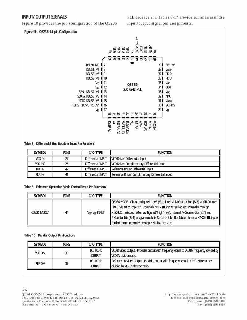
8-17QUALCOMM Incorporated, ASIC Products http://www.qualcomm.com/ProdTech/asic6455 Lusk Boulevard, San Diego, CA 92121-2779, USA E-mail: [email protected] Products Data Book, 80-24127-1 A, 8/97 Telephone: (619) 658-5005Data Subject to Change Without Notice Fax: (619) 658-1556
SYMBOL
VCO INVCO IN/REF INREF IN/
PINS
27284241
I/O TYPE
Differential INPUTDifferential INPUTDifferential INPUTDifferential INPUT
FUNCTION
VCO Driven Differential InputVCO Driven Complimentary Differential InputReference Driven Differential InputReference Driven Complimentary Differential Input
Table 8. Differential Line Receiver Input Pin Functions
Table 10. Divider Output Pin Functions
SYMBOL
VCO DIV
REF DIV
PINS
30
39
I/O TYPE
ECL 100 kOUTPUT
ECL 100 kOUTPUT
FUNCTION
VCO Divided Output. Provides output with frequency equal to VCO IN frequency divided byVCO IN division ratio.Reference Divided Output. Provides output with frequency equal to REF IN frequencydivided by REF IN division ratio.
Table 9. Enhanced Operation Mode Control Input Pin Functions
SYMBOL
Q3236 MODE/
PINS
44
I/O TYPE
VCC/VEE INPUT
FUNCTION
Q3036 MODE. When configured "Low" (VEE), internal M-Counter Bits [8:7] and R-CounterBits [5:4] set to logic "0". External CMOS/TTL inputs "pulled up" internally through> 50 kΩ resistors. When configured "High" (VCC), internal M-Counter Bits [8:7] andR-Counter bits [5:4] programmable in Serial or 8-bit Bus Mode. External CMOS/TTL inputs"pulled down" internally through > 50 kΩ resistors.
INPUT/OUTPUT SIGNALSFigure 10 provides the pin configuration of the Q3236
Figure 10. Q3236 44-pin Configuration
DBUS0, MODBUS1, M1DBUS2, M2DBUS3, M3
VCCVCC
SEN/, DBUS4, M4SDATA, DBUS5, M5
SCLK, DBUS6, M6FSELS, DBUS7, PRE EN/
VEE
REF DIVVCCO2PD DPD UVCCCEXTVCCN/CVCCO1VCO DIVVEE
V EE
R3 IN
R2 IN
R1 IN
R0 IN
V CC
Q303
6 MO
DE/
LD O
UTRE
F IN
REF I
N/V E
E
VCO IN/VCO INHOP WRA WRM1 WRVCCBUS MODE/SMODE, A3M2 WR, A2A1FSELP, A0
7891011121314151617
6 5 4 3 2 1 44 43 42 41 40
39383736353433323130292827262524232221201918
Q32362.0 GHz PLL
PLL package and Tables 8-17 provide summaries of the
input/output signal pin assignments.
8-18QUALCOMM Incorporated, ASIC Products http://www.qualcomm.com/ProdTech/asic6455 Lusk Boulevard, San Diego, CA 92121-2779, USA E-mail: [email protected] Products Data Book, 80-24127-1 A, 8/97 Telephone: (619) 658-5005Data Subject to Change Without Notice Fax: (619) 658-1556
Table 11. Phase Detector Output Pin Functions
Table 12. Phase Lock Detect Output Pin Functions
Table 13. Unconnected Pin Functions
Table 14. Voltage Supply Pin Functions
SYMBOL
PD U
PD D
PINS
36
37
I/O TYPE
ECL 2 V 100 kOUTPUT
ECL 2 V 100 kOUTPUT
FUNCTION
Phase Detect Pulse "Up". Pulses "High" when VCO DIV lags REF DIV.
Phase Detect Pulse "Down". Pulsed "High" when VCO DIV leads REF DIV.
SYMBOL
LD OUT
CEXT
PINS
43
34
I/O TYPE
TTL Open Collector
Series 2 k ECL OUTPUT
FUNCTION
Lock Detect. High impedance during phase-locked operation, low impedance during phaseunlocked operation.C EXTERNAL. OR'd output of PD and PU provided by 100 k ECL emitter followerterminated through 2 k, on chip, series resistance. External attachment of 0.1 µFcapacitor acts to low pass filter OR'd output of PD and PU signals. Output drives invertingdifferential input of on-chip comparator used for switching LD OUT.
SYMBOL–
PINS
32
I/O TYPE
N/C
FUNCTION
Unconnected Pin
SYMBOL
VCC
VCCO1
VCCO2
VEE
PINS
1, 11, 12, 23, 33, 353138
6, 17, 29, 40
I/O TYPE
PowerPowerPowerPower
FUNCTION
Core Circuitry VCC POWER SUPPLYOutput Drivers VCC POWER SUPPLY for VCO DIV OUT and CEXTOutput Drivers VCC POWER SUPPLY for PD U OUT, PD D OUT and REF DIV OUTVEE POWER SUPPLY
Table 15. Digital Processor Interface (DPI) 8-bit Bus Mode Pin Functions
SYMBOL
BUSMODE/
SMODE
DBUS7-DBUS0
M1 WR
M2 WR
A WR
HOP WR
FSELP
PINS
22
21
16 (MSB), 15, 14, 13,10, 9, 8, 7 (LSB)
24
20
25
26
18
I/O TYPE
CMOS/TTL INPUT
CMOS/TTL INPUT
CMOS/TTL INPUT
CMOS/TTL INPUT
CMOS/TTL INPUT
CMOS/TTL INPUT
CMOS/TTL INPUT
CMOS/TTL INPUT
FUNCTION
BUSMODE. Used with SMODE to select one of three possible DPI modes of operation.SMODE. Selects SERIAL BUS MODE (BUSMODE/ "Low", SMODE "High") or 8-bit BUS MODE(BUSMODE/ "Low", SMODE "Low")
DATA BUS bit 7 (MSB) - DATA bus bit 0 (LSB)
M1 WRITE. Rising edge active. Latches DATA BUS bits [7:0] (PRE EN/ and M[6:0])to primary register.M2 WRITE. Rising edge active. Latches DATA BUS bits [3:0] (R[5:4] and M[8:7]) to primary register.A WRITE. Rising edge active. Latches DATA BUS bits [7:0] (R[3:0] and A[3:0]) to primary register.HOP WRITE. Rising edge active. Latches primary register data previously latched withM1 WR, M2 WR, and A WR, to secondary register.Provides option of selecting DPI information stored in primary registers (FSLEP = "1") orsecondary registers (FSELP = "0").
8-19QUALCOMM Incorporated, ASIC Products http://www.qualcomm.com/ProdTech/asic6455 Lusk Boulevard, San Diego, CA 92121-2779, USA E-mail: [email protected] Products Data Book, 80-24127-1 A, 8/97 Telephone: (619) 658-5005Data Subject to Change Without Notice Fax: (619) 658-1556
Table 16. Digital Processor Interface (DPI) Serial Bus Mode Pin Functions
SYMBOL
SDATA
SEN/
SCLK
HOP WR
FSELS
PINS
14
13
15
26
16
I/O TYPE
CMOS/TTL INPUT
CMOS/TTL INPUT
CMOS/TTL INPUT
CMOS/TTL INPUT
CMOS/TTL INPUT
FUNCTION
SERIAL DATA. Data is shifted serially into input SDATA on rising edge of SCLK signal.SHIFT ENABLE. Active "Low" for SERIAL DATA loading with input SDATA. Also latchesprimary registers SERIAL DATA into secondary registers. SEN/ or HOP WR must beasserted "High" when loading SERIAL DATA to secondary registers.SHIFT CLOCK. Rising edge active. Shifts serial data into input SDATA with each rising edge(SEN/ = "Low").HOP WRITE. Rising edge active. Latches primary registers SERIAL DATA into secondaryregisters. SEN/ or HOP WR must be asserted "High" when loading SERIAL DATA tosecondary registers.Provides option of selecting DPI information stored in primary registers (FSELS = "1") orsecondary registers (FSELS = "0").
Table 17. Digital Processor Interface (DPI) Direct Parallel Input Mode Pin Functions
SYMBOL
M[6:0]
A[3:0]
R[3:0]PRE EN/
PINS
15 (MSB), 14, 13, 10,9, 8, 7 (LSB)
21 (MSB), 20, 19,18 (LSB)
5 (MSB), 4, 3, 2 (LSB)16
I/O TYPE
CMOS/TTL INPUT
CMOS/TTL INPUT
CMOS/TTL INPUTCMOS/TTL INPUT
FUNCTION
M-COUNTER BITS 6 (MSB) - 0 (LSB)
A-COUNTER BITS 3 (MSB) - 0 (LSB)
R-COUNTER BITS 3 (MSB) - 0 (LSB)PRESCALER ENABLE. Enables Divide-by 10/11 Prescaler (Active "Low")
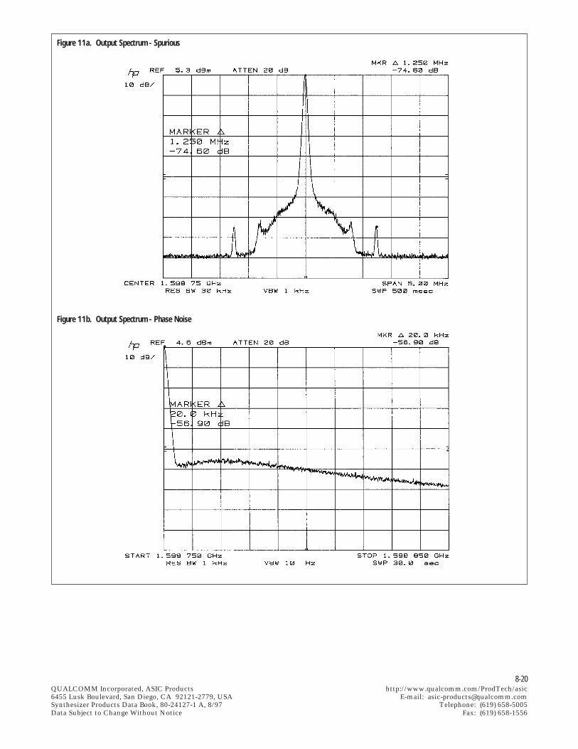
8-20QUALCOMM Incorporated, ASIC Products http://www.qualcomm.com/ProdTech/asic6455 Lusk Boulevard, San Diego, CA 92121-2779, USA E-mail: [email protected] Products Data Book, 80-24127-1 A, 8/97 Telephone: (619) 658-5005Data Subject to Change Without Notice Fax: (619) 658-1556
Figure 11a. Output Spectrum - Spurious
Figure 11b. Output Spectrum - Phase Noise
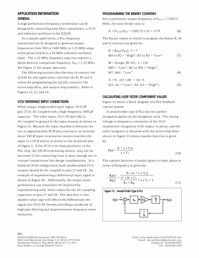
8-21QUALCOMM Incorporated, ASIC Products http://www.qualcomm.com/ProdTech/asic6455 Lusk Boulevard, San Diego, CA 92121-2779, USA E-mail: [email protected] Products Data Book, 80-24127-1 A, 8/97 Telephone: (619) 658-5005Data Subject to Change Without Notice Fax: (619) 658-1556
PROGRAMMING THE BINARY COUNTERSFor a synthesizer output frequency of FVCO = 1598.75
MHz, the total divide ratio is:
N = FVCO/FPD = 1598.75/1.25 = 1279 (6)
The binary values in which to program the binary R, M
and A counters are given by:
R = (FREF/FPD) - 1 = 7
(R0 to R2 = “High”; R3 to R5 = “Low” (7)
M = Integer N/10 - 1 = 126
(M0 = “Low”; M1 to M6 = “High”;
M7, M8 = “Low” (8)
A = N - (10 * (M + 1)) = 9
(A1, A2 = “Low”; A0, A3 = “High”) (9)
CALCULATING LOOP FILTER COMPONENT VALUESFigure 12 shows a block diagram of a PLL feedback
control system.
A second order type II PLL has two perfect
integrators (poles on the imaginary axis). The tuning
voltage-to-frequency conversion of the VCO
implements integration with respect to phase, and the
other integrator is obtained with the active loop filter
shown in Figure 13 whose transfer function is given
by:
(10)
The transfer function of output phase to input phase in
terms of frequency is given by:
(11)
APPLICATION INFORMATIONGENERALA high performance frequency synthesizer can be
designed by connecting loop filter components, a VCO
and reference oscillator to the Q3236.
As a sample application, a PLL frequency
synthesizer can be designed to generate output
frequencies from 900 to 1600 MHz in 1.25 MHz steps
while phase locked to a 10 MHz reference oscillator
input. The 1.25 MHz frequency step size requires a
phase detector comparison frequency, FPD = 1.25 MHz.
See Figure 11 for output spectrum.
The following sections describe how to connect the
Q3236 for this application, calculate the R, M and A
values for programming the Q3236, construct the
active loop filter, and analyze loop stability. Refer to
Figures 12, 13, and 14.
VCO/REFERENCE INPUT CONNECTIONSWhen using a single-ended input signal, VCO IN
(pin 27) is AC-coupled with a high frequency 1000 pF
capacitor. The other input, VCO IN/(pin 28), is
AC-coupled to ground in the same manner as shown in
Figure 5a. Because the input impedance between the
two is approximately 80 Ω plus reactance, an external
shunt 100 Ω input termination resistor matches the
input to a 50 Ω source as shown in the measured plot
of Figure 3. If the VCO is in close proximity to the
PLL chip, the 100 Ω terminating resistor may not be
necessary if the connecting trace is short enough not to
warrant transmission line design considerations. In a
balanced 50 Ω configuration, both double-ended VCO
outputs should be AC-coupled to pins 27 and 28. An
example of implementing a differential input signal is
shown in Figure 5b. Additionally, the output noise
performance can sometimes be improved by
experimenting with lower values for the AC-coupling
capacitors to pins 27 and 28. The idea here is that
smaller-value caps will effectively differentiate the
signal into VCO IN thereby providing a modicum of
high pass filtering and improved lower frequency noise
immunity.
Figure 12. Second Order Type II PLL
θi(s)+
Σ θo(s)Kφ F(s) KVs
1N
–
F(s) = (1 + s * T2)
s * T1
θo(s)
θi(s)=
N * (1 + s * T2)
s2 * N * T1
KV * Kφ + s * T2 + 1
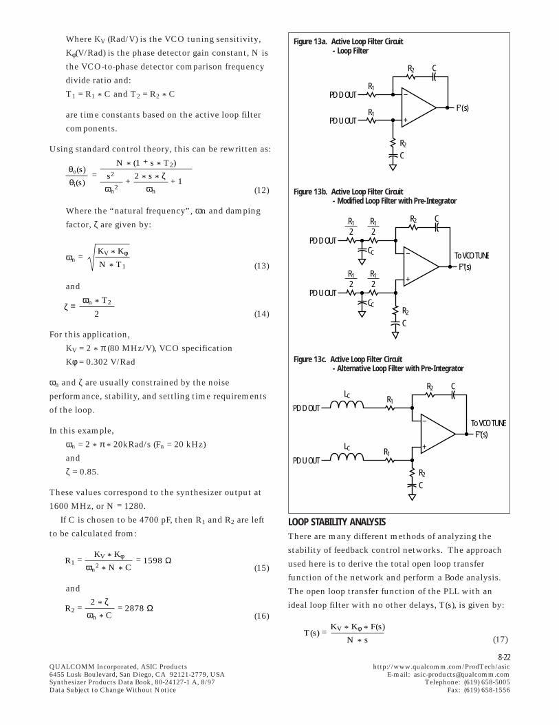
8-22QUALCOMM Incorporated, ASIC Products http://www.qualcomm.com/ProdTech/asic6455 Lusk Boulevard, San Diego, CA 92121-2779, USA E-mail: [email protected] Products Data Book, 80-24127-1 A, 8/97 Telephone: (619) 658-5005Data Subject to Change Without Notice Fax: (619) 658-1556
Where KV (Rad/V) is the VCO tuning sensitivity,
Kφ(V/Rad) is the phase detector gain constant, N is
the VCO-to-phase detector comparison frequency
divide ratio and:
T1 = R1 * C and T2 = R2 * C
are time constants based on the active loop filter
components.
Using standard control theory, this can be rewritten as:
(12)
Where the “natural frequency”, ωn and damping
factor, ζ are given by:
(13)
and
(14)
For this application,
KV = 2 * π (80 MHz/V), VCO specification
Kφ = 0.302 V/Rad
ωn and ζ are usually constrained by the noise
performance, stability, and settling time requirements
of the loop.
In this example,
ωn = 2 * π * 20kRad/s (Fn = 20 kHz)
and
ζ = 0.85.
These values correspond to the synthesizer output at
1600 MHz, or N = 1280.
If C is chosen to be 4700 pF, then R1 and R2 are left
to be calculated from:
(15)
and
(16)
Figure 13a. Active Loop Filter Circuit - Loop Filter
ωn = KV * Kφ
N * T1
θo(s)
θi(s)=
N * (1 + s * T2)
s2
ωn2
+ 2 * s * ζ
ωn + 1
ωn * T2
2ζ =
R1 = = 1598 Ω KV * Kφ
ωn2 * N * C
R2 = = 2878 Ω 2 * ζ
ωn * C
PD D OUT
PD U OUT
R1
R1
R2
R2
C
–
+
C
F'(s)
Figure 13b. Active Loop Filter Circuit - Modified Loop Filter with Pre-Integrator
PD D OUT
PD U OUT
R2R12
CC
R2
C
–
+
C
F"(s)
R12
R12
CC
R12
To VCO TUNE
Figure 13c. Active Loop Filter Circuit - Alternative Loop Filter with Pre-Integrator
PD D OUT
PD U OUT
R2
R1
R2
C
–
+
C
F"(s)
LC
LC R1
To VCO TUNE
LOOP STABILITY ANALYSISThere are many different methods of analyzing the
stability of feedback control networks. The approach
used here is to derive the total open loop transfer
function of the network and perform a Bode analysis.
The open loop transfer function of the PLL with an
ideal loop filter with no other delays, T(s), is given by:
(17)T(s) =
KV * Kφ * F(s)
N * s
8-23QUALCOMM Incorporated, ASIC Products http://www.qualcomm.com/ProdTech/asic6455 Lusk Boulevard, San Diego, CA 92121-2779, USA E-mail: [email protected] Products Data Book, 80-24127-1 A, 8/97 Telephone: (619) 658-5005Data Subject to Change Without Notice Fax: (619) 658-1556
manufacturer’s data sheets. For this implementation,
we use OP-27 whose A0 and GBW specifications are
2 * 106 and 8 MHz respectively.
With the op-amp response taken into account, the
loop filter transfer function becomes:
(22)
Further evaluation of (22) reveals that the finite gain
and bandwidth of the op-amp effectively add another
pole to the loop filter response (the PLL overall open
loop transfer function). The frequency of this pole is
reduced by the amount of gain required of the op-amp
(R2/R1 feedback ratio). However, for a given amount of
gain, the pole is farther out for an op-amp with a
higher GBW. Depending on the gain of the loop filter
and the op-amp GBW, this significantly impacts the
phase margin of the loop and (22) should be used in the
stability analysis. In some very wide loop bandwidth
applications, it may be necessary to take the higher
order op-amp poles into account.
PRE-INTEGRATOR FILTERINGThe Q3236 digital phase detector supplies error
information by generating pulses at the reference
frequency with a duty cycle proportional to the phase
error. Voltage offsets between the phase detector and
VCO – caused by component mismatches, op-amp
input offsets, or other imbalances – are transformed
into a steady state phase-error. This results in error
pulses of large amplitude and short duration that
contain high power at many harmonics of FPD. The
active loop filter is being relied on to filter linearly the
DC averages of these pulses. However, high frequency,
large amplitude signals on the inputs of an op-amp can
cause non-linear saturation in the amplifier, greatly
reducing its GBW. This effect can be devastating to
wide-bandwidth PLLs.
One solution is to pre-filter the error pulses before
they reach the active filter by inserting an RC lowpass
section by splitting R1. The modified loop filter with
the “pre-integrator” filter is shown in Figure 13b. The
addition of this circuit adds another pole, which can
potentially degrade the phase margin. The time
Substituting (10) for F(s), s = jω and converting to
magnitude and phase,
(18)
and
(19)
In a Bode analysis, the phase margin is the difference
between -180 degrees and the phase angle of T(jω) at
the frequency where | T (jω) | is equal to unity.
Although a phase margin greater than zero
theoretically yields a stable loop, it is desirable to have
at least 40° of phase margin to limit “peaking” in the
frequency response and “ringing” in the transient
response of the loop. In the example, evaluating (18)
and (19) yields a phase margin of 71.6° at a unity
magnitude frequency of 35.5 kHz.
It is important to note that the above results apply
strictly to the ideal second order type 2 loop.
However, a practical design has op-amp finite gain/
bandwidth effects, additional poles and zeros for
filtering, and other delays in the loop. If these
additional effects are neglected during the analysis, the
consequences can be severe.
Therefore, the following sections have been
included to describe many of these additional effects,
to re-analyze loop stability and to analyze closed loop
frequency response.
OP AMP FINITE GAIN/BANDWIDTHThe open loop transfer function, (17), includes an ideal
loop filter with a perfect integrator, which implies an
op-amp with infinitely large signal voltage gain and
bandwidth. The open-loop response of a typical
op-amp is predominantly described by:
(20)
Where T0, the dominant pole, is given by:
(21)
The large signal voltage gain, Ao, and the gain-
bandwidth product, GBW, are specified in the op-amp
T(jω) 2 = (KV * Kφ/ω * N)2 * (1 + ω2 * T2
2)
ω2 * T12
∠T(jω) = -180 + tan-1(ω * T2)
A0(s) = A0
1 + s * T0
T0 = A0
2 * π * GBW
(1+s * T2)
s * T1+[1+s(T1+T2)](1+s * T0)/A0F"(s) =
8-24QUALCOMM Incorporated, ASIC Products http://www.qualcomm.com/ProdTech/asic6455 Lusk Boulevard, San Diego, CA 92121-2779, USA E-mail: [email protected] Products Data Book, 80-24127-1 A, 8/97 Telephone: (619) 658-5005Data Subject to Change Without Notice Fax: (619) 658-1556
constant, TC, and frequency, FC, of the pole are given
by:
(23)
and
(24)
The loop filter transfer function with the pre-integrator
pole included is given by
(25)
The pole should be placed far enough below the
reference frequency to pre-filter the phase detector
pulses enough to keep the op-amp response linear and
attenuate the reference spurs on the synthesizer
output, while keeping it far enough above ωn so as not
to degrade the phase margin. A rule of thumb is to
place FC greater than 10 times Fn. Accordingly, we set
CC = 2000pF. However, this imposes a degradation in
phase margin.
Another possible solution for pre-integrator filtering
is to use a series LR section in place of the RC type
previously described. This alternative scheme is
shown in Figure 13c. Like with the RC type pre-
integrator filter, the addition of this circuit adds a pole
which can potentially degrade the phase margin. The
time constant, TC’, and frequency, FC’, of the pole are
given by:
(26)
and
(27)
The loop filter transfer function with the series LR pre-
integrator pole included is given as follows:
(28)
All related design guidelines apply as with the RC type
pre-integrator filter scheme.
DIGITAL PHASE DETECTOR SAMPLING DELAYIn the above analysis, the frequency divider and phase
detector were treated as constant, linear gain elements
(1/N and Kφ, respectively) with no frequency response.
In fact, there is a finite propagation delay through the
counters that implement the frequency divider. In the
frequency domain, this fixed time delay corresponds to
a phase shift which increases linearly with frequency.
Similarly, the digital phase detector responds to the
edges of the frequency-divided reference and VCO
signals. Thus, it cannot be treated in a continuous-
time fashion. There is an inherent sampling delay of
one-half the period of the phase comparison frequency.
Generally, this delay is at least an order of magnitude
greater than the frequency divider delay. Therefore,
the divider delay may be neglected.
Because the phase error is encoded using pulse-
width modulation, there is an associated output
spectrum, with a DC component equal to the duty
cycle of the pulse or phase error. If the higher
frequency components of the output are neglected, the
phase detector is modeled with a linear transfer
function of
(29)
Which contributes a phase delay of:
(30)
Where FPD is the phase detector comparison
frequency and Kφ is the phase detector gain
constant.
ADDITIONAL REFERENCE SUPPRESSION FILTERINGThe higher frequency components of the phase
detector output pulses have the effect of modulating
the VCO at the harmonics of FPD, creating sidebands
on the synthesizer output known as “reference spurs”.
The pre-integrator filtering can help reduce these spurs
to meet very low spurious requirements. But it may be
necessary to include a higher degree of filtering. This
increases attenuation at the phase comparison
frequency, FPD, while maintaining low insertion phase
and loss down inside the loop bandwidth so as not to
degrade the phase margin.
TC = R1 * CC
4
FC = 1
2 * π * TC
(1 + s * T2)/(1 + s * TC)
s * T1 + 2[1+ s(T1/2 + T2)](1 + s * T0)/A0F"(s) =
TC' = LC
R1
FC' = 1
2 * π * TC'
∠Kφ'(ω) = ω
2 * FPD
Kφ'(s) = Kφ * e-[s/(2 * FPD)]
(1+s * T2)/(1+s * TC')
s * T1+[1 + s(T1+T2)]*(1 + s * T0)/A0F"(s) =
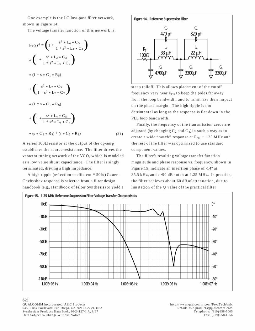
8-25QUALCOMM Incorporated, ASIC Products http://www.qualcomm.com/ProdTech/asic6455 Lusk Boulevard, San Diego, CA 92121-2779, USA E-mail: [email protected] Products Data Book, 80-24127-1 A, 8/97 Telephone: (619) 658-5005Data Subject to Change Without Notice Fax: (619) 658-1556
One example is the LC low-pass filter network,
shown in Figure 14.
The voltage transfer function of this network is:
(31)
A series 100Ω resistor at the output of the op-amp
establishes the source resistance. The filter drives the
varactor tuning network of the VCO, which is modeled
as a low value shunt capacitance. The filter is singly
terminated, driving a high impedance.
A high ripple (reflection coefficient = 50%) Cauer-
Chebyshev response is selected from a filter design
handbook (e.g., Handbook of Filter Synthesis) to yield a
FR(s)-1 = (1 +
* (1 +
* (1 + s * C1 * RS)
+ (
* (1 + s * C1 * RS)
+ (1 +
* (s * C3 * RS) + (s * C5 * RS)
s2 * L4 * C5
1 + s2 * L4 * C4)
s2 * L2 * C3
1 + s2 * L2 * C2)
s2 * L4 * C5
1 + s2 * L4 * C4)
s2 * L2 * C5
1 + s2 * L2 * C2)
Figure 14. Reference Suppression Filter
RS
100Ω
C2
470 pF
L2
33 µHL4
22 µH
C4
820 pF
C1
4700pFC3
3300pFC5
3300pF
steep rolloff. This allows placement of the cutoff
frequency very near FPD to keep the poles far away
from the loop bandwidth and to minimize their impact
on the phase margin. The high ripple is not
detrimental as long as the response is flat down in the
PLL loop bandwidth.
Finally, the frequency of the transmission zeros are
adjusted (by changing C2 and C4) in such a way as to
create a wide “notch” response at FPD = 1.25 MHz and
the rest of the filter was optimized to use standard
component values.
The filter’s resulting voltage transfer function
magnitude and phase response vs. frequency, shown in
Figure 15, indicate an insertion phase of -14° at
35.5 kHz, and a -90 dB notch at 1.25 MHz. In practice,
the filter achieves about 60 dB of attenuation, due to
limitation of the Q-value of the practical filter
1.00E+03 Hz 1.00E+04 Hz 1.00E+05 Hz 1.00E+06 Hz 1.00E+07 Hz
10dB
-10dB
-30dB
-50dB
-70dB
-90dB
-110dB
0°
-10°
-20°
-30°
-40°
-50°
-60°
Figure 15. 1.25 MHz Reference Suppression Filter Voltage Transfer Characteristics
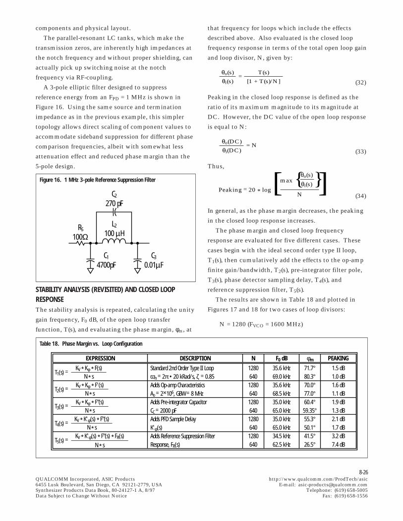
8-26QUALCOMM Incorporated, ASIC Products http://www.qualcomm.com/ProdTech/asic6455 Lusk Boulevard, San Diego, CA 92121-2779, USA E-mail: [email protected] Products Data Book, 80-24127-1 A, 8/97 Telephone: (619) 658-5005Data Subject to Change Without Notice Fax: (619) 658-1556
that frequency for loops which include the effects
described above. Also evaluated is the closed loop
frequency response in terms of the total open loop gain
and loop divisor, N, given by:
(32)
Peaking in the closed loop response is defined as the
ratio of its maximum magnitude to its magnitude at
DC. However, the DC value of the open loop response
is equal to N:
(33)
Thus,
(34)
In general, as the phase margin decreases, the peaking
in the closed loop response increases.
The phase margin and closed loop frequency
response are evaluated for five different cases. These
cases begin with the ideal second order type II loop,
T1(s), then cumulatively add the effects to the op-amp
finite gain/bandwidth, T2(s), pre-integrator filter pole,
T3(s), phase detector sampling delay, T4(s), and
reference suppression filter, T5(s).
The results are shown in Table 18 and plotted in
Figures 17 and 18 for two cases of loop divisors:
N = 1280 (FVCO = 1600 MHz)
KV * Kφ * F(s)N * s
KV * Kφ * F'(s)N * s
KV * Kφ * F"(s)N * s
KV * K'φ(s) * F"(s)N * s
KV * K'φ(s) * F"(s) * FR(s)N * s
T1(s) =
T2(s) =
T3(s) =
T4(s) =
T5(s) =
EXPRESSION DESCRIPTION
Standard 2nd Order Type II Loopωn = 2π • 20 kRad/s, ζ = 0.85Adds Op-amp CharacteristicsAo = 2×10⁶, GBW = 8 MHzAdds Pre-integrator CapacitorCC = 2000 pFAdds PFD Sample DelayK'φ(s)Adds Reference Suppression FilterResponse, FR(s)
N
1280640
1280640
1280640
1280640
1280640
F0 dB
35.6 kHz69.0 kHz35.6 kHz68.5 kHz35.0 kHz65.0 kHz35.0 kHz65.0 kHz34.5 kHz62.5 kHz
φm
71.7°80.3°70.0°77.0°60.4°
59.35°55.3°50.1°41.5°26.5°
PEAKING
1.5 dB1.0 dB1.6 dB1.1 dB1.9 dB1.3 dB2.1 dB1.7 dB3.2 dB7.4 dB
components and physical layout.
The parallel-resonant LC tanks, which make the
transmission zeros, are inherently high impedances at
the notch frequency and without proper shielding, can
actually pick up switching noise at the notch
frequency via RF-coupling.
A 3-pole elliptic filter designed to suppress
reference energy from an FPD = 1 MHz is shown in
Figure 16. Using the same source and termination
impedance as in the previous example, this simpler
topology allows direct scaling of component values to
accommodate sideband suppression for different phase
comparison frequencies, albeit with somewhat less
attenuation effect and reduced phase margin than the
5-pole design.
STABILITY ANALYSIS (REVISITED) AND CLOSED LOOPRESPONSEThe stability analysis is repeated, calculating the unity
gain frequency, F0 dB, of the open loop transfer
function, T(s), and evaluating the phase margin, φm, at
Figure 16. 1 MHz 3-pole Reference Suppression Filter
RS
100Ω
C2
270 pF
L2
100 µH
C1
4700pFC3
0.01µF
θo(s)
θi(s)=
T(s)
[1 + T(s)/N]
θo(DC)
θi(DC)= N
Peaking = 20 * log [ ]max θo(s)
θi(s)
N
Table 18. Phase Margin vs. Loop Configuration
8-27QUALCOMM Incorporated, ASIC Products http://www.qualcomm.com/ProdTech/asic6455 Lusk Boulevard, San Diego, CA 92121-2779, USA E-mail: [email protected] Products Data Book, 80-24127-1 A, 8/97 Telephone: (619) 658-5005Data Subject to Change Without Notice Fax: (619) 658-1556
90.0°
80.0°
70.0°
60.0°
50.0°
40.0°
30.0°
20.0°
10.0°
0.0°
60.0 dB
40.0 dB
20.0 dB
0.0 dB
-20.0 dB
-40.0 dB
-60.0 dB
-80.0 dB1.00E + 03 Hz 1.00E + 04 Hz 1.00E + 05 Hz 1.00E + 06 Hz
Frequency
N = 1280
90.0°
80.0°
70.0°
60.0°
50.0°
40.0°
30.0°
20.0°
10.0°
0.0°
60.0 dB
40.0 dB
20.0 dB
0.0 dB
-20.0 dB
-40.0 dB
-60.0 dB
-80.0 dB1.00E + 03 Hz 1.00E + 04 Hz 1.00E + 05 Hz 1.00E + 06 Hz
Frequency
N = 640
i=1i=2
i=3
i=4
i=5 i=5
i=1,2i=3,4
φm(S)
Ti (S)
i=1i=2
i=3
i=4
i=5i=5
i=1,2
i=3,4
Ti (S)
Figure 17. Bode Analysis - Open Loop Gain and Phase Margin
and, N = 640 (FVCO = 800 MHz)
First, at the lower end of the synthesizer output
frequency range, 800 MHz, N decreases by a factor of 2
to 640. On inspecting (13) and (14) it is clear that both
ωn and ζ increase by a factor of 2 . A recollection of
servo theory on a second type II loop suggests that an
increase in damping always improves the phase margin
and, hence, the stability of the loop. The results show
that for this ideal case the phase margin increases from
φm = 71.7° at F0 dB = 35.6 kHz at N = 1280 to φm =
80.3° at F0 dB = 69.0 kHz at N = 640. As expected, the
peaking drops from 1.5 dB to 1.0 dB.
For the case of T2(s), the op-amp finite gain/
bandwidth effects degrade the phase margin by 1.7°,where φm = 70.0° for N = 1280. Where N = 640, the
phase margin is degraded by 3.3° with φm = 77.0°.With the incorporation of the pre-integrator filter,
8-28QUALCOMM Incorporated, ASIC Products http://www.qualcomm.com/ProdTech/asic6455 Lusk Boulevard, San Diego, CA 92121-2779, USA E-mail: [email protected] Products Data Book, 80-24127-1 A, 8/97 Telephone: (619) 658-5005Data Subject to Change Without Notice Fax: (619) 658-1556
66.0 dB
64.0 dB
62.0 dB
60.0 dB
58.0 dB
56.0 dB
54.0 dB
52.0 dB1.00E + 03 Hz 1.00E + 04 Hz 1.00E + 05 Hz
Frequency
i=1
i=2
i=3
i=1
i=2
i=4
i=5
i=5
i=4
i=3
N=640 (800 MHz)
N=1280 (1600 MHz)
Figure 18. Closed Loop Frequency Response
the results for T3(s) show a more pronounced impact
on the phase margin and peaking.
When the phase detector sampling delay is added, it
is evident that although it does not effect the
magnitude of the open loop gain, T4(s), the phase
margin is degraded by the added phase delay of 9.4° at
the unity gain frequency, F0 dB = 65.0 kHz, for N = 640,
and 5.1° at F0 dB = 35.0 kHz, for N = 1280.
Up to this point, the results of this example have
indicated that although the added poles and delays
have begun to impact the phase margin and induce
peaking in the closed-loop frequency response, the loop
is still behaving approximately like the second order
loop in that for the larger ωn and ζ in the N = 640 case,
8-29QUALCOMM Incorporated, ASIC Products http://www.qualcomm.com/ProdTech/asic6455 Lusk Boulevard, San Diego, CA 92121-2779, USA E-mail: [email protected] Products Data Book, 80-24127-1 A, 8/97 Telephone: (619) 658-5005Data Subject to Change Without Notice Fax: (619) 658-1556
the phase margin and peaking are less. This is due to
the fact that up to this point, the pole and zero of the
loop filter, R1 * C and R2 * C, are still dominating the
response.
However, this is not the general case. For example,
if the loop bandwidth were higher, it would require
more gain out of the op-amp (larger R2/R1 ratio), and
the op-amp pole would be more dominant. Also, the
pre-integrator pole and detector sampling delays would
be relatively higher and thus have more impact.
Finally, the results show that by adding the
reference suppression filter in T5 (s), the impact on the
phase margin and peaking is quite severe in both cases,
φm = 41.5° for N = 1280, and φm = 26.5° for N = 640.
It is extremely important to note that the impact is
more pronounced for the case N = 640 (see Figure 18).
This is significant in that it contradicts the results of
the second loop theory. This is caused by the loop no
longer approximating the second order loop. In fact,
the higher order effects cause the natural loop
bandwidth and damping to lose their meaning in terms
of loop stability.
Although the phase margin of 41.5° at FVCO = 1600
MHz (N = 1280) is still acceptable, the results at N =
640 pose a few problems when operating at the
frequency FVCO = 800 MHz.
First, the low phase margin of 26.5° is not enough to
allow for component tolerances and drift due to age,
temperature, etc. Therefore, under some conditions
the loop could become unstable and lose lock
completely.
Also, the high amount of peaking (7.4 dB) in the
closed loop response corresponds to a higher
“overshoot” in the transient response of the loop. For
the loop to remain linear in operation, the VCO must
have a wider tuning range, and the loop amplifier must
have a wider dynamic range in order to accommodate
for this overshoot.
Finally, this excessive peaking in the loop frequency
response amplifies both the VCO and reference phase
noise contributions at frequency offsets where the
peaking occurs. Therefore, it can heavily degrade the
expected phase noise performance at those frequencies.
In summary, the results show that the cumulative
effects of all these additional factors greatly degrades
the stability when compared with an ideal second
order loop. Therefore, a different design approach is in
order when operating over the entire frequency range
FVCO = 800 -1600 MHz. For example, using a reference
suppression filter technique which has less insertion
phase, such as a third order LC, or a twin T notch at
1.25 MHz would reduce its insertion phase delay,
although it may require in-circuit tuning to achieve
adequate rejection. Alternatively, the effect of
decreasing N in the loop gain could be equalized by
non-linearizing the VCO tuning sensitivity over the
frequency range.
SYNTHESIZER OUTPUT SPECTRUMFigure 11a shows the output spectrum of a synthesizer
programmed to 1598.75 MHz (N = 1279) at a span of 5
MHz, indicating the 1.25 MHz reference spurious
outputs are less than -74 dBc.
At frequency offsets less than the loop bandwidth,
the synthesizer output phase noise consists of the
reference phase noise, the Q3236 frequency divider/
phase detector noise floor and the op-amp active loop
filter’s noise, all multiplied up by the loop divisor:
N = 1279 or 20 * log10(N) = 62 dB
Figure 11b shows the synthesizer output phase noise
measured in a 1 kHz bandwidth at frequency offsets up
to 100 kHz. The plot shows that at a 20 kHz offset,
the output phase noise is about -87 dBc/Hz. The
Q3236 phase noise contribution at that offset is less
than or equal to :
-87 - 62 = -149 dBc/Hz @ 20 kHz
The Q3236 PLL is an ECL device. This calculation
substantiates a phase noise floor of an ECL device to be
> -150 dBc.
8-30QUALCOMM Incorporated, ASIC Products http://www.qualcomm.com/ProdTech/asic6455 Lusk Boulevard, San Diego, CA 92121-2779, USA E-mail: [email protected] Products Data Book, 80-24127-1 A, 8/97 Telephone: (619) 658-5005Data Subject to Change Without Notice Fax: (619) 658-1556
question. In this way, maximizing the noise immunity
will help in achieving optimum phase noise results.
The Q3236 bus interface is double-buffered, which aids
in this isolation. Also, the device pinout is configured
so that all the digital inputs are on one side of the
package, allowing partitioning between the digital and
analog portions of the printed circuit board layout.
Additionally, the Q3236 contains on-chip bandgap
voltage referencing which is effective for filtering noise
below approximately 30 kHz when the power supply
requirement of VCC = +5.0 ± 0.5 V is met. To limit the
AM to PM conversion phase noise at higher
frequencies, it is essential to add external power supply
filtering.
First, the VCC inputs should each be bypassed to
ground with about a 0.01 µF capacitor. To simplify
circuit layout, these pins can be connected together
underneath the Q3236 package on the PWB. The +5 V
can run off of the same +5 V logic supply; but
depending on the level and frequencies of switching
noise on that supply, it may be desirable to insert a
series RF choke before the VCC inputs, which can
handle 75 mA.
For optimal synthesizer noise performance, it is
recommended to use a linear regulated power supply to
eliminate any contribution of extraneous noise
coupling through the power bus lines to the
synthesizer’s output.
The phase detector outputs should be considered
separately. There are five emitter follower outputs on
the Q3236: the VCO divider output, VCO DIV OUT,
the Lock Detect integrated output, CEXT, the double-
ended phase detector outputs, PD U OUT and PD D
OUT, and the reference divider output REF DIV OUT.
The outputs have separate supply rails brought off of
the Q3236. Specifically, VCCO1 is the VCO DIV OUT
and CEXT supply rail and VCCO2 is the supply rail for
PD U OUT, PD D OUT and REF DIV OUT. These
outputs are each externally terminated to ground with
510 Ω (except CEXT) and therefore draw 9 mA from its
supply rail. Since REF DIV OUT and VCO DIV OUT
are brought off-chip with their own output drivers,
they can be used to drive AC-coupled 50 Ω test and
measurement equipment or, of course, into other ECL
FREQUENCY SYNTHESIZER DESIGN CONSIDERATIONSWITH THE Q3236GENERAL ELECTROMAGNETIC ISSUESProper power supply biasing and grounding are critical
to the design of frequency synthesizers for high
performance communications systems. Power supply
and digital bus noise can couple into the PLL circuitry
and degrade phase noise performance. Additionally,
PLL divider switching noise and phase detector pulses
coupling onto power supply lines can create EMI
problems and couple into high-gain/wideband IF
amplifier chains.
The Q3236 offers some key advantages in these
areas due to its highly integrated architecture. In the
Q3236 synthesizer, all the high speed digital circuitry
is confined to a small area and the internal logic is
implemented with lower bias currents due to a high ft
process, and uses fully differential CML circuits. Both
of these features reduce the amount of switching noise
on the power supply inputs. This can be compared
with a discrete, distributed design which has long
circuit traces carrying fast switching logic signals
requiring special terminations. The discrete approach
also allows a greater opportunity for picking up
external noise which can degrade the synthesizer’s
phase noise performance. The Q3236 architecture and
pinout are optimized for simple and compact external
circuit layout which aids in these issues. However,
there are still some important guidelines to follow.
When programming a PLL synthesizer using a
digital microprocessor bus, it is desirable to isolate the
bus from the frequency divider/phase detector circuitry
because it is usually switching all the time and can add
noise to the synthesizer. If, for instance, the HOP WR,
M1 WR, M2 WR, and AWR signals are being controlled
by logic that is very noisy or perhaps goes to a high
impedance state when the signals are de-selected, the
connecting traces can easily pick up extraneous signals
which RF-couple to the output and become another
component of low-level additive phase noise. The data
bus inputs can also be susceptible in this way. One
way to mitigate this so called noise feedthru effect is
to put high-frequency bypass capacitors, such as 100 pF
value, right at the PLL control interface pins in
8-31QUALCOMM Incorporated, ASIC Products http://www.qualcomm.com/ProdTech/asic6455 Lusk Boulevard, San Diego, CA 92121-2779, USA E-mail: [email protected] Products Data Book, 80-24127-1 A, 8/97 Telephone: (619) 658-5005Data Subject to Change Without Notice Fax: (619) 658-1556
logic. It is sometimes useful to shift CEXT’s internal
out-of-lock threshold closer to either the ECL 2 V
“High” or “Low” state in order to establish a more
consistent threshold to trigger LD OUT between
unlocked and locked conditions, depending on the
response of the integrated waveform on CEXT. This is
done by connecting a resistor (typical values between
20 kΩ to 50 kΩ) from the CEXT output to either +5
Volts or ground, depending on which direction of bias
is desired.
Because emitter follower outputs are always “On”,
any power supply ripple or switching noise on the
supply rail goes directly through to the phase detector
output and therefore can increase the phase noise and
spurious output of the synthesizer. Furthermore, the
phase detector outputs convey phase error information
in the form of very narrow 2 V pulses. If not dealt
with, these pulses bleed into the power supply and
corrupt the system. If REF DIV OUT or VCO DIV
OUT are only going to be used as a test point for high
impedance probing, such as for monitoring the pulse-
train waveform with an oscilloscope probe, then these
outputs can be externally terminated with a higher
value resistor, such as 10 KΩ. This can benefit in a
couple of ways, especially for very densely populated
circuit layout conditions. First, it reduces the current
draw of either output from 9 mA to under 0.5 mA
Secondly, it will cause a lower level of signal current to
radiate which reduces another additive component to
potentially degrade the output phase noise.
Therefore, it may be necessary to connect the phase
detector supply rail, VCCO2, to a separate, well-filtered
supply. The filtering should consist of a 0.01 µF bypass
capacitor followed by a ladder of series inductor and
shunt capacitor elements whose values can effectively
filter the frequencies. For instance, inductors of 100
µH combined with 47 µF electrolytic capacitors
effectively filter noise in the tens of kHz but are not
effective at higher frequencies. At these higher
frequencies, 0.01 µF capacitors along with ferrite beads
are effective.
Finally, ground plane construction is very
important. Its quality directly impacts the
effectiveness of the filtering/bypassing techniques. By
taking advantage of the Q3236 pinout arrangement,
and using surface mount components on a two-layer
printed circuit board, it is possible to achieve a
virtually solid ground plane under the device. The
ground plane can also be utilized to act as a coaxial-
like shield to prevent parallel-line coupling between
the VCO input and the digital input traces. Coupling
of this kind can degrade VCO input VSWR and EMI
immunity which can be detrimental to the
synthesizer’s noise performance. Surrounding the
VCO input trace with a “shield plane” of copper on the
top layer, connected to the ground plane with a row of
vias, should provide such a shielding effect.
VCO AND REFERENCE LINE RECEIVER INPUT MINIMUM EDGERATESAlthough the device operates for sinusoidal VCO and
reference input signals below 20 MHz, the sensitivity
is reduced. There is a minimum edge-rate, which
corresponds to about 200 mV in one half cycle of a
20 MHz sinusoid (25 ns). Therefore, the input
frequency range extends down to DC with input
waveforms whose amplitudes are at least 200 mVpp
and rise/fall times are less than 25 ns. For larger
amplitudes, the rise/fall times can be slower as long as
they correspond to about 200 mV/25 ns.
This is easily understood considering that the
frequency divider is an edge-triggered circuit, which
depends on the transition of the clock signal through a
certain level threshold (also known as a zero-crossing).
There is an inherent amplitude-to-phase noise
conversion process associated with edge-triggered
circuits. Amplitude noise on the clock signal during
this transition causes an uncertainty when the zero-
crossing occurred, resulting in clock edge jitter.
Random jitter on the clock edges converts to phase
noise in the synthesizer. Furthermore, a given amount
of AM noise will cause more edge jitter on a clock
which has slower edges (rise/fall times). The longer it
takes to pass through the zero-crossing threshold, the
more influence the AM noise will have on the zero
crossing.
For applications in which phase noise performance
is critical, the circuit in Figure 19 is recommended for
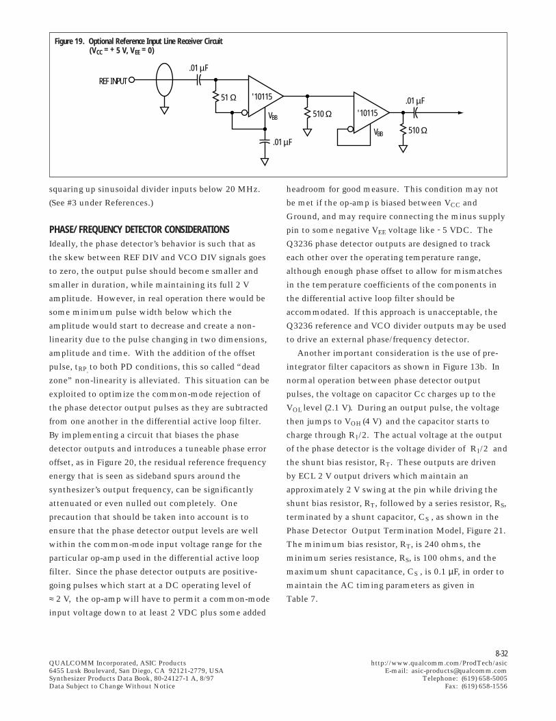
8-32QUALCOMM Incorporated, ASIC Products http://www.qualcomm.com/ProdTech/asic6455 Lusk Boulevard, San Diego, CA 92121-2779, USA E-mail: [email protected] Products Data Book, 80-24127-1 A, 8/97 Telephone: (619) 658-5005Data Subject to Change Without Notice Fax: (619) 658-1556
squaring up sinusoidal divider inputs below 20 MHz.
(See #3 under References.)
PHASE/FREQUENCY DETECTOR CONSIDERATIONSIdeally, the phase detector’s behavior is such that as
the skew between REF DIV and VCO DIV signals goes
to zero, the output pulse should become smaller and
smaller in duration, while maintaining its full 2 V
amplitude. However, in real operation there would be
some minimum pulse width below which the
amplitude would start to decrease and create a non-
linearity due to the pulse changing in two dimensions,
amplitude and time. With the addition of the offset
pulse, tRP, to both PD conditions, this so called “dead
zone” non-linearity is alleviated. This situation can be
exploited to optimize the common-mode rejection of
the phase detector output pulses as they are subtracted
from one another in the differential active loop filter.
By implementing a circuit that biases the phase
detector outputs and introduces a tuneable phase error
offset, as in Figure 20, the residual reference frequency
energy that is seen as sideband spurs around the
synthesizer’s output frequency, can be significantly
attenuated or even nulled out completely. One
precaution that should be taken into account is to
ensure that the phase detector output levels are well
within the common-mode input voltage range for the
particular op-amp used in the differential active loop
filter. Since the phase detector outputs are positive-
going pulses which start at a DC operating level of
≈ 2 V, the op-amp will have to permit a common-mode
input voltage down to at least 2 VDC plus some added
headroom for good measure. This condition may not
be met if the op-amp is biased between VCC and
Ground, and may require connecting the minus supply
pin to some negative VEE voltage like - 5 VDC. The
Q3236 phase detector outputs are designed to track
each other over the operating temperature range,
although enough phase offset to allow for mismatches
in the temperature coefficients of the components in
the differential active loop filter should be
accommodated. If this approach is unacceptable, the
Q3236 reference and VCO divider outputs may be used
to drive an external phase/frequency detector.
Another important consideration is the use of pre-
integrator filter capacitors as shown in Figure 13b. In
normal operation between phase detector output
pulses, the voltage on capacitor Cc charges up to the
VOL level (2.1 V). During an output pulse, the voltage
then jumps to VOH (4 V) and the capacitor starts to
charge through R1/2. The actual voltage at the output
of the phase detector is the voltage divider of R1/2 and
the shunt bias resistor, RT. These outputs are driven
by ECL 2 V output drivers which maintain an
approximately 2 V swing at the pin while driving the
shunt bias resistor, RT, followed by a series resistor, RS,
terminated by a shunt capacitor, CS , as shown in the
Phase Detector Output Termination Model, Figure 21.
The minimum bias resistor, RT, is 240 ohms, the
minimum series resistance, RS, is 100 ohms, and the
maximum shunt capacitance, CS , is 0.1 µF, in order to
maintain the AC timing parameters as given in
Table 7.
Figure 19. Optional Reference Input Line Receiver Circuit (VCC = + 5 V, VEE = 0)
REF INPUT
.01 µF
.01 µF51 Ω
.01 µF
510 Ω
510 Ω
'10115
'10115VBB
VBB
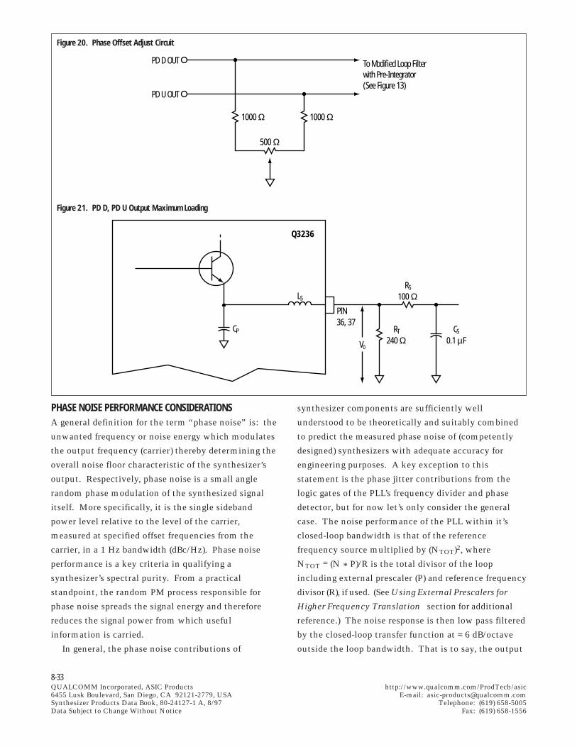
8-33QUALCOMM Incorporated, ASIC Products http://www.qualcomm.com/ProdTech/asic6455 Lusk Boulevard, San Diego, CA 92121-2779, USA E-mail: [email protected] Products Data Book, 80-24127-1 A, 8/97 Telephone: (619) 658-5005Data Subject to Change Without Notice Fax: (619) 658-1556
PHASE NOISE PERFORMANCE CONSIDERATIONSA general definition for the term “phase noise” is: the
unwanted frequency or noise energy which modulates
the output frequency (carrier) thereby determining the
overall noise floor characteristic of the synthesizer’s
output. Respectively, phase noise is a small angle
random phase modulation of the synthesized signal
itself. More specifically, it is the single sideband
power level relative to the level of the carrier,
measured at specified offset frequencies from the
carrier, in a 1 Hz bandwidth (dBc/Hz). Phase noise
performance is a key criteria in qualifying a
synthesizer’s spectral purity. From a practical
standpoint, the random PM process responsible for
phase noise spreads the signal energy and therefore
reduces the signal power from which useful
information is carried.
In general, the phase noise contributions of
synthesizer components are sufficiently well
understood to be theoretically and suitably combined
to predict the measured phase noise of (competently
designed) synthesizers with adequate accuracy for
engineering purposes. A key exception to this
statement is the phase jitter contributions from the
logic gates of the PLL’s frequency divider and phase
detector, but for now let’s only consider the general
case. The noise performance of the PLL within it’s
closed-loop bandwidth is that of the reference
frequency source multiplied by (NTOT)2, where
NTOT = (N * P)/R is the total divisor of the loop
including external prescaler (P) and reference frequency
divisor (R), if used. (See Using External Prescalers for
Higher Frequency Translation section for additional
reference.) The noise response is then low pass filtered
by the closed-loop transfer function at ≈ 6 dB/octave
outside the loop bandwidth. That is to say, the output
Q3236
V0
RS
100 ΩLS
RT
240 ΩCS
0.1 µF
PIN36, 37
CP
PD D OUT
PD U OUT
1000 Ω 1000 Ω
500 Ω
To Modified Loop Filterwith Pre-Integrator(See Figure 13)
Figure 20. Phase Offset Adjust Circuit
Figure 21. PD D, PD U Output Maximum Loading
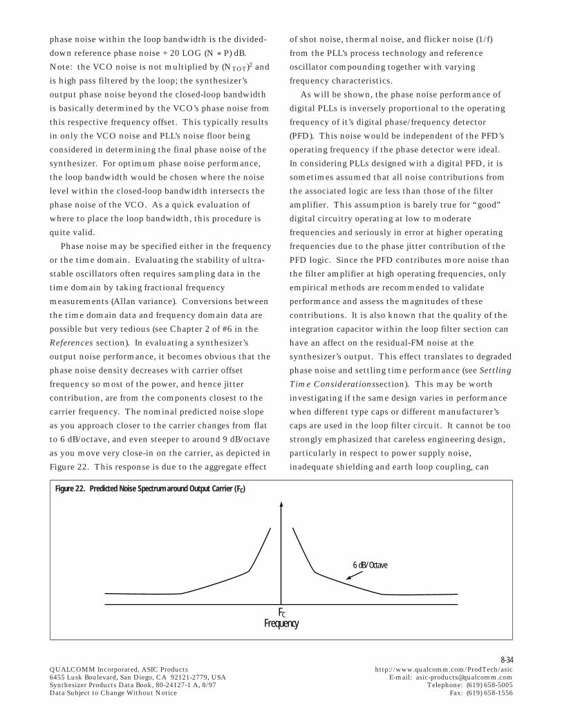
8-34QUALCOMM Incorporated, ASIC Products http://www.qualcomm.com/ProdTech/asic6455 Lusk Boulevard, San Diego, CA 92121-2779, USA E-mail: [email protected] Products Data Book, 80-24127-1 A, 8/97 Telephone: (619) 658-5005Data Subject to Change Without Notice Fax: (619) 658-1556
phase noise within the loop bandwidth is the divided-
down reference phase noise + 20 LOG (N * P) dB.
Note: the VCO noise is not multiplied by (NTOT)2 and
is high pass filtered by the loop; the synthesizer’s
output phase noise beyond the closed-loop bandwidth
is basically determined by the VCO’s phase noise from
this respective frequency offset. This typically results
in only the VCO noise and PLL’s noise floor being
considered in determining the final phase noise of the
synthesizer. For optimum phase noise performance,
the loop bandwidth would be chosen where the noise
level within the closed-loop bandwidth intersects the
phase noise of the VCO. As a quick evaluation of
where to place the loop bandwidth, this procedure is
quite valid.
Phase noise may be specified either in the frequency
or the time domain. Evaluating the stability of ultra-
stable oscillators often requires sampling data in the
time domain by taking fractional frequency
measurements (Allan variance). Conversions between
the time domain data and frequency domain data are
possible but very tedious (see Chapter 2 of #6 in the
References section). In evaluating a synthesizer’s
output noise performance, it becomes obvious that the
phase noise density decreases with carrier offset
frequency so most of the power, and hence jitter
contribution, are from the components closest to the
carrier frequency. The nominal predicted noise slope
as you approach closer to the carrier changes from flat
to 6 dB/octave, and even steeper to around 9 dB/octave
as you move very close-in on the carrier, as depicted in
Figure 22. This response is due to the aggregate effect
of shot noise, thermal noise, and flicker noise (1/f)
from the PLL’s process technology and reference
oscillator compounding together with varying
frequency characteristics.
As will be shown, the phase noise performance of
digital PLLs is inversely proportional to the operating
frequency of it’s digital phase/frequency detector
(PFD). This noise would be independent of the PFD’s
operating frequency if the phase detector were ideal.
In considering PLLs designed with a digital PFD, it is
sometimes assumed that all noise contributions from
the associated logic are less than those of the filter
amplifier. This assumption is barely true for “good”
digital circuitry operating at low to moderate
frequencies and seriously in error at higher operating
frequencies due to the phase jitter contribution of the
PFD logic. Since the PFD contributes more noise than
the filter amplifier at high operating frequencies, only
empirical methods are recommended to validate
performance and assess the magnitudes of these
contributions. It is also known that the quality of the
integration capacitor within the loop filter section can
have an affect on the residual-FM noise at the
synthesizer’s output. This effect translates to degraded
phase noise and settling time performance (see Settling
Time Considerations section). This may be worth
investigating if the same design varies in performance
when different type caps or different manufacturer’s
caps are used in the loop filter circuit. It cannot be too
strongly emphasized that careless engineering design,
particularly in respect to power supply noise,
inadequate shielding and earth loop coupling, can
Figure 22. Predicted Noise Spectrum around Output Carrier (FC)
6 dB/Octave
FCFrequency
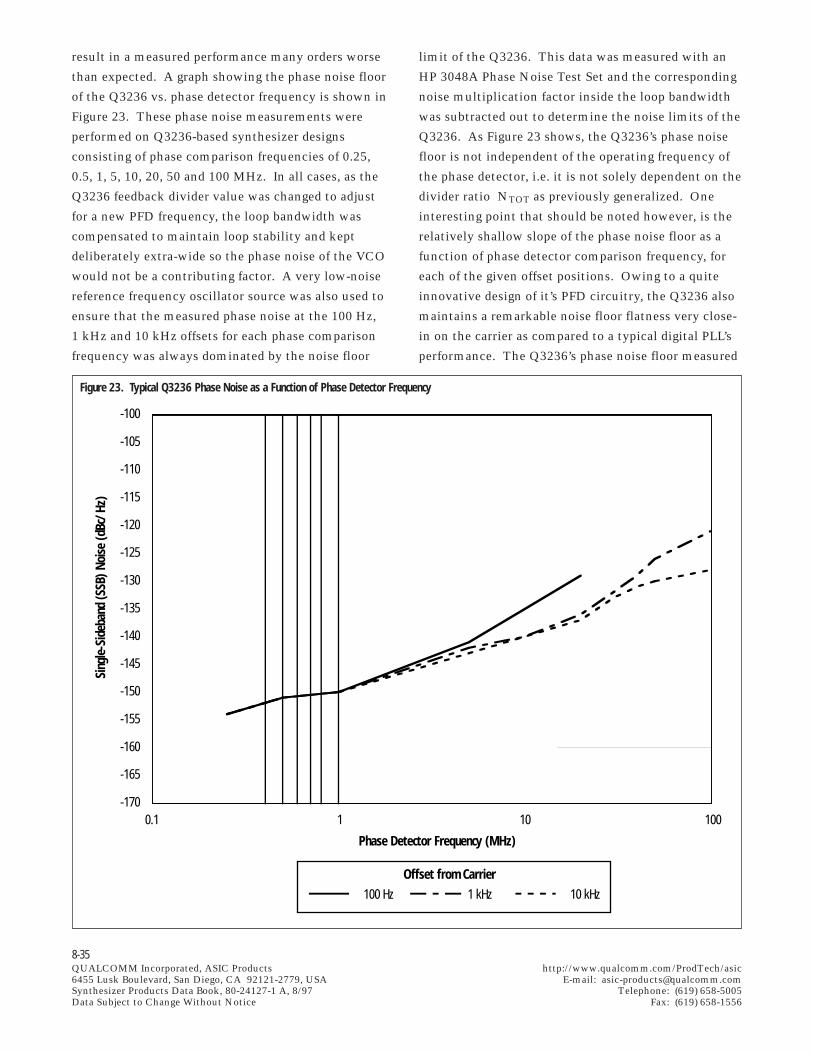
8-35QUALCOMM Incorporated, ASIC Products http://www.qualcomm.com/ProdTech/asic6455 Lusk Boulevard, San Diego, CA 92121-2779, USA E-mail: [email protected] Products Data Book, 80-24127-1 A, 8/97 Telephone: (619) 658-5005Data Subject to Change Without Notice Fax: (619) 658-1556
result in a measured performance many orders worse
than expected. A graph showing the phase noise floor
of the Q3236 vs. phase detector frequency is shown in
Figure 23. These phase noise measurements were
performed on Q3236-based synthesizer designs
consisting of phase comparison frequencies of 0.25,
0.5, 1, 5, 10, 20, 50 and 100 MHz. In all cases, as the
Q3236 feedback divider value was changed to adjust
for a new PFD frequency, the loop bandwidth was
compensated to maintain loop stability and kept
deliberately extra-wide so the phase noise of the VCO
would not be a contributing factor. A very low-noise
reference frequency oscillator source was also used to
ensure that the measured phase noise at the 100 Hz,
1 kHz and 10 kHz offsets for each phase comparison
frequency was always dominated by the noise floor
limit of the Q3236. This data was measured with an
HP 3048A Phase Noise Test Set and the corresponding
noise multiplication factor inside the loop bandwidth
was subtracted out to determine the noise limits of the
Q3236. As Figure 23 shows, the Q3236’s phase noise
floor is not independent of the operating frequency of
the phase detector, i.e. it is not solely dependent on the
divider ratio NTOT as previously generalized. One
interesting point that should be noted however, is the
relatively shallow slope of the phase noise floor as a
function of phase detector comparison frequency, for
each of the given offset positions. Owing to a quite
innovative design of it’s PFD circuitry, the Q3236 also
maintains a remarkable noise floor flatness very close-
in on the carrier as compared to a typical digital PLL’s
performance. The Q3236’s phase noise floor measured
-170
-165
-160
-155
-150
-145
-140
-135
-130
-125
-120
-115
-110
-105
-100
0.1 1 10 100
Phase Detector Frequency (MHz)
Sing
le-Si
deba
nd (S
SB) N
oise
(dBc
/Hz)
100 Hz 1 kHz 10 kHz
Offset from Carrier
Figure 23. Typical Q3236 Phase Noise as a Function of Phase Detector Frequency
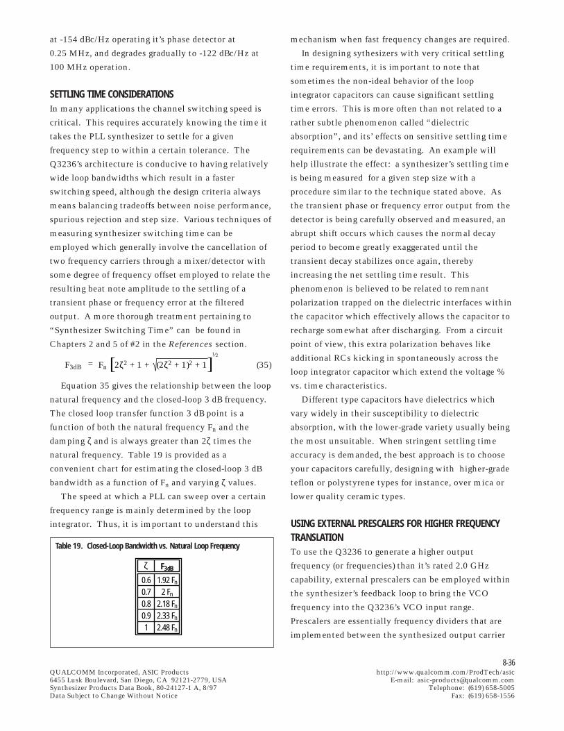
8-36QUALCOMM Incorporated, ASIC Products http://www.qualcomm.com/ProdTech/asic6455 Lusk Boulevard, San Diego, CA 92121-2779, USA E-mail: [email protected] Products Data Book, 80-24127-1 A, 8/97 Telephone: (619) 658-5005Data Subject to Change Without Notice Fax: (619) 658-1556
at -154 dBc/Hz operating it’s phase detector at
0.25 MHz, and degrades gradually to -122 dBc/Hz at
100 MHz operation.
SETTLING TIME CONSIDERATIONSIn many applications the channel switching speed is
critical. This requires accurately knowing the time it
takes the PLL synthesizer to settle for a given
frequency step to within a certain tolerance. The
Q3236’s architecture is conducive to having relatively
wide loop bandwidths which result in a faster
switching speed, although the design criteria always
means balancing tradeoffs between noise performance,
spurious rejection and step size. Various techniques of
measuring synthesizer switching time can be
employed which generally involve the cancellation of
two frequency carriers through a mixer/detector with
some degree of frequency offset employed to relate the
resulting beat note amplitude to the settling of a
transient phase or frequency error at the filtered
output. A more thorough treatment pertaining to
“Synthesizer Switching Time” can be found in
Chapters 2 and 5 of #2 in the References section.
(35)
Equation 35 gives the relationship between the loop
natural frequency and the closed-loop 3 dB frequency.
The closed loop transfer function 3 dB point is a
function of both the natural frequency Fn and the
damping ζ and is always greater than 2ζ times the
natural frequency. Table 19 is provided as a
convenient chart for estimating the closed-loop 3 dB
bandwidth as a function of Fn and varying ζ values.
The speed at which a PLL can sweep over a certain
frequency range is mainly determined by the loop
integrator. Thus, it is important to understand this
mechanism when fast frequency changes are required.
In designing sythesizers with very critical settling
time requirements, it is important to note that
sometimes the non-ideal behavior of the loop
integrator capacitors can cause significant settling
time errors. This is more often than not related to a
rather subtle phenomenon called “dielectric
absorption”, and its’ effects on sensitive settling time
requirements can be devastating. An example will
help illustrate the effect: a synthesizer’s settling time
is being measured for a given step size with a
procedure similar to the technique stated above. As
the transient phase or frequency error output from the
detector is being carefully observed and measured, an
abrupt shift occurs which causes the normal decay
period to become greatly exaggerated until the
transient decay stabilizes once again, thereby
increasing the net settling time result. This
phenomenon is believed to be related to remnant
polarization trapped on the dielectric interfaces within
the capacitor which effectively allows the capacitor to
recharge somewhat after discharging. From a circuit
point of view, this extra polarization behaves like
additional RCs kicking in spontaneously across the
loop integrator capacitor which extend the voltage %
vs. time characteristics.
Different type capacitors have dielectrics which
vary widely in their susceptibility to dielectric
absorption, with the lower-grade variety usually being
the most unsuitable. When stringent settling time
accuracy is demanded, the best approach is to choose
your capacitors carefully, designing with higher-grade
teflon or polystyrene types for instance, over mica or
lower quality ceramic types.
USING EXTERNAL PRESCALERS FOR HIGHER FREQUENCYTRANSLATIONTo use the Q3236 to generate a higher output
frequency (or frequencies) than it’s rated 2.0 GHz
capability, external prescalers can be employed within
the synthesizer’s feedback loop to bring the VCO
frequency into the Q3236’s VCO input range.
Prescalers are essentially frequency dividers that are
implemented between the synthesized output carrier
F3dB = Fn [2ζ2 + 1 + (2ζ2 + 1)2 + 1]1⁄2
ζ
0.60.70.80.91
F3dB
1.92 Fn
2 Fn
2.18 Fn
2.33 Fn
2.48 Fn
Table 19. Closed-Loop Bandwidth vs. Natural Loop Frequency
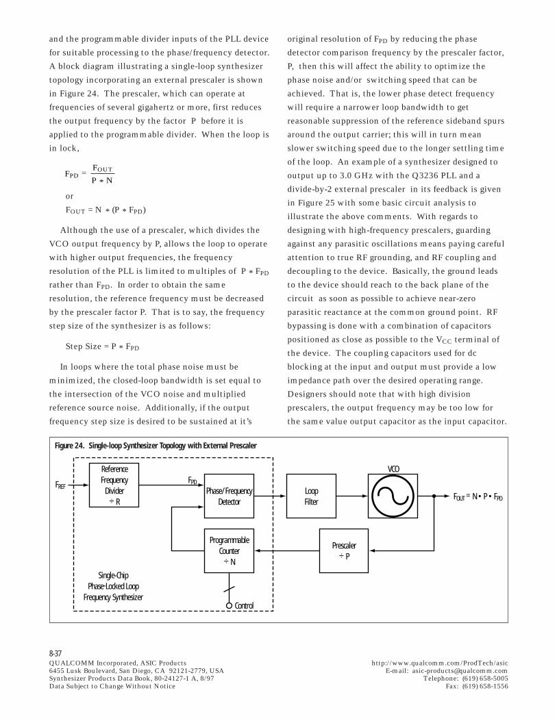
8-37QUALCOMM Incorporated, ASIC Products http://www.qualcomm.com/ProdTech/asic6455 Lusk Boulevard, San Diego, CA 92121-2779, USA E-mail: [email protected] Products Data Book, 80-24127-1 A, 8/97 Telephone: (619) 658-5005Data Subject to Change Without Notice Fax: (619) 658-1556
and the programmable divider inputs of the PLL device
for suitable processing to the phase/frequency detector.
A block diagram illustrating a single-loop synthesizer
topology incorporating an external prescaler is shown
in Figure 24. The prescaler, which can operate at
frequencies of several gigahertz or more, first reduces
the output frequency by the factor P before it is
applied to the programmable divider. When the loop is
in lock,
or
FOUT = N * (P * FPD)
Although the use of a prescaler, which divides the
VCO output frequency by P, allows the loop to operate
with higher output frequencies, the frequency
resolution of the PLL is limited to multiples of P * FPD
rather than FPD. In order to obtain the same
resolution, the reference frequency must be decreased
by the prescaler factor P. That is to say, the frequency
step size of the synthesizer is as follows:
Step Size = P * FPD
In loops where the total phase noise must be
minimized, the closed-loop bandwidth is set equal to
the intersection of the VCO noise and multiplied
reference source noise. Additionally, if the output
frequency step size is desired to be sustained at it’s
original resolution of FPD by reducing the phase
detector comparison frequency by the prescaler factor,
P, then this will affect the ability to optimize the
phase noise and/or switching speed that can be
achieved. That is, the lower phase detect frequency
will require a narrower loop bandwidth to get
reasonable suppression of the reference sideband spurs
around the output carrier; this will in turn mean
slower switching speed due to the longer settling time
of the loop. An example of a synthesizer designed to
output up to 3.0 GHz with the Q3236 PLL and a
divide-by-2 external prescaler in its feedback is given
in Figure 25 with some basic circuit analysis to
illustrate the above comments. With regards to
designing with high-frequency prescalers, guarding
against any parasitic oscillations means paying careful
attention to true RF grounding, and RF coupling and
decoupling to the device. Basically, the ground leads
to the device should reach to the back plane of the
circuit as soon as possible to achieve near-zero
parasitic reactance at the common ground point. RF
bypassing is done with a combination of capacitors
positioned as close as possible to the VCC terminal of
the device. The coupling capacitors used for dc
blocking at the input and output must provide a low
impedance path over the desired operating range.
Designers should note that with high division
prescalers, the output frequency may be too low for
the same value output capacitor as the input capacitor.
FREF
ReferenceFrequency
Divider÷ R
Phase/FrequencyDetector
LoopFilter
VCO
FOUT = N • P • FPD
ProgrammableCounter
÷ N
Prescaler÷ P
Control
FPD
Single-ChipPhase-Locked Loop
Frequency Synthesizer
FPD = FOUT
P * N
Figure 24. Single-loop Synthesizer Topology with External Prescaler
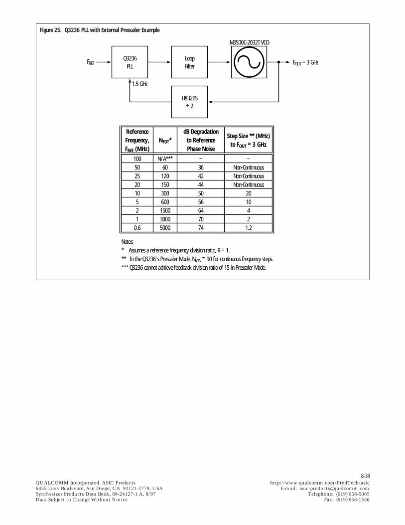
8-38QUALCOMM Incorporated, ASIC Products http://www.qualcomm.com/ProdTech/asic6455 Lusk Boulevard, San Diego, CA 92121-2779, USA E-mail: [email protected] Products Data Book, 80-24127-1 A, 8/97 Telephone: (619) 658-5005Data Subject to Change Without Notice Fax: (619) 658-1556
FREFQ3236
PLLLoopFilter
M3500C-2032T VCO
FOUT = 3 GHz
U832BS÷ 2
1.5 GHz
ReferenceFrequency,FREF (MHz)
10050252010521
0.6
NTOT*
N/A***60120150300600150030005000
dB Degradationto ReferencePhase Noise
–3642445056647074
Step Size ** (MHz)to FOUT = 3 GHz
–Non-ContinuousNon-ContinuousNon-Continuous
201042
1.2
Notes:* Assumes a reference frequency division ratio, R = 1.** In the Q3236's Prescaler Mode, NMIN = 90 for continuous frequency steps.*** Q3236 cannot achieve feedback division ratio of 15 in Prescaler Mode.
Figure 25. Q3236 PLL with External Prescaler Example
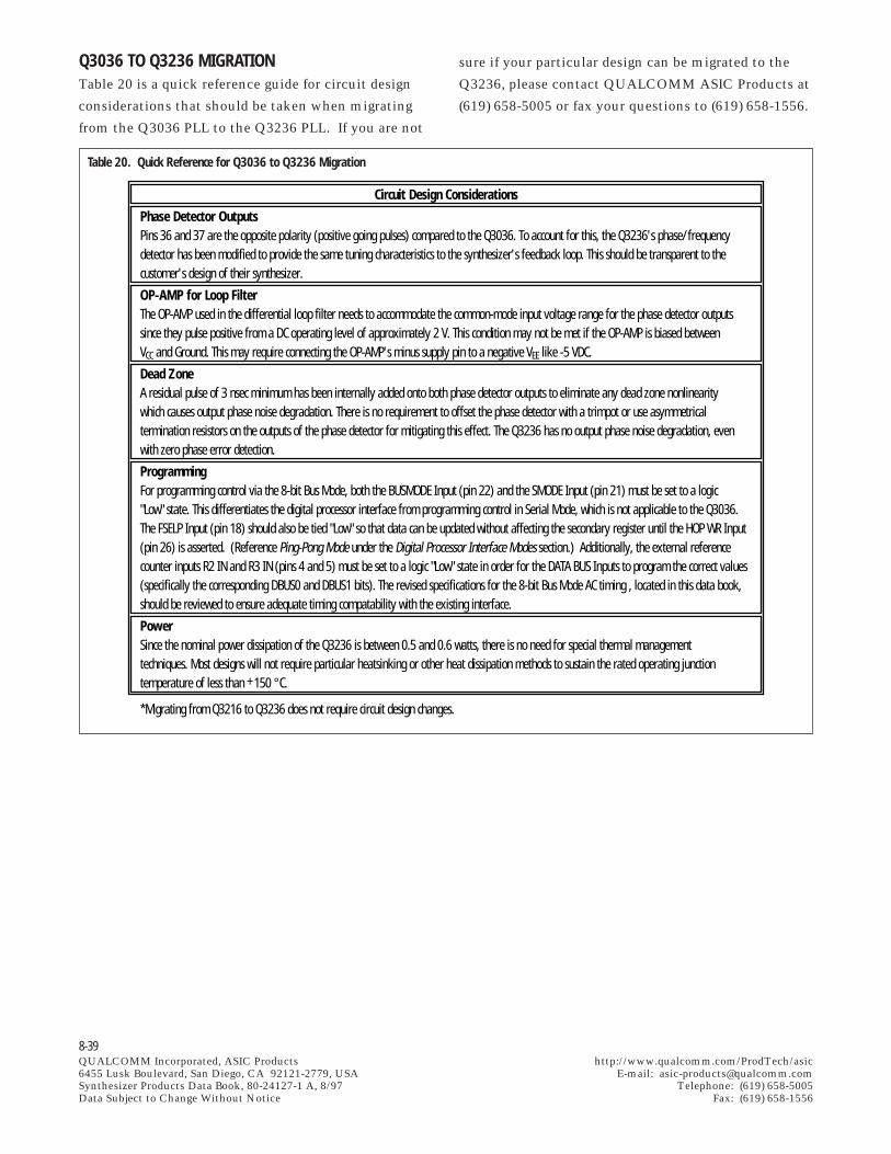
8-39QUALCOMM Incorporated, ASIC Products http://www.qualcomm.com/ProdTech/asic6455 Lusk Boulevard, San Diego, CA 92121-2779, USA E-mail: [email protected] Products Data Book, 80-24127-1 A, 8/97 Telephone: (619) 658-5005Data Subject to Change Without Notice Fax: (619) 658-1556
Table 20. Quick Reference for Q3036 to Q3236 Migration
Phase Detector OutputsPins 36 and 37 are the opposite polarity (positive going pulses) compared to the Q3036. To account for this, the Q3236's phase/frequency detector has been modified to provide the same tuning characteristics to the synthesizer's feedback loop. This should be transparent to thecustomer's design of their synthesizer.
OP-AMP for Loop FilterThe OP-AMP used in the differential loop filter needs to accommodate the common-mode input voltage range for the phase detector outputs since they pulse positive from a DC operating level of approximately 2 V. This condition may not be met if the OP-AMP is biased betweenVCC and Ground. This may require connecting the OP-AMP's minus supply pin to a negative VEE like -5 VDC.
Dead ZoneA residual pulse of 3 nsec minimum has been internally added onto both phase detector outputs to eliminate any dead zone nonlinearitywhich causes output phase noise degradation. There is no requirement to offset the phase detector with a trimpot or use asymmetricaltermination resistors on the outputs of the phase detector for mitigating this effect. The Q3236 has no output phase noise degradation, evenwith zero phase error detection.
ProgrammingFor programming control via the 8-bit Bus Mode, both the BUSMODE Input (pin 22) and the SMODE Input (pin 21) must be set to a logic"Low" state. This differentiates the digital processor interface from programming control in Serial Mode, which is not applicable to the Q3036.The FSELP Input (pin 18) should also be tied "Low" so that data can be updated without affecting the secondary register until the HOP WR Input(pin 26) is asserted. (Reference Ping-Pong Mode under the Digital Processor Interface Modes section.) Additionally, the external referencecounter inputs R2 IN and R3 IN (pins 4 and 5) must be set to a logic "Low" state in order for the DATA BUS Inputs to program the correct values(specifically the corresponding DBUS0 and DBUS1 bits). The revised specifications for the 8-bit Bus Mode AC timing , located in this data book,should be reviewed to ensure adequate timing compatability with the existing interface.
PowerSince the nominal power dissipation of the Q3236 is between 0.5 and 0.6 watts, there is no need for special thermal managementtechniques. Most designs will not require particular heatsinking or other heat dissipation methods to sustain the rated operating junctiontemperature of less than +150 °C.
*Migrating from Q3216 to Q3236 does not require circuit design changes.
Circuit Design Considerations
Q3036 TO Q3236 MIGRATIONTable 20 is a quick reference guide for circuit design
considerations that should be taken when migrating
from the Q3036 PLL to the Q3236 PLL. If you are not
sure if your particular design can be migrated to the
Q3236, please contact QUALCOMM ASIC Products at
(619) 658-5005 or fax your questions to (619) 658-1556.
8-40QUALCOMM Incorporated, ASIC Products http://www.qualcomm.com/ProdTech/asic6455 Lusk Boulevard, San Diego, CA 92121-2779, USA E-mail: [email protected] Products Data Book, 80-24127-1 A, 8/97 Telephone: (619) 658-5005Data Subject to Change Without Notice Fax: (619) 658-1556
Q0420 PLO EVALUATION SYSTEMThe Q0420 Phase-Locked Oscillator (PLO) Evaluation
System is a complete evaluation board designed on a
compact 5” x 7.5” printed circuit card for the Q3236
PLL. The actual evaluation platform includes a fixed
demonstration as well as a custom prototyping design.
A block diagram is shown in Figure 26. The Q0420
demonstration platform consists of a phase-locked
oscillator system which generates output frequencies
from 2 GHz to 3 GHz with a minimum step size of
5 MHz over the full output range (÷2 prescaler
included on-board). The custom prototyping option
allows the designer to rapidly configure a custom
synthesizer by adding the VCO, loop filter and
reference suppression filter components to the
alternative circuit sections of the board. The user can
easily select between the demonstration platform and
the custom prototyping design via on-board jumper
options. Additional input and output connectors are
also provided to easily support the use of off-board
VCOs and prescalers to quickly evaluate the
performance tradeoffs between alternative
components.
The Q0420 can be computer-controlled for remote
operation, or alternatively controlled through the on-
board frequency control switches for stand-alone
operation. The menu-driven software will
automatically compute all desired frequency
programming and can exercise the following Q3236
modes of operation:
• 16-bit Direct Parallel Control
• 8-bit Data Bus Control
• 20-bit Serial Control
• 8-bit Data Ping-Pong Control
• 20-bit Serial Ping-Pong Control
Stand-alone operation with the Q0420 requires only
the + 15 VDC power supply voltage, but can only
utilize the Q3236’s direct parallel interface for
frequency programming using on-board DIP switches.
The User’s Guide provides all the information
required to operate the Q0420 and exercise all built-in
functionality of the Q3236. Appendices are also
provided which contain the schematics, layout and
complete parts list. The Q0420 consists of a PLL
Evaluation Board, Control Software, Control Cable,
Digital I/O (DIO) Board and DIO Board Installation
Software. In order to operate the PLL Evaluation
Board, the DIO Board needs to be installed in a PC.
The DIO Driver Software and the Q0420 Control
Software need to be installed on the hard drive of the
PC. The Q0420 PLL Evaluation System requires the
following computer hardware as a minimum to operate
in Remote Mode:
• PC 80386 or Better
• 4 MB RAM
• Math Co-processor
• Hard Drive
• Mouse
• Windows™ Version 3.1 or Windows ‘95™
• SVGA Video Card (1024 X 768 Resolution, Small
Fonts)
Note: Windows™ is a trademark of Microsoft ®
Corporation
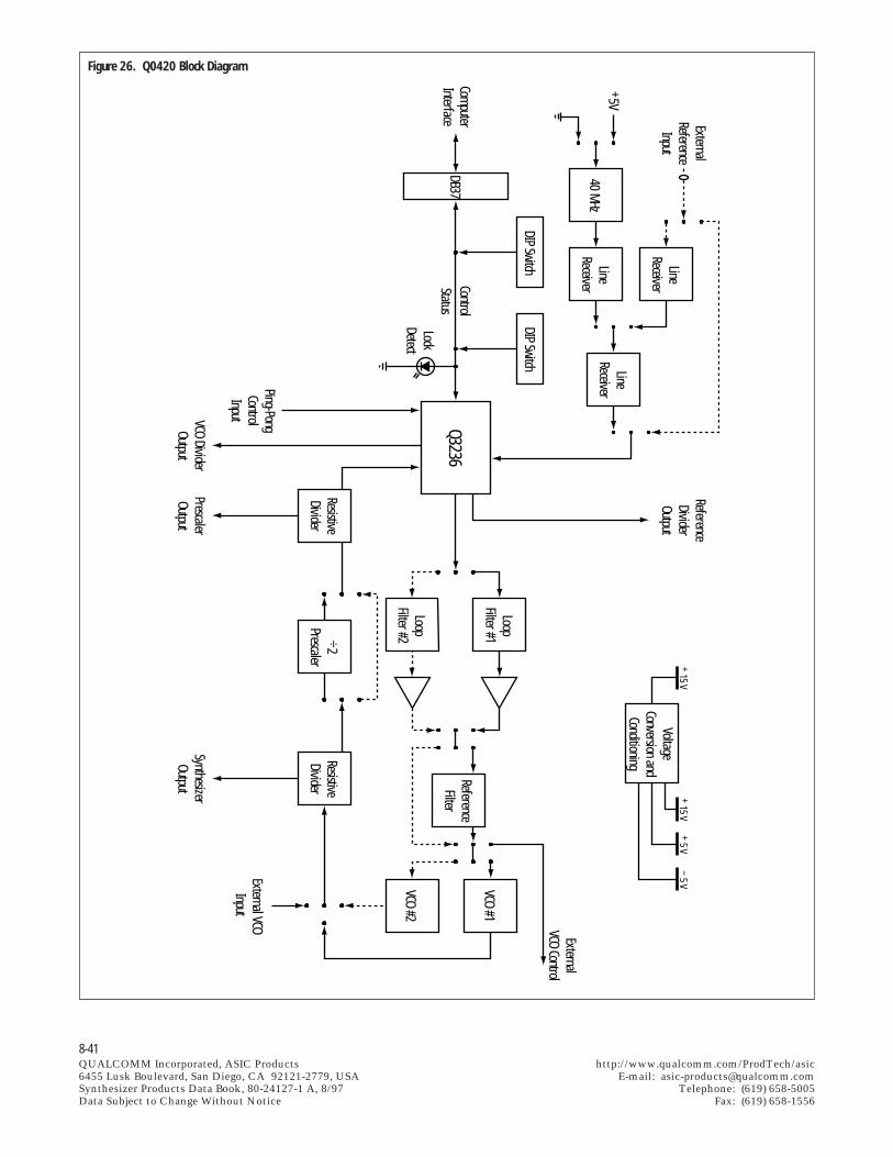
8-41QUALCOMM Incorporated, ASIC Products http://www.qualcomm.com/ProdTech/asic6455 Lusk Boulevard, San Diego, CA 92121-2779, USA E-mail: [email protected] Products Data Book, 80-24127-1 A, 8/97 Telephone: (619) 658-5005Data Subject to Change Without Notice Fax: (619) 658-1556
LineReceiver
LineReceiver
LoopFilter #1
ReferenceFilter
ResistiveDivider
VCO #1
VCO #2Loop
Filter #2
LineReceiver
40 MHz+5V
ExternalReference
Input
ComputerInterface
ReferenceDividerOutput
ExternalVCO Control
Q3236ControlStatus
LockDetect
DB37
DIP SwitchDIP Switch
External VCOInput
SynthesizerOutput
÷2Prescaler
ResistiveDivider
PrescalerOutput
Ping-PongControlInputVCO Divider
Output
VoltageConversion and
Conditioning
+ 15 V+ 15 V
+ 5 V– 5 V
Figure 26. Q0420 Block Diagram
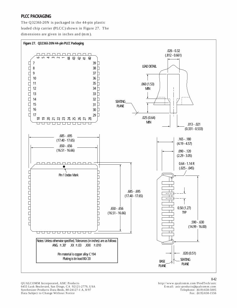
8-42QUALCOMM Incorporated, ASIC Products http://www.qualcomm.com/ProdTech/asic6455 Lusk Boulevard, San Diego, CA 92121-2779, USA E-mail: [email protected] Products Data Book, 80-24127-1 A, 8/97 Telephone: (619) 658-5005Data Subject to Change Without Notice Fax: (619) 658-1556
.685 - .695(17.40 - 17.65)
.685 - .695(17.40 - 17.65)
.650 - .656(16.51 - 16.66)
.650 - .656(16.51 - 16.66)
.165 - .180(4.19 - 4.57)
.090 - .120(2.29 - 3.05)
.020 (0.51)
BASEPLANE
SEATINGPLANE
SEATINGPLANE
0.64 - 1.14 R(.025 - .045)
LEAD DETAIL
.013 - .021(0.331 - 0.533)
.025 (0.64)MIN
.060 (1.53)MIN
.026 - 0.32(.812 - 0.661)
Pin 1 Index Mark
6 5 4 3 2 1 44 43 42 41 40
18 19 20 21 22 23 24 25 26 27 28
7891011121314151617
3938373635343332313029
.590 - .630(14.99 - 16.00)
0.50 (1.27)TYP
Notes: Unless otherwise specified, Tolerances (in inches) are as follows:ANG. ±.30' .XX ±.03 .XXX ±.010
Pin material is copper alloy C 194Plating is tin lead 80/20
PLCC PACKAGINGThe Q3236I-20N is packaged in the 44-pin plastic
leaded chip carrier (PLCC) shown in Figure 27. The
dimensions are given in inches and (mm).
Figure 27. Q3236I-20N 44-pin PLCC Packaging
8-43QUALCOMM Incorporated, ASIC Products http://www.qualcomm.com/ProdTech/asic6455 Lusk Boulevard, San Diego, CA 92121-2779, USA E-mail: [email protected] Products Data Book, 80-24127-1 A, 8/97 Telephone: (619) 658-5005Data Subject to Change Without Notice Fax: (619) 658-1556
RECOMMENDED SOCKETSWe recommend the low profile surface mount 44-pin
PLCC socket from Methode Electronic, Inc.
P/N 213-044-602. This socket is available from
QUALCOMM. Another recommended socket is the
AMP P/N 821575-1 thru-hole 44-pin carrier socket.
REFERENCES1.) F. M. Gardner, PhD, Phaselock Techniques, Second
Edition, John Wiley & Sons, Inc., New York, NY
1979
2.) V. Manassewitsch, Frequency Synthesizers , Theory
and Design, John Wiley & Sons, Inc., New York,
NY, 1987
3.) MECL Device Data, Motorola databook, 1989
4.) P. Gray, R. Paul, and R. Meyer, Analysis and
Design of Analog Integrated Circuits, Second
Edition, John Wiley & Sons, Inc., New York, NY,
1977, 1984
5.) Anatol I. Zverev, Handbook of Filter Synthesis ,
John Wiley & Sons, Inc., New York, NY , 1967
6.) Rohde, Ulrich L., Digital PLL Frequency
Synthesizers , Prentice-Hall, Inc., 1983
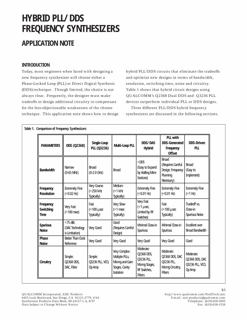
9-1QUALCOMM Incorporated, ASIC Products http://www.qualcomm.com/ProdTech/asic6455 Lusk Boulevard, San Diego, CA 92121-2779, USA E-mail: [email protected] Products Data Book, 80-24127-1 A, 8/97 Telephone: (619) 658-5005Data Subject to Change Without Notice Fax: (619) 658-1556
HYBRID PLL/DDSFREQUENCY SYNTHESIZERSAPPLICATION NOTE
hybrid PLL/DDS circuits that eliminate the tradeoffs
and optimize new designs in terms of bandwidth,
resolution, switching time, noise and circuitry.
Table 1 shows that hybrid circuit designs using
QUALCOMM’s Q2368 Dual DDS and Q3236 PLL
devices outperform individual PLL or DDS designs.
Three different PLL/DDS hybrid frequency
synthesizers are discussed in the following sections.
INTRODUCTIONToday, most engineers when faced with designing a
new frequency synthesizer will choose either a
Phase-Locked Loop (PLL) or Direct Digital Synthesis
(DDS) technique. Though limited, the choice is not
always clear. Frequently, the designer must make
tradeoffs or design additional circuitry to compensate
for the less-objectionable weaknesses of the chosen
technique. This application note shows how to design
PARAMETERS
Bandwidth
FrequencyResolution
FrequencySwitchingTime
SpuriousNoise
PhaseNoise
Circuitry
DDS (Q2368)
Narrow(0-65 MHz)
Extremely Fine(<0.02 Hz)
Very Fast(<100 nsec)
<75 dBc(DAC Technologyis Limitation)Better Than ClockReference
Simple:Q2368 DDS,DAC, Filter
Single-LoopPLL (Q3236)
Broad(0-2.0 GHz)
Very Course(>250 kHzTypically)
Fast(<100 µsecTypically)
Very Good
Very Good
Simple:Q3236 PLL, VCO,Op Amp
Multi-Loop PLL
Broad
Medium(>1 kHzTypically)
Very Slow(>1 msecTypically)
Good(Requires CarefulDesign)
Very Good
Very Complex:Multiple PLLs,Mixing and GainStages, CavityIsolation
DDS/DASHybrid
>DDS(Easy to Expandby Adding MoreSections)
Extremely Fine(<0.01 Hz)
Very Fast(<1 µsec,Limited by RFSwitches)
Minimal Close-in Spurious
Very Good
Moderate:Q2368 DDS,Q3236 PLL,Mixing Stages,RF Switches,Filters
PLL withDDS-Generated
FrequencyOffset
Broad(Requires CarefulDesign; FrequencyPlanningNecessary)
Extremely Fine(<0.01 Hz)
Fast(<100 µsecTypically)
Minimal Close-inSpurious
Very Good
Moderate:Q2368 DDS, DACQ3236 PLL,Mixing Circuitry,Filters
DDS-DrivenPLL
Broad(Easy toImplement)
Extremely Fine(<1 Hz)
Tradeoff vs.Close-inSpurious Noise
Excellent overBroad Bandwidth
Good
Moderate:Q2368 DDS, DACQ3236 PLL, VCO,Op Amp
Table 1. Comparison of Frequency Synthesizers
9-2QUALCOMM Incorporated, ASIC Products http://www.qualcomm.com/ProdTech/asic6455 Lusk Boulevard, San Diego, CA 92121-2779, USA E-mail: [email protected] Products Data Book, 80-24127-1 A, 8/97 Telephone: (619) 658-5005Data Subject to Change Without Notice Fax: (619) 658-1556
CONTENTSDDS/DAS HYBRID FREQUENCY SYNTHESIZER.................................................................................................... 9-3
Performance Advantages ...................................................................................................................................... 9-3
Design Advantages ............................................................................................................................................... 9-3
Circuit Analysis .................................................................................................................................................... 9-3
Performance Analysis ........................................................................................................................................... 9-3
PLL WITH DDS-GENERATED FREQUENCY OFFSET SYNTHESIZER.................................................................. 9-4
Performance Advantages ...................................................................................................................................... 9-4
Design Advantages ............................................................................................................................................... 9-4
Circuit Analysis .................................................................................................................................................... 9-4
Performance Analysis ........................................................................................................................................... 9-5
DDS-DRIVEN PLL FREQUENCY SYNTHESIZER ..................................................................................................... 9-5
Performance Advantages ...................................................................................................................................... 9-5
Design Advantages ............................................................................................................................................... 9-5
Circuit Analysis .................................................................................................................................................... 9-5
Performance Analysis ........................................................................................................................................... 9-6
ANALYSIS OF A PLL FREQUENCY MULTIPLIER WITH NOISY INPUT .............................................................. 9-6
Reference Frequency with AM Spurious Tones ................................................................................................. 9-6
Reference Frequency with PM Spurious Tones .................................................................................................. 9-6
Reference Frequency with FM Spurious Tones .................................................................................................. 9-7
Reference Frequency with Discrete Spurious Tones. ......................................................................................... 9-7
Reference Frequency with Phase Noise .............................................................................................................. 9-8
Reference Frequency with Additive White Noise .............................................................................................. 9-8
PERFORMANCE OF THE DDS-DRIVEN PLL............................................................................................................ 9-8
Spurs Due to Phase Truncation ........................................................................................................................... 9-8
Spurs Due to Amplitude Quantization ............................................................................................................... 9-8
Spurs Due to D/A Non-Linearities ...................................................................................................................... 9-8
Phase Noise ........................................................................................................................................................... 9-9
Additive Thermal Noise ...................................................................................................................................... 9-9
DDS-DRIVEN PLL DESIGN EXAMPLE .................................................................................................................... 9-10
REFERENCE ................................................................................................................................................................ 9-10
9-3QUALCOMM Incorporated, ASIC Products http://www.qualcomm.com/ProdTech/asic6455 Lusk Boulevard, San Diego, CA 92121-2779, USA E-mail: [email protected] Products Data Book, 80-24127-1 A, 8/97 Telephone: (619) 658-5005Data Subject to Change Without Notice Fax: (619) 658-1556
DDS/DAS HYBRID FREQUENCY SYNTHESIZERFigure 1 shows the Direct Digital Synthesizer (DDS)
/Direct Analog Synthesizer (DAS) hybrid frequency
synthesizer.
PERFORMANCE ADVANTAGES• Broad output bandwidth (the example below
shows 40 MHz from a 10 MHz DDS output).
• Extremely fine frequency resolution of <0.01 Hz
with a 42 MHz reference (the same as the DDS
chip).
• Fast settling time (the same as the DDS chip plus
the settling time of the RF switches).
• Fast switching speed (limited by the speed of the
RF switches).
• Multiple output ranges selected by RF switches.
The circuit shown below as an example has four
ranges:
• 187 – 197 MHz
• 197 – 207 MHz
• 207 – 217 MHz
• 217 – 227 MHz
The number of ranges is increased by adding more
local oscillator positions to each switch, and/or by
adding more mixing stages.
DDS 187-227MHz BPF
187-227 MHzD/A LPF
67-77 MHzBPF
77-87 MHzBPF
60 MHz 70 MHz 120 MHz 140 MHz
Q3236PLL
420 MHz
FrequencyReference
÷10
÷3
÷7
÷2
x2
60 MHz
140 MHz
70 MHz
120 MHz
42 MHzDDS Clock
DESIGN ADVANTAGES• No frequency multiplication
• To expand the bandwidth and increase the output
frequencies, just add more mixing stages, each
with two or more local oscillators.
CIRCUIT ANALYSISThe DDS/DAS hybrid synthesizer uses a phase-locked
loop to provide a fixed frequency clock for the DDS and
other fixed frequencies for mixing with the output of
the DDS.
PERFORMANCE ANALYSISPerformance analysis of the DDS/DAS hybrid
synthesizer is straightforward. Perform a conventional
intermodulation product analysis to determine the
spurious content of the output, then select the
frequency plan accordingly. Phase noise performance is
excellent due to the inherently high performance of the
DDS. Since the PLL is not required to switch between
output frequencies, optimization of its noise
performance is relatively easy.
Figure 1. Typical DDS/DAS Hybrid Frequency Synthesizer
9-4QUALCOMM Incorporated, ASIC Products http://www.qualcomm.com/ProdTech/asic6455 Lusk Boulevard, San Diego, CA 92121-2779, USA E-mail: [email protected] Products Data Book, 80-24127-1 A, 8/97 Telephone: (619) 658-5005Data Subject to Change Without Notice Fax: (619) 658-1556
PLL WITH DDS-GENERATED FREQUENCY OFFSETSYNTHESIZERFigure 2 shows a phase-locked loop synthesizer with
the internal offset frequency generated by a DDS.
PERFORMANCE ADVANTAGES• Broad output bandwidth (because the reference
frequency can be made relatively large).
• Extremely fine frequency resolution with
constant steps (because of the fine frequency
resolution of the DDS).
• Fast settling time (because of the wide loop
bandwidth made possible by the large reference
frequency).
• Low phase noise (because of the small loop
division ratio).
• Low spurious noise.
• Relatively low power.
DESIGN ADVANTAGES• Performance analysis is the same as a
conventional PLL synthesizer.
• Minimal circuitry.
CIRCUIT ANALYSISThe PLL with frequency offset approach is typical of
multi-loop synthesizer designs, but this hybrid replaces
Figure 2. PLL with DDS-Generated Frequency Offset
FREF
Q3236 PLL
Phase/FrequencyDetector
÷N
Loop Filter VCO
÷P
FOUT
OptionalDivider
OptionalUpconversion
Circuitry
BPF
BPF
Phase-LockedLocal
Oscillator
LPF D/A DDS
fine frequency step PLLs with a single DDS. Due to the
fine resolution of the DDS, this synthesizer can provide
better frequency resolution than a PLL approach
containing many loops. The local oscillator shown in
Figure 2 is optional; the DDS fundamental output can
be applied to the mixer directly. DDS image responses
may also be used, eliminating the need for the
upconverting LO.
If the design does not include the optional fixed
“÷ P” divider (P=1), then the synthesizer output
frequency is given by:
FOUT = N * FREF + FDDS + FLO (1)
The PLL provides the coarse steps in units of FREF. The
DDS provides the fine resolution to fill the gaps
between the coarse steps. For continuous frequency
coverage, the DDS output bandwidth must be greater
than or equal to the reference frequency:
BWDDS ≥ FREF (2)
The synthesizer step size is that of the DDS, usually
< 1 Hz.
If the design includes the optional fixed “÷ P” divider
between the synthesizer output and the mixer, then the
output frequency is given by:
FOUT = N * P * FREF + P * [FDDS + FLO] (3)
9-5QUALCOMM Incorporated, ASIC Products http://www.qualcomm.com/ProdTech/asic6455 Lusk Boulevard, San Diego, CA 92121-2779, USA E-mail: [email protected] Products Data Book, 80-24127-1 A, 8/97 Telephone: (619) 658-5005Data Subject to Change Without Notice Fax: (619) 658-1556
Figure 3. DDS-Driven PLL
As in the previous situation, the DDS bandwidth
BWDDS must be ≥ FREF. The frequency step size of this
synthesizer is as follows:
Step Size = (DDS Step Size) * P (4)
The DDS/PLL hybrid permits the reference
frequency to the PLL to be relatively large, while still
providing extremely fine frequency steps.
A large reference frequency provides three important
benefits:
1. The loop division ratio N is a low value. Since the
output phase noise within the loop bandwidth is
the reference phase noise + 20log(N) dB, a small
value of N minimizes this noise.
2. The loop bandwidth is typically ≤ 10% of the
reference frequency (this is a rule of thumb; a
detailed noise and stability analysis should be
performed for all PLL designs). Therefore, a large
reference frequency permits a wide loop bandwidth.
Since the VCO noise is suppressed by 12 dB/octave
beginning at ω 3dB and headed toward DC, a wide
loop bandwidth yields a low phase noise output
despite a noisy VCO.
3. The wide loop bandwidth made possible by this
synthesizer provides a loop with a proportionally
faster settling time.
PERFORMANCE ANALYSISSince this topology is similar to that of multi-loop
designs, the performance analysis is that of a
conventional PLL synthesizer. Of course, the DDS
provides its inherent benefits of fine frequency steps,
fast settling, and excellent phase noise and spurious
performance.
DDS-DRIVEN PLL FREQUENCY SYNTHESIZERFigure 3 shows a phase-locked loop frequency
synthesizer with the reference frequency generated by a
DDS.
PERFORMANCE ADVANTAGES• Broad output bandwidth.
• Fine frequency resolution (1 Hz or less).
• Fast switching time.
• Fast settling time.
• Low phase noise.
• Low spurious noise (the design uses no mixers).
• Relatively low power required.
DESIGN ADVANTAGES• Minimal circuitry required. A near octave-band
fine-resolution synthesizer with output greater
than 1500 MHz uses just four integrated circuits,
a band pass filter, and a VCO.
CIRCUIT ANALYSISA filtered, limited DDS output serves as the reference
for the PLL. An optional divider may be used to divide
the DDS output to provide an appropriate center
frequency for a particular filter technology (such as a
900 - 1600 MHz≈ 1 Hz Steps
50 MHzCrystal
9.5 MHz ± 100 kHz
94 ≤ N ≤ 169For This Application
Input Reference
Digital-to-
AnalogConverter
1/2QUALCOMM
Q2368Dual DDS
BandPassFilter
HardLimiter
ReferenceDivider
ModulusControl
VoltageControlledOscillator
Q3236 PLL
÷ 1Phase/
FrequencyDetector
LoopFilter
÷ A
÷ M ÷ 10/11
A 9.5 MHz ± 200 kHz BPFcan be added to
optimize spuriousperformance
9-6QUALCOMM Incorporated, ASIC Products http://www.qualcomm.com/ProdTech/asic6455 Lusk Boulevard, San Diego, CA 92121-2779, USA E-mail: [email protected] Products Data Book, 80-24127-1 A, 8/97 Telephone: (619) 658-5005Data Subject to Change Without Notice Fax: (619) 658-1556
crystal filter, where the range of center frequencies may
be limited), or simply to improve its noise and spurious
characteristics.
The DDS-driven PLL output frequency has the same
resolution as the input reference frequency. For
example, if the PLL output range is 200 to 400 MHz,
and if the reference frequency applied to the PLL is
10 MHz, the PLL can output 200, 210, 220, 230, ..., 390,
400 MHz. Each PLL output is the division ratio of the
loop (denoted as “N”) times the reference frequency.
Using a DDS as the loop reference lets the designer vary
the reference frequency in extremely small steps.
Appropriate selection of the DDS output bandwidth
gives the synthesizer continuous frequency coverage
with a resolution of N times the DDS frequency
resolution.
For continuous coverage, the DDS bandwidth must
be:
(5)
Where NMIN is the minimum PLL division ratio.
Note that the step size of the DDS-driven PLL varies
with N, and therefore is not constant throughout the
range of output frequencies.
PERFORMANCE ANALYSISIn the DDS-driven PLL, the DDS supplies the reference
frequency for the PLL. Ideally, the reference frequency
would have low phase noise and spurious content.
Although the DDS output does have low phase noise,
its spurious content exceeds that of a high-grade
reference oscillator. Therefore, performance analysis of
the DDS-driven PLL is divided into the following two
sections.
The first section, Analysis of a PLL Frequency
Multiplier with Noisy Input , shows how each of six
different types of frequency reference noise affects the
performance of a frequency multiplier PLL. The second
section, Performance of the DDS-driven PLL , analyzes
the performance as a function of the DDS
characteristics, the BPF bandwidth, and the PLL
parameters.
ANALYSIS OF A PLL FREQUENCY MULTIPLIER WITHNOISY INPUTA PLL with division ratio N acts as a frequency
multiplier for the signal applied to its reference input.
The loop acts as a first-order bandpass filter for the
multiplied signal; the one-sided bandwidth of the loop
equals the closed-loop bandwidth. The following noise
analysis is divided into six parts according to the type
of noise generated by the frequency reference:
• AM Spurious Tones
• PM Spurious Tones
• FM Spurious Tones
• Discrete Spurious Tones
• Phase Noise
• Additive White Noise
Each section first discusses the performance of an
xN frequency multiplier for the specific type of noisy
input, then superimposes the first-order response of the
PLL on the result of the noise analysis.
REFERENCE FREQUENCY WITH AM SPURIOUS TONESConsider an AM spectrum input to a frequency
multiplier:
x(t) = A (1 + m(t)) cos ω 1t (6)
If the frequency is multiplied by n = ω 2/ω 1,
the output of the frequency multiplier is:
y(t) = A(1 + m(t)) cos (nω 1t) (7)
The modulation index is not changed. The AM
spurs are no larger at the output of the multiplier than
at the input. In fact, AM spurs may be suppressed by a
limiter before or after frequency multiplication.
REFERENCE FREQUENCY WITH PM SPURIOUS TONESConsider a carrier phase modulated by a sinusoid:
y1(t) = A cos (ω 1t + β sin ω mt) (8)
Where β is the modulation index (β = maximum
value of the phase deviation). The phase of y1(t) is:
φ(y1(t)) = ω 1t + β sin ω mt (9)
BWDDS = DDS Center Frequency
NMIN
9-7QUALCOMM Incorporated, ASIC Products http://www.qualcomm.com/ProdTech/asic6455 Lusk Boulevard, San Diego, CA 92121-2779, USA E-mail: [email protected] Products Data Book, 80-24127-1 A, 8/97 Telephone: (619) 658-5005Data Subject to Change Without Notice Fax: (619) 658-1556
and the frequency is therefore
(10)
Multiplying this signal frequency by n = ω 2/ω 1
yields:
(11)
We integrate this to determine the phase:
φ (y1(t)) = ω 2t + n β sin ω mt (12)
Therefore,
y2(t) = A cos (ω 2t + n β sin ω mt) (13)
The modulation index is now nβ instead of β, but the
sideband offset frequency fm, which is equivalent to the
modulating frequency, is not changed.
The spectrum of the PM signal y1(t) is given by
inspection from the equivalent relationship:
(14)
Where Ji (β) are Bessel functions of the first kind.
Therefore, the spectrum of y2(t) is determined by
inspection from:
(15)
PM spurs centered about the carrier input to a
frequency multiplier are increased in amplitude only,
their offset from the carrier remains unchanged.
For sinusoidal modulation, frequency multiplication
by n increases the power of the PM spur at offset i* fm
from the carrier by the spur power ratio as follows:
(16)
Now consider the DDS-generated PM process where
the modulating waveform is a sawtooth of peak-to-peak
amplitude (2π/2P) radians. In this case, frequency
multiplication by n increases the amplitude of each
spurious tone by n, with no effect on the offset
frequency. Therefore, frequency multiplication by n
increases the power of DDS phase truncation spurs by
n2 (i.e. 20 log(n) dB), but does not change the frequency
offset of these spurs from the carrier.
REFERENCE FREQUENCY WITH FM SPURIOUS TONESConsider the FM modulated signal
Z1(t) = A cos (ω t + 2πfd ∫ t m(x)dx) (17)
where fd is the frequency deviation constant.
For m(t) = cos ω mt,
(18)
This is the identical analysis as for the PM case with
sinusoidal modulation. Note that for FM, unlike PM,
the modulation index is a function of the modulation
frequency. With this in mind, the same situation
occurs when an FM modulated signal is applied to a
frequency multiplier as with a PM modulated signal.
The modulation sidebands are increased in voltage as
Ji(nβ)/Ji(β); the frequency offset from the carrier is not
changed.
REFERENCE FREQUENCY WITH DISCRETE SPURIOUS TONES.This section discusses discrete spurs caused by
phenomena such as clock feedthrough, power supply
interference, stray coupling, harmonics of the reference
frequency, and intermodulation products between
reference frequency harmonics and other tones.
Symmetrical pairs of sidebands about the reference
may be AM or PM or a mixture of both. The phase
jitter contribution from a symmetrical pair of sidebands
is zero if they are AM. From Reference 1, the phase
jitter variance due to each pair of symmetrical PM
sidebands and the phase jitter variance from each single
discrete line (a line not part of a symmetrical pair) is
given by:
φ2 total = φ12 + φ2
2 + φ32 + …
This makes the conservative assumption that the
tones are PM in origin. The phase jitter due to discrete
additive spurious tones is increased n times at the
output of a xn frequency multiplier. The power of each
f1(t) =1
2πdφdt
=1
2π(ω1 + βωm cos ωmt)
f2(t) = n f1 (t) =
=
1
2π(nω1 + nβωm cos ωmt)
1
2π(ω2 + nβωm cos ωmt)
y1(t) = A cos (ω1t + β sin ωmt)
= A ΣJi (β) cos (ω1t + iωm)t∞
i = - ∞
y2(t) = A ΣJi (nβ) cos (ω2t + iωm)t∞
i = - ∞
spur power ratio = Ji (nβ)
Ji (β)
2
Z1(t) = A cos (ω1t +fd
fmsin ωmt)
9-8QUALCOMM Incorporated, ASIC Products http://www.qualcomm.com/ProdTech/asic6455 Lusk Boulevard, San Diego, CA 92121-2779, USA E-mail: [email protected] Products Data Book, 80-24127-1 A, 8/97 Telephone: (619) 658-5005Data Subject to Change Without Notice Fax: (619) 658-1556
spurious tone is increased by n2 (i.e. 20 log (n) dB).
Therefore, discrete spurious tones are increased in
power by n2 after frequency multiplication by n; their
offset from the reference frequency is not changed.
REFERENCE FREQUENCY WITH PHASE NOISEFrequency multiplication by n of a reference with phase
noise increases the phase noise power by
n2 (i.e. 20 log (n) dB).
REFERENCE FREQUENCY WITH ADDITIVE WHITE NOISEReference 1 analyzes in detail the effect frequency
multiplication has on additive SSB and DSB white
thermal noise. This section summarizes the results.
Superimposed SSB white Gaussian noise of noise
density N0 added to a clean carrier of power C can be
separated equally into an AM component and a PM
component. After frequency multiplication by n, the
modulation index of the PM component is multiplied
by n; the AM modulation index is not affected. For
n>>1, frequency multiplication turns additive SSB noise
into primarily DSB phase noise. Multiplying frequency
f1 by n to give frequency f2 yields the following carrier-
to-noise density ratio:
(19)
In the case of superimposed DSB white Gaussian
noise, the carrier-to-noise density ratios after frequency
multiplication by n are:
(20)
Therefore, frequency multiplication by n multiplies
phase noise power by n2 and additive DSB white
Gaussian noise by n2/2.
PERFORMANCE OF THE DDS-DRIVEN PLLHaving analyzed PLL noise performance, we can now
analyze the performance of the DDS-driven PLL shown
in Figure 3. The performance is a function of the DDS
characteristics, the BPF bandwidth, and the PLL
parameters.
If switching speed is unimportant, the PLL loop
bandwidth can be made extremely narrow. In this case,
the phase noise and spurious performance of the output
is essentially that of the VCO. The bandpass filter in
Figure 3 can be replaced with a lowpass filter since the
reference will have a minimal effect on the output
spectrum. If the VCO is clean, this may be the
simplest approach to a synthesizer with broad
bandwidth, fine resolution, good spurious and phase
noise performance, small size and low power, but with
slow switching between output frequencies.
For a fast switching speed, the PLL loop bandwidth
must be made correspondingly larger. In this case, the
bandpass filter and hard limiter in Figure 3, and an
optional divider become important. In the absence of
these functions, the unmodified DDS output (with anti-
aliasing filter) is multiplied by N in frequency by the
PLL. Within the loop bandwidth, noise and spurs are
affected as follows at the DDS output.
SPURS DUE TO PHASE TRUNCATIONThese spurs are multiplied in power by 20 log (N) dB;
their frequency offsets from the carrier are not changed.
They are filtered by 6 dB/octave by the PLL as a low
pass process from the closed loop bandwidth. Note that
DDS PM spurs are increased in power by precisely
20 log (N) dB, while a PM process with sinusoidal
modulation would be increased in amplitude by a ratio
of Bessel functions.
SPURS DUE TO AMPLITUDE QUANTIZATIONAs discussed previously, these tones are AM spurs.
Non-linearities may convert a portion of this process to
PM. Since frequency multiplication by N does not
change the modulation index of AM, the non-linear
PLL circuitry will tend to suppress the AM spurs. The
best thing to do is to hard limit the filtered DDS output
to suppress the AM spurs, or the AM component of the
noise process. The limiter is located prior to the PLL.
SPURS DUE TO D/A NON-LINEARITIESThese are additive discrete spurs, and therefore are
increased in power by 20 log (N) dB; their offsets from
the carrier are not changed. They are filtered by
6 dB/octave by the PLL low pass characteristic.
=Additive
SSB Noise
C
N0 2
4
n2
C
N0 1
= for n>>1
=Additive
DSB Noise
C
N0 2
2
n2
C
N0 1
=
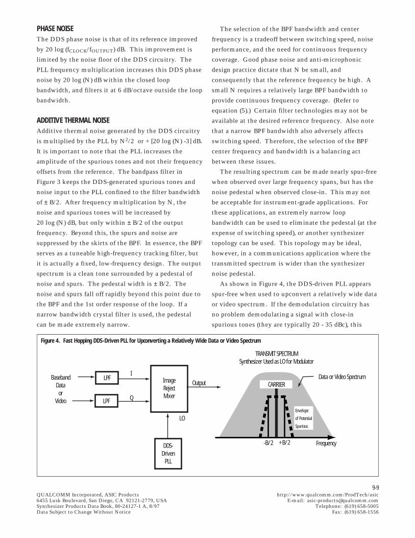
9-9QUALCOMM Incorporated, ASIC Products http://www.qualcomm.com/ProdTech/asic6455 Lusk Boulevard, San Diego, CA 92121-2779, USA E-mail: [email protected] Products Data Book, 80-24127-1 A, 8/97 Telephone: (619) 658-5005Data Subject to Change Without Notice Fax: (619) 658-1556
PHASE NOISEThe DDS phase noise is that of its reference improved
by 20 log (fCLOCK/fOUTPUT) dB. This improvement is
limited by the noise floor of the DDS circuitry. The
PLL frequency multiplication increases this DDS phase
noise by 20 log (N) dB within the closed loop
bandwidth, and filters it at 6 dB/octave outside the loop
bandwidth.
ADDITIVE THERMAL NOISEAdditive thermal noise generated by the DDS circuitry
is multiplied by the PLL by N2/2 or + [20 log (N) -3] dB.
It is important to note that the PLL increases the
amplitude of the spurious tones and not their frequency
offsets from the reference. The bandpass filter in
Figure 3 keeps the DDS-generated spurious tones and
noise input to the PLL confined to the filter bandwidth
of ± B/2. After frequency multiplication by N, the
noise and spurious tones will be increased by
20 log (N) dB, but only within ± B/2 of the output
frequency. Beyond this, the spurs and noise are
suppressed by the skirts of the BPF. In essence, the BPF
serves as a tuneable high-frequency tracking filter, but
it is actually a fixed, low-frequency design. The output
spectrum is a clean tone surrounded by a pedestal of
noise and spurs. The pedestal width is ± B/2. The
noise and spurs fall off rapidly beyond this point due to
the BPF and the 1st order response of the loop. If a
narrow bandwidth crystal filter is used, the pedestal
can be made extremely narrow.
The selection of the BPF bandwidth and center
frequency is a tradeoff between switching speed, noise
performance, and the need for continuous frequency
coverage. Good phase noise and anti-microphonic
design practice dictate that N be small, and
consequently that the reference frequency be high. A
small N requires a relatively large BPF bandwidth to
provide continuous frequency coverage. (Refer to
equation (5).) Certain filter technologies may not be
available at the desired reference frequency. Also note
that a narrow BPF bandwidth also adversely affects
switching speed. Therefore, the selection of the BPF
center frequency and bandwidth is a balancing act
between these issues.
The resulting spectrum can be made nearly spur-free
when observed over large frequency spans, but has the
noise pedestal when observed close-in. This may not
be acceptable for instrument-grade applications. For
these applications, an extremely narrow loop
bandwidth can be used to eliminate the pedestal (at the
expense of switching speed), or another synthesizer
topology can be used. This topology may be ideal,
however, in a communications application where the
transmitted spectrum is wider than the synthesizer
noise pedestal.
As shown in Figure 4, the DDS-driven PLL appears
spur-free when used to upconvert a relatively wide data
or video spectrum. If the demodulation circuitry has
no problem demodulating a signal with close-in
spurious tones (they are typically 20 - 35 dBc), this
Figure 4. Fast Hopping DDS-Driven PLL for Upconverting a Relatively Wide Data or Video Spectrum
Frequency
Data or Video Spectrum
-B/2 +B/2
Output
LO
BasebandDataor
Video
I
Q
CARRIER
TRANSMIT SPECTRUMSynthesizer Used as LO for Modulator
Envelope
of Potential
Spurious
LPF
LPF
ImageRejectMixer
DDS-Driven
PLL
9-10QUALCOMM Incorporated, ASIC Products http://www.qualcomm.com/ProdTech/asic6455 Lusk Boulevard, San Diego, CA 92121-2779, USA E-mail: [email protected] Products Data Book, 80-24127-1 A, 8/97 Telephone: (619) 658-5005Data Subject to Change Without Notice Fax: (619) 658-1556
synthesizer approach may be ideal.
The hard limiter in Figure 3 suppresses the AM
spurious components from the DDS. These
components are the AM amplitude quantization
process, as well as the AM portion of the DDS thermal
noise. As AM spurs have an unpredictable effect on
PLL output performance, it is best to eliminate them.
In practice, the hard limiter provides a noticeable
improvement in synthesizer performance.
An optional divider between the hard limiter and the
PLL’s input performs two functions. First, it improves
the spurious and noise performance of the DDS, in
general by 20 log(M) dB, where M = the divider value.
Second, it provides flexibility in selecting the reference
frequency to the PLL and the center frequency of the
crystal filter. This is because the DDS output and PLL
reference input are at different frequencies. The
resulting extra degree of freedom may help in the
specification of the BPF response.
DDS-DRIVEN PLL DESIGN EXAMPLEFigure 3 is a design example that uses the
QUALCOMM Q2368 Dual DDS and Q3236 PLL
integrated circuits. The following properties make this
combination ideal for use in the DDS-driven PLL:
1. The Q2368’s 32-bit frequency control provides
extremely fine tuning resolution to vary the
frequency step size at the synthesizer carrier
output.
2. The Q2368’s patented algorithmic sine lookup
function provides phase truncation spurs no larger
than -84 dBc (14 equivalent bits of phase).
3. The Q2368’s patented noise reduction circuit
provides excellent quantization performance using
an 8-bit D/A converter. Since the hard limiter
suppresses the AM component of quantization
noise, there may not be the need to use more than
an 8-bit D/A (given sufficient D/A linearity).
4. The Q2368 accepts a clock up to 130 MHz,
permitting the generation of high reference
frequencies.
5. The Q2368 Hop Clock input permits synchronous
frequency hopping.
6. The Q3236 can operate with an input reference and
phase comparison frequency up to 100 MHz
7. The Q3236 can operate up to 2.0 GHz with
feedback divide ratios as low as 20 and continuous
integer division starting at 90.
8. The Q3236’s direct parallel inputs can be hardwired
(no processor control required) for a fixed divide
ratio (÷N) when the synthesizer has narrow tuning
range requirements.
9. Since the Q3236 can operate with a high input
reference frequency, a very wide loop bandwidth
can be employed to facilitate fast frequency
switching at the expense of degrading the
synthesizer’s spurious output performance.
Figure 3 shows the block diagram of a synthesizer
that operates between 900 and 1600 MHz. The
frequency resolution is 2.0 Hz maximum. (It varies
between 1 Hz and 2 Hz across the band.) The DDS
output frequency is 9.5 MHz, and N in the PLL varies
between 94 and 169. The PLL loop bandwidth is
ω n ≈ 2 kHz.
The synthesizer has these resulting design
parameters:
• Maximum phase truncation spur within the BPF
and loop BW = -84 + 20log(169) dBc = -39 dBc.
• Amplitude quantization spurs suppressed by the
hard limiter.
• Maximum spurs due to the D/A non-linearities
within the BPF and loop BW ≈ -70 +20log(169) dBc
= -25 dBc.
Note: A careful choice of the DDS center
frequency can reduce this result.
REFERENCE1. Robins, W.P, Phase Noise in Signal Sources , Peter
Peregrinus Ltd., London, 1982.
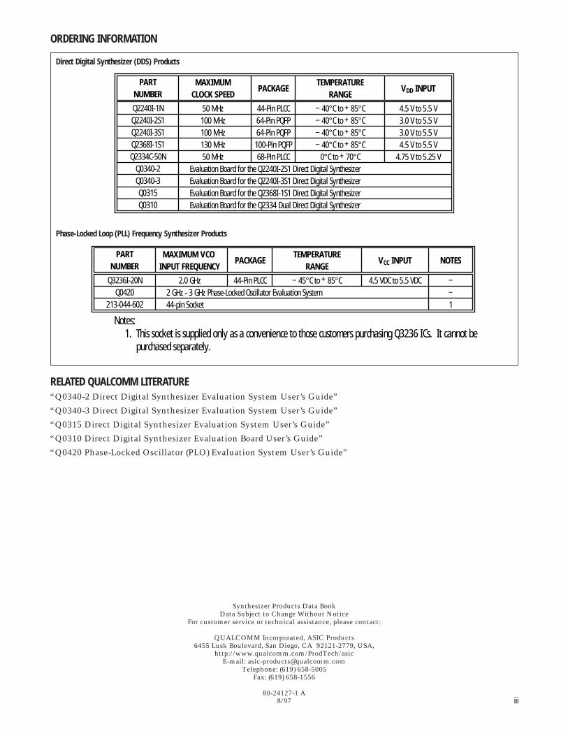
iii
ORDERING INFORMATION
TEMPERATURERANGE
– 40°C to + 85°C– 40°C to + 85°C– 40°C to + 85°C– 40°C to + 85°C
0°C to + 70°C
VDD INPUT
4.5 V to 5.5 V3.0 V to 5.5 V3.0 V to 5.5 V4.5 V to 5.5 V
4.75 V to 5.25 V
PACKAGE
44-Pin PLCC64-Pin PQFP64-Pin PQFP
100-Pin PQFP68-Pin PLCC
MAXIMUMCLOCK SPEED
50 MHz100 MHz100 MHz130 MHz50 MHz
Evaluation Board for the Q2240I-2S1 Direct Digital SynthesizerEvaluation Board for the Q2240I-3S1 Direct Digital SynthesizerEvaluation Board for the Q2368I-1S1 Direct Digital SynthesizerEvaluation Board for the Q2334 Dual Direct Digital Synthesizer
PARTNUMBER
Q2240I-1NQ2240I-2S1Q2240I-3S1Q2368I-1S1Q2334C-50N
Q0340-2Q0340-3Q0315Q0310
Direct Digital Synthesizer (DDS) Products
Phase-Locked Loop (PLL) Frequency Synthesizer Products
TEMPERATURERANGE
– 45°C to + 85°C
VCC INPUT
4.5 VDC to 5.5 VDC
NOTES
––1
PACKAGE
44-Pin PLCC
MAXIMUM VCO INPUT FREQUENCY
2.0 GHz2 GHz - 3 GHz Phase-Locked Oscillator Evaluation System44-pin Socket
PARTNUMBER
Q3236I-20NQ0420
213-044-602
Notes:1. This socket is supplied only as a convenience to those customers purchasing Q3236 ICs. It cannot be purchased separately.
RELATED QUALCOMM LITERATURE“Q0340-2 Direct Digital Synthesizer Evaluation System User’s Guide”
“Q0340-3 Direct Digital Synthesizer Evaluation System User’s Guide”
“Q0315 Direct Digital Synthesizer Evaluation System User’s Guide”
“Q0310 Direct Digital Synthesizer Evaluation Board User’s Guide”
“Q0420 Phase-Locked Oscillator (PLO) Evaluation System User’s Guide”
Synthesizer Products Data BookData Subject to Change Without Notice
For customer service or technical assistance, please contact:
QUALCOMM Incorporated, ASIC Products6455 Lusk Boulevard, San Diego, CA 92121-2779, USA,
http://www.qualcomm.com/ProdTech/asicE-mail: [email protected]
Telephone: (619) 658-5005Fax: (619) 658-1556
80-24127-1 A8/97

iv
Copyright © 1997 QUALCOMM Incorporated. All rights reserved.
Data subject to change.
U.S. Patent Nos. 4,901,265; 4,905,177; 4,926,130; 4,965,533; 5,028,887; 5,128,623