Embed Size (px)
Citation preview
1. Introduction
QN902x is an ultra low power, wireless System-on-Chip (SoC) for Bluetooth Smart applications. It supports both master and slave modes. QN902x integrates a high performance 2.4 GHz RF transceiver with a 32-bit ARM Cortex-M0 MCU, flash memory, and analog and digital peripherals.
By integrating a Bluetooth LE v4.2 compliant radio, link controller and host stack, QN902x provides a single-chip solution for Bluetooth Smart applications. The 32-bit ARM Cortex-M0 MCU and on-chip memory provides additional signal processing and room to run applications for a true single-chip Bluetooth Smart solution. In addition, QN902x can be used as a network processor by connecting to an application processor via UART or SPI. It helps to add Bluetooth Smart feature to any product.
QN902x has built-in analog and digital interfaces. It enables easy connection to any analog or digital peripheral, sensor, and external application processor in network processor mode.
2. General description
QN902x is an ultra low power, high performance and highly integrated Bluetooth LE solution. It is used in Bluetooth Smart applications such as sports and fitness, human interface devices, and app-enabled smart accessories. It is specially designed for wearable electronics and can run on a small capacity battery such as a coin cell battery.
QN902x integrates a Bluetooth LE radio, controller, protocol stack and profile software on a single chip, providing a flexible and easy to use Bluetooth LE SoC solution. It also has a high performance MCU and an on-chip memory that can support users to develop a single-chip wireless MCU solution. Users can also utilize QN902x as a network processor by connecting to an application processor for more advanced applications.
Additional system features include fully integrated DC-to-DC converter and LDO, low-power sleep timer, battery monitor, general-purpose ADC, and GPIOs. These features reduce overall system cost and size. QN902x has very low power consumption in all modes. It enables long life in battery-operated systems while maintaining excellent RF performance. QN9020/1 operates with a power supply range of 2.4 V to 3.6 V. The QN9022 operates with a power supply range of 1.8 V to 3.6 V.
3. Features and benefits
True single-chip Bluetooth LE SoC solution
Integrated Bluetooth LE radio
Complete Bluetooth LE protocol stack and application profiles
QN902xUltra low power Bluetooth LE system-on-chip solutionRev. 2.5 — 13 August 2018 Product data sheet

NXP Semiconductors QN902xUltra low power Bluetooth LE system-on-chip solution
Supports both master and slave modes
Supports secure connections
Up to eight simultaneous links in master mode
Frequency bands: 2400 MHz to 2483.5 MHz
1 Mbit/s on air data rate and 250 kHz deviation
GFSK modulation format
RF
95 dBm RX sensitivity (non-DC-to-DC mode)
93 dBm RX sensitivity (DC-to-DC mode)
TX output power from 20 dBm to +4 dBm
Fast and reliable RSSI and channel quality indication
Compatible with worldwide radio frequency regulations
Excellent link budget up to 99 dB
Very low power consumption
Single power supply of 2.4 V to 3.6 V for QN9020/1
Single power supply of 1.8 V to 3.6 V for QN9022
Integrated DC-to-DC converter and LDO
2 A deep sleep mode
3 A sleep mode (32 kHz RC oscillator on)
9.25 mA RX current with DC-to-DC converter
8.8 mA TX current @0 dBm TX power with DC-to-DC converter
Compact 6 mm 6 mm HVQFN48 package for QN9020, 5 mm 5 mm HVQFN32 package for QN9021, and 5 mm 5 mm HVQFN40 package for QN9022
Microcontroller
Integrated 32-bit ARM Cortex-M0 MCU
64 kB system memory
96 kB ROM
128 kB on-chip flash memory with 4 kB page size for QN9020 and QN9021 User-controllable code protection
High-level integration
4-channel, 10-bit general-purpose ADC
Two general-purpose analog comparators
31 GPIO pins for QN9020, 15 GPIO pins for QN9021, and 22 GPIO pins for QN9022
GPIO pins can be used as interrupt sources
Four general-purpose timers
32 kHz sleep timer
Watchdog timer
Real-time clock with calibration
2-channel programmable PWM
Two SPI/UART interfaces
I2C-bus master/slave interface
Brownout detector
Battery monitor
AES-128 security coprocessor
QN902x All information provided in this document is subject to legal disclaimers. © NXP Semiconductors N.V. 2018. All rights reserved.
Product data sheet Rev. 2.5 — 13 August 2018 2 of 44

NXP Semiconductors QN902xUltra low power Bluetooth LE system-on-chip solution
16 MHz or 32 MHz crystal oscillator
Low power 32 kHz RC oscillator
32.768 kHz crystal oscillator
4. Applications
Sports and fitness
Healthcare and medical
Remote control
Smartphone accessories
PC peripherals (mouse and keyboard)
Wireless sensor networks
5. Profiles and services
QN902x offers a complete list of qualified profiles and services.
Table 1. Supported profiles and services
Profiles and services Version
Device information service 1.1
Battery service 1.0
Blood pressure profile 1.0
Find me profile 1.0
Glucose profile 1.0
Heart rate profile 1.0
Health thermometer profile 1.0
HID over GATT profile 1.0
Proximity profile 1.0
Scan parameters profile 1.0
Time profile 1.0
Alert notification profile 1.0
Phone alert status profile 1.0
Cycling speed and cadence profile 1.0
Running speed and cadence profile 1.0
QN902x All information provided in this document is subject to legal disclaimers. © NXP Semiconductors N.V. 2018. All rights reserved.
Product data sheet Rev. 2.5 — 13 August 2018 3 of 44
NXP Semiconductors QN902xUltra low power Bluetooth LE system-on-chip solution
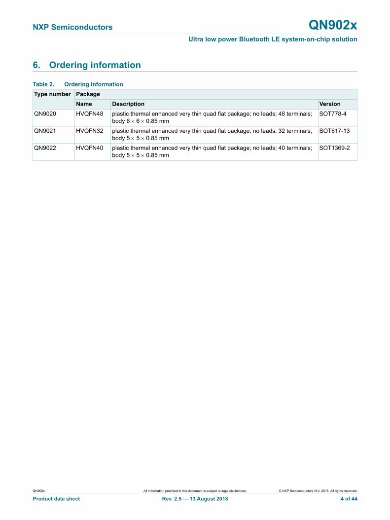
6. Ordering information
Table 2. Ordering information
Type number Package
Name Description Version
QN9020 HVQFN48 plastic thermal enhanced very thin quad flat package; no leads; 48 terminals; body 6 6 0.85 mm
SOT778-4
QN9021 HVQFN32 plastic thermal enhanced very thin quad flat package; no leads; 32 terminals; body 5 5 0.85 mm
SOT617-13
QN9022 HVQFN40 plastic thermal enhanced very thin quad flat package; no leads; 40 terminals; body 5 5 0.85 mm
SOT1369-2
QN902x All information provided in this document is subject to legal disclaimers. © NXP Semiconductors N.V. 2018. All rights reserved.
Product data sheet Rev. 2.5 — 13 August 2018 4 of 44

NXP Semiconductors QN902xUltra low power Bluetooth LE system-on-chip solution
7. Block diagram
Fig 1. Block diagram
QN902x All information provided in this document is subject to legal disclaimers. © NXP Semiconductors N.V. 2018. All rights reserved.
Product data sheet Rev. 2.5 — 13 August 2018 5 of 44
NXP Semiconductors QN902xUltra low power Bluetooth LE system-on-chip solution
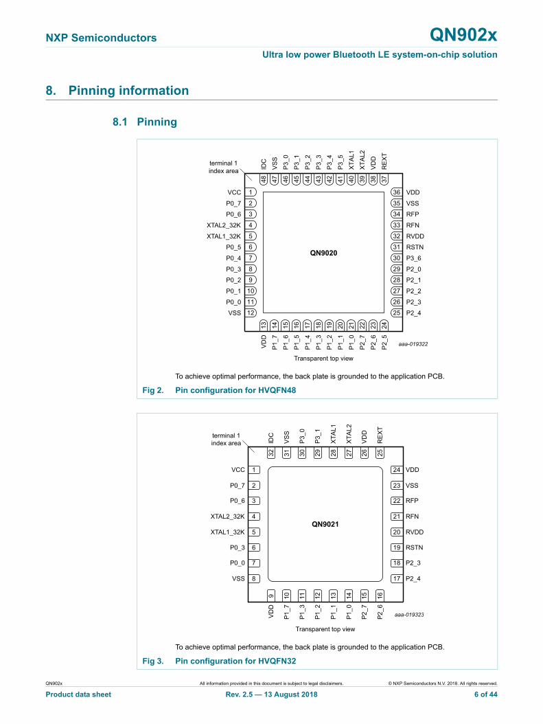
8. Pinning information
8.1 Pinning
To achieve optimal performance, the back plate is grounded to the application PCB.
Fig 2. Pin configuration for HVQFN48
To achieve optimal performance, the back plate is grounded to the application PCB.
Fig 3. Pin configuration for HVQFN32
QN902x All information provided in this document is subject to legal disclaimers. © NXP Semiconductors N.V. 2018. All rights reserved.
Product data sheet Rev. 2.5 — 13 August 2018 6 of 44

NXP Semiconductors QN902xUltra low power Bluetooth LE system-on-chip solution
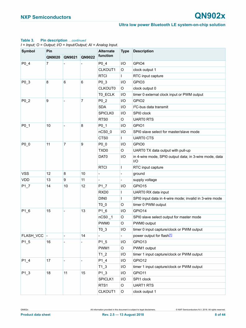
8.2 Pin description
To achieve optimal performance, the back plate is grounded to the application PCB.
Fig 4. Pin configuration for HVQFN40
Table 3. Pin descriptionI = Input; O = Output; I/O = Input/Output; AI = Analog Input.
Symbol Pin Alternate function
Type Description
QN9020 QN9021 QN9022
VCC 1 1 1 - - supply voltage
P0_7 2 2 2 SWCLK I default to SWCLK (input with pull-up)
P0_7 I/O GPIO7
AIN3 AI ADC input channel 3
ACMP1 AI analog comparator 1 negative input
P0_6 3 3 3 SWDIO I/O default to SWDIO (input with pull-up)
P0_6 I/O GPIO6
AIN2 AI ADC input channel 2
ACMP1+ AI analog comparator 1 positive input
XTAL2_32K 4 4 4 - - connected to 32.768 kHz crystal or external 32 kHz clock; if RC oscillator is used, this pin is not connected
XTAL1_32K 5 5 5 - - connected to 32.768 kHz crystal; if RC oscillator is used, this pin is not connected
P0_5 6 - - P0_5 I/O GPIO5
SCL I/O I2C-bus clock
ADCT I ADC conversion external trigger
ACMP1_O O analog comparator 1 output
QN902x All information provided in this document is subject to legal disclaimers. © NXP Semiconductors N.V. 2018. All rights reserved.
Product data sheet Rev. 2.5 — 13 August 2018 7 of 44
NXP Semiconductors QN902xUltra low power Bluetooth LE system-on-chip solution
P0_4 7 - - P0_4 I/O GPIO4
CLKOUT1 O clock output 1
RTCI I RTC input capture
P0_3 8 6 6 P0_3 I/O GPIO3
CLKOUT0 O clock output 0
T0_ECLK I/O timer 0 external clock input or PWM output
P0_2 9 - 7 P0_2 I/O GPIO2
SDA I/O I2C-bus data transmit
SPICLK0 I/O SPI0 clock
RTS0 O UART0 RTS
P0_1 10 - 8 P0_1 I/O GPIO1
nCS0_0 I/O SPI0 slave select for master/slave mode
CTS0 I UART0 CTS
P0_0 11 7 9 P0_0 I/O GPIO0
TXD0 O UART0 TX data output with pull-up
DAT0 I/O in 4-wire mode, SPI0 output data; in 3-wire mode, data I/O
RTCI I RTC input capture
VSS 12 8 10 - - ground
VDD 13 9 11 - - supply voltage
P1_7 14 10 12 P1_7 I/O GPIO15
RXD0 I UART0 RX data input
DIN0 I SPI0 input data in 4-wire mode; invalid in 3-wire mode
T0_0 O timer 0 PWM output
P1_6 15 - 13 P1_6 I/O GPIO14
nCS0 _1 O SPI0 slave select output for master mode
PWM0 O PWM0 output
T0_3 I/O timer 0 input capture/clock or PWM output
FLASH_VCC - - 14 - - power output for flash[1]
P1_5 16 - - P1_5 I/O GPIO13
PWM1 O PWM1 output
T1_2 I/O timer 1 input capture/clock or PWM output
P1_4 17 - - P1_4 I/O GPIO12
T1_3 I/O timer 1 input capture/clock or PWM output
P1_3 18 11 15 P1_3 I/O GPIO11
SPICLK1 I/O SPI1 clock
RTS1 O UART1 RTS
CLKOUT1 O clock output 1
Table 3. Pin description …continuedI = Input; O = Output; I/O = Input/Output; AI = Analog Input.
Symbol Pin Alternate function
Type Description
QN9020 QN9021 QN9022
QN902x All information provided in this document is subject to legal disclaimers. © NXP Semiconductors N.V. 2018. All rights reserved.
Product data sheet Rev. 2.5 — 13 August 2018 8 of 44

NXP Semiconductors QN902xUltra low power Bluetooth LE system-on-chip solution
P1_2 19 12 16 P1_2 I/O GPIO10
nCS1_0 I/O SPI1 slave select for master/slave mode
CTS1 I UART1 CTS
ADCT AI ADC conversion external trigger
P1_1 20 13 17 P1_1 I/O GPIO9
DAT1 I/O in 4-wire mode, SPI1 output data; in 3-wire mode, data I/O
TXD1 O UART1 TX data
T1_0 I/O timer 1 input capture/clock or PWM output
P1_0 21 14 18 P1_0 I/O GPIO8
DIN1 I SPI1 input data in 4-wire mode; invalid in 3-wire mode
RXD1 I UART1 RX data
T2_ECLK I/O timer 2 external clock input or PWM output
P2_7 22 15 19 P2_7 I/O GPIO23
ACMP1_O O analog comparator 1 output
PWM0 O PWM0 output
T1_ECLK I/O timer 1 external clock input or PWM output
P2_6 23 16 20 P2_6 I/O GPIO22
PWM1 O PWM1 output
T2_0 I/O timer 2 input capture/clock or PWM output
Fast Boot I Fast boot enable, pull low to bypass ISP function and start boot process directly
P2_5 24 - - P2_5 I/O GPIO21
nCS1_1 O SPI1 slave select output for master mode
T2_2 I/O timer 2 input capture/clock or PWM output
P2_4 25 17 21 P2_4 I/O GPIO20
SCL I/O I2C-bus master clock output with pull-up
PWM1 O PWM1 output
T3_ECLK I/O timer 3 external clock input or PWM output
P2_3 26 18 22 P2_3 I/O GPIO19
SDA I/O I2C-bus data transmit
ACMP0_O O analog comparator 0 output
T3_0 I/O timer 3 input capture/clock or PWM output
P2_2 27 - - P2_2 I/O GPIO18
SPICLK1 I/O SPI1 clock
RTS1 O UART1 RTS
T2_3 I/O timer 2 input capture/clock or PWM output
Table 3. Pin description …continuedI = Input; O = Output; I/O = Input/Output; AI = Analog Input.
Symbol Pin Alternate function
Type Description
QN9020 QN9021 QN9022
QN902x All information provided in this document is subject to legal disclaimers. © NXP Semiconductors N.V. 2018. All rights reserved.
Product data sheet Rev. 2.5 — 13 August 2018 9 of 44

NXP Semiconductors QN902xUltra low power Bluetooth LE system-on-chip solution
P2_1 28 - 23 P2_1 I/O GPIO17
DAT1 I/O in 4-wire mode, SPI0 output data; in 3-wire mode, data I/O
TXD1 O UART1 TX data output with pull-up
T3_1 I/O timer 3 input capture/clock or PWM output
P2_0 29 - 24 P2_0 I/O GPIO16
DIN1 I SPI1 input data in 4-wire mode; invalid in 3-wire mode
RXD1 I UART1 RX data input
T3_2 I/O timer 3 input capture/clock or PWM output
P3_6 30 - - P3_6 I/O GPIO30
nCS1_0 I/O SPI1 slave select for master/slave mode
CTS1 I UART1 CTS
RSTN 31 19 25 - - hardware reset, active LOW
RVDD 32 20 26 - - regulated PA power output
RFN 33 21 27 - - differential RF port
RFP 34 22 28 - - differential RF port
VSS 35 23 29 - - analog ground
VDD 36 24 30 - - analog power supply
REXT 37 25 31 - - current reference terminal, connect 56 k 1 % resistor to ground
VDD 38 26 32 - - analog power supply
XTAL2 39 27 33 - - connected to 16 MHz or 32 MHz crystal
XTAL1 40 28 34 - - connected to 16 MHz or 32 MHz crystal
P3_5 41 - - P3_5 I/O GPIO29
nCS0_0 I/O SPI0 slave select for master/slave mode
T0_0 I/O timer 0 input capture/clock or PWM output
P3_4 42 - - P3_4 I/O GPIO28
SPICLK0 I/O SPI0 clock
P3_3 43 - 35 P3_3 I/O GPIO27
DAT0 I/O in 4-wire mode, SPI0 output data; in 3-wire mode, data I/O
CLKOUT0 O clock output 0
P3_2 44 - 36 P3_2 I/O GPIO26
DIN0 I SPI0 input data in 4-wire mode; invalid in 3-wire mode
ACMP0_O O analog comparator 0 output
P3_1 45 29 37 P3_1 I/O GPIO25
T0_2 I/O timer 0 input capture/clock or PWM output
AIN1 I ADC input channel 1
ACMP0 I analog comparator 0 negative input
Table 3. Pin description …continuedI = Input; O = Output; I/O = Input/Output; AI = Analog Input.
Symbol Pin Alternate function
Type Description
QN9020 QN9021 QN9022
QN902x All information provided in this document is subject to legal disclaimers. © NXP Semiconductors N.V. 2018. All rights reserved.
Product data sheet Rev. 2.5 — 13 August 2018 10 of 44

NXP Semiconductors QN902xUltra low power Bluetooth LE system-on-chip solution
[1] Available only in QN9022.
9. Functional description
QN902x integrates an ultra low power 2.4 GHz radio, a qualified software stack and application profiles on a single chip. The integrated Power Management Unit (PMU) controls the system operation in different power states, to ensure low-power operation. The high-frequency crystal oscillator provides the reference frequency for the radio transceiver, while the low-frequency oscillators maintain timing in sleep states.
The integrated AES coprocessor supports encryption with minimal MCU usage. Minimum MCU usage helps in reducing the load on the MCU and also reduces power consumption. The embedded MCU and additional memory provides additional signal processing capability and helps to run user applications.
QN902x includes a general-purpose ADC with four external independent input channels. The ADC is utilized for power supply voltage monitoring. Digital serial interfaces (SPI/UART/I2C) are integrated to communicate with application processor or digital sensors.
The UART supports Bluetooth LE Direct Test Mode (DTM). This interface is used to control the PHY layer with commercially available Bluetooth testers, used for qualification.
I2C-bus is integrated and supports both master and slave mode. It can communicate with a digital sensor or EEPROM.
9.1 MCU subsystem
The MCU subsystem includes:
• 32-bit ARM Cortex-M0 MCU
• 64 kB system memory
• Reset generation
• Clock and power management unit
• Nested Vectored Interrupt Controller (NVIC)
• Serial Wire Debug (SWD) interface
P3_0 46 30 38 P3_0 I/O GPIO24
T2_1 I/O timer 1 input capture/clock or PWM output
AIN0 AI ADC input channel 0
ACMP0+ AI analog comparator 0 positive input
VSS 47 31 39 - - ground
IDC 48 32 40 - - if DC-to-DC is enabled, PWM driver is used for LC filter; if DC-to-DC is disabled, this pin is not connected
Table 3. Pin description …continuedI = Input; O = Output; I/O = Input/Output; AI = Analog Input.
Symbol Pin Alternate function
Type Description
QN9020 QN9021 QN9022
QN902x All information provided in this document is subject to legal disclaimers. © NXP Semiconductors N.V. 2018. All rights reserved.
Product data sheet Rev. 2.5 — 13 August 2018 11 of 44

NXP Semiconductors QN902xUltra low power Bluetooth LE system-on-chip solution
9.1.1 MCU
The CPU core is a 32-bit ARM Cortex-M0 MCU offering significant benefits to application development. It includes the following:
• Simple, easy-to-use programmers model
• Highly efficient ultra low power operation
• Excellent code density
• Deterministic, high-performance interrupt handling for 32 external interrupt inputs
The processor is extensively optimized for low power and delivers exceptional power efficiency through its efficient instruction set. It provides high-end processing hardware including a single-cycle multiplier.
9.1.2 Memory organization
QN902x has an on-chip system memory of 64 kB, used for storing application program and data. It is secured with a user-configurable protection mode, to prevent unauthorized access. The MCU is 32-bit, with an address space of 4 GB. It is shared between the system memory, ROM, system registers, peripheral registers, and general-purpose memory. The address space ranges from 0x0000 0000 to 0xFFFF FFFF; see Figure 5. The system memory is secured with a user-controllable protection scheme, which prevents unauthorized access.
9.1.3 RESET generation
The device has four sources of reset. The following events generate a reset:
• Forcing RSTN pin to LOW
Fig 5. Memory address map
QN902x All information provided in this document is subject to legal disclaimers. © NXP Semiconductors N.V. 2018. All rights reserved.
Product data sheet Rev. 2.5 — 13 August 2018 12 of 44
NXP Semiconductors QN902xUltra low power Bluetooth LE system-on-chip solution
• Power-on
• Brownout
• Watchdog time-out
9.1.4 Nested Vectored Interrupt Controller (NVIC)
QN902x supports Cortex-M0 built-in Nested Vectored Interrupt Controller (NVIC) with 24 external interrupt inputs. External interrupt signals are connected to the NVIC and the NVIC prioritizes the interrupts. Software is used to set the priority of each interrupt. The NVIC and Cortex-M0 processor core are closely coupled, providing low-latency interrupt processing and efficient processing of late arriving interrupts.
9.1.5 Clock and power management
QN902x provides flexible clocking scheme to balance between performance and power. A high frequency crystal oscillator is utilized to provide reference frequency and system clock. QN902x supports 16 MHz and 32 MHz external crystal with 50 106 accuracy. The system clock is 32 MHz or its divided versions.
Two low-speed 32 kHz oscillators are integrated. The 32.768 kHz crystal oscillator is used where accurate timing is needed, while a 32 kHz RC oscillator reduces cost and power consumption. Only one works at a time.
QN902x features ultra low power consumption with two sleep modes, SLEEP and DEEP SLEEP. After the execution of Wait For Interrupt (WFI) instruction, the MCU stops execution, enters into SLEEP mode and stops the clock immediately. Before entering into SLEEP mode, MCU should set the sleep timer correctly and make the 32 kHz clock ready. If DEEP SLEEP mode is entered, it must wait for the external interrupts to wake it up.
When an external interrupt or sleep timer time-out occurs, the Wake-up Interrupt Controller (WIC) enables the system clock. It takes 16 clock cycles to wake up the MCU and restore the states, before MCU can resume program execution to process the interrupt.
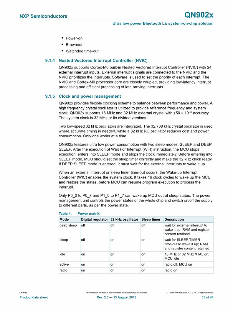
Only P0_0 to P0_7 and P1_0 to P1_7 can wake up MCU out of sleep states. The power management unit controls the power states of the whole chip and switch on/off the supply to different parts, as per the power state.
Table 4. Power matrix
Mode Digital regulator 32 kHz oscillator Sleep timer Description
deep sleep off off off wait for external interrupt to wake it up; RAM and register content retained
sleep off on on wait for SLEEP TIMER time-out to wake it up; RAM and register content retained
idle on on on 16 MHz or 32 MHz XTAL on; MCU idle
active on on on radio off; MCU on
radio on on on radio on
QN902x All information provided in this document is subject to legal disclaimers. © NXP Semiconductors N.V. 2018. All rights reserved.
Product data sheet Rev. 2.5 — 13 August 2018 13 of 44

NXP Semiconductors QN902xUltra low power Bluetooth LE system-on-chip solution
9.1.6 Serial Wire Debug (SWD) interface
QN902x provides a standard SWD interface and supports up to four hardware breakpoints and two watch points.
9.2 Flash
QN9020/1 have a 128 kB flash. The flash communicates with the MCU by internal SPI interface and can be used to store code or data. The flash has the following features:
• 32 equal sectors of 4 kB each, any sector can be erased individually
• Minimum 100000 erase/program cycles
• RES command, 1-byte command code
• Low power consumption
QN9022 has an interface to connect external flash.
9.3 Digital peripherals
9.3.1 TIMER 0/1/2/3
Timer 0 and timer 1 are general-purpose 32-bit timers whereas timer 2 and timer 3 are general-purpose 16-bit timers. Both have a programmable 10-bit prescaler. The prescaler source is a system clock, 32 kHz clock or an external clock input.
The timers have the following functions:
• Input capture function
• Compare function
• PWM output
The timers generate maskable interrupts in the event of overflow, compare and capture. They are used to trigger MCU or ADC conversions.
9.3.2 Real-Time Clock (RTC)
A 32 kHz clock runs the RTC, which provides real time with calibration. It supports the following functions:
• Time and date configuration on the fly
• One second interrupt generation, interrupt can be enabled or disabled through software
• Input capture function with programmable noise canceler
9.3.3 WatchDog Timer (WDT)
The WatchDog Timer (WDT) is a 16-bit timer clocked by a 32 kHz clock. It is used as a recovery method in situations where the CPU may be subjected to a software upset. The WDT resets the system when the software fails to clear the WDT within the selected time interval. The WDT is configured either as a watchdog timer or as an interval timer for general-purpose use. If WDT is configured as an interval timer, it can be used to generate interrupts at selected time intervals. The maximum time-out interval is 1.5 days.
QN902x All information provided in this document is subject to legal disclaimers. © NXP Semiconductors N.V. 2018. All rights reserved.
Product data sheet Rev. 2.5 — 13 August 2018 14 of 44
NXP Semiconductors QN902xUltra low power Bluetooth LE system-on-chip solution
9.3.4 Sleep timer
The sleep timer is a 32-bit timer running at 32 kHz clock rate. It is in always-on power domain, used to set the interval for system to exit sleep mode and wake up MCU.
9.3.5 PWM
The PWM provides two-channel PWM waveforms with programmable period and duty cycle. It has two 8-bit auto reload down counter and programmable 10-bit prescaler for both channels. It supports the functions mentioned below:
• Predictable PWM initial output state
• Buffered compare register and polarity register to ensure correct PWM output
• Programmable overflow interrupt generation
9.3.6 DMA
The DMA controller is used to relieve the MCU of handling data transfer operations, leading to high performance and efficiency. It has a single DMA channel to support fixed and undefined length transfer. The source address and the destination address are programmable. It can be aborted immediately in a transfer process by configuring ABORT register, and a DMA done interrupt is generated meanwhile.
9.3.7 Random number generator
QN902x integrates a random number generator for security purpose.
9.3.8 AES coprocessor
The Advanced Encryption Standard (AES) coprocessor allows encryption/decryption to be performed with minimal CPU usage. The coprocessor supports 128-bit key and DMA transfer trigger capability.
9.4 Communication interfaces
9.4.1 UART 0/1
UART 0 and UART 1 have identical functions and include the following features:
• 8-bit payload mode: 8-bit data without parity
• 9-bit payload mode: 8-bit data plus parity
• The parity in 9-bit mode is odd or even configurable
• Configurable start bit and stop bit levels
• Configurable LSB first or MSB first data transfer
• Parity and framing error status
• Configurable hardware flow control
• Support overrun
• Flexible baud rate: 1.2/2.4/4.8/9.6/14.4/19.2/28.8/38.4/57.6/76.8/115.2/230.4 kBd
9.4.2 SPI 0/1
SPI 0 and SPI 1 have identical functions and includes the following features:
QN902x All information provided in this document is subject to legal disclaimers. © NXP Semiconductors N.V. 2018. All rights reserved.
Product data sheet Rev. 2.5 — 13 August 2018 15 of 44

NXP Semiconductors QN902xUltra low power Bluetooth LE system-on-chip solution
• Master/slave mode configurable
• 4-wire or 3-wire configurable
• Clock speed configurable for master mode (divided from AHB clock)
• 4 MHz maximum clock speed in slave mode when AHB clock is 32 MHz
• 16 MHz maximum clock speed in master mode when AHB clock is 32 MHz
• Configurable clock polarity and phase
• Configurable LSB or MSB first transfer
9.4.3 I2C-bus
The I2C-bus module provides an interface between the device and I2C-bus compatible devices connected by a 2-wire serial I2C-bus. The I2C-bus module features include:
• Compliance with the I2C-bus specification v2.1
• 7-bit device addressing modes
• Standard mode up to 100 kbit/s and fast mode up to 400 kbit/s support
• Supports master arbitration in master mode
• Supports line stretch in slave mode
9.5 Radio and analog peripherals
9.5.1 RF transceiver
QN902x radio transceiver is compliant with volume 6, part A: physical layer specification for Bluetooth LE. The transceiver requires a 32 MHz or a 16 MHz crystal to provide reference frequency. It also requires a matching network to match an antenna connected to the receiver/transmitter pins.
9.5.2 On-chip oscillators
QN902x includes three integrated oscillators:
• HFXO: Low-power high frequency crystal oscillator supporting 32 MHz or 16 MHz external crystal
• LFXO: Ultra low power 32.768 kHz crystal oscillator
• LFRCO: Ultra low power 32 kHz RC oscillator with 250 106 frequency accuracy after calibration
The high frequency crystal oscillator (HFXO) provides the reference frequency for radio transceiver. The low frequency 32.768 kHz oscillators provide the protocol timing. The low-frequency clock can also be obtained from a 32.768 kHz external clock source. For HFXO, the external capacitance is integrated to reduce the BOM cost. Software is used to adjust the capacitance.
9.5.3 DC-to-DC converter
QN902x includes highly efficient integrated regulators to generate all the internal supply voltages from a single external supply voltage. Optional integrated DC-to-DC down-converter is used to reduce the current consumption by 30 %. It is useful for applications using battery technologies with higher nominal cell voltages.
QN902x All information provided in this document is subject to legal disclaimers. © NXP Semiconductors N.V. 2018. All rights reserved.
Product data sheet Rev. 2.5 — 13 August 2018 16 of 44

NXP Semiconductors QN902xUltra low power Bluetooth LE system-on-chip solution
9.5.4 General-purpose ADC
QN902x integrates a general-purpose 8-bit or 10-bit SAR ADC, with a sampling rate of up to 50 kilosample per second. It includes an analog multiplexer with up to four external input channels. Conversion results can be moved to memory through DMA.
The main features of the ADC are as follows:
• Four single-ended input channels, or two differential channels
• Reference voltage selectable as internal or external signal-ended
• Interrupt request generation
• DMA triggers at the end of conversions
• Window compare function
• Battery measurement capability
When using internal reference voltage, it is calibrated to achieve high resolution.
The ADC operates in the following three modes:
• Signal conversion mode
• Continuous conversion mode
• Scan mode (automatic switching among external inputs)
9.5.5 Analog comparator
The analog comparator is used to compare the voltage of two analog inputs and has a digital output to indicate the higher input voltage. The positive input is always from the external pin. The negative input can be either one of the selectable internal references or from an external pin.
The analog comparator features low-power operation. The comparison result is used as an interrupt source to wake up the system from SLEEP mode.
9.5.6 Battery monitor
A battery monitor is integrated by connecting supply voltage (VDD / 4) to the ADC input. It uses the internal regulated reference for conversion.
QN902x All information provided in this document is subject to legal disclaimers. © NXP Semiconductors N.V. 2018. All rights reserved.
Product data sheet Rev. 2.5 — 13 August 2018 17 of 44
NXP Semiconductors QN902xUltra low power Bluetooth LE system-on-chip solution
10. Limiting values
11. Recommended operating conditions
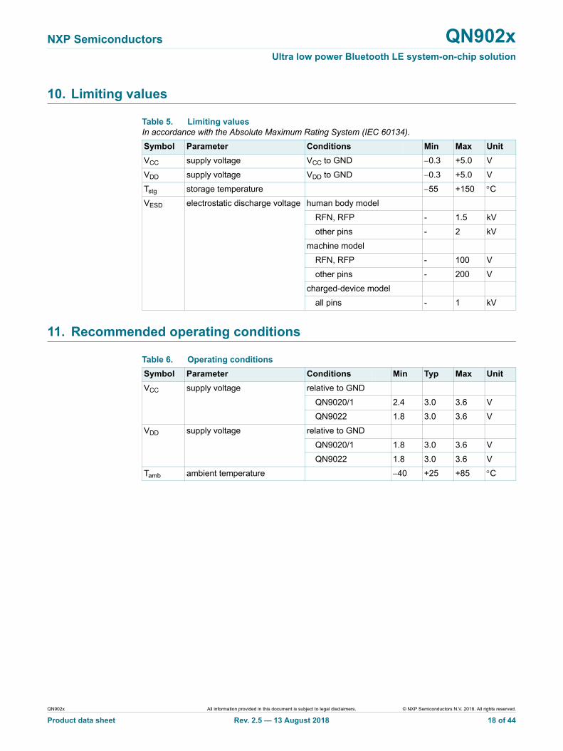
Table 5. Limiting valuesIn accordance with the Absolute Maximum Rating System (IEC 60134).
Symbol Parameter Conditions Min Max Unit
VCC supply voltage VCC to GND 0.3 +5.0 V
VDD supply voltage VDD to GND 0.3 +5.0 V
Tstg storage temperature 55 +150 C
VESD electrostatic discharge voltage human body model
RFN, RFP - 1.5 kV
other pins - 2 kV
machine model
RFN, RFP - 100 V
other pins - 200 V
charged-device model
all pins - 1 kV
Table 6. Operating conditions
Symbol Parameter Conditions Min Typ Max Unit
VCC supply voltage relative to GND
QN9020/1 2.4 3.0 3.6 V
QN9022 1.8 3.0 3.6 V
VDD supply voltage relative to GND
QN9020/1 1.8 3.0 3.6 V
QN9022 1.8 3.0 3.6 V
Tamb ambient temperature 40 +25 +85 C
QN902x All information provided in this document is subject to legal disclaimers. © NXP Semiconductors N.V. 2018. All rights reserved.
Product data sheet Rev. 2.5 — 13 August 2018 18 of 44

NXP Semiconductors QN902xUltra low power Bluetooth LE system-on-chip solution
12. Characteristics
12.1 DC characteristics
[1] Supply current for both analog and digital modes.
[2] Deep sleep mode: digital regulator off, no clocks, POR, RAM/register control retained.
[3] Sleep mode: digital regulator off, 32 kHz RC oscillator on, POR, sleep timer on, and RAM/register content retained.
[4] Idle: 16 MHz oscillator on, no radio or peripherals, 8 MHz system clock and MCU idle (no code execution).
[5] MCU@8 MHz: MCU running at 8 MHz RC oscillator, no radio peripherals.
[6] RX sensitivity is 95 dBm when DC-to-DC is disabled.
[7] RX sensitivity is 93 dBm when DC-to-DC is enabled.
[8] Depend on I/O conditions.
Table 7. DC characteristicsTypical values are Tamb = 25 C and VCC / VDD = 3 V.
Symbol Parameter Conditions Min Typ Max Unit
ICC supply current deep sleep mode [1][2] - 2 - A
sleep mode [1][3] - 3 - A
idle mode without DC-to-DC converter
[1][4] - 0.84 - mA
MCU @8 MHz without DC-to-DC converter
[1][5] - 1.35 - mA
RX mode without DC-to-DC converter
[1][6] - 13.6 - mA
RX mode with DC-to-DC converter [1][7] - 9.25 - mA
TX mode @0 dBm TX power without DC-to-DC converter
[1] 13.3 - mA
TX mode @0 dBm TX power with DC-to-DC converter
[1] - 8.8 - mA
tstartup start-up time RSTN pin remains at LOW level 50 - - s
Interface[8]
VOH HIGH-level output voltage
0.9 VCC - - V
VOL LOW-level output voltage
- - 0.1 VCC V
VIH HIGH-level input voltage
0.7 VCC - - V
VIL LOW-level input voltage
- - 0.3 VCC V
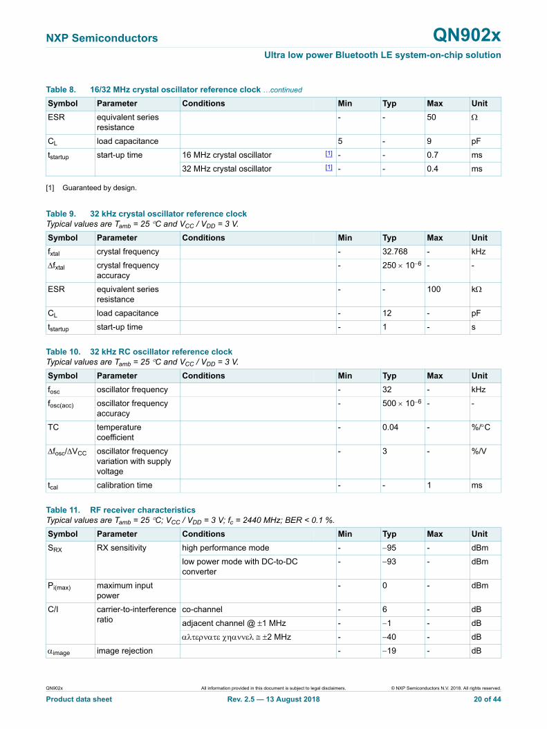
Table 8. 16/32 MHz crystal oscillator reference clock
Symbol Parameter Conditions Min Typ Max Unit
fxtal crystal frequency - 16 - MHz
- 32 - MHz
fxtal crystal frequency accuracy
50 106 - +50 106 -
QN902x All information provided in this document is subject to legal disclaimers. © NXP Semiconductors N.V. 2018. All rights reserved.
Product data sheet Rev. 2.5 — 13 August 2018 19 of 44
NXP Semiconductors QN902xUltra low power Bluetooth LE system-on-chip solution
[1] Guaranteed by design.
ESR equivalent series resistance
- - 50
CL load capacitance 5 - 9 pF
tstartup start-up time 16 MHz crystal oscillator [1] - - 0.7 ms
32 MHz crystal oscillator [1] - - 0.4 ms
Table 8. 16/32 MHz crystal oscillator reference clock …continued
Symbol Parameter Conditions Min Typ Max Unit
Table 9. 32 kHz crystal oscillator reference clockTypical values are Tamb = 25 C and VCC / VDD = 3 V.
Symbol Parameter Conditions Min Typ Max Unit
fxtal crystal frequency - 32.768 - kHz
fxtal crystal frequency accuracy
- 250 106 - -
ESR equivalent series resistance
- - 100 k
CL load capacitance - 12 - pF
tstartup start-up time - 1 - s
Table 10. 32 kHz RC oscillator reference clockTypical values are Tamb = 25 C and VCC / VDD = 3 V.
Symbol Parameter Conditions Min Typ Max Unit
fosc oscillator frequency - 32 - kHz
fosc(acc) oscillator frequency accuracy
- 500 106 - -
TC temperature coefficient
- 0.04 - %/C
fosc/VCC oscillator frequency variation with supply voltage
- 3 - %/V
tcal calibration time - - 1 ms
Table 11. RF receiver characteristicsTypical values are Tamb = 25 C; VCC / VDD = 3 V; fc = 2440 MHz; BER < 0.1 %.
Symbol Parameter Conditions Min Typ Max Unit
SRX RX sensitivity high performance mode - 95 - dBm
low power mode with DC-to-DC converter
- 93 - dBm
Pi(max) maximum input power
- 0 - dBm
C/I carrier-to-interference ratio
co-channel - 6 - dB
adjacent channel @ 1 MHz - 1 - dB
2 MHz - 40 - dB
image image rejection - 19 - dB
QN902x All information provided in this document is subject to legal disclaimers. © NXP Semiconductors N.V. 2018. All rights reserved.
Product data sheet Rev. 2.5 — 13 August 2018 20 of 44

NXP Semiconductors QN902xUltra low power Bluetooth LE system-on-chip solution
sup(oob) out-of-band suppression
30 MHz to 2000 MHz 18 - - dBm
2003 MHz to 2399 MHz 18 - - dBm
2484 MHz to 2997 MHz 18 - - dBm
3 GHz to 12.75 GHz 18 - - dBm
Table 11. RF receiver characteristics …continuedTypical values are Tamb = 25 C; VCC / VDD = 3 V; fc = 2440 MHz; BER < 0.1 %.
Symbol Parameter Conditions Min Typ Max Unit
Table 12. RF transmitter characteristicsTypical values are Tamb = 25 C; VCC / VDD = 3 V; fc = 2440 MHz.
Symbol Parameter Conditions Min Typ Max Unit
fo(RF) RF output frequency 2400 - 2483.5 MHz
CS channel separation - 2 - MHz
Po output power TX power without DC-to-DC converter
20 - +4 dBm
TX power with DC-to-DC converter 20 - +0.5 dBm
Po(RF)step RF output power step - 2 - dB
Po(acc) TX power accuracy 2 - +2 dB
ICC(TX) transmitter supply current
without DC-to-DC
4 dBm - 17.6 - mA
0 dBm - 13.3 - mA
4 dBm - 10.5 - mA
8 dBm - 8.3 - mA
20 dBm - 6.1 - mA
with DC-to-DC
0 dBm - 8.8 - mA
4 dBm - 6.9 - mA
8 dBm - 5.9 - mA
20 dBm - 4.3 - mA
Table 13. RSSI characteristicsTypical values are Tamb = 25 C and VCC / VDD = 3 V.
Symbol Parameter Conditions Min Typ Max Unit
RSSI(range) RSSI range 90 - 30 dBm
RSSI(acc) RSSI accuracy 4 - +4 dB
RSSI(res) RSSI resolution - 1 - dB
Table 14. ADC characteristicsTypical values are Tamb = 25 C and VCC / VDD = 3 V, with differential ADC input signal.
Symbol Parameter Conditions Min Typ Max Unit
VI(ADC) ADC input voltage single-ended mode 0 - Vref V
differential input mode Vref - +Vref V
ENOB effective number of bits
10-bit - 9.3 - bits
S/N signal-to-noise ratio 10-bit - 59.3 - dB
QN902x All information provided in this document is subject to legal disclaimers. © NXP Semiconductors N.V. 2018. All rights reserved.
Product data sheet Rev. 2.5 — 13 August 2018 21 of 44

NXP Semiconductors QN902xUltra low power Bluetooth LE system-on-chip solution
SFDR spurious-free dynamic range
10-bit - 65.2 - dB
THD total harmonic distortion
10-bit - 63 - dB
DNL differential non-linearity
10-bit 1 +0.6 +2 LSB
INL integral non-linearity 10-bit 2 +0.88 +3 LSB
tc(ADC) ADC conversion time 10-bit - 18 - s
EG gain error 10-bit - 4 10 LSB
EO offset error 10-bit - - 2 LSB
ICC(int)ADC ADC internal supply current
@1 MHz ADC clock
ADC - 50 65 A
buffer - 140 180 A
PGA - 90 120 A
Table 14. ADC characteristics …continuedTypical values are Tamb = 25 C and VCC / VDD = 3 V, with differential ADC input signal.
Symbol Parameter Conditions Min Typ Max Unit
Table 15. Battery monitor characteristicsTypical values are Tamb = 25 C and VCC / VDD = 3 V.
Symbol Parameter Conditions Min Typ Max Unit
Vmon(bat) battery monitor voltage
QN9020/1 2.4 - 3.6 V
QN9022 1.8 - 3.6 V
Vmon(bat)acc battery monitor accuracy
- 0.2 - mV
Table 16. Analog comparator characteristicsTypical values are Tamb = 25 C and VCC / VDD = 3 V.
Symbol Parameter Conditions Min Typ Max Unit
Vi input voltage 0 - VDD V
ICC(int)A analog internal supply current
- 0.3 - A
Vhys hysteresis - 40 - mV
QN902x All information provided in this document is subject to legal disclaimers. © NXP Semiconductors N.V. 2018. All rights reserved.
Product data sheet Rev. 2.5 — 13 August 2018 22 of 44
NXP Semiconductors QN902xUltra low power Bluetooth LE system-on-chip solution
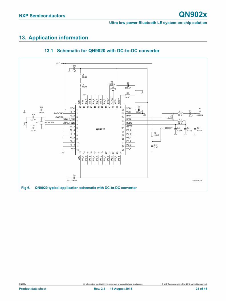
13. Application information
13.1 Schematic for QN9020 with DC-to-DC converter
Fig 6. QN9020 typical application schematic with DC-to-DC converter
QN902x All information provided in this document is subject to legal disclaimers. © NXP Semiconductors N.V. 2018. All rights reserved.
Product data sheet Rev. 2.5 — 13 August 2018 23 of 44

NXP Semiconductors QN902xUltra low power Bluetooth LE system-on-chip solution
13.2 Schematic for QN9020 without DC-to-DC converter
Fig 7. QN9020 typical application schematic without DC-to-DC converter
QN902x All information provided in this document is subject to legal disclaimers. © NXP Semiconductors N.V. 2018. All rights reserved.
Product data sheet Rev. 2.5 — 13 August 2018 24 of 44

NXP Semiconductors QN902xUltra low power Bluetooth LE system-on-chip solution
13.3 Schematic for QN9021 with DC-to-DC converter
Fig 8. QN9021 typical application schematic with DC-to-DC converter
QN902x All information provided in this document is subject to legal disclaimers. © NXP Semiconductors N.V. 2018. All rights reserved.
Product data sheet Rev. 2.5 — 13 August 2018 25 of 44

NXP Semiconductors QN902xUltra low power Bluetooth LE system-on-chip solution
13.4 Schematic for QN9021 without DC-to-DC converter
Fig 9. QN9021 typical application schematic without DC-to-DC converter
QN902x All information provided in this document is subject to legal disclaimers. © NXP Semiconductors N.V. 2018. All rights reserved.
Product data sheet Rev. 2.5 — 13 August 2018 26 of 44
NXP Semiconductors QN902xUltra low power Bluetooth LE system-on-chip solution
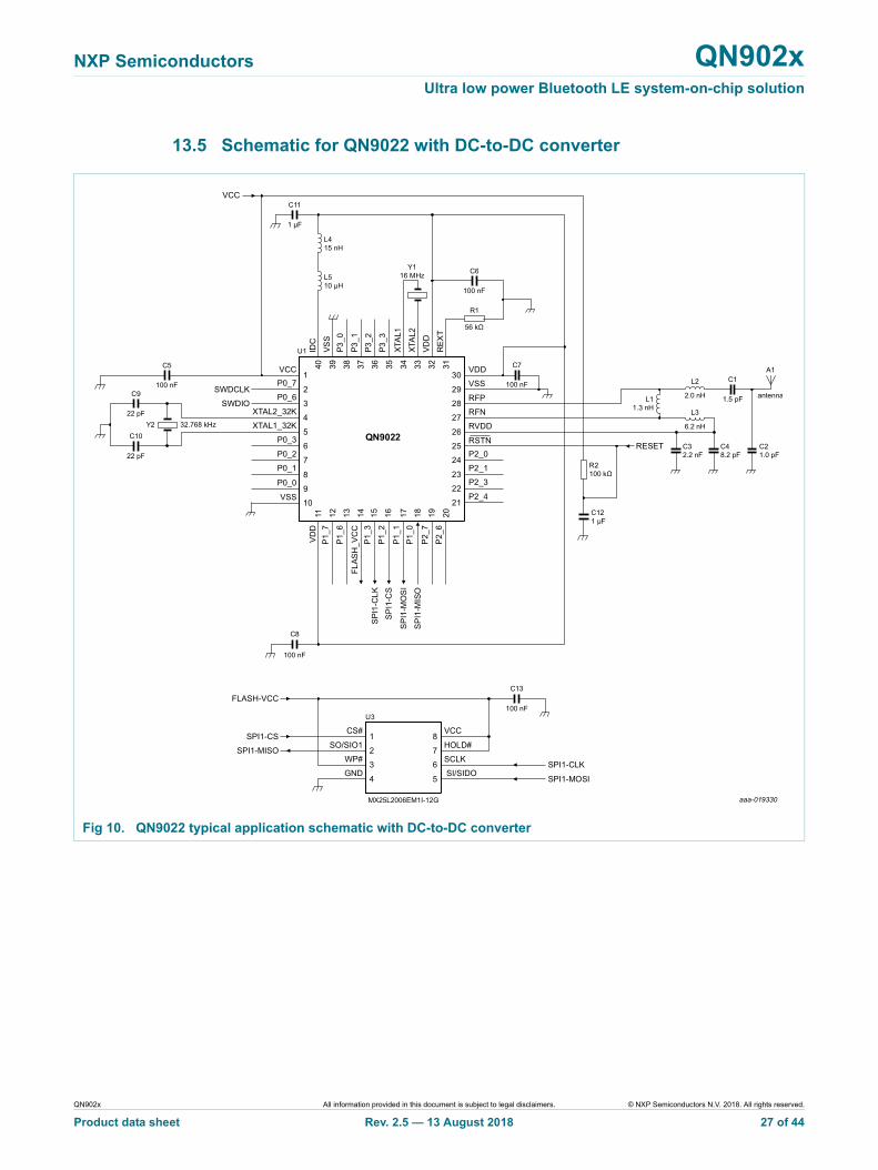
13.5 Schematic for QN9022 with DC-to-DC converter
Fig 10. QN9022 typical application schematic with DC-to-DC converter
QN902x All information provided in this document is subject to legal disclaimers. © NXP Semiconductors N.V. 2018. All rights reserved.
Product data sheet Rev. 2.5 — 13 August 2018 27 of 44

NXP Semiconductors QN902xUltra low power Bluetooth LE system-on-chip solution
13.6 Schematic for QN9022 without DC-to-DC converter
Fig 11. QN9022 typical application schematic without DC-to-DC converter
QN902x All information provided in this document is subject to legal disclaimers. © NXP Semiconductors N.V. 2018. All rights reserved.
Product data sheet Rev. 2.5 — 13 August 2018 28 of 44
NXP Semiconductors QN902xUltra low power Bluetooth LE system-on-chip solution
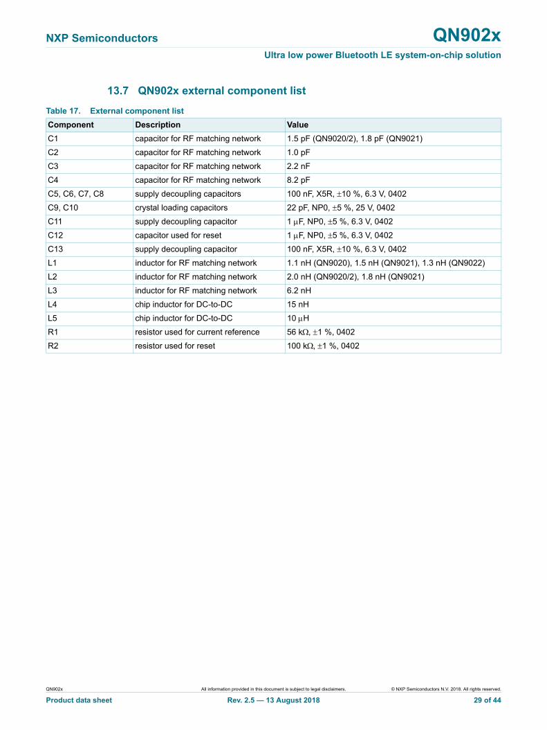
13.7 QN902x external component list
Table 17. External component list
Component Description Value
C1 capacitor for RF matching network 1.5 pF (QN9020/2), 1.8 pF (QN9021)
C2 capacitor for RF matching network 1.0 pF
C3 capacitor for RF matching network 2.2 nF
C4 capacitor for RF matching network 8.2 pF
C5, C6, C7, C8 supply decoupling capacitors 100 nF, X5R, 10 %, 6.3 V, 0402
C9, C10 crystal loading capacitors 22 pF, NP0, 5 %, 25 V, 0402
C11 supply decoupling capacitor 1 F, NP0, 5 %, 6.3 V, 0402
C12 capacitor used for reset 1 F, NP0, 5 %, 6.3 V, 0402
C13 supply decoupling capacitor 100 nF, X5R, 10 %, 6.3 V, 0402
L1 inductor for RF matching network 1.1 nH (QN9020), 1.5 nH (QN9021), 1.3 nH (QN9022)
L2 inductor for RF matching network 2.0 nH (QN9020/2), 1.8 nH (QN9021)
L3 inductor for RF matching network 6.2 nH
L4 chip inductor for DC-to-DC 15 nH
L5 chip inductor for DC-to-DC 10 H
R1 resistor used for current reference 56 k, 1 %, 0402
R2 resistor used for reset 100 k, 1 %, 0402
QN902x All information provided in this document is subject to legal disclaimers. © NXP Semiconductors N.V. 2018. All rights reserved.
Product data sheet Rev. 2.5 — 13 August 2018 29 of 44

NXP Semiconductors QN902xUltra low power Bluetooth LE system-on-chip solution
14. Package outline
Fig 12. Package outline SOT778-4 (HVQFN48)
QN902x All information provided in this document is subject to legal disclaimers. © NXP Semiconductors N.V. 2018. All rights reserved.
Product data sheet Rev. 2.5 — 13 August 2018 30 of 44

NXP Semiconductors QN902xUltra low power Bluetooth LE system-on-chip solution
Fig 13. Package outline SOT617-13 (HVQFN32)
QN902x All information provided in this document is subject to legal disclaimers. © NXP Semiconductors N.V. 2018. All rights reserved.
Product data sheet Rev. 2.5 — 13 August 2018 31 of 44

NXP Semiconductors QN902xUltra low power Bluetooth LE system-on-chip solution
Fig 14. Package outline SOT1369-2 (HVQFN40)
QN902x All information provided in this document is subject to legal disclaimers. © NXP Semiconductors N.V. 2018. All rights reserved.
Product data sheet Rev. 2.5 — 13 August 2018 32 of 44
NXP Semiconductors QN902xUltra low power Bluetooth LE system-on-chip solution
15. Soldering of SMD packages
This text provides a very brief insight into a complex technology. A more in-depth account of soldering ICs can be found in Application Note AN10365 “Surface mount reflow soldering description”.
15.1 Introduction to soldering
Soldering is one of the most common methods through which packages are attached to Printed Circuit Boards (PCBs), to form electrical circuits. The soldered joint provides both the mechanical and the electrical connection. There is no single soldering method that is ideal for all IC packages. Wave soldering is often preferred when through-hole and Surface Mount Devices (SMDs) are mixed on one printed wiring board; however, it is not suitable for fine pitch SMDs. Reflow soldering is ideal for the small pitches and high densities that come with increased miniaturization.
15.2 Wave and reflow soldering
Wave soldering is a joining technology in which the joints are made by solder coming from a standing wave of liquid solder. The wave soldering process is suitable for the following:
• Through-hole components
• Leaded or leadless SMDs, which are glued to the surface of the printed circuit board
Not all SMDs can be wave soldered. Packages with solder balls, and some leadless packages which have solder lands underneath the body, cannot be wave soldered. Also, leaded SMDs with leads having a pitch smaller than ~0.6 mm cannot be wave soldered, due to an increased probability of bridging.
The reflow soldering process involves applying solder paste to a board, followed by component placement and exposure to a temperature profile. Leaded packages, packages with solder balls, and leadless packages are all reflow solderable.
Key characteristics in both wave and reflow soldering are:
• Board specifications, including the board finish, solder masks and vias
• Package footprints, including solder thieves and orientation
• The moisture sensitivity level of the packages
• Package placement
• Inspection and repair
• Lead-free soldering versus SnPb soldering
15.3 Wave soldering
Key characteristics in wave soldering are:
• Process issues, such as application of adhesive and flux, clinching of leads, board transport, the solder wave parameters, and the time during which components are exposed to the wave
• Solder bath specifications, including temperature and impurities
QN902x All information provided in this document is subject to legal disclaimers. © NXP Semiconductors N.V. 2018. All rights reserved.
Product data sheet Rev. 2.5 — 13 August 2018 33 of 44
NXP Semiconductors QN902xUltra low power Bluetooth LE system-on-chip solution
15.4 Reflow soldering
Key characteristics in reflow soldering are:
• Lead-free versus SnPb soldering; note that a lead-free reflow process usually leads to higher minimum peak temperatures (see Figure 15) than a SnPb process, thus reducing the process window
• Solder paste printing issues including smearing, release, and adjusting the process window for a mix of large and small components on one board
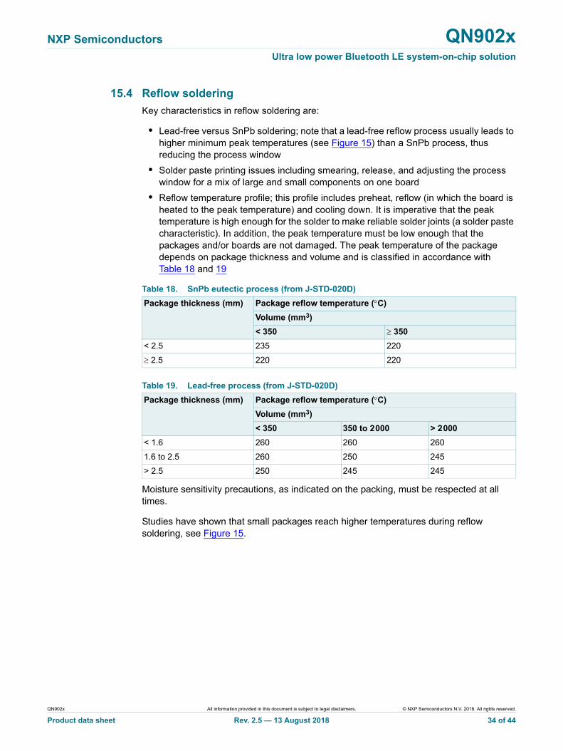
• Reflow temperature profile; this profile includes preheat, reflow (in which the board is heated to the peak temperature) and cooling down. It is imperative that the peak temperature is high enough for the solder to make reliable solder joints (a solder paste characteristic). In addition, the peak temperature must be low enough that the packages and/or boards are not damaged. The peak temperature of the package depends on package thickness and volume and is classified in accordance with Table 18 and 19
Moisture sensitivity precautions, as indicated on the packing, must be respected at all times.
Studies have shown that small packages reach higher temperatures during reflow soldering, see Figure 15.
Table 18. SnPb eutectic process (from J-STD-020D)
Package thickness (mm) Package reflow temperature (C)
Volume (mm3)
< 350 350
< 2.5 235 220
2.5 220 220
Table 19. Lead-free process (from J-STD-020D)
Package thickness (mm) Package reflow temperature (C)
Volume (mm3)
< 350 350 to 2000 > 2000
< 1.6 260 260 260
1.6 to 2.5 260 250 245
> 2.5 250 245 245
QN902x All information provided in this document is subject to legal disclaimers. © NXP Semiconductors N.V. 2018. All rights reserved.
Product data sheet Rev. 2.5 — 13 August 2018 34 of 44
NXP Semiconductors QN902xUltra low power Bluetooth LE system-on-chip solution
For further information on temperature profiles, refer to Application Note AN10365 “Surface mount reflow soldering description”.
MSL: Moisture Sensitivity Level
Fig 15. Temperature profiles for large and small components
001aac844
temperature
time
minimum peak temperature= minimum soldering temperature
maximum peak temperature= MSL limit, damage level
peak temperature
QN902x All information provided in this document is subject to legal disclaimers. © NXP Semiconductors N.V. 2018. All rights reserved.
Product data sheet Rev. 2.5 — 13 August 2018 35 of 44
NXP Semiconductors QN902xUltra low power Bluetooth LE system-on-chip solution
16. Abbreviations
Table 20. Abbreviations
Acronym Description
ADC Analog-to-Digital Converter
AES Advanced Encryption Standard
AHB AMBA High-performance Bus
BER Bit Error Rate
DTM Direct Test Mode
EEPROM Electrically Erasable Programmable Read Only Memory
GFSK Gaussian Frequency-Shift Keying
GPIO General Purpose Input Output
LDO Low DropOut
LE Low Energy
LSB Least Significant Bit
MCU MicroController Unit
MSB Most Significant Bit
PGA Programmable Gain Amplifier
PWM Pulse Width Modulation
RF Radio Frequency
RSSI Received Signal Strength Indicator
RTC Real-Time Clock
SAR Successive Approximation Register
S/N Signal-to-Noise ratio
SoC System-on-Chip
SPI Serial Peripheral Interface
SWD Serial Wire Debug
UART Universal Asynchronous Receiver Transmitter
QN902x All information provided in this document is subject to legal disclaimers. © NXP Semiconductors N.V. 2018. All rights reserved.
Product data sheet Rev. 2.5 — 13 August 2018 36 of 44
NXP Semiconductors QN902xUltra low power Bluetooth LE system-on-chip solution
17. Revision history
Table 21. Revision history
Document ID Release date Data sheet status Change notice Supersedes
QN902x v.2.5 20180418 Product data sheet
Modifications • Added alternate function Fast boot in Table 3 “Pin description” on page 6
QN902x v.2.4 20170116 Product data sheet - QN902x v.2.3
Modifications: • Minor update to VDD voltage for QN9020/1 Table 6 “Operating conditions” on page 17
QN902x v.2.3 20160905 Product data sheet - QN902x v.2.2
Modifications: • Minor update to XTAL1 and XTAL2 in Table 3 “Pin description” on page 6
QN902x v.2.2 20160825 Product data sheet - QN902x v.2.1
Modifications: • Minor update to Table 7 “DC characteristics” on page 18
QN902x v.2.1 20160414 Product data sheet - QN902x v.2
Modifications: • GPIO pin information and package details for QN9020/1/2 updated
• Update to Table 7
QN902x v.2 20160314 Product data sheet - QN902x v.1
Modifications: • Information about QN9022 is added to the data sheet
• Added RSSI characteristics Table 13
QN902x v.1 20150210 Product data sheet - -
QN902x All information provided in this document is subject to legal disclaimers. © NXP Semiconductors N.V. 2018. All rights reserved.
Product data sheet Rev. 2.5 — 13 August 2018 37 of 44
NXP Semiconductors QN902xUltra low power Bluetooth LE system-on-chip solution
18. Legal information
18.1 Data sheet status
[1] Please consult the most recently issued document before initiating or completing a design.
[2] The term ‘short data sheet’ is explained in section “Definitions”.
[3] The product status of device(s) described in this document may have changed since this document was published and may differ in case of multiple devices. The latest product status information is available on the Internet at URL http://www.nxp.com.
18.2 Definitions
Draft — The document is a draft version only. The content is still under internal review and subject to formal approval, which may result in modifications or additions. NXP Semiconductors does not give any representations or warranties as to the accuracy or completeness of information included herein and shall have no liability for the consequences of use of such information.
Short data sheet — A short data sheet is an extract from a full data sheet with the same product type number(s) and title. A short data sheet is intended for quick reference only and should not be relied upon to contain detailed and full information. For detailed and full information see the relevant full data sheet, which is available on request via the local NXP Semiconductors sales office. In case of any inconsistency or conflict with the short data sheet, the full data sheet shall prevail.
Product specification — The information and data provided in a Product data sheet shall define the specification of the product as agreed between NXP Semiconductors and its customer, unless NXP Semiconductors and customer have explicitly agreed otherwise in writing. In no event however, shall an agreement be valid in which the NXP Semiconductors product is deemed to offer functions and qualities beyond those described in the Product data sheet.
18.3 Disclaimers
Limited warranty and liability — Information in this document is believed to be accurate and reliable. However, NXP Semiconductors does not give any representations or warranties, expressed or implied, as to the accuracy or completeness of such information and shall have no liability for the consequences of use of such information. NXP Semiconductors takes no responsibility for the content in this document if provided by an information source outside of NXP Semiconductors.
In no event shall NXP Semiconductors be liable for any indirect, incidental, punitive, special or consequential damages (including - without limitation - lost profits, lost savings, business interruption, costs related to the removal or replacement of any products or rework charges) whether or not such damages are based on tort (including negligence), warranty, breach of contract or any other legal theory.
Notwithstanding any damages that customer might incur for any reason whatsoever, NXP Semiconductors’ aggregate and cumulative liability towards customer for the products described herein shall be limited in accordance with the Terms and conditions of commercial sale of NXP Semiconductors.
Right to make changes — NXP Semiconductors reserves the right to make changes to information published in this document, including without limitation specifications and product descriptions, at any time and without notice. This document supersedes and replaces all information supplied prior to the publication hereof.
Suitability for use — NXP Semiconductors products are not designed, authorized or warranted to be suitable for use in life support, life-critical or safety-critical systems or equipment, nor in applications where failure or malfunction of an NXP Semiconductors product can reasonably be expected to result in personal injury, death or severe property or environmental damage. NXP Semiconductors and its suppliers accept no liability for inclusion and/or use of NXP Semiconductors products in such equipment or applications and therefore such inclusion and/or use is at the customer’s own risk.
Applications — Applications that are described herein for any of these products are for illustrative purposes only. NXP Semiconductors makes no representation or warranty that such applications will be suitable for the specified use without further testing or modification.
Customers are responsible for the design and operation of their applications and products using NXP Semiconductors products, and NXP Semiconductors accepts no liability for any assistance with applications or customer product design. It is customer’s sole responsibility to determine whether the NXP Semiconductors product is suitable and fit for the customer’s applications and products planned, as well as for the planned application and use of customer’s third party customer(s). Customers should provide appropriate design and operating safeguards to minimize the risks associated with their applications and products.
NXP Semiconductors does not accept any liability related to any default, damage, costs or problem which is based on any weakness or default in the customer’s applications or products, or the application or use by customer’s third party customer(s). Customer is responsible for doing all necessary testing for the customer’s applications and products using NXP Semiconductors products in order to avoid a default of the applications and the products or of the application or use by customer’s third party customer(s). NXP does not accept any liability in this respect.
Limiting values — Stress above one or more limiting values (as defined in the Absolute Maximum Ratings System of IEC 60134) will cause permanent damage to the device. Limiting values are stress ratings only and (proper) operation of the device at these or any other conditions above those given in the Recommended operating conditions section (if present) or the Characteristics sections of this document is not warranted. Constant or repeated exposure to limiting values will permanently and irreversibly affect the quality and reliability of the device.
Terms and conditions of commercial sale — NXP Semiconductors products are sold subject to the general terms and conditions of commercial sale, as published at http://www.nxp.com/profile/terms, unless otherwise agreed in a valid written individual agreement. In case an individual agreement is concluded only the terms and conditions of the respective agreement shall apply. NXP Semiconductors hereby expressly objects to applying the customer’s general terms and conditions with regard to the purchase of NXP Semiconductors products by customer.
No offer to sell or license — Nothing in this document may be interpreted or construed as an offer to sell products that is open for acceptance or the grant, conveyance or implication of any license under any copyrights, patents or other industrial or intellectual property rights.
Document status[1][2] Product status[3] Definition
Objective [short] data sheet Development This document contains data from the objective specification for product development.
Preliminary [short] data sheet Qualification This document contains data from the preliminary specification.
Product [short] data sheet Production This document contains the product specification.
QN902x All information provided in this document is subject to legal disclaimers. © NXP Semiconductors N.V. 2018. All rights reserved.
Product data sheet Rev. 2.5 — 13 August 2018 38 of 44

NXP Semiconductors QN902xUltra low power Bluetooth LE system-on-chip solution
Export control — This document as well as the item(s) described herein may be subject to export control regulations. Export might require a prior authorization from competent authorities.
Non-automotive qualified products — Unless this data sheet expressly states that this specific NXP Semiconductors product is automotive qualified, the product is not suitable for automotive use. It is neither qualified nor tested in accordance with automotive testing or application requirements. NXP Semiconductors accepts no liability for inclusion and/or use of non-automotive qualified products in automotive equipment or applications.
In the event that customer uses the product for design-in and use in automotive applications to automotive specifications and standards, customer (a) shall use the product without NXP Semiconductors’ warranty of the product for such automotive applications, use and specifications, and (b)
whenever customer uses the product for automotive applications beyond NXP Semiconductors’ specifications such use shall be solely at customer’s own risk, and (c) customer fully indemnifies NXP Semiconductors for any liability, damages or failed product claims resulting from customer design and use of the product for automotive applications beyond NXP Semiconductors’ standard warranty and NXP Semiconductors’ product specifications.
18.4 TrademarksNotice: All referenced brands, product names, service names and trademarks are the property of their respective owners.
I2C-bus — logo is a trademark of NXP Semiconductors N.V.
19. Contact information
For more information, please visit: http://www.nxp.com
For sales office addresses, please send an email to: [email protected]
QN902x All information provided in this document is subject to legal disclaimers. © NXP Semiconductors N.V. 2018. All rights reserved.
Product data sheet Rev. 2.5 — 13 August 2018 39 of 44
NXP Semiconductors QN902xUltra low power Bluetooth LE system-on-chip solution
20. Tables
Table 1. Supported profiles and services . . . . . . . . . . . . .3Table 2. Ordering information. . . . . . . . . . . . . . . . . . . . . .3Table 3. Pin description . . . . . . . . . . . . . . . . . . . . . . . . . .6Table 4. Power matrix. . . . . . . . . . . . . . . . . . . . . . . . . . .12Table 5. Limiting values . . . . . . . . . . . . . . . . . . . . . . . . .17Table 6. Operating conditions. . . . . . . . . . . . . . . . . . . . .17Table 7. DC characteristics . . . . . . . . . . . . . . . . . . . . . .18Table 8. 16/32 MHz crystal oscillator reference clock . .18Table 9. 32 kHz crystal oscillator reference clock . . . . .19Table 10. 32 kHz RC oscillator reference clock . . . . . . . .19Table 11. RF receiver characteristics . . . . . . . . . . . . . . .19Table 12. RF transmitter characteristics . . . . . . . . . . . . . .20Table 13. RSSI characteristics . . . . . . . . . . . . . . . . . . . .20Table 14. ADC characteristics . . . . . . . . . . . . . . . . . . . . .20Table 15. Battery monitor characteristics . . . . . . . . . . . . .21Table 16. Analog comparator characteristics . . . . . . . . . .21Table 17. External component list . . . . . . . . . . . . . . . . . .28Table 18. SnPb eutectic process (from J-STD-020D) . . .33Table 19. Lead-free process (from J-STD-020D) . . . . . .33Table 20. Abbreviations . . . . . . . . . . . . . . . . . . . . . . . . . .35Table 21. Revision history . . . . . . . . . . . . . . . . . . . . . . . .36
QN902x All information provided in this document is subject to legal disclaimers. © NXP Semiconductors N.V. 2018. All rights reserved.
Product data sheet Rev. 2.5 — 13 August 2018 40 of 44
NXP Semiconductors QN902xUltra low power Bluetooth LE system-on-chip solution
21. Figures
Fig 1. Block diagram . . . . . . . . . . . . . . . . . . . . . . . . . . . .4Fig 2. Pin configuration for HVQFN48 . . . . . . . . . . . . . . .5Fig 3. Pin configuration for HVQFN32 . . . . . . . . . . . . . . .5Fig 4. Pin configuration for HVQFN40 . . . . . . . . . . . . . . .6Fig 5. Memory address map . . . . . . . . . . . . . . . . . . . . . 11Fig 6. QN9020 typical application schematic with
DC-to-DC converter . . . . . . . . . . . . . . . . . . . . . . .22Fig 7. QN9020 typical application schematic without
DC-to-DC converter . . . . . . . . . . . . . . . . . . . . . . .23Fig 8. QN9021 typical application schematic with
DC-to-DC converter . . . . . . . . . . . . . . . . . . . . . . .24Fig 9. QN9021 typical application schematic without
DC-to-DC converter . . . . . . . . . . . . . . . . . . . . . . .25Fig 10. QN9022 typical application schematic with
DC-to-DC converter . . . . . . . . . . . . . . . . . . . . . . .26Fig 11. QN9022 typical application schematic without
DC-to-DC converter . . . . . . . . . . . . . . . . . . . . . . .27Fig 12. Package outline SOT778-4 (HVQFN48) . . . . . . .29Fig 13. Package outline SOT617-13 (HVQFN32) . . . . . .30Fig 14. Package outline SOT1369-2 (HVQFN40) . . . . . .31Fig 15. Temperature profiles for large and small
components . . . . . . . . . . . . . . . . . . . . . . . . . . . . .34
© NXP Semiconductors N.V. 2018. All rights reserved.
For more information, please visit: http://www.nxp.comFor sales office addresses, please send an email to: [email protected]
Date of release: 13 August 2018
Document identifier: QN902x
Please be aware that important notices concerning this document and the product(s)described herein, have been included in section ‘Legal information’.

NXP Semiconductors QN902xUltra low power Bluetooth LE system-on-chip solution
22. Contents
1 Introduction . . . . . . . . . . . . . . . . . . . . . . . . . . . . 1
2 General description . . . . . . . . . . . . . . . . . . . . . . 1
3 Features and benefits . . . . . . . . . . . . . . . . . . . . 1
4 Applications . . . . . . . . . . . . . . . . . . . . . . . . . . . . 3
5 Profiles and services. . . . . . . . . . . . . . . . . . . . . 3
6 Ordering information. . . . . . . . . . . . . . . . . . . . . 3
7 Block diagram . . . . . . . . . . . . . . . . . . . . . . . . . . 4
8 Pinning information. . . . . . . . . . . . . . . . . . . . . . 58.1 Pinning . . . . . . . . . . . . . . . . . . . . . . . . . . . . . . . 58.2 Pin description . . . . . . . . . . . . . . . . . . . . . . . . . 6
9 Functional description . . . . . . . . . . . . . . . . . . 109.1 MCU subsystem . . . . . . . . . . . . . . . . . . . . . . . 109.1.1 MCU . . . . . . . . . . . . . . . . . . . . . . . . . . . . . . . . 119.1.2 Memory organization . . . . . . . . . . . . . . . . . . . 119.1.3 RESET generation . . . . . . . . . . . . . . . . . . . . . 119.1.4 Nested Vectored Interrupt Controller (NVIC) . 129.1.5 Clock and power management . . . . . . . . . . . . 129.1.6 Serial Wire Debug (SWD) interface . . . . . . . . 139.2 Flash. . . . . . . . . . . . . . . . . . . . . . . . . . . . . . . . 139.3 Digital peripherals . . . . . . . . . . . . . . . . . . . . . . 139.3.1 TIMER 0/1/2/3 . . . . . . . . . . . . . . . . . . . . . . . . 139.3.2 Real-Time Clock (RTC). . . . . . . . . . . . . . . . . . 139.3.3 WatchDog Timer (WDT) . . . . . . . . . . . . . . . . . 139.3.4 Sleep timer . . . . . . . . . . . . . . . . . . . . . . . . . . . 149.3.5 PWM. . . . . . . . . . . . . . . . . . . . . . . . . . . . . . . . 149.3.6 DMA . . . . . . . . . . . . . . . . . . . . . . . . . . . . . . . . 149.3.7 Random number generator . . . . . . . . . . . . . . 149.3.8 AES coprocessor . . . . . . . . . . . . . . . . . . . . . . 149.4 Communication interfaces . . . . . . . . . . . . . . . 149.4.1 UART 0/1 . . . . . . . . . . . . . . . . . . . . . . . . . . . . 149.4.2 SPI 0/1 . . . . . . . . . . . . . . . . . . . . . . . . . . . . . . 149.4.3 I2C-bus . . . . . . . . . . . . . . . . . . . . . . . . . . . . . . 159.5 Radio and analog peripherals. . . . . . . . . . . . . 159.5.1 RF transceiver . . . . . . . . . . . . . . . . . . . . . . . . 159.5.2 On-chip oscillators . . . . . . . . . . . . . . . . . . . . . 159.5.3 DC-to-DC converter . . . . . . . . . . . . . . . . . . . . 159.5.4 General-purpose ADC . . . . . . . . . . . . . . . . . . 169.5.5 Analog comparator . . . . . . . . . . . . . . . . . . . . . 169.5.6 Battery monitor . . . . . . . . . . . . . . . . . . . . . . . . 16
10 Limiting values. . . . . . . . . . . . . . . . . . . . . . . . . 17
11 Recommended operating conditions. . . . . . . 17
12 Characteristics. . . . . . . . . . . . . . . . . . . . . . . . . 1812.1 DC characteristics . . . . . . . . . . . . . . . . . . . . . 18
13 Application information. . . . . . . . . . . . . . . . . . 2213.1 Schematic for QN9020 with DC-to-DC
converter. . . . . . . . . . . . . . . . . . . . . . . . . . . . . 2213.2 Schematic for QN9020 without DC-to-DC converter 2313.3 Schematic for QN9021 with DC-to-DC
converter. . . . . . . . . . . . . . . . . . . . . . . . . . . . . 2413.4 Schematic for QN9021 without DC-to-DC converter 2513.5 Schematic for QN9022 with DC-to-DC
converter. . . . . . . . . . . . . . . . . . . . . . . . . . . . . 2613.6 Schematic for QN9022 without DC-to-DC converter 27
QN902x All information provided in this document is subject to legal disclaimers. © NXP Semiconductors N.V. 2018. All rights reserved.
Product data sheet Rev. 2.5 — 13 August 2018 42 of 44

NXP Semiconductors QN902xUltra low power Bluetooth LE system-on-chip solution
13.7 QN902x external component list . . . . . . . . . . 28
14 Package outline . . . . . . . . . . . . . . . . . . . . . . . . 29
15 Soldering of SMD packages . . . . . . . . . . . . . . 3215.1 Introduction to soldering . . . . . . . . . . . . . . . . . 3215.2 Wave and reflow soldering . . . . . . . . . . . . . . . 3215.3 Wave soldering . . . . . . . . . . . . . . . . . . . . . . . . 3215.4 Reflow soldering . . . . . . . . . . . . . . . . . . . . . . . 33
16 Abbreviations. . . . . . . . . . . . . . . . . . . . . . . . . . 35
17 Revision history. . . . . . . . . . . . . . . . . . . . . . . . 36
18 Legal information. . . . . . . . . . . . . . . . . . . . . . . 3718.1 Data sheet status . . . . . . . . . . . . . . . . . . . . . . 3718.2 Definitions. . . . . . . . . . . . . . . . . . . . . . . . . . . . 3718.3 Disclaimers . . . . . . . . . . . . . . . . . . . . . . . . . . . 3718.4 Trademarks. . . . . . . . . . . . . . . . . . . . . . . . . . . 38
19 Contact information. . . . . . . . . . . . . . . . . . . . . 38
20 Tables . . . . . . . . . . . . . . . . . . . . . . . . . . . . . . . . 39
21 Figures . . . . . . . . . . . . . . . . . . . . . . . . . . . . . . . 40
22 Contents . . . . . . . . . . . . . . . . . . . . . . . . . . . . . . 41
QN902x All information provided in this document is subject to legal disclaimers. © NXP Semiconductors N.V. 2018. All rights reserved.
Product data sheet Rev. 2.5 — 13 August 2018 43 of 44

NXP Semiconductors QN902xUltra low power Bluetooth LE system-on-chip solution
QN902x All information provided in this document is subject to legal disclaimers. © NXP Semiconductors N.V. 2018. All rights reserved.
Product data sheet Rev. 2.5 — 13 August 2018 44 of 44