Embed Size (px)
Citation preview

MAHARASHTRA STATE BOARD OF TECHNICAL EDUCATION (Autonomous)
(ISOIEC - 27001 - 2005 Certified)
SUMMER ndash 13 EXAMINATION Model Answer
Subject Code12269 Subject Name Embedded Systems
Page 1 of 46
Important Instructions to examiners 1) The answers should be examined by key words and not as word-to-word as given in the model answer scheme 2) The model answer and the answer written by candidate may vary but the examiner may try to assess the understanding level of the candidate 3) The language errors such as grammatical spelling errors should not be given more Importance (Not applicable for subject English and Communication Skills) 4) While assessing figures examiner may give credit for principl components indicated in the figure The figures drawn by candidate and model answer may vary The examiner may give credit for anyequivalent figure drawn 5) Credits may be given step wise for numerical problems In some cases the assumed constant values may vary and there may be some difference in the candidatersquos answers and model answer 6) In case of some questions credit may be given by judgement on part of examiner of relevant answer based on candidatersquos understanding 7) For programming language papers credit may be given to any other program based on equivalent
concept
Q1a) Attempt any THREE of the following MARKS 12
i) List ports available in 8051 microcontroller Give alternate function of port 3
( list of port- 1Mark Port3 functions- 3Marks)
i) port0 port1 port2 port3
PORT 3 ALTERNATE FUNCTION
MAHARASHTRA STATE BOARD OF TECHNICAL EDUCATION (Autonomous)
(ISOIEC - 27001 - 2005 Certified)
SUMMER ndash 13 EXAMINATION Model Answer
Subject Code12269 Subject Name Embedded Systems
Page 2 of 46
ii) State the types of serial protocol Describe any one in brief
(Types 1-Mark any one explanation for given type 3-Marks)
There are 4 most popular serial protocols
1 I2C Bus (Inter integrated circuit Communication)
2 CAN (Controller area net network) bys
3 Fire Wire
4 USB (Universal serial bus)
I2C Bus
Integrated Circuit 1 Integrated Circuit 2
SDA
SCL
It is designed by Philips It is two bus interface and has two communication lines called serial
data line (SDA) serial clock line (SCL) Each devices has unique address and master slave
relationship between the device on the bus The data transmission is in multiple of 8 Bits There
are 3 modes standard look bitSec hookbitSec high speed 34 M bitSec It generates clock signal
(SCL) to starts with START condition amp ends with Stop condition The 9 clock pulses are required
to transmit each bye
SCL
Bit 7 Bit 6 Bit 5 Bit 4 Bit 3 Bit 2 Bit 1 Bit 0 Ack Bit
Pressure System Temperature System
Controller Level Sensing System
MAHARASHTRA STATE BOARD OF TECHNICAL EDUCATION (Autonomous)
(ISOIEC - 27001 - 2005 Certified)
SUMMER ndash 13 EXAMINATION Model Answer
Subject Code12269 Subject Name Embedded Systems
Page 3 of 46
SDA
Transmitter _________
Receiver ----------
bull CAN (Controller Area Network)
ndash Protocol for real-time applications
ndash Developed by Robert Bosch GmbH
ndash Originally for communication among components of cars
ndash Applications now using CAN include
bull elevator controllers copiers telescopes production-line control systems and
medical instruments
ndash Data transfer rates up to 1 Mbits and 11-bit addressing
ndash Common devices interfacing with CAN
bull 8051-compatible 8592 processor and standalone CAN controllers
ndash Actual physical design of CAN bus not specified in protocol
bull Requires devices to transmitdetect dominant and recessive signals tofrom bus
bull eg bdquo1‟ = dominant bdquo0‟ = recessive if single data wire used
bull Bus guarantees dominant signal prevails over recessive signal if asserted
simultaneously
bull FireWire
ndash High-performance serial bus developed by Apple Computer Inc
ndash Designed for interfacing independent electronic components
bull eg Desktop scanner
ndash Data transfer rates from 125 to 400 Mbitss 64-bit addressing
ndash Plug-and-play capabilities
ndash Packet-based layered design structure
ndash Applications using FireWire include
bull disk drives printers scanners cameras
MAHARASHTRA STATE BOARD OF TECHNICAL EDUCATION (Autonomous)
(ISOIEC - 27001 - 2005 Certified)
SUMMER ndash 13 EXAMINATION Model Answer
Subject Code12269 Subject Name Embedded Systems
Page 4 of 46
ndash Capable of supporting a LAN similar to Ethernet
bull 64-bit address
bull 10 bits for network ids 1023 subnetworks
bull 6 bits for node ids each subnetwork can have 63 nodes
bull 48 bits for memory address each node can have 281 terabytes of distinct
locations
bull USB (Universal Serial Bus)
ndash Easier connection between PC and monitors printers digital speakers modems scanners
digital cameras joysticks multimedia game equipment
ndash 2 data rates
bull 12 Mbps for increased bandwidth devices
bull 15 Mbps for lower-speed devices (joysticks game pads)
ndash Tiered star topology can be used
bull One USB device (hub) connected to PC
bull hub can be embedded in devices like monitor printer or keyboard or can be
standalone
bull Multiple USB devices can be connected to hub
bull Up to 127 devices can be connected like this
ndash USB host controller
bull Manages and controls bandwidth and driver software required by each peripheral
bull Dynamically allocates power downstream according to devices
connecteddisconnected
MAHARASHTRA STATE BOARD OF TECHNICAL EDUCATION (Autonomous)
(ISOIEC - 27001 - 2005 Certified)
SUMMER ndash 13 EXAMINATION Model Answer
Subject Code12269 Subject Name Embedded Systems
Page 5 of 46
iii) Describe in brief use of simulator and emulator in embedded system design and testing
(Simulator 2-Marks Emulator-2-Marks)
Simulator A simulator is software tool that runs on the host and simulates the behavior of the
target‟s processor and memory The simulator knows the target processor‟s architecture and
instruction set The program to be tested is read by the simulator and as instructions are executed
the simulator keeps track of the values of the target processor‟s registers and the target‟s memory
Simulators provide single step and breakpoint facilities to debug the program Simulators cannot
be used if the embedded system uses special hardware that cannot be simulated and the only way
to test the program is to execute it on the target Although simulators do not run at the same speed
as the target microprocessor they provide details from which the time taken to execute the code on
the target microprocessor can be determined For instance the simulator can report the number of
target microprocessor‟s bus cycles taken to execute the code Multiplying this value with the time
taken for one bus cycle gives the actual time taken by the target microprocessor to execute the
code
Emulator An emulator is a hardware tool that helps in testing and debugging the program on the
target The target‟s processor is removed from the circuit and the emulator is connected in its
place The emulator drives the signals in the circuit in the same way as the target‟s processor and
hence the emulator appears to be the processor to all other components of the embedded system
Emulators also provide features such as single step and breakpoints to debug the program
MAHARASHTRA STATE BOARD OF TECHNICAL EDUCATION (Autonomous)
(ISOIEC - 27001 - 2005 Certified)
SUMMER ndash 13 EXAMINATION Model Answer
Subject Code12269 Subject Name Embedded Systems
Page 6 of 46
iv) State the difference between desktop OS and RTOS
(Any four 1-Mark for each)
Sr No OS RTOS
1 A regular OS focuses on
computing throughput
RTOS focuses on very fast response
time
2 OSes are used in a wide
variety of applications
RTOSes are generally embedded in
devices that require real time response
3 OSes use a time sharing
design to allow for multi-
tasking
RTOSes either use a time sharing
design or an even driven design
4 A normal OS does not have
preemption at the kernel
level
RTOS has a preemptive kernel
5 Ex Windows Linux Unix EX Vx Works uCos
6 It is used for
systemsapplications that
are not time critical
It is used for time critical systems
7 Used for general universal
applications
Used for dedicated electronics
applications
8 It is normally stored in
Hard disk
It is stored in Memory like EEPROM
Flash EEPROM
MAHARASHTRA STATE BOARD OF TECHNICAL EDUCATION (Autonomous)
(ISOIEC - 27001 - 2005 Certified)
SUMMER ndash 13 EXAMINATION Model Answer
Subject Code12269 Subject Name Embedded Systems
Page 7 of 46
b) Attempt any ONE of the following MARKS 6
i) What are the examples of the embedded system Explain any one in detail
(Example any four 2-Marks Explanation 4-Marks)
1 Telecom
2 Smart Cards
3 Missiles and Satellites
4 Computer Networking
5 Digital Consumer Electronics and Automotive
6 Mobile phone
7 Digital camera
8 Robots
9 Point of sales terminals
10 Automatic Chocolate Vending Machine
11 Stepper motor controllers for a robotics system
12 Washing or cooking system
13 Multitasking Toys
14 Microcontroller- based single or multi-display
15 Digital panel meter for voltage current resistance and frequency
16 Keyboard controller
Explanation Any one application we require hardware and software components
Below is a sequence of activity of process that makes a typical washing machine (WM)
1 Once finish loading all the dirty laundry inside push START button
2 WM will measure the weight of the laundry to determine the load
3 WM will open the inlet valve to let the clean tab water into the WM
4 Once the water level reach certain level base on the load measure in step 2 the inlet valve will
close
5 the rotating drum of the WM will move to start washing
6 once finish wash cycle the outlet valve will open to release the dirty water
7 sensor will detect once all the dirty water been flush out to close the outlet valve
8 the inlet valve turn on to let clean water in for the rinse cycle
MAHARASHTRA STATE BOARD OF TECHNICAL EDUCATION (Autonomous)
(ISOIEC - 27001 - 2005 Certified)
SUMMER ndash 13 EXAMINATION Model Answer
Subject Code12269 Subject Name Embedded Systems
Page 8 of 46
9 once the water reach certain level the inlet valve will close
10 the rotating drum of the WM will move to start rinse cycle
11 once finish rinse cycle the outlet valve open to release the dirty water
12 sensor will detect once all the dirty water been flush out to close the outlet valve
13 step 8 - 12 will be repeated few times depend on the program setting
14 the rotating drum will move to start spin cycle
15 end of spin cycle the WM process end FINISH
ii) What do you mean by starvation Explain it in detail Explain concept of multitasking
(Starvation and explanation- 2 Marks multitasking-2 Marks)
Starvation In computer science starvation is a problem encountered in multitasking where a process
is perpetually denied necessary resources Without those resources the program can never finish its
task Starvation is usually caused by an overly simplistic scheduling algorithm The scheduling
algorithm which is part of the kernel is supposed to allocate resources equitably that is the algorithm
should allocate resources so that no process perpetually lacks necessary resources For example if a
(not very well designed) multi-tasking system always switches between the first two tasks while a
third never gets to run then the third task is being starved of CPU time
Many operating system schedulers employ the concept of process priority A high priority process A
will run before a low priority process B If the high priority process (process A) never blocks the low
priority process (B) will (in some systems) never be scheduled ‒ it will experience starvation If there
is an even higher priority process X which is dependent on a result from process B then process X
might never finish even though it is the most important process in the system This condition is called
a priority inversion Modern scheduling algorithms normally contain code to guarantee that all
processes will receive a minimum amount of each important resource (most often CPU time) in order
to prevent any process from being subjected to starvation
In computer networks especially wireless networks scheduling algorithms may suffer from
scheduling starvation An example is maximum throughput scheduling
Starvation is similar to deadlock in that it causes a process to freeze Two or more processes become
deadlocked when each of them is doing nothing while waiting for a resource occupied by another
program in the same set On the other hand a process is in starvation when it is waiting for a resource
that simply keeps getting given to other processes
MAHARASHTRA STATE BOARD OF TECHNICAL EDUCATION (Autonomous)
(ISOIEC - 27001 - 2005 Certified)
SUMMER ndash 13 EXAMINATION Model Answer
Subject Code12269 Subject Name Embedded Systems
Page 9 of 46
A possible solution to starvation is to use a scheduling algorithm with priority queue that also uses the
aging technique Aging is a technique of gradually increasing the priority of processes that wait in the
system for a long time
Multitasking concept
Embedded system are generally specific but need to perform many task for same application let us
consider example of grinding control machine A simple microcontroller program can only do one
thing at a time However because it can do things very fast (millions of operations per second) it can
be made to switch between tasks so fast that it gives an illusion of doing several things concurrently
The question is how do you program it so it will divide its attention between multiple tasks Round
robin and round robin with interrupts are ways to achieves the multitasking
Imagine now a program with 25 steps in the main function plus 5 sub-functions (heating water
updating the display watching 3 push buttons) Suppose some of those sub-functions also contain a
number of steps with delays Very very quickly the complexity of the program becomes quite
impossible to untangle
Example Grinding control unit
[Note Any other example]
MAHARASHTRA STATE BOARD OF TECHNICAL EDUCATION (Autonomous)
(ISOIEC - 27001 - 2005 Certified)
SUMMER ndash 13 EXAMINATION Model Answer
Subject Code12269 Subject Name Embedded Systems
Page 10 of 46
Q2 Attempt any FOUR of the following MARKS 16
a) Write a program in assembly or bdquoC‟ language to trun ON LED connected to P21 When the
switch on P32 is pressed and truns OFF after delay of 10 msec Assume clock frequency to be
12 MHz
(Delay and count 1-Mrak Program 3-Marks)
Delay of 10 msec
T= 121210-6
= 1 usec
Delay = 10 msec1usec = 10000
Count = 65536-10000
Count = 55536
Count = D8F0
ORG 0000H
Ljmp Main
ORG 0003
LJMP ISR
Main ORG 0030
CLR P21
SETB IT0
SETB EX0
SETB EA
$ SJMP $
ISR SETB P21
MOV TMOD 01H
MOV TTL0 F0H
MOV TH0 D8H
SETB TR0
Here JNB TF0 Here
CLR TR0
CLR TF0
CLR P21
MAHARASHTRA STATE BOARD OF TECHNICAL EDUCATION (Autonomous)
(ISOIEC - 27001 - 2005 Certified)
SUMMER ndash 13 EXAMINATION Model Answer
Subject Code12269 Subject Name Embedded Systems
Page 11 of 46
RETI
End
[Note Any other method applicable for the above program]
b) Describe serial modes of 8051 microcontroller
(Each mode 1 Mark)
Operating Modes of serial port
1) Mode-0 Shift Register
In this mode serial port function as Half duplex port
R x D used for transmission T x D provides clock pulses
Serial port circuit functions as PISO and SIPO shift Register
Baud rate = f12 which is constant and it is determined by oscillator frequency
2) Mode1 8 bit Standard UART
In this mode serial port functions as full duplex
T x D used for transmission R x D used for reception
It is uses Asynchronous Serial data formats Total 10 bits
1- start bit
8- data bit
1- stop bit
MAHARASHTRA STATE BOARD OF TECHNICAL EDUCATION (Autonomous)
(ISOIEC - 27001 - 2005 Certified)
SUMMER ndash 13 EXAMINATION Model Answer
Subject Code12269 Subject Name Embedded Systems
Page 12 of 46
3) Mode2 9 bit Standard UART
In this mode it functions as full Duplex
T x D used for transmission and R x D used for Reception
It uses Asynchronous data transfer format i e 11 ndash bits are transmitted
1- start bit
8- data bit
1- Programming or parity bit
1- stop bit
Format
MAHARASHTRA STATE BOARD OF TECHNICAL EDUCATION (Autonomous)
(ISOIEC - 27001 - 2005 Certified)
SUMMER ndash 13 EXAMINATION Model Answer
Subject Code12269 Subject Name Embedded Systems
Page 13 of 46
4) Mode3 9-bit Standard UART
Same as mode -2 only baud rate is variable
Therefore Baud rate
c) With suitable flow chart list the steps involved in the embedded software development cycle
(Diagram Flow chart -1 Mark list- 3-Marks)
List
1 Writing codes
2 Translating codes
3 Debugging the codes with the help of tools via emulators
4 Programming microcontroller to build up the first prototype of the system
MAHARASHTRA STATE BOARD OF TECHNICAL EDUCATION (Autonomous)
(ISOIEC - 27001 - 2005 Certified)
SUMMER ndash 13 EXAMINATION Model Answer
Subject Code12269 Subject Name Embedded Systems
Page 14 of 46
d) Write down the steps to program ADC 0808 interfaced with 8051 microcontroller Draw
interfacing diagram
(Steps 2-Marks amp Interface 2-Marks)
1 Start
2 Select the channel
3 A Low ndash High transition on ALE to latch in the address
4 A Low ndash High transition on Start to reset the ADC‟s SAR
5 A High ndash Low transition on ALE
6 A High ndash Low transition on start to start the conversion
7 Wait for End of cycle (EOC) pin to become high
8 Make Output Enable pin High
9 Take Data from the ADC‟s output
10 Make Output Enable pin Low
11 Stop
Interfacing Diagram
MAHARASHTRA STATE BOARD OF TECHNICAL EDUCATION (Autonomous)
(ISOIEC - 27001 - 2005 Certified)
SUMMER ndash 13 EXAMINATION Model Answer
Subject Code12269 Subject Name Embedded Systems
Page 15 of 46
e) Describe task management with task State transition diagram
(Task management 2-Marks state transition diagram 2-Marks)
Task management
Task management is the process of managing tasks through its life cycle It involves planning
testing tracking and reporting Task management can help either individuals achieve goals or groups
of individuals collaborate and share knowledge for the accomplishment of collective goals[1]
Tasks
are also differentiated by complexity from low to high Effective task management requires
managing all aspects of a task including its status priority time human and financial resources
assignments recurrences notifications and so on These can be lumped together broadly into the
basic activities of task management Managing multiple individual or team tasks may require
specialized task management software Specific software dimensions support common task
management activities These dimensions exist across software products and services and fit different
task management initiatives in a number of ways In fact many people believe that task management
should serve as a foundation for project management activities Task management may form part of
project management and process management and can serve as the foundation for efficient workflow
in an organisation Project managers adhering to task-oriented management have a detailed and up-to-
date project schedule and are usually good at directing team members and moving the project
forward
State Transistion diagram for MOD5 counter
For example the state transition diagram corresponding to the modulo-5 counter is shown in Figure
State transition diagram of a counter
MAHARASHTRA STATE BOARD OF TECHNICAL EDUCATION (Autonomous)
(ISOIEC - 27001 - 2005 Certified)
SUMMER ndash 13 EXAMINATION Model Answer
Subject Code12269 Subject Name Embedded Systems
Page 16 of 46
Q3 Attempt any FOUR of the following MARKS 16
a) Explain the ports of 8051 microcontroller used for External memory access
(PORT 0 Explanations - 2 Marks)
(PORT 2 Explanations - 2 Marks)
Port 0
Port-0 can be configured as a normal bidirectional IO port or it can be used for addressdata
interfacing for accessing external memory When control is 1 the port is used for addressdata
interfacing When the control is 0 the port can be used as a normal bidirectional IO port
Port-2
Port-2 is used for higher external address byte or a normal inputoutput port The IO operation is
similar to Port-1 Port-2 latch remains stable when Port-2 pin are used for external memory access
Here again due to internal pull-up there is limited current driving capability
MAHARASHTRA STATE BOARD OF TECHNICAL EDUCATION (Autonomous)
(ISOIEC - 27001 - 2005 Certified)
SUMMER ndash 13 EXAMINATION Model Answer
Subject Code12269 Subject Name Embedded Systems
Page 17 of 46
b) Draw the block diagram of ARM7 TDMI processor Give its features
(Block Diagram - 2 Marks)
(Features - 2 Marks)
Block diagram of ARM7 TDMI processor
Features
1 Von Neumann Architecture
2 3-stage pipeline fetch decode execute
3 32-bit Data Bus
4 32-bit Address Bus
5 37 32-bit registers
6 32-bit ARM instruction set
7 16-bit THUMB instruction set
8 32 X 8 Multiplier
9 Barrel Shifter
MAHARASHTRA STATE BOARD OF TECHNICAL EDUCATION (Autonomous)
(ISOIEC - 27001 - 2005 Certified)
SUMMER ndash 13 EXAMINATION Model Answer
Subject Code12269 Subject Name Embedded Systems
Page 18 of 46
c) Describe any four advantages of embedded system
(1 Marks for each point (Any 4 points))
1) Design and Efficiency
The central processing core in embedded system is generally less complicated making it easier to
design
The limited function required of embedded system allows them to design to most efficiently perform
their function
2) Cost
The streamline make-up of most embedded system allows their parts to be smaller less expensive to
produce
3) Accessibility
If something goes wrong with certain embedded systems they can be too inaccessible to repair This
problem is addressed in the design stage so by programming an embedded system So that it will not
affect related system negatively when malfunctioning
4) Maintenance
Embedded systems are easier to maintain because the supplied power is embedded in the system and
does not required remote maintenance
5) Redundancies
Embedded system does not involve the redundant programming
d) Write a program in assembly or C language to rotate a stepper motor 1800 in the clockwise
direction The motor has step angle of 180
Use 4 step sequence
(1 Marks for count for 4-step sequence)
(3 Marks for programming)
step-angle of stepper motor = 180
Total no‟s of step required = 18018 = (100)
We are sending 4 pulses and then checking counter So counter is 1004 = 25
A B C D
1 0 0 1 =09 D COIL
1 1 0 0 =0C C COIL
0 1 1 0 =06 B COIL
MAHARASHTRA STATE BOARD OF TECHNICAL EDUCATION (Autonomous)
(ISOIEC - 27001 - 2005 Certified)
SUMMER ndash 13 EXAMINATION Model Answer
Subject Code12269 Subject Name Embedded Systems
Page 19 of 46
0 0 1 1 =03 A COIL
PROGRAM STEPPER MOTOR DRIVER USING LOOKUP TABLE
ORG 0000H START THE PROGRAM
MOV R6 25 TAKE COUNTER FOR 180O ROTATION
UPX MOV DPTR0400H LOAD THE STARTING ADDRESS OF LOOKUP TABLE
MOV R704H LOAD THE COUNTER
H CLR A CLEAR THE A
MOVC AA+DPTR TAKE THE CODE FROM LOOKUP TABLE
MOV P0A SEND THE CODE TO P0
INC DPTR INCREMENT DPTR FOR NEXT CODE
LCALL DELAY DELAY
DJNZ R7H DECREMENT THE COUNTER
DJNZ R6UPX REPEAT UNTIL 180O ROTATION
HERE SJMP HERE STOP PROGRAM AFTER 180O ROTATION
ORG 0400H STARTING ADDRESS OF LOOKUP TABLE
DB 09H 0400H = 09H
DB 0CH 0401H = 0CH
DB 06H 0402H = 06H
DB 03H 0403H = 03H
DELAY DELAY LOOP WITIN LOOP
MOV R001FH
UP2 MOV R10FFH
UP1 DJNZ R1UP1
DJNZ R0UP2
RET
MAHARASHTRA STATE BOARD OF TECHNICAL EDUCATION (Autonomous)
(ISOIEC - 27001 - 2005 Certified)
SUMMER ndash 13 EXAMINATION Model Answer
Subject Code12269 Subject Name Embedded Systems
Page 20 of 46
Alternate program in assembly
PROGRAM SIMPLE STEPPER MOTOR DRIVER USING ROTATE INSTRUCTION
COUNTER FOR 180O IS 100
ORG 0000H START THE PROGRAM
MOV R6100 SET COUNTER = 100 FOR 100 PULSES = 180O
MOV A0EEH LOAD THE CODE TO DRIVE THE MOTOR
UP MOV P0A SEND CODE TO P0
LCALL DELAY DELAY
RR A ROTATE THE CODE
DJNZ R6UP REPEAT THE STEPS
HERE SJMP HERE STOP PROGRAM AFTER 180O ROTATION
DELAY DELAY LOOP WITIN LOOP
MOV R001FH
UP2 MOV R10FFH
UP1 DJNZ R1UP1
DJNZ R0UP2
RET
C language program Stepper motor interfacing
include ltIntel8052hgt
include ltstandardhgt
COIL A = P00
COIL B = P01
COIL C = P02
COIL D = P03
void main ()
MAHARASHTRA STATE BOARD OF TECHNICAL EDUCATION (Autonomous)
(ISOIEC - 27001 - 2005 Certified)
SUMMER ndash 13 EXAMINATION Model Answer
Subject Code12269 Subject Name Embedded Systems
Page 21 of 46
P0 = 0xFF MOTOR OFF
For (x=100 x=0 x=x-4)
P0 = 0x09 COIL A ON
delay_ms (100)
P0 = 0x0C COIL B ON
delay_ms (100)
P0 = 0x06 COIL C ON
delay_ms (100)
P0 = 0x03 COIL D ON
delay_ms (100)
[NOTE Program may change Student can also use the other logic]
[Please check the logic and understanding of students]
MAHARASHTRA STATE BOARD OF TECHNICAL EDUCATION (Autonomous)
(ISOIEC - 27001 - 2005 Certified)
SUMMER ndash 13 EXAMINATION Model Answer
Subject Code12269 Subject Name Embedded Systems
Page 22 of 46
e) Draw interfacing diagram of 7 segment LED display with 8051 microcontroller
(Neat and labeled diagram - 4 Marks)
INTERFACING OF 7 SEGMENT LED DISPLAY WITH 8051 MICROCONTROLLER
MAHARASHTRA STATE BOARD OF TECHNICAL EDUCATION (Autonomous)
(ISOIEC - 27001 - 2005 Certified)
SUMMER ndash 13 EXAMINATION Model Answer
Subject Code12269 Subject Name Embedded Systems
Page 23 of 46
Q4a) Attempt any THREE of the following MARKS 12
i ) Draw and explain the formats of SFR‟s
1) SCON
2) PCON
( Each Format 01 Mark amp Each Explanation 01 Mark)
Serial Port Control (SCON) Register
SM0 - Serial port mode bit 0 is used for serial port mode selection
SM1 - Serial port mode bit 1 is used for serial port mode selection
SM2 - Serial port mode 2 bit also known as multiprocessor communication enable bit When set it
enables multiprocessor communication in mode 2 and 3 and eventually mode 1 It should be cleared
in mode 0
REN - Reception Enable bit enables serial reception when set When cleared serial reception is
disabled
TB8 - Transmitter bit 8 Since all registers are 8-bit wide this bit solves the problem of transmitting
the 9th bit in modes 2 and 3 It is set to transmit a logic 1 in the 9th bit
RB8 - Receiver bit 8 or the 9th bit received in modes 2 and 3 Cleared by hardware if 9th bit received
is a logic 0 Set by hardware if 9th bit received is a logic 1
TI - Transmit Interrupt flag is automatically set at the moment the last bit of one byte is sent Its a
signal to the processor that the line is available for a new byte transmit It must be cleared from within
the software
RI - Receive Interrupt flag is automatically set upon one byte receive It signals that byte is received
and should be read quickly prior to being replaced by a new data This bit is also cleared from within
the software
MAHARASHTRA STATE BOARD OF TECHNICAL EDUCATION (Autonomous)
(ISOIEC - 27001 - 2005 Certified)
SUMMER ndash 13 EXAMINATION Model Answer
Subject Code12269 Subject Name Embedded Systems
Page 24 of 46
PCON register
The purpose of the Register PCON bits is
SMOD Baud rate is twice as much higher by setting this bit
GF1 General-purpose bit (available for use)
GF0 General-purpose bit (available for use)
PD By setting this bit the microcontroller enters the Power Down mode
IDL By setting this bit the microcontroller enters the Idle mode
ii) Draw pinout of 14 pin LCD display and state the functions of
1)RS
2) EN
3) RW
(Pin out diagram 01 Mark Explanations of each pin 01 Mark)
Pin out diagram of 14 pin LCD
Explanation of RS RW and EN
RS - RS is used to make the selection between data and command register
RS=0 command register is selected
RS=1 data register is selected
MAHARASHTRA STATE BOARD OF TECHNICAL EDUCATION (Autonomous)
(ISOIEC - 27001 - 2005 Certified)
SUMMER ndash 13 EXAMINATION Model Answer
Subject Code12269 Subject Name Embedded Systems
Page 25 of 46
RW- RW gives you the choice between writing and reading
RW=1 reading is enabled
RW=0 then writing is enabled
EN - Enable pins is used by the LCD to latch information presented to its data pins
When data is supplied to data pins a high to low pulse must be applied to this pin in-order for
the LCD to latch in the data present at the data pins
iii) Describe dual role of port 0 in 8051 microcontroller
(Role 1 ndash Port 0 as Input or Output ndash 2 Marks)
(Role 2 ndash Port 0 as AD0 to AD7 for external memory ndash 2 Marks)
Port 0 as input or output port
Port 0 occupies a total of 8 pins (pins 32-39) It can be used for input or output To use the pins of port
0 as both input and output ports each pin must be connected externally to a 10K ohm pull-up resistor
This is due to the fact that P0 is an open drain Open drain is a term used for MOS chips in the same
way that open collector is used for TTL chips With external pull-up resistors connected upon reset
port 0 is configured as an input or output port
Port 0 as AD0 to AD7 for external memory access
Port 0 is also designated as AD0-AD7 allowing it to be used for both address and data When
connecting an 805131 to an external memory port 0 provides both address and data The 8051
multiplexes address and data through port 0 to save pins ALE indicates if P0 has address or data
When ALE = 0 it provides data D0-D7 but when ALE =1 it has address and data with the help of a
74LS373 latch
MAHARASHTRA STATE BOARD OF TECHNICAL EDUCATION (Autonomous)
(ISOIEC - 27001 - 2005 Certified)
SUMMER ndash 13 EXAMINATION Model Answer
Subject Code12269 Subject Name Embedded Systems
Page 26 of 46
iv) Write assembly or bdquoC‟ language program to transfer the message ldquoMSBTErdquo serially at baud
rate 4800 8 bit data 1 stop bit
(Calculation for Baud rate ndash 1marks and Correct Program 03 Marks)
Calculation for baud rate
[Note In question no crystal value is given So students can assume any crystal value and will do
calculations]
We are assuming crystal value 110592 MHz
o Timer clock Frequency is = XTAL 12
= 110592MHz 12
= 9216 KHz
o UART Frequency is = Timer clock Frequency 32
= 9216KHz 32
= 288 KHz
o Baud rate = UART Frequency COUNTER Value
o COUNTER Value = UART Frequency Baud Rate
= 288 KHz 4800
= 6
As timer in microcontroller is up counter timer so counter value is = -6
ASSEMBLY LANGUAGE PROGRAM - SINGLE CHARACTER TRANSMISSION
MOV TMOD20H TIMER 1 MODE 2
MOV TH1-6 4800 BAUD RATE
MOV SCON50H 8 BIT UART 1 Start bit ndash 8 data bit ndash 1 stop Bit
SETB TR1 start timer1
MOV SBUF ldquoMrdquo send M
WAIT JNB TIWAIT
CLR TI
MOV SBUF ldquoSrdquo send S
WAIT1 JNB TIWAIT1
CLR TI
MOV SBUF ldquoBrdquo send B
MAHARASHTRA STATE BOARD OF TECHNICAL EDUCATION (Autonomous)
(ISOIEC - 27001 - 2005 Certified)
SUMMER ndash 13 EXAMINATION Model Answer
Subject Code12269 Subject Name Embedded Systems
Page 27 of 46
WAIT2 JNB TIWAIT2
CLR TI
MOV SBUF ldquoTrdquo send T
WAIT3 JNB TIWAIT3
CLR TI
MOV SBUF ldquoErdquo send E
WAIT4 JNB TIWAIT4
CLR TI
HERE SJMP HERE
ALTERNATE PROGRAM BY STRING
MOV TMOD 20H
MOV TH1 -6
MOV SCON 50H
MOV DPTR MESSAGE
MOV R0 5
SETB TR1
REPT CLR A
MOVC A A+DPTR
MOV SBUF A
HERE JNB TI HERE
INC DPTR
CLR TI
DJNZ R0 REPT
MESSAGE DB bdquoMSBTE‟ 0
END
MAHARASHTRA STATE BOARD OF TECHNICAL EDUCATION (Autonomous)
(ISOIEC - 27001 - 2005 Certified)
SUMMER ndash 13 EXAMINATION Model Answer
Subject Code12269 Subject Name Embedded Systems
Page 28 of 46
C Language Program
This program uses the on-chip serial port as the standard output device and sends MSBTE
message to it
Initialize Serial Port
It initializes serial port in Mode 1 for 4800 baud rate generated using Timer 1 110592 MHz
include ltIntel8051hgt
include ltstdiohgt
void main ()
TH1 = 0xfa LOAD COUNTER FDH IE 03H
TL1 = 0xfa
PCON amp= 0x7f SMOD = 0
SCON = 0x50 SET UART IN MODE 1 IE 1 START 8 DATA 1 STOP
TMOD = 0x20 SET TMOD IN MODE 2 IE AUTO RELOAD MODE
TCON = 0x40 START TIMER
while(1)
printf( MSBTE n)
delay_ms(1000)
b) Attempt any ONE of the following MARKS 6
i) Explain the various Hardware and software development tools used in embedded system
(Any three Hardware tools with explanation 03 Marks)
(Any three software tools with explanation 03 Marks)
Various software development tools in embedded systems are-
1 Compiler
2 Cross assembler
3 Cross compiler
4 Locators
MAHARASHTRA STATE BOARD OF TECHNICAL EDUCATION (Autonomous)
(ISOIEC - 27001 - 2005 Certified)
SUMMER ndash 13 EXAMINATION Model Answer
Subject Code12269 Subject Name Embedded Systems
Page 29 of 46
5 Loaders
6 Simulators
7 Debugger
8 Integrated development environment (IDE)
Compiler- It is a computer program that transforms the source code written in a programming or
source language into another computer language ie target language ie binary code known as object
code
Cross assembler-It is useful to convert object codes for microcontrollers or processor to other codes
for another microcontrollers or processor and vice versa
Cross compiler- It is used to create executable code other than one on which the compiler is run
They are used to generate executables for embedded systems or multiple platforms
LinkerLocator- It is used for relocation process It is done during compilation also it can be done at
run time by a relocating loader It is a program that takes one or more objects generated by compiler
and combines them into a single executable program
Simulators- A simulator is the sw that simulates a hw unit like emulator peripheral network and
IO devices on a PC
It defines a processor or processing device as well as various versions for the target system
Monitors the detailed information of as source code part with labels and symbols during the
execution for each single step
Provides the detailed information of the status of memory RAM and simulated ports simulated
peripheral devices of the defined target system
Integrated Development Environment (IDE) -
It supports for defining a processor family and its version
Support a user definable assembler to support a new version or a type of processor
Provides multiuser environment
MAHARASHTRA STATE BOARD OF TECHNICAL EDUCATION (Autonomous)
(ISOIEC - 27001 - 2005 Certified)
SUMMER ndash 13 EXAMINATION Model Answer
Subject Code12269 Subject Name Embedded Systems
Page 30 of 46
Supports conditional and unconditional break points
Provide debugger
Various Hardware development tools in embedded systems are-
1 Emulators
2 In-Circuit emulators (ICE)
3 Target board
4 Device programmer
Emulator- It duplicates the functions of one system using a different system so that the second
system behaves like the first system A hardware emulator is an emulator which takes the form of hard
ware device
Emulators maintain the original look feel and behavior of the digital object as digital data itself
Reduces labor hours
It allows video games exclusive to one system to be played on another
In ndashCircuit Emulator (ICE )-
It is a hardware device used to debug the sw of an embedded system
It provides a window into the embedded system The programmer uses the emulator to load
programs into the embedded system run them and view and change data used by the systems sw
It emulates the CPU of the embedded systems computer
Recent ICEs enable a programmer to access the on chip debug circuit that is integrated into the
CPU via JTAG or BDM in order to debug the sw of an embedded system
Target Board -
It has a processor ie microprocessor or microcontroller memory for image of the embedded sw ie
ROM memory for the implementation of the stack temporary variables and memory buffers ie
RAM peripheral devices and interfaces such as RS 232 10100-base Ethernet parallel ports USB
port etc
It consists microcontroller 8051 Monitor flash memory RAM Serial Ports parallel ports
system keyboard system display etc
Device Programmer-
It is the hardware tool used to burn ie Load the hex or bin file into Microcontroller
MAHARASHTRA STATE BOARD OF TECHNICAL EDUCATION (Autonomous)
(ISOIEC - 27001 - 2005 Certified)
SUMMER ndash 13 EXAMINATION Model Answer
Subject Code12269 Subject Name Embedded Systems
Page 31 of 46
ii) Draw the circuit diagram to interface 4x4 matrix keyboards with 8051 microcontroller What
are the steps to detect key press
(Interfacing Diagram- 02 Marks Steps- 04 Marks)
Circuit Diagram
Steps to detect key press
1 To make sure that preceding key has been released0s are output to all rows at once and the
columns are read and checked repeatedly until all columns are high When all columns are found
to be high the program bits for a short amount of time before it go to the next stage of waiting for
a key to be pressed
2 To see if any key pressed the columns are scan over and over in an infinite loop until one of them
has a 0 on it Remember that the output latches connected to row still have there initial zeros
(provided in stage one) making them grounded After the key press detection the microcontroller
bits 20 msec for the bounce and then scan the columns again this serve to functions (A) it ensure
that the first key press detection was not an erroneous one due to spike noise and (B) the 20 msec
delay prevents the same key pressed from being interpreted as multiple key press If after the
MAHARASHTRA STATE BOARD OF TECHNICAL EDUCATION (Autonomous)
(ISOIEC - 27001 - 2005 Certified)
SUMMER ndash 13 EXAMINATION Model Answer
Subject Code12269 Subject Name Embedded Systems
Page 32 of 46
20msec delay the key is still pressed its goes to the next stage to detect which row it belongs to
otherwise it goes back into the loop to detect a real key press
3 To detect which row the key press belongs to the microcontroller grounds one row at a time
reading the columns each time If it finds that all columns are high this means that the key press
cannot belong to that row therefore it ground the next row and continues until it finds the row the
key press belongs to Upon finding the row that the key press belongs to it sets up the starting
address for the look-up table holding the scan codes (or the ASCII value) for that row and goes to
the next stage to identify the key
4 To identify the key press the microcontroller rotates the columns bit at a time into the carry flag
and checks to see if it is low Upon finding the zero it pulls out the ASCII code for that key from
the look ndashup table otherwise it increment the pointer to point to the next element of the look-up
table
Q5 Attempt any TWO of the following MARKS 16
a) Draw the labeled diagram of interfacing DAC with 8051 Microcontroller Write a program in
assembly or bdquoC‟ language to generate a sawtooth waveform
(Neat and labeled diagram - 4 Marks)
(Correct program in Assembly or lsquoCrsquo - 4 Marks)
Circuit Diagram of interfacing DAC with 8051 Microcontroller
MAHARASHTRA STATE BOARD OF TECHNICAL EDUCATION (Autonomous)
(ISOIEC - 27001 - 2005 Certified)
SUMMER ndash 13 EXAMINATION Model Answer
Subject Code12269 Subject Name Embedded Systems
Page 33 of 46
Assembly Language Program to generate Sawtooth waveform
ORG 0000H START THE PROGRAM
MOV A00H LOAD A=00H
UP MOV P1A SEND A TO P0
INC A INCEREMENT A
NOP DELAY
SJMP UP REPEAT THE PROCEDURE
C language program GENERATING SAWTOOTH WAVE USING DAC0808
P1 = DAC D0 TO D7
include ltIntel8052hgt
include ltstandardhgt
unsigned char c
void main ()
while (1)
for (c=0clt256c++)
P1 = c
delay_ms(10)
MAHARASHTRA STATE BOARD OF TECHNICAL EDUCATION (Autonomous)
(ISOIEC - 27001 - 2005 Certified)
SUMMER ndash 13 EXAMINATION Model Answer
Subject Code12269 Subject Name Embedded Systems
Page 34 of 46
b) Draw and explain the format of IE and TCON SFR Which bits in which SFR‟s must be
manipulated to make INT0 level activated and INT1 edge activated
(IE format - 1 Marks)
(IE format explanation - 2 Marks)
(TCON format - 1 Mark)
(TCON format explanation - 2 Marks)
(Bit Manipulation for INT0 level activated ndash 1 Mark)
(Bit Manipulation for INT1 Edge activated ndash 1 Mark)
IE Format
IE format explanation
EA - global interrupt enabledisable
0 - disables all interrupt requests
1 - enables all individual interrupt requests
ES - enables or disables serial interrupt
0 - UART system cannot generate an interrupt
1 - UART system enables an interrupt
ET1 - bit enables or disables Timer 1 interrupt
0 - Timer 1 cannot generate an interrupt
1 - Timer 1 enables an interrupt
EX1 - bit enables or disables external 1 interrupt
0 - change of the pin INT0 logic state cannot generate an interrupt
1 - enables an external interrupt on the pin INT0 state change
ET0 - bit enables or disables timer 0 interrupt
0 - Timer 0 cannot generate an interrupt
1 - enables timer 0 interrupt
EX0 - bit enables or disables external 0 interrupt
0 - change of the INT1 pin logic state cannot generate an interrupt
1 - enables an external interrupt on the pin INT1 state change
MAHARASHTRA STATE BOARD OF TECHNICAL EDUCATION (Autonomous)
(ISOIEC - 27001 - 2005 Certified)
SUMMER ndash 13 EXAMINATION Model Answer
Subject Code12269 Subject Name Embedded Systems
Page 35 of 46
TCON Format
TCON Format explanation
TF1 - TCON 7 - Timer 1 overflow flag Set by hardware when the TimerCounter 1 overflows
Cleared by hardware as processor vectors to the interrupt service routine
TR1 - TCON 6 - Timer 1 run control bit Setcleared by software to turn TimerCounter 1
ONOFF
TF0 - TCON 5 - Timer 0 overflow flag Set by hardware when the TimerCounter 0 overflows
Cleared by hardware as processor vectors to the service routine
TR0 - TCON 4 - Timer 0 run control bit Setcleared by software to turn TimerCounter 0
ONOFF
IE1 - TCON 3 - External Interrupt 1 edge flag Set by hardware when External Interrupt edge is
detected Cleared by hardware when interrupt is processed
IT1 - TCON 2 - Interrupt 1 type control bit Setcleared by software to specify falling edgelow
level triggered External Interrupt
IE0 - TCON 1 - External Interrupt 0 edge flag Set by hardware when External Interrupt edge
detected Cleared by hardware when interrupt is processed
IT0 - TCON 0 - Interrupt 0 type control bit Setcleared by software to specify falling edgelow
level triggered External Interrupt
Bit Manipulation for INT0 level activated
To make INT0 level triggered the IT0 ie TCON0 bit of TCON SFR must be manipulated
TCON0 = 0 - INT0 level triggered
Bit Manipulation for INT1 Edge activated
To make INT1 Edge triggered the IT1 ie TCON2 bit of TCON SFR must be manipulated
TCON2 = 1 - INT1 Edge triggered
MAHARASHTRA STATE BOARD OF TECHNICAL EDUCATION (Autonomous)
(ISOIEC - 27001 - 2005 Certified)
SUMMER ndash 13 EXAMINATION Model Answer
Subject Code12269 Subject Name Embedded Systems
Page 36 of 46
c) Draw the diagram to interface 16X2 LCD display with 8051 microcontroller Compare LCD
module interface with 7 segment LET multiplex interface based on the following points
i) Hardware requirement for displaying 16 characters
ii) Refreshing the display
iii) Power Consumption
iv) Software Complexity
(Interface diagram of 16X2 LCD with 8051 -2 Marks)
(Each Difference point- 1frac12 Marks)
Interface diagram of 16X2 LCD with 8051
MAHARASHTRA STATE BOARD OF TECHNICAL EDUCATION (Autonomous)
(ISOIEC - 27001 - 2005 Certified)
SUMMER ndash 13 EXAMINATION Model Answer
Subject Code12269 Subject Name Embedded Systems
Page 37 of 46
Sr
No
Point 16X2 LCD Multiplexed 7 Segment LED
Display
1 Hardware
requirement for
displaying 16
characters
Single 16X2 display is used to
display 32 characters So
hardware requirement is
less
16 seven segments are required
to display 16 characters at a
time Therefore hardware
requirement is more
2 Refreshing the
display
In LCD the characters are
stored in RAM therefore no
refreshing is required
In multiplexed 7 segment
displays No RAM is used
therefore refreshing the
display is required It is
compulsory
3 Power
Consumption
LCD 16X2display requires
less power
7 Segment display requires
more power
4 Software
Complexity
Software for LCD
interfacing is simple
Software for 7 segment
multiplexed display is
complex
MAHARASHTRA STATE BOARD OF TECHNICAL EDUCATION (Autonomous)
(ISOIEC - 27001 - 2005 Certified)
SUMMER ndash 13 EXAMINATION Model Answer
Subject Code12269 Subject Name Embedded Systems
Page 38 of 46
Q6 Attempt any FOUR of the following MARKS 16
a) Write a program in assembly or bdquoC‟ language to generate a square wave of 1 KHz with 50
duty cycle on P15 pin of 8051 microcontroller Use timer 0 to generate the delay
(Calculations --- 2 Marks)
(Program --- 2 Marks)
[Note In question no crystal value is given So students can assume any crystal value and will do
calculations]
We are assuming crystal value 110592 MHz
o Look at the following steps for 1 KHz frequency calculations with 110592 MHz
o The period of the square wave = 1 1 KHz
= 1 ms
o The high or low portion of the square wave = Time period 2
= 1ms 2
= 05 ms
= 500uSec
o Timer clock Frequency is = XTAL 12
= 110592MHz 12
= 9216 KHz
o Timer clock period is = 1 Timer Frequency
= 1 9216 KHz
= 1085 uSec
o Counter = Delay timer clock period
=500 uSec 1085 uSec
= 461
o Timer Reload value = Maximum Count ndash Counter
= 65536 ndash 461
= (65075)d
o Timer Reload value in HEX = (65075)d
= (FE33) h
o TL0 = 33 h and TH0 = FE h
MAHARASHTRA STATE BOARD OF TECHNICAL EDUCATION (Autonomous)
(ISOIEC - 27001 - 2005 Certified)
SUMMER ndash 13 EXAMINATION Model Answer
Subject Code12269 Subject Name Embedded Systems
Page 39 of 46
Assembly program to generate square wave over Port Pin P15 using timer 0
ORG 0000H Start the program
REPEAT CPL P23 compliment the P23
LCALL DELAY delay of 10 ms for 50Hz
SJMP REPEAT repeat the process
DELAY MOV TMOD01H timer 1 mode 1
MOV TL033H Timer value = DC00H
MOV TH00FEH
SETB TR0 start the timer
BACK JNB TF0BACK wait until TF1 sets
CLR TR0 stop
CLR TF0 clear timer flag 1
RET
C language program to generate square wave over Port Pin P15 using timer 0
include ltIntel8052hgt
include ltstandardhgt
Void T0M1delay(void) Timer 0 Mode 1(16 bit timer)
BIT OUTPUT P15 Initialize Port pin P15
void main ()
while (1)
OUTPUT= ~ OUTPUT toggle P15
T0M1delay() delay of 500 uSec
Void T0M1delay() Timer 0 Mode 1(16 bit timer) - delay of 500 uSec
TMOD = 0x01 Timer 0 Mode 1(16 bit timer)
TL0 = 0x33 Load TL0 = 33h
MAHARASHTRA STATE BOARD OF TECHNICAL EDUCATION (Autonomous)
(ISOIEC - 27001 - 2005 Certified)
SUMMER ndash 13 EXAMINATION Model Answer
Subject Code12269 Subject Name Embedded Systems
Page 40 of 46
TH0 = 0xFE Load TL0 = FEh
TR0 = 1 Run the timer 0
while (TF0 = = 0) Wait for TF0 to overflow
TR0 = 0 Stop the timer 0
TF0 = 1 Clear TF0
b) Draw and explain I2C serial bus Protocol
(I2C Explanation --- 2 Marks)
(I2C Protocol diagram --- 2 Marks)
I2C Serial Bus Protocol
o I2C is well known bus invented by PHILIPS
o I2C stands for INTER-INTEGRATED CIRCUIT
o It has speed of 100kbs but it can be extended to 450kbps
o The I2C Bus has two lines that carry its signals minus one line is for clock named as SCL and
second is for data named as SDL
o By using I2C protocol the master can address 127 slaves at an instance
o It has a processing element functionally as a bus controller or a microcontroller with I2C bus
interface circuits
MAHARASHTRA STATE BOARD OF TECHNICAL EDUCATION (Autonomous)
(ISOIEC - 27001 - 2005 Certified)
SUMMER ndash 13 EXAMINATION Model Answer
Subject Code12269 Subject Name Embedded Systems
Page 41 of 46
Bits as per I2C Bus Protocol
First field of 1 bit Start bit similar to one in an UART
Second field of 7 bits address field It defines the slave address which is being sent the data
frame (of many bytes) by the master
Third field of 1 control bit defines whether a read or write cycle is in progress
Fourth field of 1 control bit defines whether is the present data is an acknowledgment
(from slave)
Fifth field of 8 bits I2C device data byte
Sixth field of 1-bit bit NACK (negative acknowledgement) from the receiver If active then
acknowledgment after a transfer is not needed from the slave else acknowledgement is
expected from the slave
Seventh field of 1 bit stop bit
MAHARASHTRA STATE BOARD OF TECHNICAL EDUCATION (Autonomous)
(ISOIEC - 27001 - 2005 Certified)
SUMMER ndash 13 EXAMINATION Model Answer
Subject Code12269 Subject Name Embedded Systems
Page 42 of 46
c) What are the different types of advance serial and parallel high speed bus Explain any one
parallel high speed bus in detail
(Serial Bus --- 1 Mark)
(Parallel Bus --- 1 Mark)
(Explanation on any 1 Parallel Bus --- 2 Marks)
Serial Bus
o RS232
o I2C
o CAN
o RS422
o USB
o Fire wire
o Infrared
o IEEE 80211 Wireless (Wifi)
o Blue Tooth
o VOIP
Parallel Bus
o PCI Bus
o PCI-X Bus
o ARM Bus
1) PCI and PCI-X bus
Recently the most used synchronous parallel bus in the computer systems for interfacing PC-
based device is PCI (Peripheral Component Interconnect)
o Features
1 Plat form independent unlike ISA which needs an IBM platform
2 Clock rate is submultiples of system clock
3 Its versions are 3233 MHz6466 MHz PCI-X 64100 MHzPCI super v23 264528 Mbps 33v
can a 64-bits bus)132264 (on a 32-bit bus) amp PCI-X super V101a for 800 Mbps 64-bits bus 33v
4 A PCI driver can access hardware automatically as well as bus addresses assigned by the
programmer
MAHARASHTRA STATE BOARD OF TECHNICAL EDUCATION (Autonomous)
(ISOIEC - 27001 - 2005 Certified)
SUMMER ndash 13 EXAMINATION Model Answer
Subject Code12269 Subject Name Embedded Systems
Page 43 of 46
5 PCI-X is an extension of PCI bus amp Supports 64100 MHz transfers
2) ARM BUS
ARM Processor interfaces the memory external DRAM controller amp on chip IO devices which
connect to 32 bit data amp 32 bit address line at high speed using AMBA(ARM Main Memory BUS
Architecture) - AHB(ARM High Performance Bus)
o ARM bus is of two types
AMBA-AHB connects to high speed memory
AMBA-APB connects the external peripherals to the systems memory bus through a bridge
o Following are advanced bus standards
1GMIT (Gigabit Ethernet MAC Interchange Interface)
2XGMI (10 Gigabit Ethernet MAC Interchange Interface)
3CSIX-166 Gbps 32 bit HSTL with 200mhz performance
4Rapid IO interconnect Specification V11 at 8 Gbps with 500 Mbps performance or 250 MHz
dual direction registering performance using 8-bit LVDS (Low Voltage Data Bus
d) With one suitable example describe the concept of device driver
(Concept of device driver --- 3 Marks)
(Any Example --- 1 Mark)
Concept of Device driver
o A device driver is a software routine allowing a higher level computer program to interact with a
hardware device
o The device driver has software routines that provide the functionality of an input output IO
device
o The driver communicates with the device through the computer bus or subsystem The driver
issues commands to the device when a driver routine is invoked
o The device then sends the data back to the driver for the driver to invoked routine in the calling
program if required
MAHARASHTRA STATE BOARD OF TECHNICAL EDUCATION (Autonomous)
(ISOIEC - 27001 - 2005 Certified)
SUMMER ndash 13 EXAMINATION Model Answer
Subject Code12269 Subject Name Embedded Systems
Page 44 of 46
o Drivers are hardware dependant and operating system specific A device driver simplifies
programming by acting as a layer between the device and the operating system or the application
program
o Any system which has devices will need device drivers therefore the embedded software
programmer must design codes for
Device Initialization
Device activation
Device driving using interrupt service routine
Resetting or device deactivation
Example (Student can give any example)
Coffee vending machine
o Device collects coin at input port
o The system now awakens and activates on interrupt to execute a service routine
o This is the device driver routine for that input port
e) State any four specifications and four applications of RTOS
(Four specifications --- 2 Marks)
(Four applications --- 2 Mark)
Specifications of RTOS
o Reliability The RTOS is reliable because it is available for all time and normally it does not
fail to perform any functionoperation The reliability of system also depends on the
hardware board support package and application code
o Predictability In RTOS the user knows within How much time period the RTOS is going to
perform the task ie The RTOS has predictability We can predict determine how much
time takes by RTOS
o Performance The performance of RTOS is very fast so that it can fulfill all timing
requirement
o Compactness The RTOS provide compactness It required less memory space for storage and
hence can be used for portable application like cell phone ECG machine etc
MAHARASHTRA STATE BOARD OF TECHNICAL EDUCATION (Autonomous)
(ISOIEC - 27001 - 2005 Certified)
SUMMER ndash 13 EXAMINATION Model Answer
Subject Code12269 Subject Name Embedded Systems
Page 45 of 46
o Scalability RTOS can be used in a wide variety of embedded They must be able to scale-up
or scale-down to suit the application
Applications of RTOS
o web server
o word processor
o audiovideo media center
o microwave oven
o Fire Alarm System
f) Describe the concept of mutual exclusion and deadlock in RTOS
(Concept of mutual exclusion --- 2 Marks)
(Concept of deadlock --- 2 Marks)
Mutual Exclusion
The easiest way for threads to communicate with each other is through shared data structures This is
especially easy when all threads exist in single address space and can reference global variables
pointers buffers linked lists FIFOs etc
When two or more task access shared resources without corrupting data is called Mutual
Exclusion
It can be performed in the following ways
o Disabling the scheduler
o Disabling the interrupts
o By test and set operation
o Using semaphore
Deadlock
A deadlock also called as deadly embrace is a situation in which two threads are each
unknowingly waiting for resource held by other
o Assume thread T1 has exclusive access to resource R1
o Thread T2 has exclusive access to resource R2
o If T1 needs exclusive access to R2 and T2 needs exclusive access to R1
o Neither thread can continue
o They are deadlocked
MAHARASHTRA STATE BOARD OF TECHNICAL EDUCATION (Autonomous)
(ISOIEC - 27001 - 2005 Certified)
SUMMER ndash 13 EXAMINATION Model Answer
Subject Code12269 Subject Name Embedded Systems
Page 46 of 46
o The simplest way to avoid a deadlock is for threads to
Acquire all resources before proceeding
Acquire the resources in the same order
Release the resource in the revere order

MAHARASHTRA STATE BOARD OF TECHNICAL EDUCATION (Autonomous)
(ISOIEC - 27001 - 2005 Certified)
SUMMER ndash 13 EXAMINATION Model Answer
Subject Code12269 Subject Name Embedded Systems
Page 12 of 46
3) Mode2 9 bit Standard UART
In this mode it functions as full Duplex
T x D used for transmission and R x D used for Reception
It uses Asynchronous data transfer format i e 11 ndash bits are transmitted
1- start bit
8- data bit
1- Programming or parity bit
1- stop bit
Format
MAHARASHTRA STATE BOARD OF TECHNICAL EDUCATION (Autonomous)
(ISOIEC - 27001 - 2005 Certified)
SUMMER ndash 13 EXAMINATION Model Answer
Subject Code12269 Subject Name Embedded Systems
Page 13 of 46
4) Mode3 9-bit Standard UART
Same as mode -2 only baud rate is variable
Therefore Baud rate
c) With suitable flow chart list the steps involved in the embedded software development cycle
(Diagram Flow chart -1 Mark list- 3-Marks)
List
1 Writing codes
2 Translating codes
3 Debugging the codes with the help of tools via emulators
4 Programming microcontroller to build up the first prototype of the system
MAHARASHTRA STATE BOARD OF TECHNICAL EDUCATION (Autonomous)
(ISOIEC - 27001 - 2005 Certified)
SUMMER ndash 13 EXAMINATION Model Answer
Subject Code12269 Subject Name Embedded Systems
Page 14 of 46
d) Write down the steps to program ADC 0808 interfaced with 8051 microcontroller Draw
interfacing diagram
(Steps 2-Marks amp Interface 2-Marks)
1 Start
2 Select the channel
3 A Low ndash High transition on ALE to latch in the address
4 A Low ndash High transition on Start to reset the ADC‟s SAR
5 A High ndash Low transition on ALE
6 A High ndash Low transition on start to start the conversion
7 Wait for End of cycle (EOC) pin to become high
8 Make Output Enable pin High
9 Take Data from the ADC‟s output
10 Make Output Enable pin Low
11 Stop
Interfacing Diagram
MAHARASHTRA STATE BOARD OF TECHNICAL EDUCATION (Autonomous)
(ISOIEC - 27001 - 2005 Certified)
SUMMER ndash 13 EXAMINATION Model Answer
Subject Code12269 Subject Name Embedded Systems
Page 15 of 46
e) Describe task management with task State transition diagram
(Task management 2-Marks state transition diagram 2-Marks)
Task management
Task management is the process of managing tasks through its life cycle It involves planning
testing tracking and reporting Task management can help either individuals achieve goals or groups
of individuals collaborate and share knowledge for the accomplishment of collective goals[1]
Tasks
are also differentiated by complexity from low to high Effective task management requires
managing all aspects of a task including its status priority time human and financial resources
assignments recurrences notifications and so on These can be lumped together broadly into the
basic activities of task management Managing multiple individual or team tasks may require
specialized task management software Specific software dimensions support common task
management activities These dimensions exist across software products and services and fit different
task management initiatives in a number of ways In fact many people believe that task management
should serve as a foundation for project management activities Task management may form part of
project management and process management and can serve as the foundation for efficient workflow
in an organisation Project managers adhering to task-oriented management have a detailed and up-to-
date project schedule and are usually good at directing team members and moving the project
forward
State Transistion diagram for MOD5 counter
For example the state transition diagram corresponding to the modulo-5 counter is shown in Figure
State transition diagram of a counter
MAHARASHTRA STATE BOARD OF TECHNICAL EDUCATION (Autonomous)
(ISOIEC - 27001 - 2005 Certified)
SUMMER ndash 13 EXAMINATION Model Answer
Subject Code12269 Subject Name Embedded Systems
Page 16 of 46
Q3 Attempt any FOUR of the following MARKS 16
a) Explain the ports of 8051 microcontroller used for External memory access
(PORT 0 Explanations - 2 Marks)
(PORT 2 Explanations - 2 Marks)
Port 0
Port-0 can be configured as a normal bidirectional IO port or it can be used for addressdata
interfacing for accessing external memory When control is 1 the port is used for addressdata
interfacing When the control is 0 the port can be used as a normal bidirectional IO port
Port-2
Port-2 is used for higher external address byte or a normal inputoutput port The IO operation is
similar to Port-1 Port-2 latch remains stable when Port-2 pin are used for external memory access
Here again due to internal pull-up there is limited current driving capability
MAHARASHTRA STATE BOARD OF TECHNICAL EDUCATION (Autonomous)
(ISOIEC - 27001 - 2005 Certified)
SUMMER ndash 13 EXAMINATION Model Answer
Subject Code12269 Subject Name Embedded Systems
Page 17 of 46
b) Draw the block diagram of ARM7 TDMI processor Give its features
(Block Diagram - 2 Marks)
(Features - 2 Marks)
Block diagram of ARM7 TDMI processor
Features
1 Von Neumann Architecture
2 3-stage pipeline fetch decode execute
3 32-bit Data Bus
4 32-bit Address Bus
5 37 32-bit registers
6 32-bit ARM instruction set
7 16-bit THUMB instruction set
8 32 X 8 Multiplier
9 Barrel Shifter
MAHARASHTRA STATE BOARD OF TECHNICAL EDUCATION (Autonomous)
(ISOIEC - 27001 - 2005 Certified)
SUMMER ndash 13 EXAMINATION Model Answer
Subject Code12269 Subject Name Embedded Systems
Page 18 of 46
c) Describe any four advantages of embedded system
(1 Marks for each point (Any 4 points))
1) Design and Efficiency
The central processing core in embedded system is generally less complicated making it easier to
design
The limited function required of embedded system allows them to design to most efficiently perform
their function
2) Cost
The streamline make-up of most embedded system allows their parts to be smaller less expensive to
produce
3) Accessibility
If something goes wrong with certain embedded systems they can be too inaccessible to repair This
problem is addressed in the design stage so by programming an embedded system So that it will not
affect related system negatively when malfunctioning
4) Maintenance
Embedded systems are easier to maintain because the supplied power is embedded in the system and
does not required remote maintenance
5) Redundancies
Embedded system does not involve the redundant programming
d) Write a program in assembly or C language to rotate a stepper motor 1800 in the clockwise
direction The motor has step angle of 180
Use 4 step sequence
(1 Marks for count for 4-step sequence)
(3 Marks for programming)
step-angle of stepper motor = 180
Total no‟s of step required = 18018 = (100)
We are sending 4 pulses and then checking counter So counter is 1004 = 25
A B C D
1 0 0 1 =09 D COIL
1 1 0 0 =0C C COIL
0 1 1 0 =06 B COIL
MAHARASHTRA STATE BOARD OF TECHNICAL EDUCATION (Autonomous)
(ISOIEC - 27001 - 2005 Certified)
SUMMER ndash 13 EXAMINATION Model Answer
Subject Code12269 Subject Name Embedded Systems
Page 19 of 46
0 0 1 1 =03 A COIL
PROGRAM STEPPER MOTOR DRIVER USING LOOKUP TABLE
ORG 0000H START THE PROGRAM
MOV R6 25 TAKE COUNTER FOR 180O ROTATION
UPX MOV DPTR0400H LOAD THE STARTING ADDRESS OF LOOKUP TABLE
MOV R704H LOAD THE COUNTER
H CLR A CLEAR THE A
MOVC AA+DPTR TAKE THE CODE FROM LOOKUP TABLE
MOV P0A SEND THE CODE TO P0
INC DPTR INCREMENT DPTR FOR NEXT CODE
LCALL DELAY DELAY
DJNZ R7H DECREMENT THE COUNTER
DJNZ R6UPX REPEAT UNTIL 180O ROTATION
HERE SJMP HERE STOP PROGRAM AFTER 180O ROTATION
ORG 0400H STARTING ADDRESS OF LOOKUP TABLE
DB 09H 0400H = 09H
DB 0CH 0401H = 0CH
DB 06H 0402H = 06H
DB 03H 0403H = 03H
DELAY DELAY LOOP WITIN LOOP
MOV R001FH
UP2 MOV R10FFH
UP1 DJNZ R1UP1
DJNZ R0UP2
RET
MAHARASHTRA STATE BOARD OF TECHNICAL EDUCATION (Autonomous)
(ISOIEC - 27001 - 2005 Certified)
SUMMER ndash 13 EXAMINATION Model Answer
Subject Code12269 Subject Name Embedded Systems
Page 20 of 46
Alternate program in assembly
PROGRAM SIMPLE STEPPER MOTOR DRIVER USING ROTATE INSTRUCTION
COUNTER FOR 180O IS 100
ORG 0000H START THE PROGRAM
MOV R6100 SET COUNTER = 100 FOR 100 PULSES = 180O
MOV A0EEH LOAD THE CODE TO DRIVE THE MOTOR
UP MOV P0A SEND CODE TO P0
LCALL DELAY DELAY
RR A ROTATE THE CODE
DJNZ R6UP REPEAT THE STEPS
HERE SJMP HERE STOP PROGRAM AFTER 180O ROTATION
DELAY DELAY LOOP WITIN LOOP
MOV R001FH
UP2 MOV R10FFH
UP1 DJNZ R1UP1
DJNZ R0UP2
RET
C language program Stepper motor interfacing
include ltIntel8052hgt
include ltstandardhgt
COIL A = P00
COIL B = P01
COIL C = P02
COIL D = P03
void main ()
MAHARASHTRA STATE BOARD OF TECHNICAL EDUCATION (Autonomous)
(ISOIEC - 27001 - 2005 Certified)
SUMMER ndash 13 EXAMINATION Model Answer
Subject Code12269 Subject Name Embedded Systems
Page 21 of 46
P0 = 0xFF MOTOR OFF
For (x=100 x=0 x=x-4)
P0 = 0x09 COIL A ON
delay_ms (100)
P0 = 0x0C COIL B ON
delay_ms (100)
P0 = 0x06 COIL C ON
delay_ms (100)
P0 = 0x03 COIL D ON
delay_ms (100)
[NOTE Program may change Student can also use the other logic]
[Please check the logic and understanding of students]
MAHARASHTRA STATE BOARD OF TECHNICAL EDUCATION (Autonomous)
(ISOIEC - 27001 - 2005 Certified)
SUMMER ndash 13 EXAMINATION Model Answer
Subject Code12269 Subject Name Embedded Systems
Page 22 of 46
e) Draw interfacing diagram of 7 segment LED display with 8051 microcontroller
(Neat and labeled diagram - 4 Marks)
INTERFACING OF 7 SEGMENT LED DISPLAY WITH 8051 MICROCONTROLLER
MAHARASHTRA STATE BOARD OF TECHNICAL EDUCATION (Autonomous)
(ISOIEC - 27001 - 2005 Certified)
SUMMER ndash 13 EXAMINATION Model Answer
Subject Code12269 Subject Name Embedded Systems
Page 23 of 46
Q4a) Attempt any THREE of the following MARKS 12
i ) Draw and explain the formats of SFR‟s
1) SCON
2) PCON
( Each Format 01 Mark amp Each Explanation 01 Mark)
Serial Port Control (SCON) Register
SM0 - Serial port mode bit 0 is used for serial port mode selection
SM1 - Serial port mode bit 1 is used for serial port mode selection
SM2 - Serial port mode 2 bit also known as multiprocessor communication enable bit When set it
enables multiprocessor communication in mode 2 and 3 and eventually mode 1 It should be cleared
in mode 0
REN - Reception Enable bit enables serial reception when set When cleared serial reception is
disabled
TB8 - Transmitter bit 8 Since all registers are 8-bit wide this bit solves the problem of transmitting
the 9th bit in modes 2 and 3 It is set to transmit a logic 1 in the 9th bit
RB8 - Receiver bit 8 or the 9th bit received in modes 2 and 3 Cleared by hardware if 9th bit received
is a logic 0 Set by hardware if 9th bit received is a logic 1
TI - Transmit Interrupt flag is automatically set at the moment the last bit of one byte is sent Its a
signal to the processor that the line is available for a new byte transmit It must be cleared from within
the software
RI - Receive Interrupt flag is automatically set upon one byte receive It signals that byte is received
and should be read quickly prior to being replaced by a new data This bit is also cleared from within
the software
MAHARASHTRA STATE BOARD OF TECHNICAL EDUCATION (Autonomous)
(ISOIEC - 27001 - 2005 Certified)
SUMMER ndash 13 EXAMINATION Model Answer
Subject Code12269 Subject Name Embedded Systems
Page 24 of 46
PCON register
The purpose of the Register PCON bits is
SMOD Baud rate is twice as much higher by setting this bit
GF1 General-purpose bit (available for use)
GF0 General-purpose bit (available for use)
PD By setting this bit the microcontroller enters the Power Down mode
IDL By setting this bit the microcontroller enters the Idle mode
ii) Draw pinout of 14 pin LCD display and state the functions of
1)RS
2) EN
3) RW
(Pin out diagram 01 Mark Explanations of each pin 01 Mark)
Pin out diagram of 14 pin LCD
Explanation of RS RW and EN
RS - RS is used to make the selection between data and command register
RS=0 command register is selected
RS=1 data register is selected
MAHARASHTRA STATE BOARD OF TECHNICAL EDUCATION (Autonomous)
(ISOIEC - 27001 - 2005 Certified)
SUMMER ndash 13 EXAMINATION Model Answer
Subject Code12269 Subject Name Embedded Systems
Page 25 of 46
RW- RW gives you the choice between writing and reading
RW=1 reading is enabled
RW=0 then writing is enabled
EN - Enable pins is used by the LCD to latch information presented to its data pins
When data is supplied to data pins a high to low pulse must be applied to this pin in-order for
the LCD to latch in the data present at the data pins
iii) Describe dual role of port 0 in 8051 microcontroller
(Role 1 ndash Port 0 as Input or Output ndash 2 Marks)
(Role 2 ndash Port 0 as AD0 to AD7 for external memory ndash 2 Marks)
Port 0 as input or output port
Port 0 occupies a total of 8 pins (pins 32-39) It can be used for input or output To use the pins of port
0 as both input and output ports each pin must be connected externally to a 10K ohm pull-up resistor
This is due to the fact that P0 is an open drain Open drain is a term used for MOS chips in the same
way that open collector is used for TTL chips With external pull-up resistors connected upon reset
port 0 is configured as an input or output port
Port 0 as AD0 to AD7 for external memory access
Port 0 is also designated as AD0-AD7 allowing it to be used for both address and data When
connecting an 805131 to an external memory port 0 provides both address and data The 8051
multiplexes address and data through port 0 to save pins ALE indicates if P0 has address or data
When ALE = 0 it provides data D0-D7 but when ALE =1 it has address and data with the help of a
74LS373 latch
MAHARASHTRA STATE BOARD OF TECHNICAL EDUCATION (Autonomous)
(ISOIEC - 27001 - 2005 Certified)
SUMMER ndash 13 EXAMINATION Model Answer
Subject Code12269 Subject Name Embedded Systems
Page 26 of 46
iv) Write assembly or bdquoC‟ language program to transfer the message ldquoMSBTErdquo serially at baud
rate 4800 8 bit data 1 stop bit
(Calculation for Baud rate ndash 1marks and Correct Program 03 Marks)
Calculation for baud rate
[Note In question no crystal value is given So students can assume any crystal value and will do
calculations]
We are assuming crystal value 110592 MHz
o Timer clock Frequency is = XTAL 12
= 110592MHz 12
= 9216 KHz
o UART Frequency is = Timer clock Frequency 32
= 9216KHz 32
= 288 KHz
o Baud rate = UART Frequency COUNTER Value
o COUNTER Value = UART Frequency Baud Rate
= 288 KHz 4800
= 6
As timer in microcontroller is up counter timer so counter value is = -6
ASSEMBLY LANGUAGE PROGRAM - SINGLE CHARACTER TRANSMISSION
MOV TMOD20H TIMER 1 MODE 2
MOV TH1-6 4800 BAUD RATE
MOV SCON50H 8 BIT UART 1 Start bit ndash 8 data bit ndash 1 stop Bit
SETB TR1 start timer1
MOV SBUF ldquoMrdquo send M
WAIT JNB TIWAIT
CLR TI
MOV SBUF ldquoSrdquo send S
WAIT1 JNB TIWAIT1
CLR TI
MOV SBUF ldquoBrdquo send B
MAHARASHTRA STATE BOARD OF TECHNICAL EDUCATION (Autonomous)
(ISOIEC - 27001 - 2005 Certified)
SUMMER ndash 13 EXAMINATION Model Answer
Subject Code12269 Subject Name Embedded Systems
Page 27 of 46
WAIT2 JNB TIWAIT2
CLR TI
MOV SBUF ldquoTrdquo send T
WAIT3 JNB TIWAIT3
CLR TI
MOV SBUF ldquoErdquo send E
WAIT4 JNB TIWAIT4
CLR TI
HERE SJMP HERE
ALTERNATE PROGRAM BY STRING
MOV TMOD 20H
MOV TH1 -6
MOV SCON 50H
MOV DPTR MESSAGE
MOV R0 5
SETB TR1
REPT CLR A
MOVC A A+DPTR
MOV SBUF A
HERE JNB TI HERE
INC DPTR
CLR TI
DJNZ R0 REPT
MESSAGE DB bdquoMSBTE‟ 0
END
MAHARASHTRA STATE BOARD OF TECHNICAL EDUCATION (Autonomous)
(ISOIEC - 27001 - 2005 Certified)
SUMMER ndash 13 EXAMINATION Model Answer
Subject Code12269 Subject Name Embedded Systems
Page 28 of 46
C Language Program
This program uses the on-chip serial port as the standard output device and sends MSBTE
message to it
Initialize Serial Port
It initializes serial port in Mode 1 for 4800 baud rate generated using Timer 1 110592 MHz
include ltIntel8051hgt
include ltstdiohgt
void main ()
TH1 = 0xfa LOAD COUNTER FDH IE 03H
TL1 = 0xfa
PCON amp= 0x7f SMOD = 0
SCON = 0x50 SET UART IN MODE 1 IE 1 START 8 DATA 1 STOP
TMOD = 0x20 SET TMOD IN MODE 2 IE AUTO RELOAD MODE
TCON = 0x40 START TIMER
while(1)
printf( MSBTE n)
delay_ms(1000)
b) Attempt any ONE of the following MARKS 6
i) Explain the various Hardware and software development tools used in embedded system
(Any three Hardware tools with explanation 03 Marks)
(Any three software tools with explanation 03 Marks)
Various software development tools in embedded systems are-
1 Compiler
2 Cross assembler
3 Cross compiler
4 Locators
MAHARASHTRA STATE BOARD OF TECHNICAL EDUCATION (Autonomous)
(ISOIEC - 27001 - 2005 Certified)
SUMMER ndash 13 EXAMINATION Model Answer
Subject Code12269 Subject Name Embedded Systems
Page 29 of 46
5 Loaders
6 Simulators
7 Debugger
8 Integrated development environment (IDE)
Compiler- It is a computer program that transforms the source code written in a programming or
source language into another computer language ie target language ie binary code known as object
code
Cross assembler-It is useful to convert object codes for microcontrollers or processor to other codes
for another microcontrollers or processor and vice versa
Cross compiler- It is used to create executable code other than one on which the compiler is run
They are used to generate executables for embedded systems or multiple platforms
LinkerLocator- It is used for relocation process It is done during compilation also it can be done at
run time by a relocating loader It is a program that takes one or more objects generated by compiler
and combines them into a single executable program
Simulators- A simulator is the sw that simulates a hw unit like emulator peripheral network and
IO devices on a PC
It defines a processor or processing device as well as various versions for the target system
Monitors the detailed information of as source code part with labels and symbols during the
execution for each single step
Provides the detailed information of the status of memory RAM and simulated ports simulated
peripheral devices of the defined target system
Integrated Development Environment (IDE) -
It supports for defining a processor family and its version
Support a user definable assembler to support a new version or a type of processor
Provides multiuser environment
MAHARASHTRA STATE BOARD OF TECHNICAL EDUCATION (Autonomous)
(ISOIEC - 27001 - 2005 Certified)
SUMMER ndash 13 EXAMINATION Model Answer
Subject Code12269 Subject Name Embedded Systems
Page 30 of 46
Supports conditional and unconditional break points
Provide debugger
Various Hardware development tools in embedded systems are-
1 Emulators
2 In-Circuit emulators (ICE)
3 Target board
4 Device programmer
Emulator- It duplicates the functions of one system using a different system so that the second
system behaves like the first system A hardware emulator is an emulator which takes the form of hard
ware device
Emulators maintain the original look feel and behavior of the digital object as digital data itself
Reduces labor hours
It allows video games exclusive to one system to be played on another
In ndashCircuit Emulator (ICE )-
It is a hardware device used to debug the sw of an embedded system
It provides a window into the embedded system The programmer uses the emulator to load
programs into the embedded system run them and view and change data used by the systems sw
It emulates the CPU of the embedded systems computer
Recent ICEs enable a programmer to access the on chip debug circuit that is integrated into the
CPU via JTAG or BDM in order to debug the sw of an embedded system
Target Board -
It has a processor ie microprocessor or microcontroller memory for image of the embedded sw ie
ROM memory for the implementation of the stack temporary variables and memory buffers ie
RAM peripheral devices and interfaces such as RS 232 10100-base Ethernet parallel ports USB
port etc
It consists microcontroller 8051 Monitor flash memory RAM Serial Ports parallel ports
system keyboard system display etc
Device Programmer-
It is the hardware tool used to burn ie Load the hex or bin file into Microcontroller
MAHARASHTRA STATE BOARD OF TECHNICAL EDUCATION (Autonomous)
(ISOIEC - 27001 - 2005 Certified)
SUMMER ndash 13 EXAMINATION Model Answer
Subject Code12269 Subject Name Embedded Systems
Page 31 of 46
ii) Draw the circuit diagram to interface 4x4 matrix keyboards with 8051 microcontroller What
are the steps to detect key press
(Interfacing Diagram- 02 Marks Steps- 04 Marks)
Circuit Diagram
Steps to detect key press
1 To make sure that preceding key has been released0s are output to all rows at once and the
columns are read and checked repeatedly until all columns are high When all columns are found
to be high the program bits for a short amount of time before it go to the next stage of waiting for
a key to be pressed
2 To see if any key pressed the columns are scan over and over in an infinite loop until one of them
has a 0 on it Remember that the output latches connected to row still have there initial zeros
(provided in stage one) making them grounded After the key press detection the microcontroller
bits 20 msec for the bounce and then scan the columns again this serve to functions (A) it ensure
that the first key press detection was not an erroneous one due to spike noise and (B) the 20 msec
delay prevents the same key pressed from being interpreted as multiple key press If after the
MAHARASHTRA STATE BOARD OF TECHNICAL EDUCATION (Autonomous)
(ISOIEC - 27001 - 2005 Certified)
SUMMER ndash 13 EXAMINATION Model Answer
Subject Code12269 Subject Name Embedded Systems
Page 32 of 46
20msec delay the key is still pressed its goes to the next stage to detect which row it belongs to
otherwise it goes back into the loop to detect a real key press
3 To detect which row the key press belongs to the microcontroller grounds one row at a time
reading the columns each time If it finds that all columns are high this means that the key press
cannot belong to that row therefore it ground the next row and continues until it finds the row the
key press belongs to Upon finding the row that the key press belongs to it sets up the starting
address for the look-up table holding the scan codes (or the ASCII value) for that row and goes to
the next stage to identify the key
4 To identify the key press the microcontroller rotates the columns bit at a time into the carry flag
and checks to see if it is low Upon finding the zero it pulls out the ASCII code for that key from
the look ndashup table otherwise it increment the pointer to point to the next element of the look-up
table
Q5 Attempt any TWO of the following MARKS 16
a) Draw the labeled diagram of interfacing DAC with 8051 Microcontroller Write a program in
assembly or bdquoC‟ language to generate a sawtooth waveform
(Neat and labeled diagram - 4 Marks)
(Correct program in Assembly or lsquoCrsquo - 4 Marks)
Circuit Diagram of interfacing DAC with 8051 Microcontroller
MAHARASHTRA STATE BOARD OF TECHNICAL EDUCATION (Autonomous)
(ISOIEC - 27001 - 2005 Certified)
SUMMER ndash 13 EXAMINATION Model Answer
Subject Code12269 Subject Name Embedded Systems
Page 33 of 46
Assembly Language Program to generate Sawtooth waveform
ORG 0000H START THE PROGRAM
MOV A00H LOAD A=00H
UP MOV P1A SEND A TO P0
INC A INCEREMENT A
NOP DELAY
SJMP UP REPEAT THE PROCEDURE
C language program GENERATING SAWTOOTH WAVE USING DAC0808
P1 = DAC D0 TO D7
include ltIntel8052hgt
include ltstandardhgt
unsigned char c
void main ()
while (1)
for (c=0clt256c++)
P1 = c
delay_ms(10)
MAHARASHTRA STATE BOARD OF TECHNICAL EDUCATION (Autonomous)
(ISOIEC - 27001 - 2005 Certified)
SUMMER ndash 13 EXAMINATION Model Answer
Subject Code12269 Subject Name Embedded Systems
Page 34 of 46
b) Draw and explain the format of IE and TCON SFR Which bits in which SFR‟s must be
manipulated to make INT0 level activated and INT1 edge activated
(IE format - 1 Marks)
(IE format explanation - 2 Marks)
(TCON format - 1 Mark)
(TCON format explanation - 2 Marks)
(Bit Manipulation for INT0 level activated ndash 1 Mark)
(Bit Manipulation for INT1 Edge activated ndash 1 Mark)
IE Format
IE format explanation
EA - global interrupt enabledisable
0 - disables all interrupt requests
1 - enables all individual interrupt requests
ES - enables or disables serial interrupt
0 - UART system cannot generate an interrupt
1 - UART system enables an interrupt
ET1 - bit enables or disables Timer 1 interrupt
0 - Timer 1 cannot generate an interrupt
1 - Timer 1 enables an interrupt
EX1 - bit enables or disables external 1 interrupt
0 - change of the pin INT0 logic state cannot generate an interrupt
1 - enables an external interrupt on the pin INT0 state change
ET0 - bit enables or disables timer 0 interrupt
0 - Timer 0 cannot generate an interrupt
1 - enables timer 0 interrupt
EX0 - bit enables or disables external 0 interrupt
0 - change of the INT1 pin logic state cannot generate an interrupt
1 - enables an external interrupt on the pin INT1 state change
MAHARASHTRA STATE BOARD OF TECHNICAL EDUCATION (Autonomous)
(ISOIEC - 27001 - 2005 Certified)
SUMMER ndash 13 EXAMINATION Model Answer
Subject Code12269 Subject Name Embedded Systems
Page 35 of 46
TCON Format
TCON Format explanation
TF1 - TCON 7 - Timer 1 overflow flag Set by hardware when the TimerCounter 1 overflows
Cleared by hardware as processor vectors to the interrupt service routine
TR1 - TCON 6 - Timer 1 run control bit Setcleared by software to turn TimerCounter 1
ONOFF
TF0 - TCON 5 - Timer 0 overflow flag Set by hardware when the TimerCounter 0 overflows
Cleared by hardware as processor vectors to the service routine
TR0 - TCON 4 - Timer 0 run control bit Setcleared by software to turn TimerCounter 0
ONOFF
IE1 - TCON 3 - External Interrupt 1 edge flag Set by hardware when External Interrupt edge is
detected Cleared by hardware when interrupt is processed
IT1 - TCON 2 - Interrupt 1 type control bit Setcleared by software to specify falling edgelow
level triggered External Interrupt
IE0 - TCON 1 - External Interrupt 0 edge flag Set by hardware when External Interrupt edge
detected Cleared by hardware when interrupt is processed
IT0 - TCON 0 - Interrupt 0 type control bit Setcleared by software to specify falling edgelow
level triggered External Interrupt
Bit Manipulation for INT0 level activated
To make INT0 level triggered the IT0 ie TCON0 bit of TCON SFR must be manipulated
TCON0 = 0 - INT0 level triggered
Bit Manipulation for INT1 Edge activated
To make INT1 Edge triggered the IT1 ie TCON2 bit of TCON SFR must be manipulated
TCON2 = 1 - INT1 Edge triggered
MAHARASHTRA STATE BOARD OF TECHNICAL EDUCATION (Autonomous)
(ISOIEC - 27001 - 2005 Certified)
SUMMER ndash 13 EXAMINATION Model Answer
Subject Code12269 Subject Name Embedded Systems
Page 36 of 46
c) Draw the diagram to interface 16X2 LCD display with 8051 microcontroller Compare LCD
module interface with 7 segment LET multiplex interface based on the following points
i) Hardware requirement for displaying 16 characters
ii) Refreshing the display
iii) Power Consumption
iv) Software Complexity
(Interface diagram of 16X2 LCD with 8051 -2 Marks)
(Each Difference point- 1frac12 Marks)
Interface diagram of 16X2 LCD with 8051
MAHARASHTRA STATE BOARD OF TECHNICAL EDUCATION (Autonomous)
(ISOIEC - 27001 - 2005 Certified)
SUMMER ndash 13 EXAMINATION Model Answer
Subject Code12269 Subject Name Embedded Systems
Page 37 of 46
Sr
No
Point 16X2 LCD Multiplexed 7 Segment LED
Display
1 Hardware
requirement for
displaying 16
characters
Single 16X2 display is used to
display 32 characters So
hardware requirement is
less
16 seven segments are required
to display 16 characters at a
time Therefore hardware
requirement is more
2 Refreshing the
display
In LCD the characters are
stored in RAM therefore no
refreshing is required
In multiplexed 7 segment
displays No RAM is used
therefore refreshing the
display is required It is
compulsory
3 Power
Consumption
LCD 16X2display requires
less power
7 Segment display requires
more power
4 Software
Complexity
Software for LCD
interfacing is simple
Software for 7 segment
multiplexed display is
complex
MAHARASHTRA STATE BOARD OF TECHNICAL EDUCATION (Autonomous)
(ISOIEC - 27001 - 2005 Certified)
SUMMER ndash 13 EXAMINATION Model Answer
Subject Code12269 Subject Name Embedded Systems
Page 38 of 46
Q6 Attempt any FOUR of the following MARKS 16
a) Write a program in assembly or bdquoC‟ language to generate a square wave of 1 KHz with 50
duty cycle on P15 pin of 8051 microcontroller Use timer 0 to generate the delay
(Calculations --- 2 Marks)
(Program --- 2 Marks)
[Note In question no crystal value is given So students can assume any crystal value and will do
calculations]
We are assuming crystal value 110592 MHz
o Look at the following steps for 1 KHz frequency calculations with 110592 MHz
o The period of the square wave = 1 1 KHz
= 1 ms
o The high or low portion of the square wave = Time period 2
= 1ms 2
= 05 ms
= 500uSec
o Timer clock Frequency is = XTAL 12
= 110592MHz 12
= 9216 KHz
o Timer clock period is = 1 Timer Frequency
= 1 9216 KHz
= 1085 uSec
o Counter = Delay timer clock period
=500 uSec 1085 uSec
= 461
o Timer Reload value = Maximum Count ndash Counter
= 65536 ndash 461
= (65075)d
o Timer Reload value in HEX = (65075)d
= (FE33) h
o TL0 = 33 h and TH0 = FE h
MAHARASHTRA STATE BOARD OF TECHNICAL EDUCATION (Autonomous)
(ISOIEC - 27001 - 2005 Certified)
SUMMER ndash 13 EXAMINATION Model Answer
Subject Code12269 Subject Name Embedded Systems
Page 39 of 46
Assembly program to generate square wave over Port Pin P15 using timer 0
ORG 0000H Start the program
REPEAT CPL P23 compliment the P23
LCALL DELAY delay of 10 ms for 50Hz
SJMP REPEAT repeat the process
DELAY MOV TMOD01H timer 1 mode 1
MOV TL033H Timer value = DC00H
MOV TH00FEH
SETB TR0 start the timer
BACK JNB TF0BACK wait until TF1 sets
CLR TR0 stop
CLR TF0 clear timer flag 1
RET
C language program to generate square wave over Port Pin P15 using timer 0
include ltIntel8052hgt
include ltstandardhgt
Void T0M1delay(void) Timer 0 Mode 1(16 bit timer)
BIT OUTPUT P15 Initialize Port pin P15
void main ()
while (1)
OUTPUT= ~ OUTPUT toggle P15
T0M1delay() delay of 500 uSec
Void T0M1delay() Timer 0 Mode 1(16 bit timer) - delay of 500 uSec
TMOD = 0x01 Timer 0 Mode 1(16 bit timer)
TL0 = 0x33 Load TL0 = 33h
MAHARASHTRA STATE BOARD OF TECHNICAL EDUCATION (Autonomous)
(ISOIEC - 27001 - 2005 Certified)
SUMMER ndash 13 EXAMINATION Model Answer
Subject Code12269 Subject Name Embedded Systems
Page 40 of 46
TH0 = 0xFE Load TL0 = FEh
TR0 = 1 Run the timer 0
while (TF0 = = 0) Wait for TF0 to overflow
TR0 = 0 Stop the timer 0
TF0 = 1 Clear TF0
b) Draw and explain I2C serial bus Protocol
(I2C Explanation --- 2 Marks)
(I2C Protocol diagram --- 2 Marks)
I2C Serial Bus Protocol
o I2C is well known bus invented by PHILIPS
o I2C stands for INTER-INTEGRATED CIRCUIT
o It has speed of 100kbs but it can be extended to 450kbps
o The I2C Bus has two lines that carry its signals minus one line is for clock named as SCL and
second is for data named as SDL
o By using I2C protocol the master can address 127 slaves at an instance
o It has a processing element functionally as a bus controller or a microcontroller with I2C bus
interface circuits
MAHARASHTRA STATE BOARD OF TECHNICAL EDUCATION (Autonomous)
(ISOIEC - 27001 - 2005 Certified)
SUMMER ndash 13 EXAMINATION Model Answer
Subject Code12269 Subject Name Embedded Systems
Page 41 of 46
Bits as per I2C Bus Protocol
First field of 1 bit Start bit similar to one in an UART
Second field of 7 bits address field It defines the slave address which is being sent the data
frame (of many bytes) by the master
Third field of 1 control bit defines whether a read or write cycle is in progress
Fourth field of 1 control bit defines whether is the present data is an acknowledgment
(from slave)
Fifth field of 8 bits I2C device data byte
Sixth field of 1-bit bit NACK (negative acknowledgement) from the receiver If active then
acknowledgment after a transfer is not needed from the slave else acknowledgement is
expected from the slave
Seventh field of 1 bit stop bit
MAHARASHTRA STATE BOARD OF TECHNICAL EDUCATION (Autonomous)
(ISOIEC - 27001 - 2005 Certified)
SUMMER ndash 13 EXAMINATION Model Answer
Subject Code12269 Subject Name Embedded Systems
Page 42 of 46
c) What are the different types of advance serial and parallel high speed bus Explain any one
parallel high speed bus in detail
(Serial Bus --- 1 Mark)
(Parallel Bus --- 1 Mark)
(Explanation on any 1 Parallel Bus --- 2 Marks)
Serial Bus
o RS232
o I2C
o CAN
o RS422
o USB
o Fire wire
o Infrared
o IEEE 80211 Wireless (Wifi)
o Blue Tooth
o VOIP
Parallel Bus
o PCI Bus
o PCI-X Bus
o ARM Bus
1) PCI and PCI-X bus
Recently the most used synchronous parallel bus in the computer systems for interfacing PC-
based device is PCI (Peripheral Component Interconnect)
o Features
1 Plat form independent unlike ISA which needs an IBM platform
2 Clock rate is submultiples of system clock
3 Its versions are 3233 MHz6466 MHz PCI-X 64100 MHzPCI super v23 264528 Mbps 33v
can a 64-bits bus)132264 (on a 32-bit bus) amp PCI-X super V101a for 800 Mbps 64-bits bus 33v
4 A PCI driver can access hardware automatically as well as bus addresses assigned by the
programmer
MAHARASHTRA STATE BOARD OF TECHNICAL EDUCATION (Autonomous)
(ISOIEC - 27001 - 2005 Certified)
SUMMER ndash 13 EXAMINATION Model Answer
Subject Code12269 Subject Name Embedded Systems
Page 43 of 46
5 PCI-X is an extension of PCI bus amp Supports 64100 MHz transfers
2) ARM BUS
ARM Processor interfaces the memory external DRAM controller amp on chip IO devices which
connect to 32 bit data amp 32 bit address line at high speed using AMBA(ARM Main Memory BUS
Architecture) - AHB(ARM High Performance Bus)
o ARM bus is of two types
AMBA-AHB connects to high speed memory
AMBA-APB connects the external peripherals to the systems memory bus through a bridge
o Following are advanced bus standards
1GMIT (Gigabit Ethernet MAC Interchange Interface)
2XGMI (10 Gigabit Ethernet MAC Interchange Interface)
3CSIX-166 Gbps 32 bit HSTL with 200mhz performance
4Rapid IO interconnect Specification V11 at 8 Gbps with 500 Mbps performance or 250 MHz
dual direction registering performance using 8-bit LVDS (Low Voltage Data Bus
d) With one suitable example describe the concept of device driver
(Concept of device driver --- 3 Marks)
(Any Example --- 1 Mark)
Concept of Device driver
o A device driver is a software routine allowing a higher level computer program to interact with a
hardware device
o The device driver has software routines that provide the functionality of an input output IO
device
o The driver communicates with the device through the computer bus or subsystem The driver
issues commands to the device when a driver routine is invoked
o The device then sends the data back to the driver for the driver to invoked routine in the calling
program if required
MAHARASHTRA STATE BOARD OF TECHNICAL EDUCATION (Autonomous)
(ISOIEC - 27001 - 2005 Certified)
SUMMER ndash 13 EXAMINATION Model Answer
Subject Code12269 Subject Name Embedded Systems
Page 44 of 46
o Drivers are hardware dependant and operating system specific A device driver simplifies
programming by acting as a layer between the device and the operating system or the application
program
o Any system which has devices will need device drivers therefore the embedded software
programmer must design codes for
Device Initialization
Device activation
Device driving using interrupt service routine
Resetting or device deactivation
Example (Student can give any example)
Coffee vending machine
o Device collects coin at input port
o The system now awakens and activates on interrupt to execute a service routine
o This is the device driver routine for that input port
e) State any four specifications and four applications of RTOS
(Four specifications --- 2 Marks)
(Four applications --- 2 Mark)
Specifications of RTOS
o Reliability The RTOS is reliable because it is available for all time and normally it does not
fail to perform any functionoperation The reliability of system also depends on the
hardware board support package and application code
o Predictability In RTOS the user knows within How much time period the RTOS is going to
perform the task ie The RTOS has predictability We can predict determine how much
time takes by RTOS
o Performance The performance of RTOS is very fast so that it can fulfill all timing
requirement
o Compactness The RTOS provide compactness It required less memory space for storage and
hence can be used for portable application like cell phone ECG machine etc
MAHARASHTRA STATE BOARD OF TECHNICAL EDUCATION (Autonomous)
(ISOIEC - 27001 - 2005 Certified)
SUMMER ndash 13 EXAMINATION Model Answer
Subject Code12269 Subject Name Embedded Systems
Page 45 of 46
o Scalability RTOS can be used in a wide variety of embedded They must be able to scale-up
or scale-down to suit the application
Applications of RTOS
o web server
o word processor
o audiovideo media center
o microwave oven
o Fire Alarm System
f) Describe the concept of mutual exclusion and deadlock in RTOS
(Concept of mutual exclusion --- 2 Marks)
(Concept of deadlock --- 2 Marks)
Mutual Exclusion
The easiest way for threads to communicate with each other is through shared data structures This is
especially easy when all threads exist in single address space and can reference global variables
pointers buffers linked lists FIFOs etc
When two or more task access shared resources without corrupting data is called Mutual
Exclusion
It can be performed in the following ways
o Disabling the scheduler
o Disabling the interrupts
o By test and set operation
o Using semaphore
Deadlock
A deadlock also called as deadly embrace is a situation in which two threads are each
unknowingly waiting for resource held by other
o Assume thread T1 has exclusive access to resource R1
o Thread T2 has exclusive access to resource R2
o If T1 needs exclusive access to R2 and T2 needs exclusive access to R1
o Neither thread can continue
o They are deadlocked
MAHARASHTRA STATE BOARD OF TECHNICAL EDUCATION (Autonomous)
(ISOIEC - 27001 - 2005 Certified)
SUMMER ndash 13 EXAMINATION Model Answer
Subject Code12269 Subject Name Embedded Systems
Page 46 of 46
o The simplest way to avoid a deadlock is for threads to
Acquire all resources before proceeding
Acquire the resources in the same order
Release the resource in the revere order
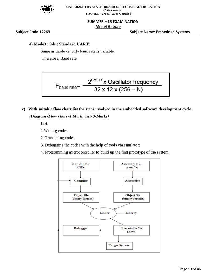
MAHARASHTRA STATE BOARD OF TECHNICAL EDUCATION (Autonomous)
(ISOIEC - 27001 - 2005 Certified)
SUMMER ndash 13 EXAMINATION Model Answer
Subject Code12269 Subject Name Embedded Systems
Page 15 of 46
e) Describe task management with task State transition diagram
(Task management 2-Marks state transition diagram 2-Marks)
Task management
Task management is the process of managing tasks through its life cycle It involves planning
testing tracking and reporting Task management can help either individuals achieve goals or groups
of individuals collaborate and share knowledge for the accomplishment of collective goals[1]
Tasks
are also differentiated by complexity from low to high Effective task management requires
managing all aspects of a task including its status priority time human and financial resources
assignments recurrences notifications and so on These can be lumped together broadly into the
basic activities of task management Managing multiple individual or team tasks may require
specialized task management software Specific software dimensions support common task
management activities These dimensions exist across software products and services and fit different
task management initiatives in a number of ways In fact many people believe that task management
should serve as a foundation for project management activities Task management may form part of
project management and process management and can serve as the foundation for efficient workflow
in an organisation Project managers adhering to task-oriented management have a detailed and up-to-
date project schedule and are usually good at directing team members and moving the project
forward
State Transistion diagram for MOD5 counter
For example the state transition diagram corresponding to the modulo-5 counter is shown in Figure
State transition diagram of a counter
MAHARASHTRA STATE BOARD OF TECHNICAL EDUCATION (Autonomous)
(ISOIEC - 27001 - 2005 Certified)
SUMMER ndash 13 EXAMINATION Model Answer
Subject Code12269 Subject Name Embedded Systems
Page 16 of 46
Q3 Attempt any FOUR of the following MARKS 16
a) Explain the ports of 8051 microcontroller used for External memory access
(PORT 0 Explanations - 2 Marks)
(PORT 2 Explanations - 2 Marks)
Port 0
Port-0 can be configured as a normal bidirectional IO port or it can be used for addressdata
interfacing for accessing external memory When control is 1 the port is used for addressdata
interfacing When the control is 0 the port can be used as a normal bidirectional IO port
Port-2
Port-2 is used for higher external address byte or a normal inputoutput port The IO operation is
similar to Port-1 Port-2 latch remains stable when Port-2 pin are used for external memory access
Here again due to internal pull-up there is limited current driving capability
MAHARASHTRA STATE BOARD OF TECHNICAL EDUCATION (Autonomous)
(ISOIEC - 27001 - 2005 Certified)
SUMMER ndash 13 EXAMINATION Model Answer
Subject Code12269 Subject Name Embedded Systems
Page 17 of 46
b) Draw the block diagram of ARM7 TDMI processor Give its features
(Block Diagram - 2 Marks)
(Features - 2 Marks)
Block diagram of ARM7 TDMI processor
Features
1 Von Neumann Architecture
2 3-stage pipeline fetch decode execute
3 32-bit Data Bus
4 32-bit Address Bus
5 37 32-bit registers
6 32-bit ARM instruction set
7 16-bit THUMB instruction set
8 32 X 8 Multiplier
9 Barrel Shifter
MAHARASHTRA STATE BOARD OF TECHNICAL EDUCATION (Autonomous)
(ISOIEC - 27001 - 2005 Certified)
SUMMER ndash 13 EXAMINATION Model Answer
Subject Code12269 Subject Name Embedded Systems
Page 18 of 46
c) Describe any four advantages of embedded system
(1 Marks for each point (Any 4 points))
1) Design and Efficiency
The central processing core in embedded system is generally less complicated making it easier to
design
The limited function required of embedded system allows them to design to most efficiently perform
their function
2) Cost
The streamline make-up of most embedded system allows their parts to be smaller less expensive to
produce
3) Accessibility
If something goes wrong with certain embedded systems they can be too inaccessible to repair This
problem is addressed in the design stage so by programming an embedded system So that it will not
affect related system negatively when malfunctioning
4) Maintenance
Embedded systems are easier to maintain because the supplied power is embedded in the system and
does not required remote maintenance
5) Redundancies
Embedded system does not involve the redundant programming
d) Write a program in assembly or C language to rotate a stepper motor 1800 in the clockwise
direction The motor has step angle of 180
Use 4 step sequence
(1 Marks for count for 4-step sequence)
(3 Marks for programming)
step-angle of stepper motor = 180
Total no‟s of step required = 18018 = (100)
We are sending 4 pulses and then checking counter So counter is 1004 = 25
A B C D
1 0 0 1 =09 D COIL
1 1 0 0 =0C C COIL
0 1 1 0 =06 B COIL
MAHARASHTRA STATE BOARD OF TECHNICAL EDUCATION (Autonomous)
(ISOIEC - 27001 - 2005 Certified)
SUMMER ndash 13 EXAMINATION Model Answer
Subject Code12269 Subject Name Embedded Systems
Page 19 of 46
0 0 1 1 =03 A COIL
PROGRAM STEPPER MOTOR DRIVER USING LOOKUP TABLE
ORG 0000H START THE PROGRAM
MOV R6 25 TAKE COUNTER FOR 180O ROTATION
UPX MOV DPTR0400H LOAD THE STARTING ADDRESS OF LOOKUP TABLE
MOV R704H LOAD THE COUNTER
H CLR A CLEAR THE A
MOVC AA+DPTR TAKE THE CODE FROM LOOKUP TABLE
MOV P0A SEND THE CODE TO P0
INC DPTR INCREMENT DPTR FOR NEXT CODE
LCALL DELAY DELAY
DJNZ R7H DECREMENT THE COUNTER
DJNZ R6UPX REPEAT UNTIL 180O ROTATION
HERE SJMP HERE STOP PROGRAM AFTER 180O ROTATION
ORG 0400H STARTING ADDRESS OF LOOKUP TABLE
DB 09H 0400H = 09H
DB 0CH 0401H = 0CH
DB 06H 0402H = 06H
DB 03H 0403H = 03H
DELAY DELAY LOOP WITIN LOOP
MOV R001FH
UP2 MOV R10FFH
UP1 DJNZ R1UP1
DJNZ R0UP2
RET
MAHARASHTRA STATE BOARD OF TECHNICAL EDUCATION (Autonomous)
(ISOIEC - 27001 - 2005 Certified)
SUMMER ndash 13 EXAMINATION Model Answer
Subject Code12269 Subject Name Embedded Systems
Page 20 of 46
Alternate program in assembly
PROGRAM SIMPLE STEPPER MOTOR DRIVER USING ROTATE INSTRUCTION
COUNTER FOR 180O IS 100
ORG 0000H START THE PROGRAM
MOV R6100 SET COUNTER = 100 FOR 100 PULSES = 180O
MOV A0EEH LOAD THE CODE TO DRIVE THE MOTOR
UP MOV P0A SEND CODE TO P0
LCALL DELAY DELAY
RR A ROTATE THE CODE
DJNZ R6UP REPEAT THE STEPS
HERE SJMP HERE STOP PROGRAM AFTER 180O ROTATION
DELAY DELAY LOOP WITIN LOOP
MOV R001FH
UP2 MOV R10FFH
UP1 DJNZ R1UP1
DJNZ R0UP2
RET
C language program Stepper motor interfacing
include ltIntel8052hgt
include ltstandardhgt
COIL A = P00
COIL B = P01
COIL C = P02
COIL D = P03
void main ()
MAHARASHTRA STATE BOARD OF TECHNICAL EDUCATION (Autonomous)
(ISOIEC - 27001 - 2005 Certified)
SUMMER ndash 13 EXAMINATION Model Answer
Subject Code12269 Subject Name Embedded Systems
Page 21 of 46
P0 = 0xFF MOTOR OFF
For (x=100 x=0 x=x-4)
P0 = 0x09 COIL A ON
delay_ms (100)
P0 = 0x0C COIL B ON
delay_ms (100)
P0 = 0x06 COIL C ON
delay_ms (100)
P0 = 0x03 COIL D ON
delay_ms (100)
[NOTE Program may change Student can also use the other logic]
[Please check the logic and understanding of students]
MAHARASHTRA STATE BOARD OF TECHNICAL EDUCATION (Autonomous)
(ISOIEC - 27001 - 2005 Certified)
SUMMER ndash 13 EXAMINATION Model Answer
Subject Code12269 Subject Name Embedded Systems
Page 22 of 46
e) Draw interfacing diagram of 7 segment LED display with 8051 microcontroller
(Neat and labeled diagram - 4 Marks)
INTERFACING OF 7 SEGMENT LED DISPLAY WITH 8051 MICROCONTROLLER
MAHARASHTRA STATE BOARD OF TECHNICAL EDUCATION (Autonomous)
(ISOIEC - 27001 - 2005 Certified)
SUMMER ndash 13 EXAMINATION Model Answer
Subject Code12269 Subject Name Embedded Systems
Page 23 of 46
Q4a) Attempt any THREE of the following MARKS 12
i ) Draw and explain the formats of SFR‟s
1) SCON
2) PCON
( Each Format 01 Mark amp Each Explanation 01 Mark)
Serial Port Control (SCON) Register
SM0 - Serial port mode bit 0 is used for serial port mode selection
SM1 - Serial port mode bit 1 is used for serial port mode selection
SM2 - Serial port mode 2 bit also known as multiprocessor communication enable bit When set it
enables multiprocessor communication in mode 2 and 3 and eventually mode 1 It should be cleared
in mode 0
REN - Reception Enable bit enables serial reception when set When cleared serial reception is
disabled
TB8 - Transmitter bit 8 Since all registers are 8-bit wide this bit solves the problem of transmitting
the 9th bit in modes 2 and 3 It is set to transmit a logic 1 in the 9th bit
RB8 - Receiver bit 8 or the 9th bit received in modes 2 and 3 Cleared by hardware if 9th bit received
is a logic 0 Set by hardware if 9th bit received is a logic 1
TI - Transmit Interrupt flag is automatically set at the moment the last bit of one byte is sent Its a
signal to the processor that the line is available for a new byte transmit It must be cleared from within
the software
RI - Receive Interrupt flag is automatically set upon one byte receive It signals that byte is received
and should be read quickly prior to being replaced by a new data This bit is also cleared from within
the software
MAHARASHTRA STATE BOARD OF TECHNICAL EDUCATION (Autonomous)
(ISOIEC - 27001 - 2005 Certified)
SUMMER ndash 13 EXAMINATION Model Answer
Subject Code12269 Subject Name Embedded Systems
Page 24 of 46
PCON register
The purpose of the Register PCON bits is
SMOD Baud rate is twice as much higher by setting this bit
GF1 General-purpose bit (available for use)
GF0 General-purpose bit (available for use)
PD By setting this bit the microcontroller enters the Power Down mode
IDL By setting this bit the microcontroller enters the Idle mode
ii) Draw pinout of 14 pin LCD display and state the functions of
1)RS
2) EN
3) RW
(Pin out diagram 01 Mark Explanations of each pin 01 Mark)
Pin out diagram of 14 pin LCD
Explanation of RS RW and EN
RS - RS is used to make the selection between data and command register
RS=0 command register is selected
RS=1 data register is selected
MAHARASHTRA STATE BOARD OF TECHNICAL EDUCATION (Autonomous)
(ISOIEC - 27001 - 2005 Certified)
SUMMER ndash 13 EXAMINATION Model Answer
Subject Code12269 Subject Name Embedded Systems
Page 25 of 46
RW- RW gives you the choice between writing and reading
RW=1 reading is enabled
RW=0 then writing is enabled
EN - Enable pins is used by the LCD to latch information presented to its data pins
When data is supplied to data pins a high to low pulse must be applied to this pin in-order for
the LCD to latch in the data present at the data pins
iii) Describe dual role of port 0 in 8051 microcontroller
(Role 1 ndash Port 0 as Input or Output ndash 2 Marks)
(Role 2 ndash Port 0 as AD0 to AD7 for external memory ndash 2 Marks)
Port 0 as input or output port
Port 0 occupies a total of 8 pins (pins 32-39) It can be used for input or output To use the pins of port
0 as both input and output ports each pin must be connected externally to a 10K ohm pull-up resistor
This is due to the fact that P0 is an open drain Open drain is a term used for MOS chips in the same
way that open collector is used for TTL chips With external pull-up resistors connected upon reset
port 0 is configured as an input or output port
Port 0 as AD0 to AD7 for external memory access
Port 0 is also designated as AD0-AD7 allowing it to be used for both address and data When
connecting an 805131 to an external memory port 0 provides both address and data The 8051
multiplexes address and data through port 0 to save pins ALE indicates if P0 has address or data
When ALE = 0 it provides data D0-D7 but when ALE =1 it has address and data with the help of a
74LS373 latch
MAHARASHTRA STATE BOARD OF TECHNICAL EDUCATION (Autonomous)
(ISOIEC - 27001 - 2005 Certified)
SUMMER ndash 13 EXAMINATION Model Answer
Subject Code12269 Subject Name Embedded Systems
Page 26 of 46
iv) Write assembly or bdquoC‟ language program to transfer the message ldquoMSBTErdquo serially at baud
rate 4800 8 bit data 1 stop bit
(Calculation for Baud rate ndash 1marks and Correct Program 03 Marks)
Calculation for baud rate
[Note In question no crystal value is given So students can assume any crystal value and will do
calculations]
We are assuming crystal value 110592 MHz
o Timer clock Frequency is = XTAL 12
= 110592MHz 12
= 9216 KHz
o UART Frequency is = Timer clock Frequency 32
= 9216KHz 32
= 288 KHz
o Baud rate = UART Frequency COUNTER Value
o COUNTER Value = UART Frequency Baud Rate
= 288 KHz 4800
= 6
As timer in microcontroller is up counter timer so counter value is = -6
ASSEMBLY LANGUAGE PROGRAM - SINGLE CHARACTER TRANSMISSION
MOV TMOD20H TIMER 1 MODE 2
MOV TH1-6 4800 BAUD RATE
MOV SCON50H 8 BIT UART 1 Start bit ndash 8 data bit ndash 1 stop Bit
SETB TR1 start timer1
MOV SBUF ldquoMrdquo send M
WAIT JNB TIWAIT
CLR TI
MOV SBUF ldquoSrdquo send S
WAIT1 JNB TIWAIT1
CLR TI
MOV SBUF ldquoBrdquo send B
MAHARASHTRA STATE BOARD OF TECHNICAL EDUCATION (Autonomous)
(ISOIEC - 27001 - 2005 Certified)
SUMMER ndash 13 EXAMINATION Model Answer
Subject Code12269 Subject Name Embedded Systems
Page 27 of 46
WAIT2 JNB TIWAIT2
CLR TI
MOV SBUF ldquoTrdquo send T
WAIT3 JNB TIWAIT3
CLR TI
MOV SBUF ldquoErdquo send E
WAIT4 JNB TIWAIT4
CLR TI
HERE SJMP HERE
ALTERNATE PROGRAM BY STRING
MOV TMOD 20H
MOV TH1 -6
MOV SCON 50H
MOV DPTR MESSAGE
MOV R0 5
SETB TR1
REPT CLR A
MOVC A A+DPTR
MOV SBUF A
HERE JNB TI HERE
INC DPTR
CLR TI
DJNZ R0 REPT
MESSAGE DB bdquoMSBTE‟ 0
END
MAHARASHTRA STATE BOARD OF TECHNICAL EDUCATION (Autonomous)
(ISOIEC - 27001 - 2005 Certified)
SUMMER ndash 13 EXAMINATION Model Answer
Subject Code12269 Subject Name Embedded Systems
Page 28 of 46
C Language Program
This program uses the on-chip serial port as the standard output device and sends MSBTE
message to it
Initialize Serial Port
It initializes serial port in Mode 1 for 4800 baud rate generated using Timer 1 110592 MHz
include ltIntel8051hgt
include ltstdiohgt
void main ()
TH1 = 0xfa LOAD COUNTER FDH IE 03H
TL1 = 0xfa
PCON amp= 0x7f SMOD = 0
SCON = 0x50 SET UART IN MODE 1 IE 1 START 8 DATA 1 STOP
TMOD = 0x20 SET TMOD IN MODE 2 IE AUTO RELOAD MODE
TCON = 0x40 START TIMER
while(1)
printf( MSBTE n)
delay_ms(1000)
b) Attempt any ONE of the following MARKS 6
i) Explain the various Hardware and software development tools used in embedded system
(Any three Hardware tools with explanation 03 Marks)
(Any three software tools with explanation 03 Marks)
Various software development tools in embedded systems are-
1 Compiler
2 Cross assembler
3 Cross compiler
4 Locators
MAHARASHTRA STATE BOARD OF TECHNICAL EDUCATION (Autonomous)
(ISOIEC - 27001 - 2005 Certified)
SUMMER ndash 13 EXAMINATION Model Answer
Subject Code12269 Subject Name Embedded Systems
Page 29 of 46
5 Loaders
6 Simulators
7 Debugger
8 Integrated development environment (IDE)
Compiler- It is a computer program that transforms the source code written in a programming or
source language into another computer language ie target language ie binary code known as object
code
Cross assembler-It is useful to convert object codes for microcontrollers or processor to other codes
for another microcontrollers or processor and vice versa
Cross compiler- It is used to create executable code other than one on which the compiler is run
They are used to generate executables for embedded systems or multiple platforms
LinkerLocator- It is used for relocation process It is done during compilation also it can be done at
run time by a relocating loader It is a program that takes one or more objects generated by compiler
and combines them into a single executable program
Simulators- A simulator is the sw that simulates a hw unit like emulator peripheral network and
IO devices on a PC
It defines a processor or processing device as well as various versions for the target system
Monitors the detailed information of as source code part with labels and symbols during the
execution for each single step
Provides the detailed information of the status of memory RAM and simulated ports simulated
peripheral devices of the defined target system
Integrated Development Environment (IDE) -
It supports for defining a processor family and its version
Support a user definable assembler to support a new version or a type of processor
Provides multiuser environment
MAHARASHTRA STATE BOARD OF TECHNICAL EDUCATION (Autonomous)
(ISOIEC - 27001 - 2005 Certified)
SUMMER ndash 13 EXAMINATION Model Answer
Subject Code12269 Subject Name Embedded Systems
Page 30 of 46
Supports conditional and unconditional break points
Provide debugger
Various Hardware development tools in embedded systems are-
1 Emulators
2 In-Circuit emulators (ICE)
3 Target board
4 Device programmer
Emulator- It duplicates the functions of one system using a different system so that the second
system behaves like the first system A hardware emulator is an emulator which takes the form of hard
ware device
Emulators maintain the original look feel and behavior of the digital object as digital data itself
Reduces labor hours
It allows video games exclusive to one system to be played on another
In ndashCircuit Emulator (ICE )-
It is a hardware device used to debug the sw of an embedded system
It provides a window into the embedded system The programmer uses the emulator to load
programs into the embedded system run them and view and change data used by the systems sw
It emulates the CPU of the embedded systems computer
Recent ICEs enable a programmer to access the on chip debug circuit that is integrated into the
CPU via JTAG or BDM in order to debug the sw of an embedded system
Target Board -
It has a processor ie microprocessor or microcontroller memory for image of the embedded sw ie
ROM memory for the implementation of the stack temporary variables and memory buffers ie
RAM peripheral devices and interfaces such as RS 232 10100-base Ethernet parallel ports USB
port etc
It consists microcontroller 8051 Monitor flash memory RAM Serial Ports parallel ports
system keyboard system display etc
Device Programmer-
It is the hardware tool used to burn ie Load the hex or bin file into Microcontroller
MAHARASHTRA STATE BOARD OF TECHNICAL EDUCATION (Autonomous)
(ISOIEC - 27001 - 2005 Certified)
SUMMER ndash 13 EXAMINATION Model Answer
Subject Code12269 Subject Name Embedded Systems
Page 31 of 46
ii) Draw the circuit diagram to interface 4x4 matrix keyboards with 8051 microcontroller What
are the steps to detect key press
(Interfacing Diagram- 02 Marks Steps- 04 Marks)
Circuit Diagram
Steps to detect key press
1 To make sure that preceding key has been released0s are output to all rows at once and the
columns are read and checked repeatedly until all columns are high When all columns are found
to be high the program bits for a short amount of time before it go to the next stage of waiting for
a key to be pressed
2 To see if any key pressed the columns are scan over and over in an infinite loop until one of them
has a 0 on it Remember that the output latches connected to row still have there initial zeros
(provided in stage one) making them grounded After the key press detection the microcontroller
bits 20 msec for the bounce and then scan the columns again this serve to functions (A) it ensure
that the first key press detection was not an erroneous one due to spike noise and (B) the 20 msec
delay prevents the same key pressed from being interpreted as multiple key press If after the
MAHARASHTRA STATE BOARD OF TECHNICAL EDUCATION (Autonomous)
(ISOIEC - 27001 - 2005 Certified)
SUMMER ndash 13 EXAMINATION Model Answer
Subject Code12269 Subject Name Embedded Systems
Page 32 of 46
20msec delay the key is still pressed its goes to the next stage to detect which row it belongs to
otherwise it goes back into the loop to detect a real key press
3 To detect which row the key press belongs to the microcontroller grounds one row at a time
reading the columns each time If it finds that all columns are high this means that the key press
cannot belong to that row therefore it ground the next row and continues until it finds the row the
key press belongs to Upon finding the row that the key press belongs to it sets up the starting
address for the look-up table holding the scan codes (or the ASCII value) for that row and goes to
the next stage to identify the key
4 To identify the key press the microcontroller rotates the columns bit at a time into the carry flag
and checks to see if it is low Upon finding the zero it pulls out the ASCII code for that key from
the look ndashup table otherwise it increment the pointer to point to the next element of the look-up
table
Q5 Attempt any TWO of the following MARKS 16
a) Draw the labeled diagram of interfacing DAC with 8051 Microcontroller Write a program in
assembly or bdquoC‟ language to generate a sawtooth waveform
(Neat and labeled diagram - 4 Marks)
(Correct program in Assembly or lsquoCrsquo - 4 Marks)
Circuit Diagram of interfacing DAC with 8051 Microcontroller
MAHARASHTRA STATE BOARD OF TECHNICAL EDUCATION (Autonomous)
(ISOIEC - 27001 - 2005 Certified)
SUMMER ndash 13 EXAMINATION Model Answer
Subject Code12269 Subject Name Embedded Systems
Page 33 of 46
Assembly Language Program to generate Sawtooth waveform
ORG 0000H START THE PROGRAM
MOV A00H LOAD A=00H
UP MOV P1A SEND A TO P0
INC A INCEREMENT A
NOP DELAY
SJMP UP REPEAT THE PROCEDURE
C language program GENERATING SAWTOOTH WAVE USING DAC0808
P1 = DAC D0 TO D7
include ltIntel8052hgt
include ltstandardhgt
unsigned char c
void main ()
while (1)
for (c=0clt256c++)
P1 = c
delay_ms(10)
MAHARASHTRA STATE BOARD OF TECHNICAL EDUCATION (Autonomous)
(ISOIEC - 27001 - 2005 Certified)
SUMMER ndash 13 EXAMINATION Model Answer
Subject Code12269 Subject Name Embedded Systems
Page 34 of 46
b) Draw and explain the format of IE and TCON SFR Which bits in which SFR‟s must be
manipulated to make INT0 level activated and INT1 edge activated
(IE format - 1 Marks)
(IE format explanation - 2 Marks)
(TCON format - 1 Mark)
(TCON format explanation - 2 Marks)
(Bit Manipulation for INT0 level activated ndash 1 Mark)
(Bit Manipulation for INT1 Edge activated ndash 1 Mark)
IE Format
IE format explanation
EA - global interrupt enabledisable
0 - disables all interrupt requests
1 - enables all individual interrupt requests
ES - enables or disables serial interrupt
0 - UART system cannot generate an interrupt
1 - UART system enables an interrupt
ET1 - bit enables or disables Timer 1 interrupt
0 - Timer 1 cannot generate an interrupt
1 - Timer 1 enables an interrupt
EX1 - bit enables or disables external 1 interrupt
0 - change of the pin INT0 logic state cannot generate an interrupt
1 - enables an external interrupt on the pin INT0 state change
ET0 - bit enables or disables timer 0 interrupt
0 - Timer 0 cannot generate an interrupt
1 - enables timer 0 interrupt
EX0 - bit enables or disables external 0 interrupt
0 - change of the INT1 pin logic state cannot generate an interrupt
1 - enables an external interrupt on the pin INT1 state change
MAHARASHTRA STATE BOARD OF TECHNICAL EDUCATION (Autonomous)
(ISOIEC - 27001 - 2005 Certified)
SUMMER ndash 13 EXAMINATION Model Answer
Subject Code12269 Subject Name Embedded Systems
Page 35 of 46
TCON Format
TCON Format explanation
TF1 - TCON 7 - Timer 1 overflow flag Set by hardware when the TimerCounter 1 overflows
Cleared by hardware as processor vectors to the interrupt service routine
TR1 - TCON 6 - Timer 1 run control bit Setcleared by software to turn TimerCounter 1
ONOFF
TF0 - TCON 5 - Timer 0 overflow flag Set by hardware when the TimerCounter 0 overflows
Cleared by hardware as processor vectors to the service routine
TR0 - TCON 4 - Timer 0 run control bit Setcleared by software to turn TimerCounter 0
ONOFF
IE1 - TCON 3 - External Interrupt 1 edge flag Set by hardware when External Interrupt edge is
detected Cleared by hardware when interrupt is processed
IT1 - TCON 2 - Interrupt 1 type control bit Setcleared by software to specify falling edgelow
level triggered External Interrupt
IE0 - TCON 1 - External Interrupt 0 edge flag Set by hardware when External Interrupt edge
detected Cleared by hardware when interrupt is processed
IT0 - TCON 0 - Interrupt 0 type control bit Setcleared by software to specify falling edgelow
level triggered External Interrupt
Bit Manipulation for INT0 level activated
To make INT0 level triggered the IT0 ie TCON0 bit of TCON SFR must be manipulated
TCON0 = 0 - INT0 level triggered
Bit Manipulation for INT1 Edge activated
To make INT1 Edge triggered the IT1 ie TCON2 bit of TCON SFR must be manipulated
TCON2 = 1 - INT1 Edge triggered
MAHARASHTRA STATE BOARD OF TECHNICAL EDUCATION (Autonomous)
(ISOIEC - 27001 - 2005 Certified)
SUMMER ndash 13 EXAMINATION Model Answer
Subject Code12269 Subject Name Embedded Systems
Page 36 of 46
c) Draw the diagram to interface 16X2 LCD display with 8051 microcontroller Compare LCD
module interface with 7 segment LET multiplex interface based on the following points
i) Hardware requirement for displaying 16 characters
ii) Refreshing the display
iii) Power Consumption
iv) Software Complexity
(Interface diagram of 16X2 LCD with 8051 -2 Marks)
(Each Difference point- 1frac12 Marks)
Interface diagram of 16X2 LCD with 8051
MAHARASHTRA STATE BOARD OF TECHNICAL EDUCATION (Autonomous)
(ISOIEC - 27001 - 2005 Certified)
SUMMER ndash 13 EXAMINATION Model Answer
Subject Code12269 Subject Name Embedded Systems
Page 37 of 46
Sr
No
Point 16X2 LCD Multiplexed 7 Segment LED
Display
1 Hardware
requirement for
displaying 16
characters
Single 16X2 display is used to
display 32 characters So
hardware requirement is
less
16 seven segments are required
to display 16 characters at a
time Therefore hardware
requirement is more
2 Refreshing the
display
In LCD the characters are
stored in RAM therefore no
refreshing is required
In multiplexed 7 segment
displays No RAM is used
therefore refreshing the
display is required It is
compulsory
3 Power
Consumption
LCD 16X2display requires
less power
7 Segment display requires
more power
4 Software
Complexity
Software for LCD
interfacing is simple
Software for 7 segment
multiplexed display is
complex
MAHARASHTRA STATE BOARD OF TECHNICAL EDUCATION (Autonomous)
(ISOIEC - 27001 - 2005 Certified)
SUMMER ndash 13 EXAMINATION Model Answer
Subject Code12269 Subject Name Embedded Systems
Page 38 of 46
Q6 Attempt any FOUR of the following MARKS 16
a) Write a program in assembly or bdquoC‟ language to generate a square wave of 1 KHz with 50
duty cycle on P15 pin of 8051 microcontroller Use timer 0 to generate the delay
(Calculations --- 2 Marks)
(Program --- 2 Marks)
[Note In question no crystal value is given So students can assume any crystal value and will do
calculations]
We are assuming crystal value 110592 MHz
o Look at the following steps for 1 KHz frequency calculations with 110592 MHz
o The period of the square wave = 1 1 KHz
= 1 ms
o The high or low portion of the square wave = Time period 2
= 1ms 2
= 05 ms
= 500uSec
o Timer clock Frequency is = XTAL 12
= 110592MHz 12
= 9216 KHz
o Timer clock period is = 1 Timer Frequency
= 1 9216 KHz
= 1085 uSec
o Counter = Delay timer clock period
=500 uSec 1085 uSec
= 461
o Timer Reload value = Maximum Count ndash Counter
= 65536 ndash 461
= (65075)d
o Timer Reload value in HEX = (65075)d
= (FE33) h
o TL0 = 33 h and TH0 = FE h
MAHARASHTRA STATE BOARD OF TECHNICAL EDUCATION (Autonomous)
(ISOIEC - 27001 - 2005 Certified)
SUMMER ndash 13 EXAMINATION Model Answer
Subject Code12269 Subject Name Embedded Systems
Page 39 of 46
Assembly program to generate square wave over Port Pin P15 using timer 0
ORG 0000H Start the program
REPEAT CPL P23 compliment the P23
LCALL DELAY delay of 10 ms for 50Hz
SJMP REPEAT repeat the process
DELAY MOV TMOD01H timer 1 mode 1
MOV TL033H Timer value = DC00H
MOV TH00FEH
SETB TR0 start the timer
BACK JNB TF0BACK wait until TF1 sets
CLR TR0 stop
CLR TF0 clear timer flag 1
RET
C language program to generate square wave over Port Pin P15 using timer 0
include ltIntel8052hgt
include ltstandardhgt
Void T0M1delay(void) Timer 0 Mode 1(16 bit timer)
BIT OUTPUT P15 Initialize Port pin P15
void main ()
while (1)
OUTPUT= ~ OUTPUT toggle P15
T0M1delay() delay of 500 uSec
Void T0M1delay() Timer 0 Mode 1(16 bit timer) - delay of 500 uSec
TMOD = 0x01 Timer 0 Mode 1(16 bit timer)
TL0 = 0x33 Load TL0 = 33h
MAHARASHTRA STATE BOARD OF TECHNICAL EDUCATION (Autonomous)
(ISOIEC - 27001 - 2005 Certified)
SUMMER ndash 13 EXAMINATION Model Answer
Subject Code12269 Subject Name Embedded Systems
Page 40 of 46
TH0 = 0xFE Load TL0 = FEh
TR0 = 1 Run the timer 0
while (TF0 = = 0) Wait for TF0 to overflow
TR0 = 0 Stop the timer 0
TF0 = 1 Clear TF0
b) Draw and explain I2C serial bus Protocol
(I2C Explanation --- 2 Marks)
(I2C Protocol diagram --- 2 Marks)
I2C Serial Bus Protocol
o I2C is well known bus invented by PHILIPS
o I2C stands for INTER-INTEGRATED CIRCUIT
o It has speed of 100kbs but it can be extended to 450kbps
o The I2C Bus has two lines that carry its signals minus one line is for clock named as SCL and
second is for data named as SDL
o By using I2C protocol the master can address 127 slaves at an instance
o It has a processing element functionally as a bus controller or a microcontroller with I2C bus
interface circuits
MAHARASHTRA STATE BOARD OF TECHNICAL EDUCATION (Autonomous)
(ISOIEC - 27001 - 2005 Certified)
SUMMER ndash 13 EXAMINATION Model Answer
Subject Code12269 Subject Name Embedded Systems
Page 41 of 46
Bits as per I2C Bus Protocol
First field of 1 bit Start bit similar to one in an UART
Second field of 7 bits address field It defines the slave address which is being sent the data
frame (of many bytes) by the master
Third field of 1 control bit defines whether a read or write cycle is in progress
Fourth field of 1 control bit defines whether is the present data is an acknowledgment
(from slave)
Fifth field of 8 bits I2C device data byte
Sixth field of 1-bit bit NACK (negative acknowledgement) from the receiver If active then
acknowledgment after a transfer is not needed from the slave else acknowledgement is
expected from the slave
Seventh field of 1 bit stop bit
MAHARASHTRA STATE BOARD OF TECHNICAL EDUCATION (Autonomous)
(ISOIEC - 27001 - 2005 Certified)
SUMMER ndash 13 EXAMINATION Model Answer
Subject Code12269 Subject Name Embedded Systems
Page 42 of 46
c) What are the different types of advance serial and parallel high speed bus Explain any one
parallel high speed bus in detail
(Serial Bus --- 1 Mark)
(Parallel Bus --- 1 Mark)
(Explanation on any 1 Parallel Bus --- 2 Marks)
Serial Bus
o RS232
o I2C
o CAN
o RS422
o USB
o Fire wire
o Infrared
o IEEE 80211 Wireless (Wifi)
o Blue Tooth
o VOIP
Parallel Bus
o PCI Bus
o PCI-X Bus
o ARM Bus
1) PCI and PCI-X bus
Recently the most used synchronous parallel bus in the computer systems for interfacing PC-
based device is PCI (Peripheral Component Interconnect)
o Features
1 Plat form independent unlike ISA which needs an IBM platform
2 Clock rate is submultiples of system clock
3 Its versions are 3233 MHz6466 MHz PCI-X 64100 MHzPCI super v23 264528 Mbps 33v
can a 64-bits bus)132264 (on a 32-bit bus) amp PCI-X super V101a for 800 Mbps 64-bits bus 33v
4 A PCI driver can access hardware automatically as well as bus addresses assigned by the
programmer
MAHARASHTRA STATE BOARD OF TECHNICAL EDUCATION (Autonomous)
(ISOIEC - 27001 - 2005 Certified)
SUMMER ndash 13 EXAMINATION Model Answer
Subject Code12269 Subject Name Embedded Systems
Page 43 of 46
5 PCI-X is an extension of PCI bus amp Supports 64100 MHz transfers
2) ARM BUS
ARM Processor interfaces the memory external DRAM controller amp on chip IO devices which
connect to 32 bit data amp 32 bit address line at high speed using AMBA(ARM Main Memory BUS
Architecture) - AHB(ARM High Performance Bus)
o ARM bus is of two types
AMBA-AHB connects to high speed memory
AMBA-APB connects the external peripherals to the systems memory bus through a bridge
o Following are advanced bus standards
1GMIT (Gigabit Ethernet MAC Interchange Interface)
2XGMI (10 Gigabit Ethernet MAC Interchange Interface)
3CSIX-166 Gbps 32 bit HSTL with 200mhz performance
4Rapid IO interconnect Specification V11 at 8 Gbps with 500 Mbps performance or 250 MHz
dual direction registering performance using 8-bit LVDS (Low Voltage Data Bus
d) With one suitable example describe the concept of device driver
(Concept of device driver --- 3 Marks)
(Any Example --- 1 Mark)
Concept of Device driver
o A device driver is a software routine allowing a higher level computer program to interact with a
hardware device
o The device driver has software routines that provide the functionality of an input output IO
device
o The driver communicates with the device through the computer bus or subsystem The driver
issues commands to the device when a driver routine is invoked
o The device then sends the data back to the driver for the driver to invoked routine in the calling
program if required
MAHARASHTRA STATE BOARD OF TECHNICAL EDUCATION (Autonomous)
(ISOIEC - 27001 - 2005 Certified)
SUMMER ndash 13 EXAMINATION Model Answer
Subject Code12269 Subject Name Embedded Systems
Page 44 of 46
o Drivers are hardware dependant and operating system specific A device driver simplifies
programming by acting as a layer between the device and the operating system or the application
program
o Any system which has devices will need device drivers therefore the embedded software
programmer must design codes for
Device Initialization
Device activation
Device driving using interrupt service routine
Resetting or device deactivation
Example (Student can give any example)
Coffee vending machine
o Device collects coin at input port
o The system now awakens and activates on interrupt to execute a service routine
o This is the device driver routine for that input port
e) State any four specifications and four applications of RTOS
(Four specifications --- 2 Marks)
(Four applications --- 2 Mark)
Specifications of RTOS
o Reliability The RTOS is reliable because it is available for all time and normally it does not
fail to perform any functionoperation The reliability of system also depends on the
hardware board support package and application code
o Predictability In RTOS the user knows within How much time period the RTOS is going to
perform the task ie The RTOS has predictability We can predict determine how much
time takes by RTOS
o Performance The performance of RTOS is very fast so that it can fulfill all timing
requirement
o Compactness The RTOS provide compactness It required less memory space for storage and
hence can be used for portable application like cell phone ECG machine etc
MAHARASHTRA STATE BOARD OF TECHNICAL EDUCATION (Autonomous)
(ISOIEC - 27001 - 2005 Certified)
SUMMER ndash 13 EXAMINATION Model Answer
Subject Code12269 Subject Name Embedded Systems
Page 45 of 46
o Scalability RTOS can be used in a wide variety of embedded They must be able to scale-up
or scale-down to suit the application
Applications of RTOS
o web server
o word processor
o audiovideo media center
o microwave oven
o Fire Alarm System
f) Describe the concept of mutual exclusion and deadlock in RTOS
(Concept of mutual exclusion --- 2 Marks)
(Concept of deadlock --- 2 Marks)
Mutual Exclusion
The easiest way for threads to communicate with each other is through shared data structures This is
especially easy when all threads exist in single address space and can reference global variables
pointers buffers linked lists FIFOs etc
When two or more task access shared resources without corrupting data is called Mutual
Exclusion
It can be performed in the following ways
o Disabling the scheduler
o Disabling the interrupts
o By test and set operation
o Using semaphore
Deadlock
A deadlock also called as deadly embrace is a situation in which two threads are each
unknowingly waiting for resource held by other
o Assume thread T1 has exclusive access to resource R1
o Thread T2 has exclusive access to resource R2
o If T1 needs exclusive access to R2 and T2 needs exclusive access to R1
o Neither thread can continue
o They are deadlocked
MAHARASHTRA STATE BOARD OF TECHNICAL EDUCATION (Autonomous)
(ISOIEC - 27001 - 2005 Certified)
SUMMER ndash 13 EXAMINATION Model Answer
Subject Code12269 Subject Name Embedded Systems
Page 46 of 46
o The simplest way to avoid a deadlock is for threads to
Acquire all resources before proceeding
Acquire the resources in the same order
Release the resource in the revere order
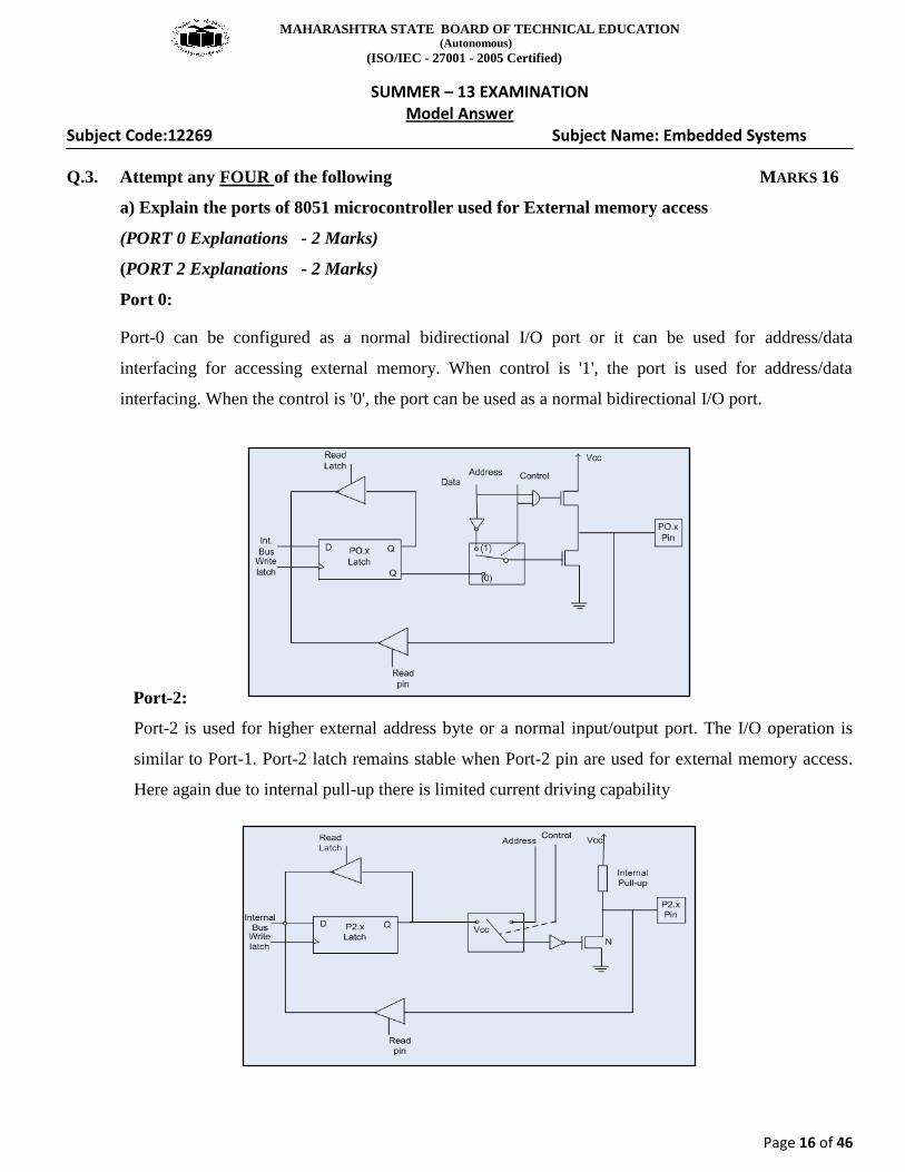
MAHARASHTRA STATE BOARD OF TECHNICAL EDUCATION (Autonomous)
(ISOIEC - 27001 - 2005 Certified)
SUMMER ndash 13 EXAMINATION Model Answer
Subject Code12269 Subject Name Embedded Systems
Page 46 of 46
o The simplest way to avoid a deadlock is for threads to
Acquire all resources before proceeding
Acquire the resources in the same order
Release the resource in the revere order