Embed Size (px)
Citation preview
Mike Mayberry Director of Components Research
VP, Intel Corporation
March 2013
Pushing Past the Frontiers Of Technology
You Are Here – 22nm node
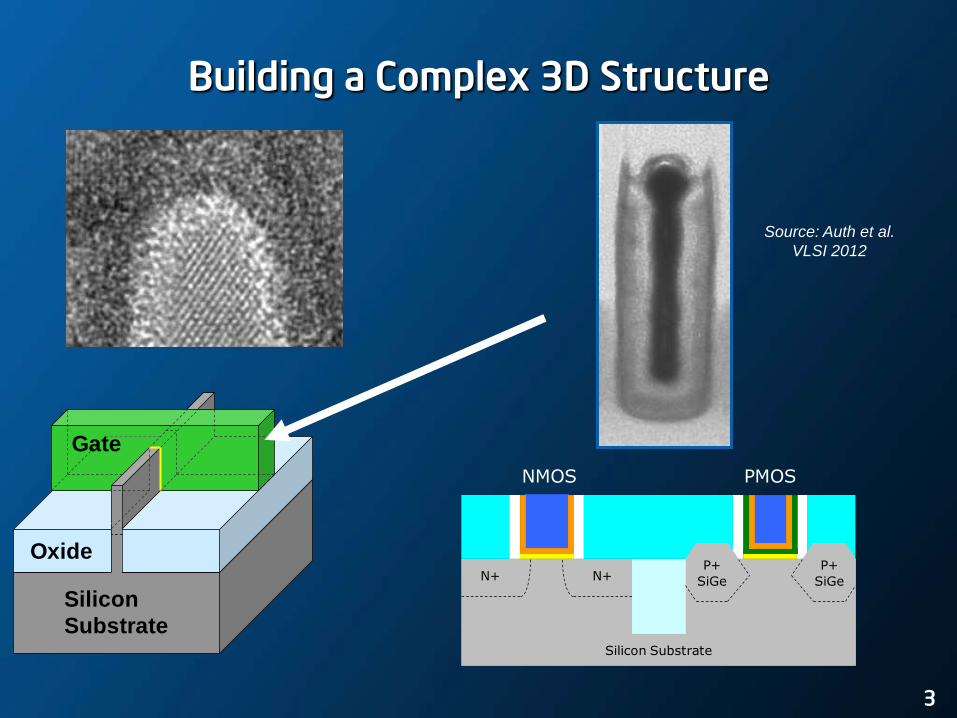
Silicon
Substrate
Oxide
Gate
Building a Complex 3D Structure
P+
SiGe
P+
SiGeN+N+
NMOS PMOS
Silicon Substrate
3
Source: Auth et al.
VLSI 2012
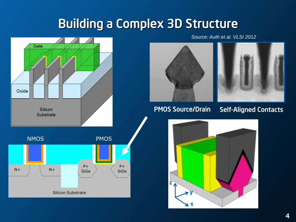
Building a Complex 3D Structure
P+
SiGe
P+
SiGeN+N+
NMOS PMOS
Silicon Substrate
PMOS Source/Drain Self-Aligned Contacts
x
y
z
4
Source: Auth et al. VLSI 2012
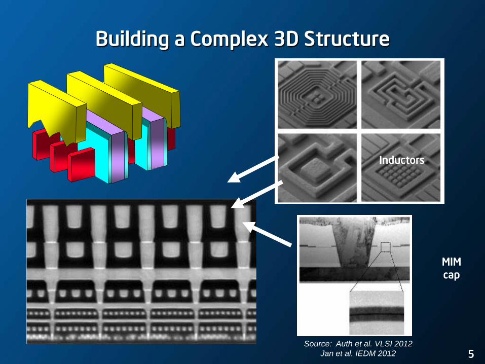
Building a Complex 3D Structure
MIM cap
Inductors
5 Source: Auth et al. VLSI 2012
Jan et al. IEDM 2012
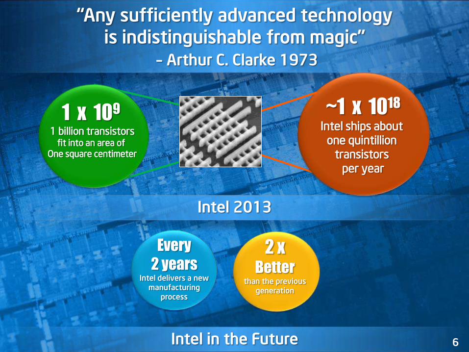
“Any sufficiently advanced technology is indistinguishable from magic”
– Arthur C. Clarke 1973
Intel 2013
~1 x 10¹⁸
Intel ships about
one quintillion
transistors
per year
1 x 10⁹
1 billion transistors fit into an area of
One square centimeter
Every
2 years Intel delivers a new
manufacturing process
2 x Better
than the previous generation
Intel in the Future 6

The (likely) near future
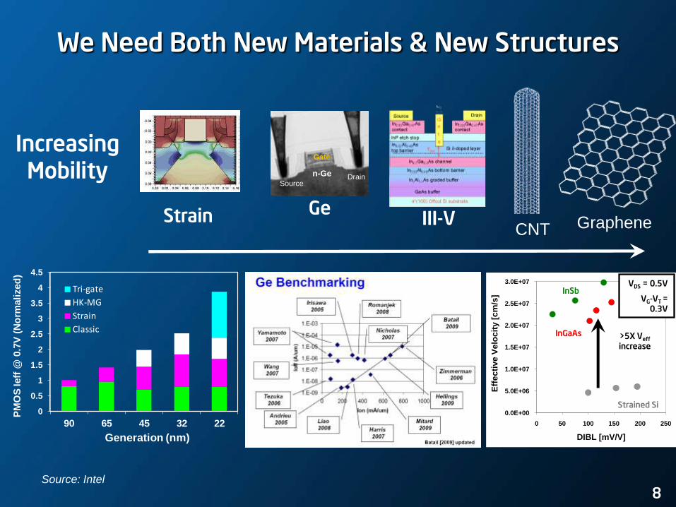
We Need Both New Materials & New Structures
Strain
Increasing Mobility
Graphene CNT
Gate
SourceDrainn-Ge
Gate
SourceDrainn-Ge
Ge
InAlAs Barriers
QW
SEM Micrograph
InP
Energy Band DiagramEnergy Band DiagramEnergy Band Diagram
Si
d
III-V
0.0E+00
5.0E+06
1.0E+07
1.5E+07
2.0E+07
2.5E+07
3.0E+07
0 50 100 150 200 250
DIBL [mV/V]
Eff
ec
tive
Ve
loc
ity [
cm
/s]
InGaAs
Strained Si
InSb
>5X Veff increase
VDS = 0.5V
VG-VT = 0.3V
0
0.5
1
1.5
2
2.5
3
3.5
4
4.5
90 65 45 32 22
PM
OS
Ieff
@ 0
.7V
(N
orm
ali
zed
)
Generation (nm)
Tri-gate
HK-MG
Strain
Classic
8 Source: Intel
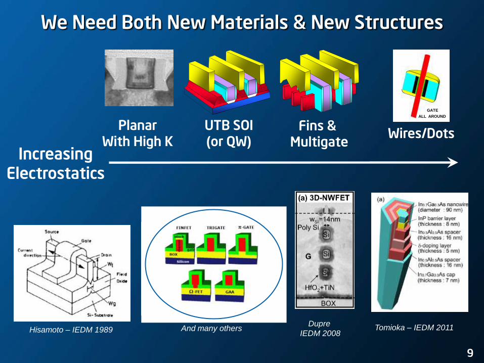
We Need Both New Materials & New Structures
Increasing Electrostatics
Planar With High K
Fins & Multigate
UTB SOI (or QW)
Hisamoto – IEDM 1989
Wires/Dots
Dupre
IEDM 2008 Tomioka – IEDM 2011
GATE
ALL AROUND
And many others
9
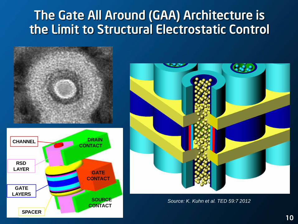
The Gate All Around (GAA) Architecture is the Limit to Structural Electrostatic Control
Source: K. Kuhn et al. TED 59:7 2012
DRAIN
CONTACT
GATE
CONTACT
CHANNEL
RSD
LAYER
GATE
LAYERS
SPACER
SOURCE
CONTACT
10
Modern Technologies are NOT Solely Limited by Transistors
• Interconnections turn devices into useful functions
• 3D structures (finFET’s, vertical FETs, etc.) make this considerably more challenging at 22nm and beyond
• Need thin conformal films for
Gate metals (NMOS and PMOS)
Contact metals
DRAIN
CONTACT
GATE
CONTACT
SOURCE
CONTACT
RACC
RSD
REPI
RSIL
RCON
RINT
RGCON
RGINT
RG1 , RG2 …
DRAIN
CONTACT
GATE
CONTACT
CHANNEL
RSD
LAYER
GATE
LAYERS
SPACER
SOURCE
CONTACT
11 Source: K. Kuhn et al. TED 59:7 2012
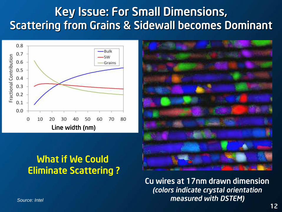
Key Issue: For Small Dimensions, Scattering from Grains & Sidewall becomes Dominant
Line width (nm)
What if We Could Eliminate Scattering ?
Cu wires at 17nm drawn dimension (colors indicate crystal orientation
measured with DSTEM) 12
Source: Intel
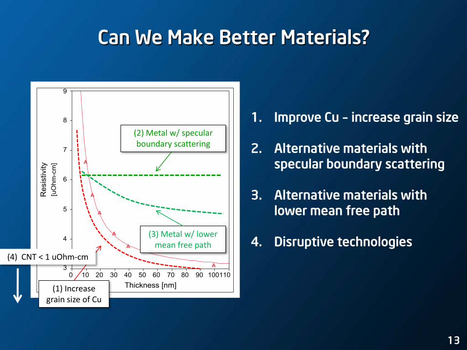
Can We Make Better Materials?
1. Improve Cu – increase grain size
2. Alternative materials with specular boundary scattering
3. Alternative materials with lower mean free path
4. Disruptive technologies
(2) Metal w/ specular boundary scattering
(3) Metal w/ lower mean free path
(1) Increase grain size of Cu
(4) CNT < 1 uOhm-cm
13
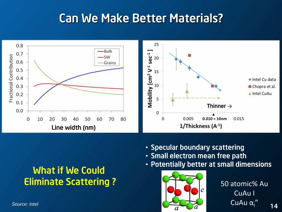
Can We Make Better Materials?
Line width (nm)
What if We Could Eliminate Scattering ?
• Specular boundary scattering • Small electron mean free path • Potentially better at small dimensions
50 atomic% Au CuAu I
CuAu αI”
0.010 = 10nm
Thinner →
14 Source: Intel
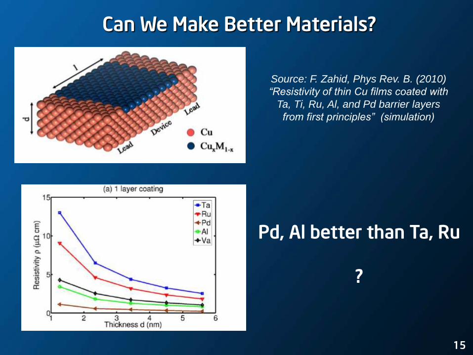
Can We Make Better Materials?
Source: F. Zahid, Phys Rev. B. (2010)
“Resistivity of thin Cu films coated with
Ta, Ti, Ru, Al, and Pd barrier layers
from first principles” (simulation)
Pd, Al better than Ta, Ru ?
15
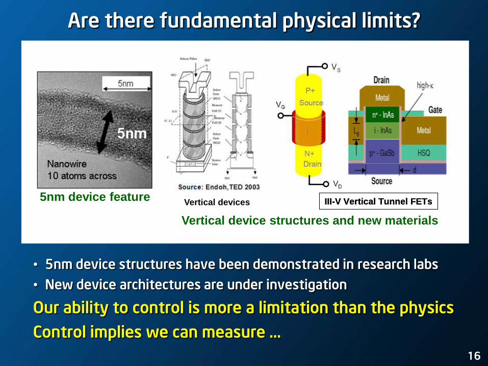
5nm device feature
Vertical device structures and new materials
Vertical devices III-V Vertical Tunnel FETsIII-V Vertical Tunnel FETs
Are there fundamental physical limits?
• 5nm device structures have been demonstrated in research labs
• New device architectures are under investigation
Our ability to control is more a limitation than the physics
Control implies we can measure …
16
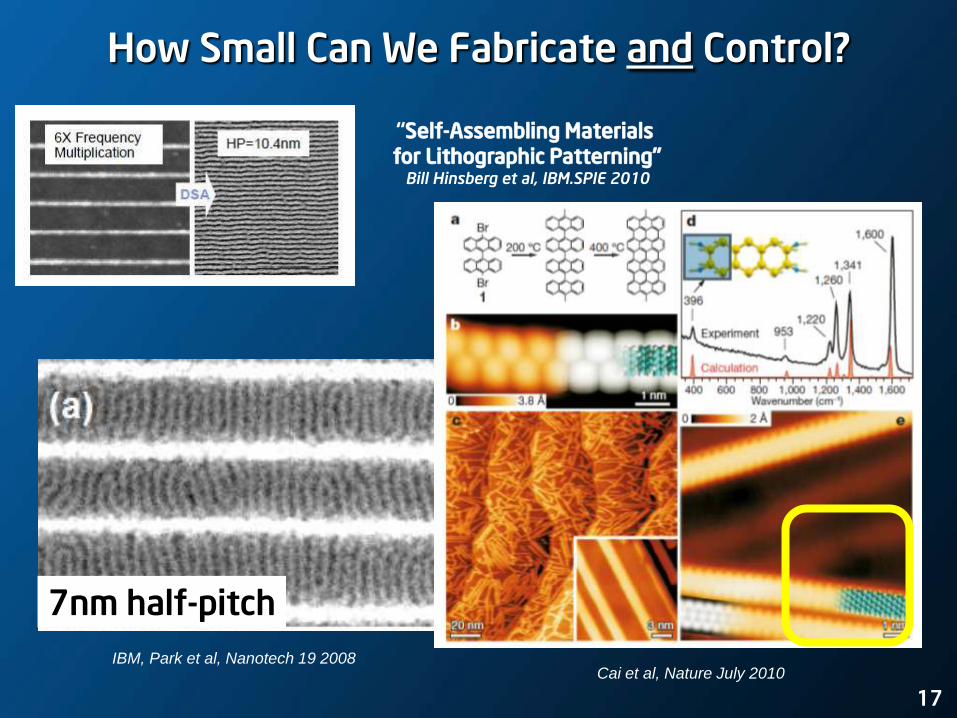
How Small Can We Fabricate and Control?
“Self-Assembling Materials for Lithographic Patterning”
Bill Hinsberg et al, IBM.SPIE 2010
7nm half-pitch
IBM, Park et al, Nanotech 19 2008 Cai et al, Nature July 2010
17
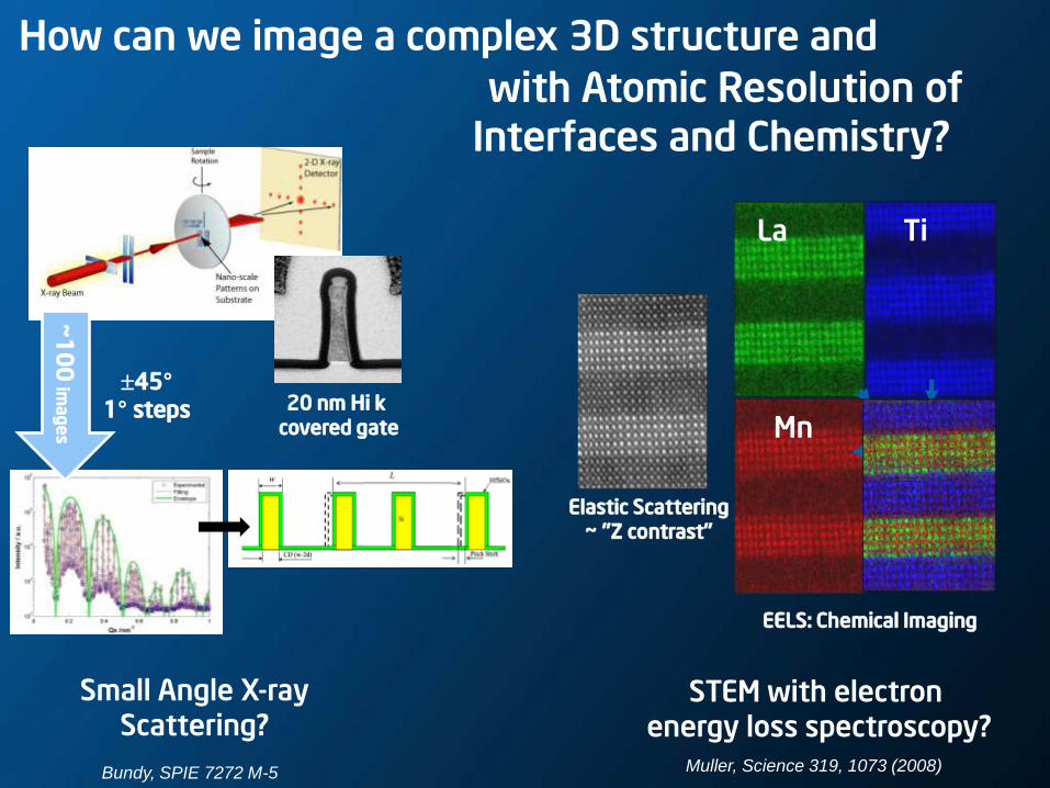
How can we image a complex 3D structure and
Small Angle X-ray Scattering?
~1
00
ima
ge
s
45° 1° steps 20 nm Hi k
covered gate
Bundy, SPIE 7272 M-5
with Atomic Resolution of Interfaces and Chemistry?
STEM with electron energy loss spectroscopy?
Elastic Scattering ~ "Z contrast"
Muller, Science 319, 1073 (2008)
EELS: Chemical Imaging
Mn
Ti La
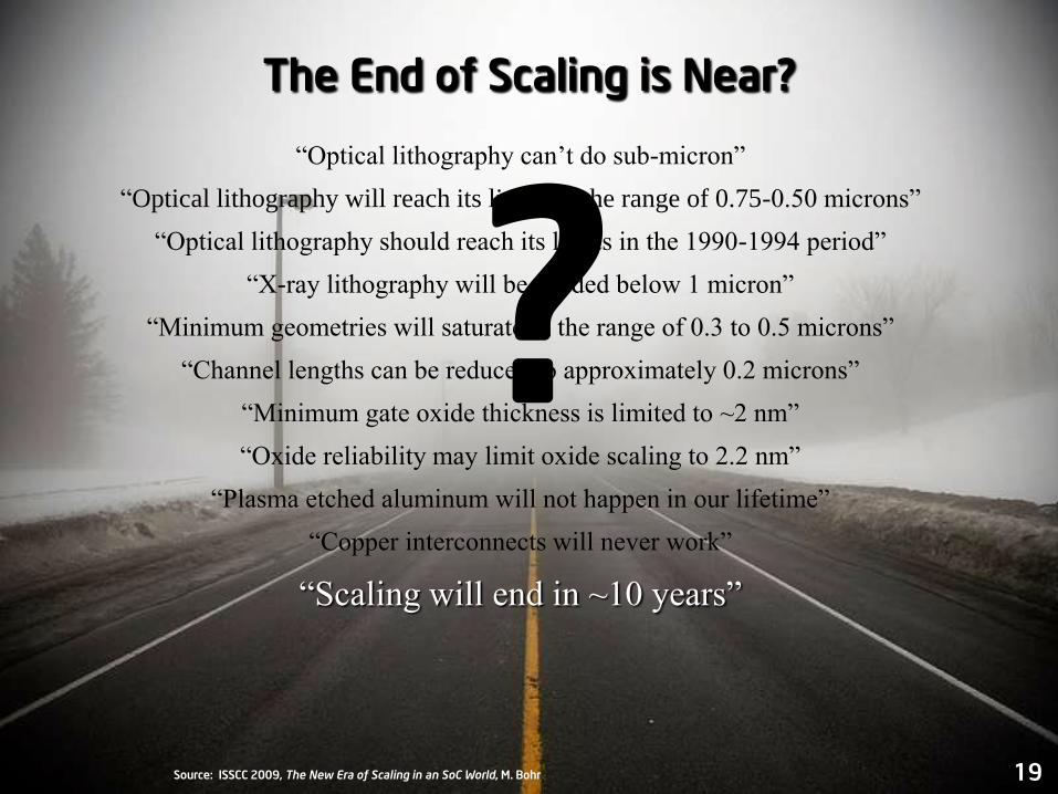
The End of Scaling is Near?
“Optical lithography can’t do sub-micron”
“Optical lithography will reach its limits in the range of 0.75-0.50 microns”
“Optical lithography should reach its limits in the 1990-1994 period”
“X-ray lithography will be needed below 1 micron”
“Minimum geometries will saturate in the range of 0.3 to 0.5 microns”
“Channel lengths can be reduced to approximately 0.2 microns”
“Minimum gate oxide thickness is limited to ~2 nm”
“Oxide reliability may limit oxide scaling to 2.2 nm”
“Plasma etched aluminum will not happen in our lifetime”
“Copper interconnects will never work”
“Scaling will end in ~10 years”
Source: ISSCC 2009, The New Era of Scaling in an SoC World, M. Bohr 19
?
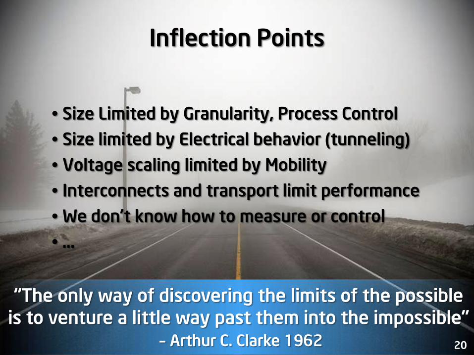
Inflection Points
Size Limited by Granularity, Process Control
Size limited by Electrical behavior (tunneling)
Voltage scaling limited by Mobility
Interconnects and transport limit performance
We don’t know how to measure or control
…
“The only way of discovering the limits of the possible is to venture a little way past them into the impossible”
– Arthur C. Clarke 1962 20
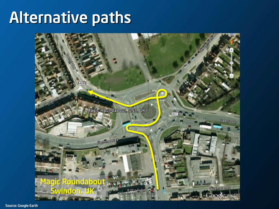
Alternative paths
Source: Google Earth
Magic Roundabout Swindon, UK
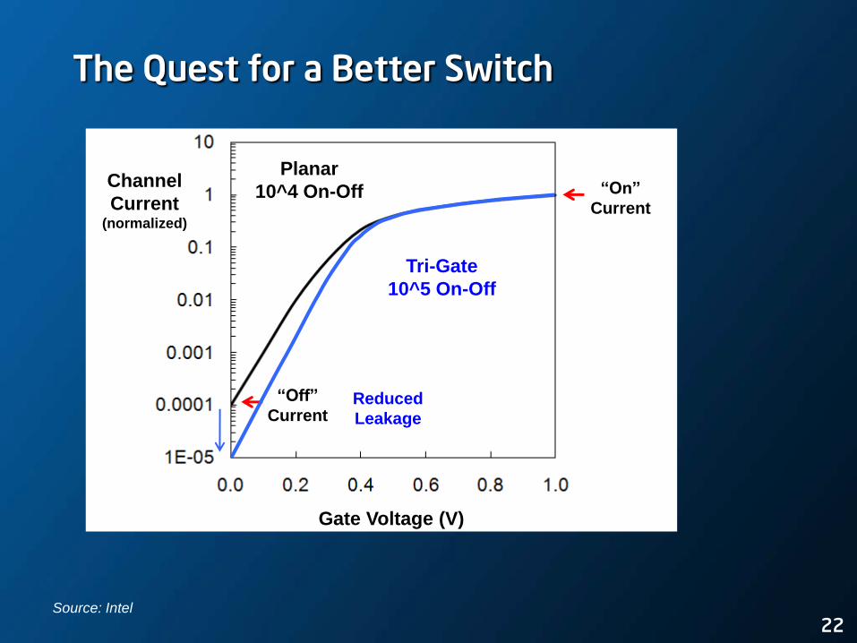
The Quest for a Better Switch
Gate Voltage (V)
“On”
Current
“Off”
Current
Channel
Current (normalized)
Planar
10^4 On-Off
Tri-Gate
10^5 On-Off
Reduced
Leakage
22 Source: Intel
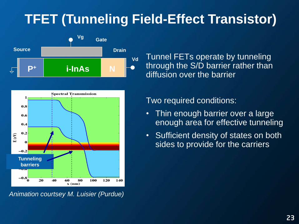
Vd
P+ i-InAs N
Vg
TFET (Tunneling Field-Effect Transistor)
Gate
Source Drain
Tunneling
barriers
Animation courtsey M. Luisier (Purdue)
Tunnel FETs operate by tunneling through the S/D barrier rather than diffusion over the barrier
Two required conditions:
• Thin enough barrier over a large enough area for effective tunneling
• Sufficient density of states on both sides to provide for the carriers
23
11
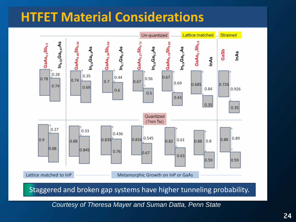
HTFET Material Considerations
Lattice matched to InP Metamorphic Growth on InP or GaAs
Staggered and broken gap systems have higher tunneling probability.
Courtesy of Theresa Mayer and Suman Datta, Penn State
24
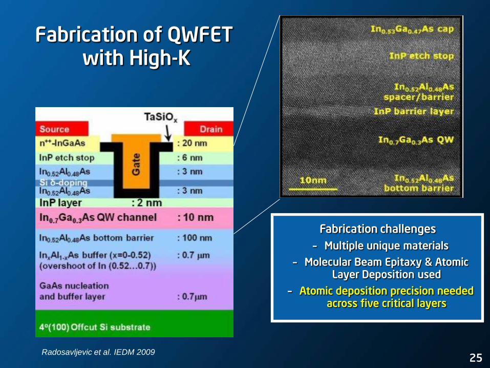
Fabrication of QWFET with High-K
Fabrication challenges
– Multiple unique materials
– Molecular Beam Epitaxy & Atomic Layer Deposition used
– Atomic deposition precision needed across five critical layers
25 Radosavljevic et al. IEDM 2009

Fabrication challenges
– Multiple unique materials
– Molecular Beam Epitaxy & Atomic Layer Deposition used
– Atomic deposition precision needed across multiple critical layers
– Complex band edge engineering in 3D
Fabrication of TFET
26
What we can make What we
need to make
Radosavljevic et al. IEDM 2009 Dewey et al. IEDM 2011

Rethinking Interconnects
Shrink Pitch To add more wires
Stack Layers To add more wires
Stack Layers Above and below To add more wires And more devices
Tinker with materials
27
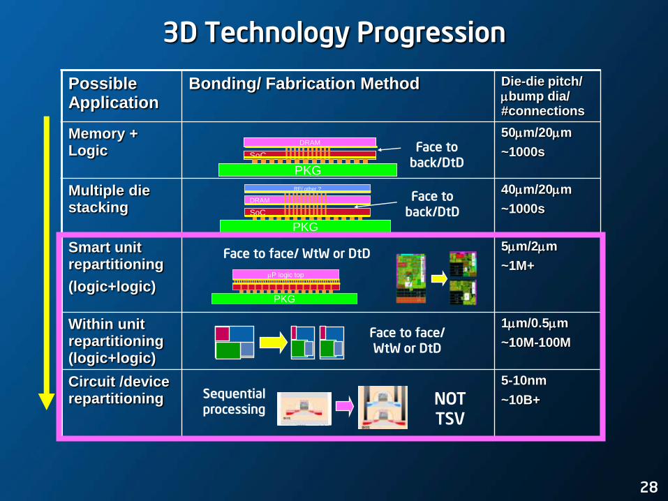
Possible Application
Bonding/ Fabrication Method Die-die pitch/ mbump dia/ #connections
Memory + Logic
50mm/20mm
~1000s
Multiple die stacking
40mm/20mm
~1000s
Smart unit repartitioning
(logic+logic)
5mm/2mm
~1M+
Within unit repartitioning (logic+logic)
1mm/0.5mm
~10M-100M
Circuit /device repartitioning
5-10nm
~10B+
3D Technology Progression
Face to back/DtD
SoC
PKG
DRAM
SoC
PKG
DRAM
SoC
PKG
DRAM
PKG
mP logic top
Face to face/ WtW or DtD
SoC
PKG
DRAM
RF/ other ?
Face to back/DtD
Face to face/ WtW or DtD
Sequential processing
NOT TSV
28
Stacked Latch
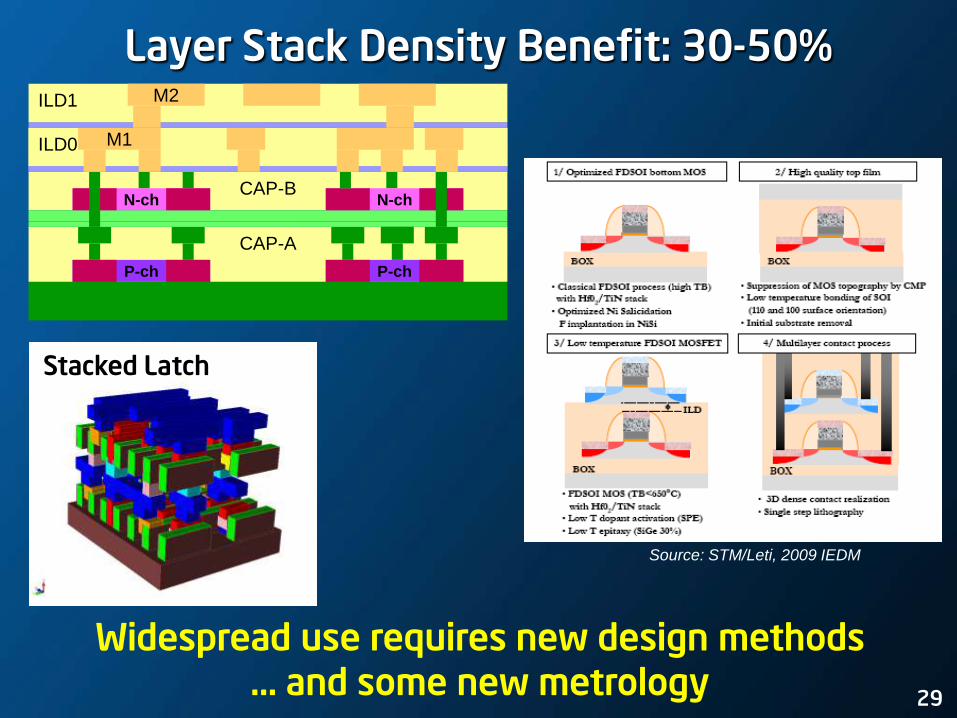
Layer Stack Density Benefit: 30-50%
Source: STM/Leti, 2009 IEDM
CAP-B
CAP-A
P-ch P-ch
N-ch N-ch
ILD0 ILD0 M1
ILD1 M2
Widespread use requires new design methods … and some new metrology
29

Heterogeneous System Integration
Logic
Memory
Power Reg.
Radio
Sensors
Photonics
2-D Integration (SoC)
3-D Integration (SiP)
Future systems will integrate a much wider
variety of materials and device structures
Source: IEDM 2011: The Evolution of Scaling from the Homogeneous Era to the Heterogeneous Era, M. Bohr
Pushing beyond the frontier
Source: M. Mayberry
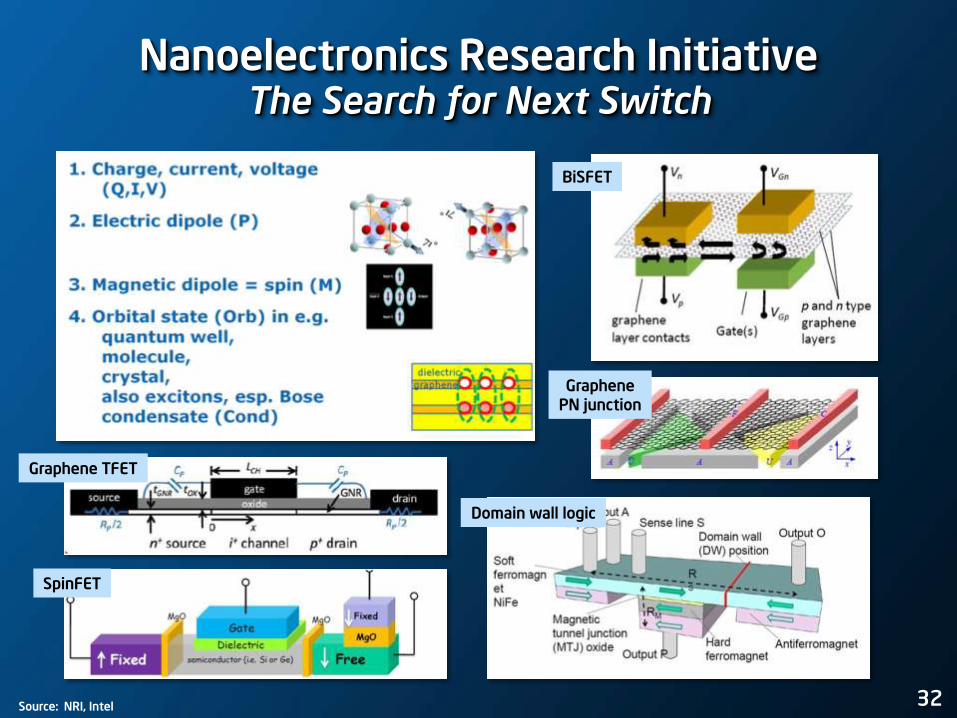
Nanoelectronics Research Initiative The Search for Next Switch
BiSFET
Graphene PN junction
SpinFET
Graphene TFET
Domain wall logic
Source: NRI, Intel 32
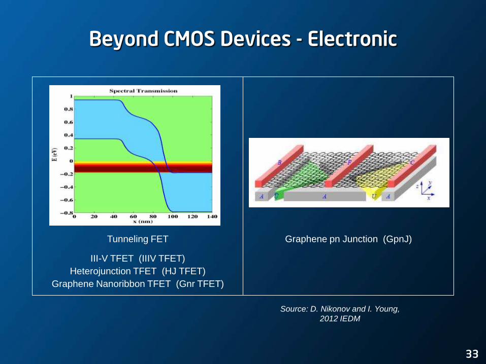
Beyond CMOS Devices - Electronic
Tunneling FET
III-V TFET (IIIV TFET)
Heterojunction TFET (HJ TFET)
Graphene Nanoribbon TFET (Gnr TFET)
Graphene pn Junction (GpnJ)
Source: D. Nikonov and I. Young,
2012 IEDM
33
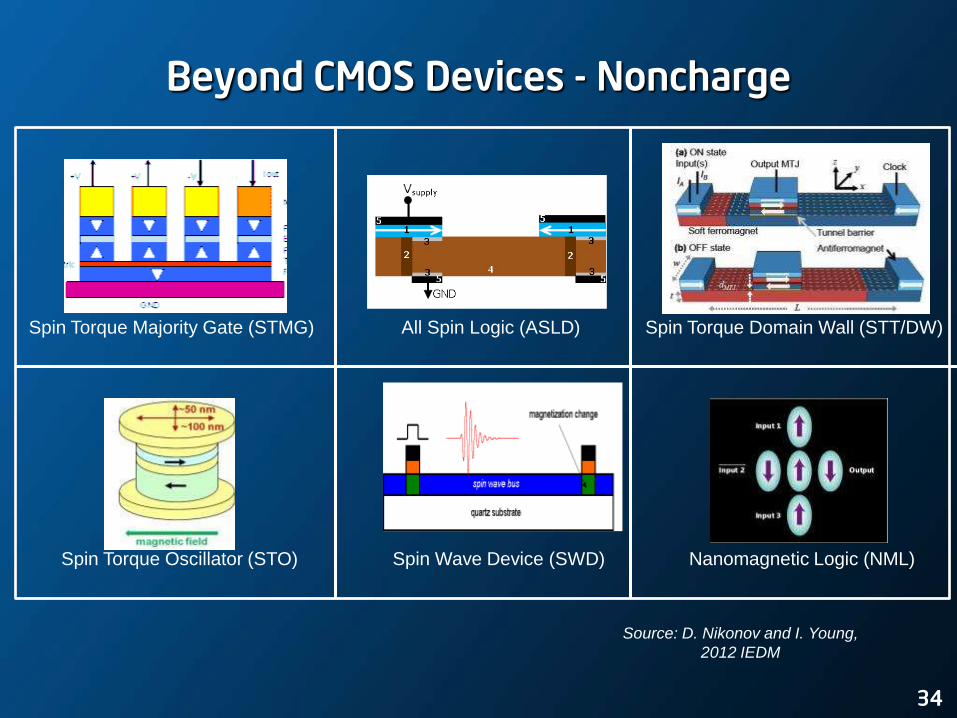
Beyond CMOS Devices - Noncharge
All Spin Logic (ASLD)
Spin Wave Device (SWD) Nanomagnetic Logic (NML)
Spin Torque Majority Gate (STMG)
Spin Torque Oscillator (STO)
Source: D. Nikonov and I. Young,
2012 IEDM
Spin Torque Domain Wall (STT/DW)
34
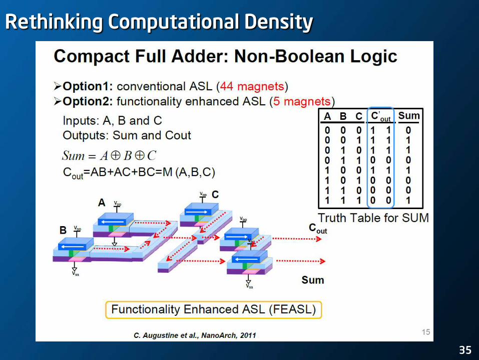
Rethinking Computational Density
35
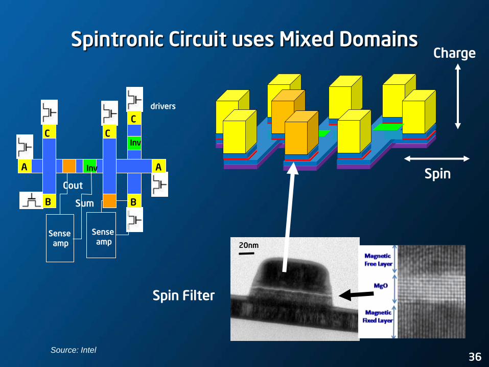
Spintronic Circuit uses Mixed Domains
drivers
A
B
Inv
C
C
Inv
C
B
A
Cout
Sum
Sense amp
Sense amp
36
20nm
Charge
Spin
Spin Filter
Source: Intel
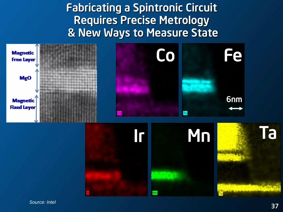
Fabricating a Spintronic Circuit Requires Precise Metrology
& New Ways to Measure State
Fe Co
Ta Ir Mn
6nm
37 Source: Intel
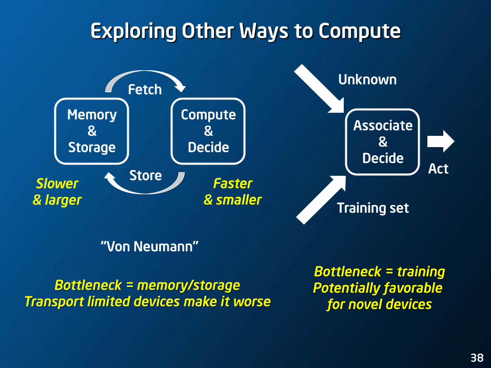
Exploring Other Ways to Compute
Memory &
Storage
Fetch
Store Slower & larger
Faster & smaller
“Von Neumann”
Bottleneck = memory/storage Transport limited devices make it worse
Compute &
Decide
Associate &
Decide
Training set
Unknown
Act
Bottleneck = training Potentially favorable
for novel devices
38
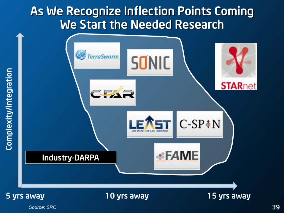
As We Recognize Inflection Points Coming We Start the Needed Research
5 yrs away 10 yrs away 15 yrs away
Co
mp
lex
ity
/in
teg
rati
on
Industry-DARPA
39 Source: SRC
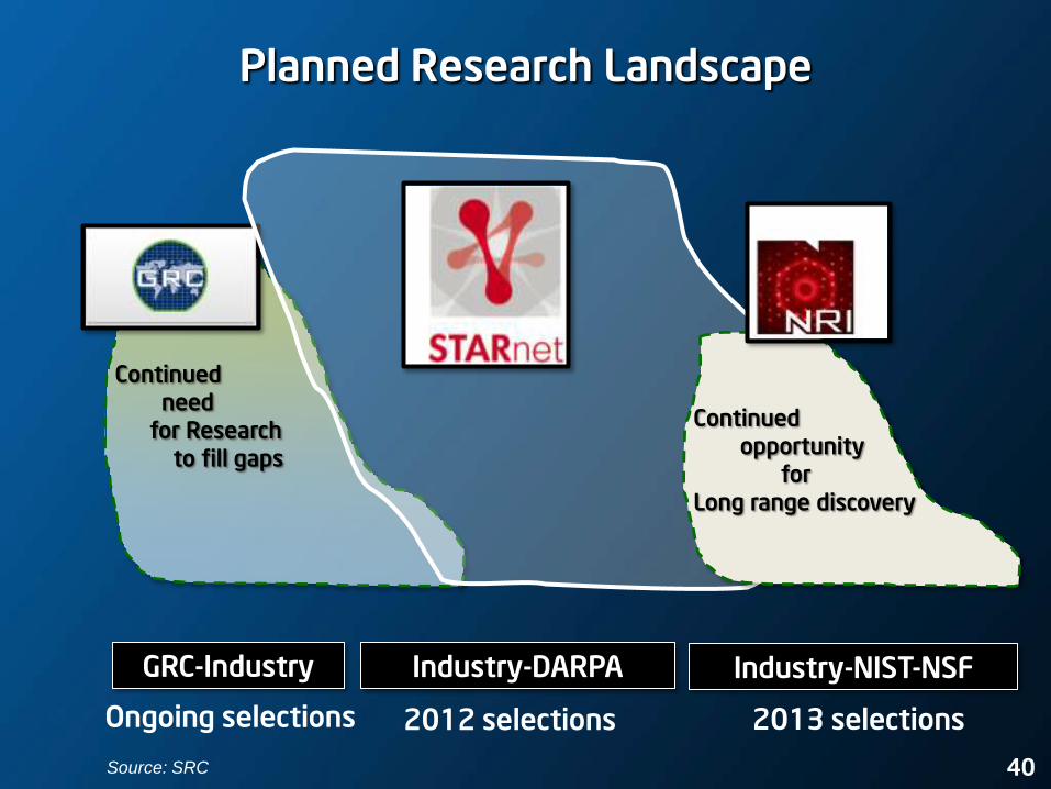
Continued need for Research to fill gaps
Planned Research Landscape
GRC-Industry
Continued opportunity for Long range discovery
Industry-NIST-NSF Industry-DARPA
Ongoing selections 2012 selections 2013 selections
40 Source: SRC
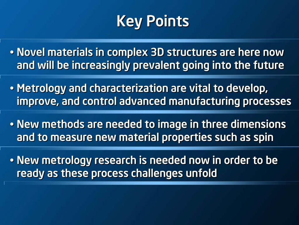
Key Points
Novel materials in complex 3D structures are here now and will be increasingly prevalent going into the future
Metrology and characterization are vital to develop, improve, and control advanced manufacturing processes
New methods are needed to image in three dimensions and to measure new material properties such as spin
New metrology research is needed now in order to be ready as these process challenges unfold

Thank You
Risk Factors The above statements and any others in this document that refer to plans and expectations for the first quarter, the year and the future are forward-looking statements that involve a number of risks and uncertainties. Words such as “anticipates,” “expects,” “intends,” “plans,” “believes,” “seeks,” “estimates,” “may,” “will,” “should” and their variations identify forward-looking statements. Statements that refer to or are based on projections, uncertain events or assumptions also identify forward-looking statements. Many factors could affect Intel’s actual results, and variances from Intel’s current expectations regarding such factors could cause actual results to differ materially from those expressed in these forward-looking statements. Intel presently considers the following to be the important factors that could cause actual results to differ materially from the company’s expectations. Demand could be different from Intel's expectations due to factors including changes in business and economic conditions, including supply constraints and other disruptions affecting customers; customer acceptance of Intel’s and competitors’ products; changes in customer order patterns including order cancellations; and changes in the level of inventory at customers. Uncertainty in global economic and financial conditions poses a risk that consumers and businesses may defer purchases in response to negative financial events, which could negatively affect product demand and other related matters. Intel operates in intensely competitive industries that are characterized by a high percentage of costs that are fixed or difficult to reduce in the short term and product demand that is highly variable and difficult to forecast. Revenue and the gross margin percentage are affected by the timing of Intel product introductions and the demand for and market acceptance of Intel's products; actions taken by Intel's competitors, including product offerings and introductions, marketing programs and pricing pressures and Intel’s response to such actions; and Intel’s ability to respond quickly to technological developments and to incorporate new features into its products. Intel is in the process of transitioning to its next generation of products on 22nm process technology, and there could be execution and timing issues associated with these changes, including products defects and errata and lower than anticipated manufacturing yields. The gross margin percentage could vary significantly from expectations based on capacity utilization; variations in inventory valuation, including variations related to the timing of qualifying products for sale; changes in revenue levels; product mix and pricing; the timing and execution of the manufacturing ramp and associated costs; start-up costs; excess or obsolete inventory; changes in unit costs; defects or disruptions in the supply of materials or resources; product manufacturing quality/yields; and impairments of long-lived assets, including manufacturing, assembly/test and intangible assets. The majority of Intel’s non-marketable equity investment portfolio balance is concentrated in companies in the flash memory market segment, and declines in this market segment or changes in management’s plans with respect to Intel’s investments in this market segment could result in significant impairment charges, impacting restructuring charges as well as gains/losses on equity investments and interest and other. Intel's results could be affected by adverse economic, social, political and physical/infrastructure conditions in countries where Intel, its customers or its suppliers operate, including military conflict and other security risks, natural disasters, infrastructure disruptions, health concerns and fluctuations in currency exchange rates. Expenses, particularly certain marketing and compensation expenses, as well as restructuring and asset impairment charges, vary depending on the level of demand for Intel's products and the level of revenue and profits. Intel’s results could be affected by the timing of closing of acquisitions and divestitures. Intel's results could be affected by adverse effects associated with product defects and errata (deviations from published specifications), and by litigation or regulatory matters involving intellectual property, stockholder, consumer, antitrust and other issues, such as the litigation and regulatory matters described in Intel's SEC reports. An unfavorable ruling could include monetary damages or an injunction prohibiting us from manufacturing or selling one or more products, precluding particular business practices, impacting Intel’s ability to design its products, or requiring other remedies such as compulsory licensing of intellectual property. A detailed discussion of these and other factors that could affect Intel’s results is included in Intel’s SEC filings, including the annual report on Form 10-K for the fiscal year ended December 31, 2012.