Embed Size (px)
Citation preview
1. General description
PTN36043 is a very small, low power 2 differential channel 2 to 1 active multiplex/demultiplexer switch with integrated SuperSpeed USB 3.1 Gen 1 (also known as USB 3.0) redriver IC that can switch two differential signals to one of two locations. The active switch has optimized performance with minimized crosstalk, as required by the high-speed serial interface for USB Type-C connector. PTN36043 allows expansion of existing high-speed ports for very low power consumption.
With integrated USB 3.1 Gen 1 redriver, signal quality is enhanced by performing receive equalization on the deteriorated input signal followed by transmit de-emphasis maximizing system link performance. With its superior differential signal conditioning and enhancement capability, the device delivers significant flexibility and performance scaling for various systems with different PCB characteristics and cable channel conditions and still benefit from optimum power consumption.
PTN36043 has built-in advanced power management capability that enables significant power savings under various different USB 3.1 Gen 1 Low-power modes (U2/U3). It can detect link electrical conditions and can dynamically activate/de-activate internal circuitry and logic. The device performs these actions without host software intervention and conserves power.
PTN36043 is powered from a 1.8 V supply and is available in a small DHX2QFN18 package (2.4 mm 2.0 mm 0.35 mm) with 0.4 mm pitch.
2. Features and benefits
2 bidirectional differential channel, 2 : 1 multiplex/demultiplexer switch, supports USB 3.1 Gen 1 specification (SuperSpeed only)
Compliant to SuperSpeed USB 3.1 Gen 1 standard
Pin out data flow matches USB Type-C connector pin assignments
Two control pins for each channel to select optimized signal conditions
Receive equalization on each channel to recover from InterSymbol Interference (ISI) and high-frequency losses, with provision to choose equalization gain settings per channel
Transmit de-emphasis on each channel delivers pre-compensation suited to channel conditions
Output swing adjustment
Integrated termination resistors provide impedance matching on both transmit and receive sides
Automatic receiver termination detection
Low active power: 203 mW/113 mA (typical) for VDD = 1.8 V
PTN36043USB Type-C SuperSpeed active switchRev. 2 — 19 February 2018 Product data sheet
NXP Semiconductors PTN36043USB Type-C SuperSpeed active switch
Power-saving states:
1.35 mW/0.75 mA (typical) when in U2/U3 states
0.81 mW/0.45 mA (typical) when no connection detected
Excellent differential and common return loss performance
14 dB differential and 15 dB common-mode return loss for 10 MHz to 1250 MHz
Flow-through pinout to ease PCB layout and minimize crosstalk effects
Power supply: VDD = 1.8 V (typical)
Compliant with JESD 78 Class II latch up test standard
Very thin DHX2QFN18 package: 2.4 mm x 2.0 mm x 0.35 mm, 0.4 mm pitch
ESD protection exceeds 7000 V HBM per JDS-001-2012 and 1000 V CDM per JESD22-C101
Latch-up testing is done to JEDEC Standard JESD78 which exceeds 100 mA
Operating temperature range: 40°C to +85°C
3. Applications
USB 3.1 Gen 1 application for USB Type-C connectors
Smart Phones, Tablets/Mobile Devices
Desktop/Notebook Computers
Docking Stations
USB 3.1 Gen 1 Peripherals such as flat panel display, consumer/storage devices, printers or USB 3.1 Gen 1 capable hubs/repeaters
4. Ordering information
4.1 Ordering options
Table 1. Ordering information
Type number Topside marking
Package
Name Description Version
PTN36043BX 43 DHX2QFN18 plastic dual in-line compatible thermal enhanced extremely thin quad flat package; no leads; 18 terminals; body 2.4 mm 2.0 mm 0.35 mm
SOT1442-1
Table 2. Ordering options
Type number Orderable part number
Package Packing method Minimum order quantity
Temperature
PTN36043BX PTN36043BXY DHX2QFN18 REEL 13" Q1/T1 *STANDARD MARK SMD DP
10000 Tamb = 40 C to +85 C
PTN36043 All information provided in this document is subject to legal disclaimers. © NXP Semiconductors N.V. 2018. All rights reserved.
Product data sheet Rev. 2 — 19 February 2018 2 of 29
NXP Semiconductors PTN36043USB Type-C SuperSpeed active switch
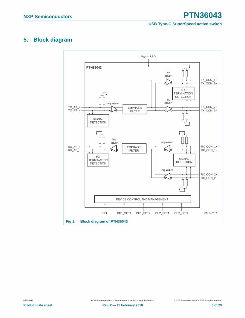
5. Block diagram
Fig 1. Block diagram of PTN36043
aaa-017471
PTN36043
VDD = 1.8 V
EMPHASISFILTER
DEVICE CONTROL AND MANAGEMENT
SIGNALDETECTION
RX_AP_+RX_AP_−
TX_AP_+
TX_CON_1+TX_CON_1−
TX_CON_2+TX_CON_2−
RX_CON_1+RX_CON_1−
RX_CON_2+RX_CON_2−
TX_AP_−
EMPHASISFILTER
SEL CH1_SET1 CH1_SET2 CH2_SET1 CH2_SET2
equalizer
SIGNALDETECTION
linedriver equalizer
RXTERMINATIONDETECTION
linedriver
RXTERMINATIONDETECTION
linedriver
equalizer
PTN36043 All information provided in this document is subject to legal disclaimers. © NXP Semiconductors N.V. 2018. All rights reserved.
Product data sheet Rev. 2 — 19 February 2018 3 of 29
NXP Semiconductors PTN36043USB Type-C SuperSpeed active switch
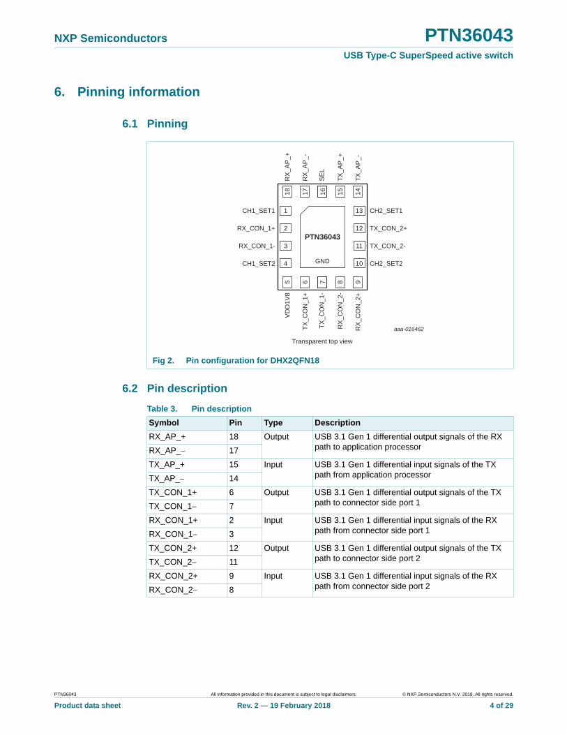
6. Pinning information
6.1 Pinning
6.2 Pin description
Fig 2. Pin configuration for DHX2QFN18
aaa-016462
GND
16 15 14TX
_AP
_-
1718
SE
L
PTN36043
4
3
2
1
CH1_SET2
RX_CON_1-
RX_CON_1+
CH1_SET1
10
11
12
13
CH2_SET2
TX_CON_2-
TX_CON_2+
CH2_SET1
TX_A
P_+
RX
_AP
_-
RX
_AP
_+
RX
_CO
N_2
+
TX_C
ON
_1-
RX
_CO
N_2
-
TX_C
ON
_1+
VD
D1V
8
7 8 965
Transparent top view
Table 3. Pin description
Symbol Pin Type Description
RX_AP_+ 18 Output USB 3.1 Gen 1 differential output signals of the RX path to application processorRX_AP_ 17
TX_AP_+ 15 Input USB 3.1 Gen 1 differential input signals of the TX path from application processorTX_AP_ 14
TX_CON_1+ 6 Output USB 3.1 Gen 1 differential output signals of the TX path to connector side port 1TX_CON_1 7
RX_CON_1+ 2 Input USB 3.1 Gen 1 differential input signals of the RX path from connector side port 1RX_CON_1 3
TX_CON_2+ 12 Output USB 3.1 Gen 1 differential output signals of the TX path to connector side port 2TX_CON_2 11
RX_CON_2+ 9 Input USB 3.1 Gen 1 differential input signals of the RX path from connector side port 2RX_CON_2 8
PTN36043 All information provided in this document is subject to legal disclaimers. © NXP Semiconductors N.V. 2018. All rights reserved.
Product data sheet Rev. 2 — 19 February 2018 4 of 29
NXP Semiconductors PTN36043USB Type-C SuperSpeed active switch
SEL 16 input Output selection control
When SEL=0, RX_AP_/TX_AP_ are connected to RX_CON_2/TX_CON_2, and RX_CON_1/TX_CON_1 are connected to VDD thru low ohmic resistor (50 ).
When SEL=1, RX_AP_/TX_AP_ are connected to RX_CON_1/TX_CON_1, and RX_CON_2/TX_CON_2 are connected to VDD thru low ohmic resistor (50 ).
CH1_SET1 1 Ternary input
OS/DE/EQ control pins for channel facing the application processor sideCH1_SET2 4
CH2_SET1 13 Ternary input
OS/DE/EQ control pins for channel facing the connector sideCH2_SET2 10
VDD1V8 5 Power Power supply (1.8 V typical)
GND Center Pad
Power Ground. Center pad must be connected to GND plane for both electrical grounding and thermal relief purposes.
Table 3. Pin description …continued
Symbol Pin Type Description
PTN36043 All information provided in this document is subject to legal disclaimers. © NXP Semiconductors N.V. 2018. All rights reserved.
Product data sheet Rev. 2 — 19 February 2018 5 of 29
NXP Semiconductors PTN36043USB Type-C SuperSpeed active switch
7. Functional description
Refer to Figure 1 “Block diagram of PTN36043”.
PTN36043 is a high speed 2 to 1 active switch with integrated SuperSpeed USB 3.1 Gen 1 redriver meant to be used for signal integrity enhancement on various platforms - smart phone, tablet, notebook, hub, A/V display and peripheral devices, for example. With its high fidelity differential signal conditioning capability and wide configurability, this device is flexible and versatile enough for use under a variety of system environments.
The following sections describe the individual block functions and capabilities of the device in more detail.
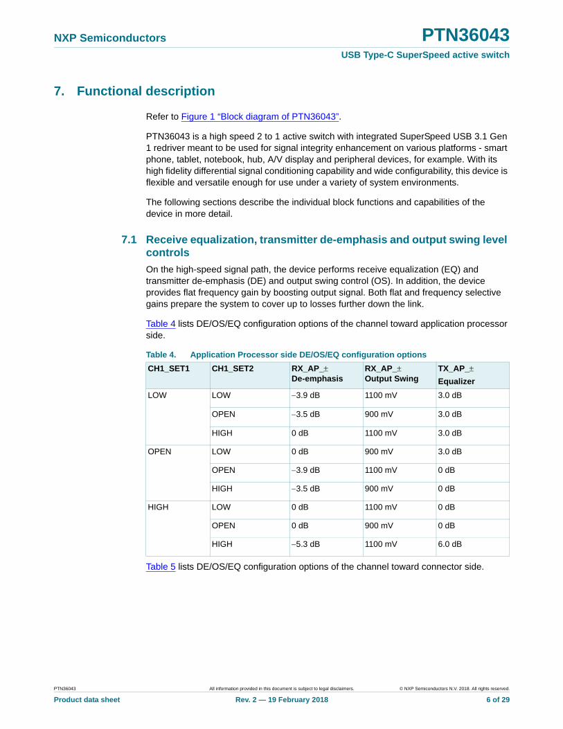
7.1 Receive equalization, transmitter de-emphasis and output swing level controls
On the high-speed signal path, the device performs receive equalization (EQ) and transmitter de-emphasis (DE) and output swing control (OS). In addition, the device provides flat frequency gain by boosting output signal. Both flat and frequency selective gains prepare the system to cover up to losses further down the link.
Table 4 lists DE/OS/EQ configuration options of the channel toward application processor side.
Table 5 lists DE/OS/EQ configuration options of the channel toward connector side.
Table 4. Application Processor side DE/OS/EQ configuration options
CH1_SET1 CH1_SET2 RX_AP_ De-emphasis
RX_AP_ Output Swing
TX_AP_
Equalizer
LOW LOW 3.9 dB 1100 mV 3.0 dB
OPEN 3.5 dB 900 mV 3.0 dB
HIGH 0 dB 1100 mV 3.0 dB
OPEN LOW 0 dB 900 mV 3.0 dB
OPEN 3.9 dB 1100 mV 0 dB
HIGH 3.5 dB 900 mV 0 dB
HIGH LOW 0 dB 1100 mV 0 dB
OPEN 0 dB 900 mV 0 dB
HIGH 5.3 dB 1100 mV 6.0 dB
PTN36043 All information provided in this document is subject to legal disclaimers. © NXP Semiconductors N.V. 2018. All rights reserved.
Product data sheet Rev. 2 — 19 February 2018 6 of 29
NXP Semiconductors PTN36043USB Type-C SuperSpeed active switch
7.2 Device states and power management
PTN36043 has implemented an advanced power management scheme that operates in tune with USB 3.1 Gen 1 bus electrical condition. Although the device does not decode USB power management commands (related to USB 3.1 Gen 1 U1/U2/U3 transitions) exchanged between USB 3.1 Gen 1 host and peripheral/device, it relies on bus electrical conditions and SEL pin setting to decide to be in one of the following states:
• Active state wherein device is fully operational, USB data is transported on either port 1 or port 2 in Figure 1. In this state, USB connection exists and the Receive Termination indication remains active. But there is no need for Receive Termination detection.
• Power-saving state wherein either port 1 or port 2 is kept enabled. In this state, squelching, detection and/or Receive termination detection circuitry are active. Based on USB connection, there are two possibilities:
– No USB connection.
– A USB connection exists and the link is in USB 3.1 Gen 1 U2/U3 mode.
• Off state when PTN36043 is not being powered (i.e., VDD1V8 = 0 V), special steps should be done to prevent back-current issues on control pins such SEL or CH1/2_SET1/2 pins when these pins' states are not low. These pins can be controlled through two different ways.
– pull-up/pull-down resistors - make sure these pull-up resistors' VDD is the same power source as to power PTN36043. When power to PTN36043 is off, power to these pull-up resistors will be off as well.
– external processor's GPIO - if PTN36043 is turned off when the external processor's power stays on, processor should configure these GPIOs connected to these control pins as output low (< 0.4 V) or tri-state mode (configure GPIOs as input mode). This will make sure no current will be flowing into PTN36043 through these control pins.
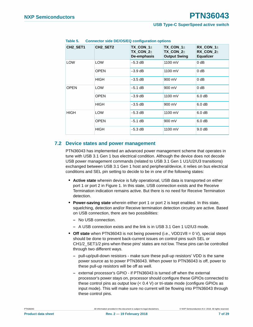
Table 5. Connector side DE/OS/EQ configuration options
CH2_SET1 CH2_SET2 TX_CON_1 TX_CON_2De-emphasis
TX_CON_1 TX_CON_2 Output Swing
RX_CON_1RX_CON_2Equalizer
LOW LOW 5.3 dB 1100 mV 0 dB
OPEN 3.9 dB 1100 mV 0 dB
HIGH 3.5 dB 900 mV 0 dB
OPEN LOW 5.1 dB 900 mV 0 dB
OPEN 3.9 dB 1100 mV 6.0 dB
HIGH 3.5 dB 900 mV 6.0 dB
HIGH LOW 5.3 dB 1100 mV 6.0 dB
OPEN 5.1 dB 900 mV 6.0 dB
HIGH 5.3 dB 1100 mV 9.0 dB
PTN36043 All information provided in this document is subject to legal disclaimers. © NXP Semiconductors N.V. 2018. All rights reserved.
Product data sheet Rev. 2 — 19 February 2018 7 of 29
NXP Semiconductors PTN36043USB Type-C SuperSpeed active switch
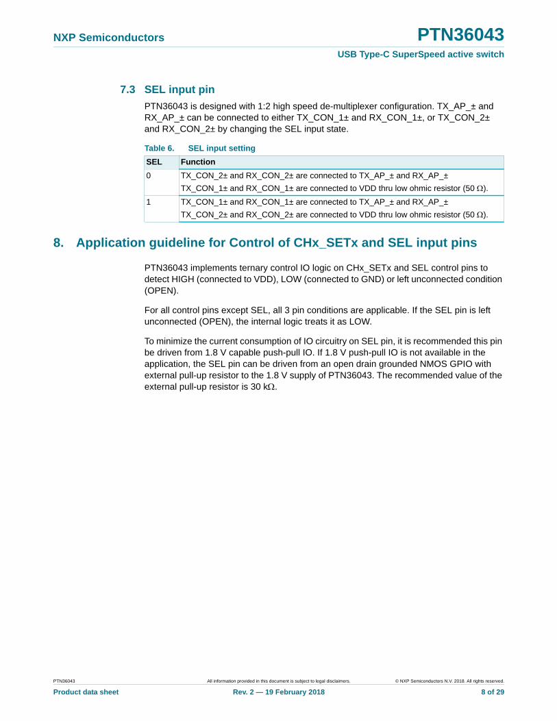
7.3 SEL input pin
PTN36043 is designed with 1:2 high speed de-multiplexer configuration. TX_AP_± and RX_AP_± can be connected to either TX_CON_1± and RX_CON_1±, or TX_CON_2± and RX_CON_2± by changing the SEL input state.
8. Application guideline for Control of CHx_SETx and SEL input pins
PTN36043 implements ternary control IO logic on CHx_SETx and SEL control pins to detect HIGH (connected to VDD), LOW (connected to GND) or left unconnected condition (OPEN).
For all control pins except SEL, all 3 pin conditions are applicable. If the SEL pin is left unconnected (OPEN), the internal logic treats it as LOW.
To minimize the current consumption of IO circuitry on SEL pin, it is recommended this pin be driven from 1.8 V capable push-pull IO. If 1.8 V push-pull IO is not available in the application, the SEL pin can be driven from an open drain grounded NMOS GPIO with external pull-up resistor to the 1.8 V supply of PTN36043. The recommended value of the external pull-up resistor is 30 k.
Table 6. SEL input setting
SEL Function
0 TX_CON_2± and RX_CON_2± are connected to TX_AP_± and RX_AP_±
TX_CON_1± and RX_CON_1± are connected to VDD thru low ohmic resistor (50 ).
1 TX_CON_1± and RX_CON_1± are connected to TX_AP_± and RX_AP_±
TX_CON_2± and RX_CON_2± are connected to VDD thru low ohmic resistor (50 ).
PTN36043 All information provided in this document is subject to legal disclaimers. © NXP Semiconductors N.V. 2018. All rights reserved.
Product data sheet Rev. 2 — 19 February 2018 8 of 29
NXP Semiconductors PTN36043USB Type-C SuperSpeed active switch
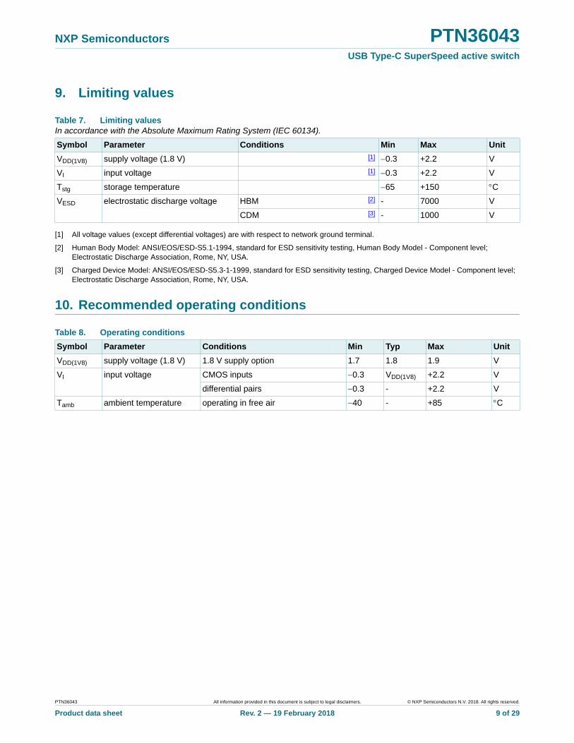
9. Limiting values
[1] All voltage values (except differential voltages) are with respect to network ground terminal.
[2] Human Body Model: ANSI/EOS/ESD-S5.1-1994, standard for ESD sensitivity testing, Human Body Model - Component level; Electrostatic Discharge Association, Rome, NY, USA.
[3] Charged Device Model: ANSI/EOS/ESD-S5.3-1-1999, standard for ESD sensitivity testing, Charged Device Model - Component level; Electrostatic Discharge Association, Rome, NY, USA.
10. Recommended operating conditions
Table 7. Limiting values In accordance with the Absolute Maximum Rating System (IEC 60134).
Symbol Parameter Conditions Min Max Unit
VDD(1V8) supply voltage (1.8 V) [1] 0.3 +2.2 V
VI input voltage [1] 0.3 +2.2 V
Tstg storage temperature 65 +150 C
VESD electrostatic discharge voltage HBM [2] - 7000 V
CDM [3] - 1000 V
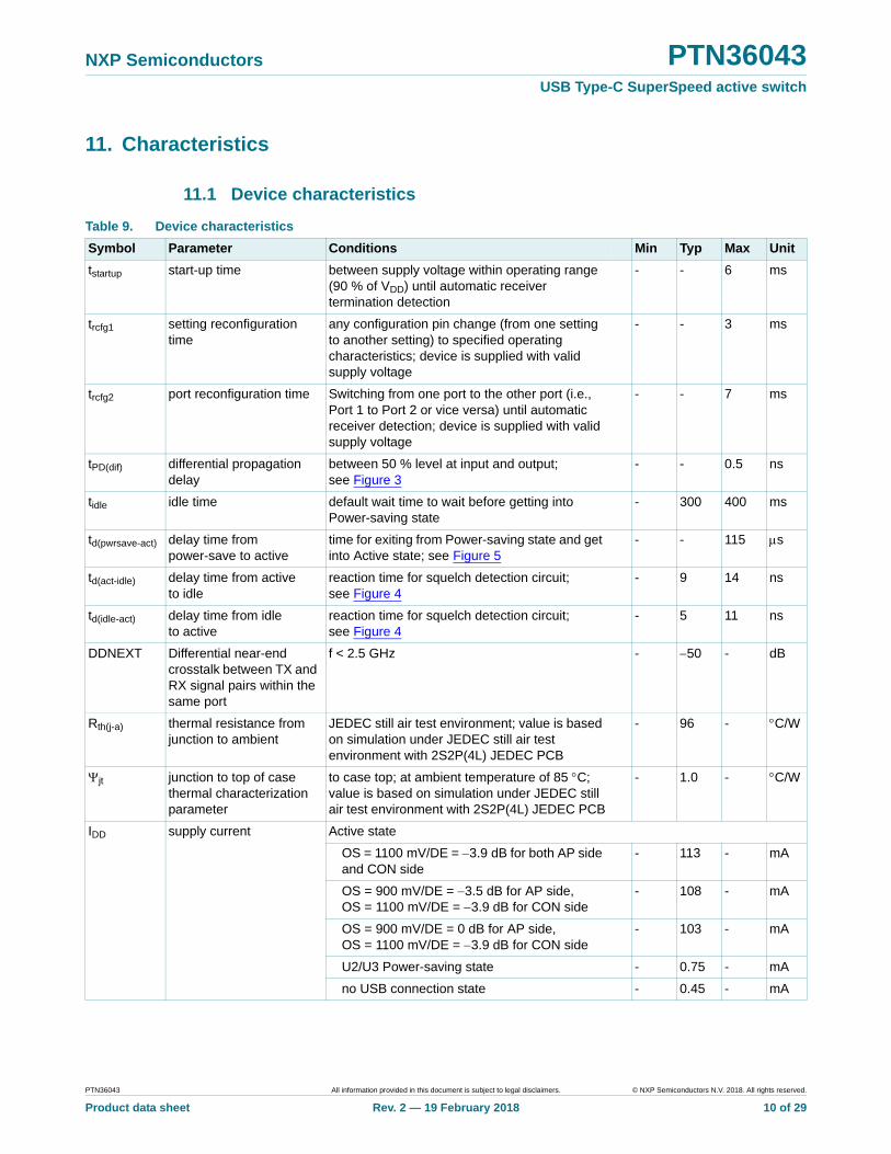
Table 8. Operating conditions
Symbol Parameter Conditions Min Typ Max Unit
VDD(1V8) supply voltage (1.8 V) 1.8 V supply option 1.7 1.8 1.9 V
VI input voltage CMOS inputs 0.3 VDD(1V8) +2.2 V
differential pairs 0.3 - +2.2 V
Tamb ambient temperature operating in free air 40 - +85 C
PTN36043 All information provided in this document is subject to legal disclaimers. © NXP Semiconductors N.V. 2018. All rights reserved.
Product data sheet Rev. 2 — 19 February 2018 9 of 29
NXP Semiconductors PTN36043USB Type-C SuperSpeed active switch
11. Characteristics
11.1 Device characteristics
Table 9. Device characteristics
Symbol Parameter Conditions Min Typ Max Unit
tstartup start-up time between supply voltage within operating range (90 % of VDD) until automatic receiver termination detection
- - 6 ms
trcfg1 setting reconfiguration time
any configuration pin change (from one setting to another setting) to specified operating characteristics; device is supplied with valid supply voltage
- - 3 ms
trcfg2 port reconfiguration time Switching from one port to the other port (i.e., Port 1 to Port 2 or vice versa) until automatic receiver detection; device is supplied with valid supply voltage
- - 7 ms
tPD(dif) differential propagation delay
between 50 % level at input and output; see Figure 3
- - 0.5 ns
tidle idle time default wait time to wait before getting into Power-saving state
- 300 400 ms
td(pwrsave-act) delay time from power-save to active
time for exiting from Power-saving state and get into Active state; see Figure 5
- - 115 s
td(act-idle) delay time from active to idle
reaction time for squelch detection circuit; see Figure 4
- 9 14 ns
td(idle-act) delay time from idle to active
reaction time for squelch detection circuit; see Figure 4
- 5 11 ns
DDNEXT Differential near-end crosstalk between TX and RX signal pairs within the same port
f < 2.5 GHz - 50 - dB
Rth(j-a) thermal resistance from junction to ambient
JEDEC still air test environment; value is based on simulation under JEDEC still air test environment with 2S2P(4L) JEDEC PCB
- 96 - C/W
jt junction to top of case thermal characterization parameter
to case top; at ambient temperature of 85 C; value is based on simulation under JEDEC still air test environment with 2S2P(4L) JEDEC PCB
- 1.0 - C/W
IDD supply current Active state
OS = 1100 mV/DE = 3.9 dB for both AP side and CON side
- 113 - mA
OS = 900 mV/DE = 3.5 dB for AP side, OS = 1100 mV/DE = 3.9 dB for CON side
- 108 - mA
OS = 900 mV/DE = 0 dB for AP side, OS = 1100 mV/DE = 3.9 dB for CON side
- 103 - mA
U2/U3 Power-saving state - 0.75 - mA
no USB connection state - 0.45 - mA
PTN36043 All information provided in this document is subject to legal disclaimers. © NXP Semiconductors N.V. 2018. All rights reserved.
Product data sheet Rev. 2 — 19 February 2018 10 of 29

NXP Semiconductors PTN36043USB Type-C SuperSpeed active switch
Fig 3. Propagation delay Fig 4. LFPS electrical idle transitions in U0/U1 modes
in
tPD(dif)
002aag025
out
tPD(dif) td(idle-act)
002aag026
VDC_CM
VDC_CM
td(act-idle)
IN+
IN−
OUT+
OUT−
VSQTH
Fig 5. U2/U3 exit behavior
channel A, RX
channel A, TX
channel B, RX
channel B, TX
block activetd(pwrsave-act)
002aag028
U2 exit LFPS
U2 exit LFPS
RECOVERY
RECOVERY
U2 exit handshake LFPS
U2 exit handshake LFPS
RECOVERY
RECOVERY
PTN36043 All information provided in this document is subject to legal disclaimers. © NXP Semiconductors N.V. 2018. All rights reserved.
Product data sheet Rev. 2 — 19 February 2018 11 of 29
NXP Semiconductors PTN36043USB Type-C SuperSpeed active switch
11.2 Receiver AC/DC characteristics
Table 10. Receiver AC/DC characteristics
Symbol Parameter Conditions Min Typ Max Unit
ZRX_DC receiver DC common-mode impedance 18 - 30
ZRX_DIFF_DC DC differential impedance RX pair 72 - 120
ZRX_HIGH_IMP common-mode input impedance DC common-mode input impedance when output of redriver is not terminated
25 - - k
VRX(diff)(p-p) peak-to-peak differential receiver voltage 100 - 1200 mV
VRX_DC_CM RX DC common mode voltage - 1.8 - V
VRX_CM_AC_P RX AC common-mode voltage peak - - 150 mV
Vth(i) signal detector input threshold voltage differential peak-to-peak value
75 - 150 mV
RLDD11,RX RX differential mode return loss 10 MHz to 1250 MHz 12 14 - dB
1250 MHz to 2500 MHz 7 8.5 - dB
2500 MHz to 3000 MHz 6 7.5 - dB
RLCC11,RX RX common mode return loss 10 MHz to 1250 MHz 12 15 - dB
1250 MHz to 2500 MHz 8 10 - dB
2500 MHz to 3000 MHz 7 9 - dB
PTN36043 All information provided in this document is subject to legal disclaimers. © NXP Semiconductors N.V. 2018. All rights reserved.
Product data sheet Rev. 2 — 19 February 2018 12 of 29
NXP Semiconductors PTN36043USB Type-C SuperSpeed active switch
11.3 Transmitter AC/DC characteristics
Table 11. Transmitter AC/DC characteristics
Symbol Parameter Conditions Min Typ Max Unit
ZTX_DC transmitter DC common-mode impedance
18 - 30
ZTX_DIFF_DC DC differential impedance 72 - 120
VTX_DIFFp-p differential peak-to-peak output voltage
RL = 100
OS = 900 mV 800 900 1000 mV
OS = 1100 mV 1000 1100 1200 mV
VTX_DC_CM transmitter DC common-mode voltage
- 1.3 VDD(1V8) V
VTX_CM_ACpp_ACTIV TX AC common-mode peak-to-peak output voltage (active state)
device input fed with differential signal
- - 100 mV
VTX_IDL_DIFF_ACpp electrical idle differential peak-to-peak output voltage
when link is in electrical idle
- - 10 mV
tW(deemp)TX transmitter de-emphasis pulse width
160 180 200 ps
VTX_RCV_DETECT voltage change allowed during receiver detection
positive voltage swing to sense the receiver termination detection
- 0.5 VTX_DIFFp-p
600 mV
RTX_RCV_DETECT TX receiver termination detect charging resistance
output resistor of the transmitter when it does RX detection
- 3.1 - k
tr(tx) transmit rise time measured using 20 % and 80 % levels; see Figure 6
40 55 75 ps
tf(tx) transmit fall time measured using 20 % and 80 % levels; see Figure 6
40 55 75 ps
t(r-f)tx difference between transmit rise and fall time
measured using 20 % and 80 % levels
- - 20 ps
RLDD11,TX TX differential mode return loss
10 MHz to 1250 MHz 12 13.5 - dB
1250 MHz to 2500 MHz 6.5 8 - dB
2500 MHz to 3000 MHz 5 6.5 - dB
RLCC11,TX TX common mode return loss 10 MHz to 1250 MHz 12 14 - dB
1250 MHz to 2500 MHz 8 10 - dB
2500 MHz to 3000 MHz 9 10 - dB
Fig 6. Output rise and fall times
002aag027tr(tx)
80 %
20 %
tf(tx)
PTN36043 All information provided in this document is subject to legal disclaimers. © NXP Semiconductors N.V. 2018. All rights reserved.
Product data sheet Rev. 2 — 19 February 2018 13 of 29
NXP Semiconductors PTN36043USB Type-C SuperSpeed active switch
11.4 Ternary control inputs
[1] See Section 8 for application guidelines for the Ternary control pins.
Table 12. Ternary control inputs CHx_SETx characteristics[1]
Symbol Parameter Conditions Min Typ Max Unit
VIH HIGH-level input voltage Trigger level of the Schmitt Trigger buffer when input is going from LOW to HIGH
0.70 VDD VDD VDD + 0.3 V
VIL LOW-level input voltage Trigger level of the Schmitt Trigger buffer when input is going from HIGH to LOW
0.3 0 0.30 VDD V
Rpu(ext) external pull-up resistor connected between VDD1V8 and setting pin; for detection of HIGH condition
0 - 30 k
Rpd(ext) external pull-down resistor
connected between setting pin and GND; for detection of LOW condition
0 - 30 k
Zext(OPEN) external impedance for detection of OPEN condition 250 - - k
IIL LOW-level input current setting pin is driven LOW by external GPIO
45 - - A
IIH HIGH-level input current setting pin is driven HIGH (to 1.8 V) by external GPIO
- - +45 A
ILext(OPEN) external leakage current of external GPIO; for reliable detection of OPEN condition
6 - +6 A
CL(ext) external load capacitance
on setting pin; for reliable detection of OPEN condition
- - 150 pF
Rpu(int) internal pull-up resistance
for detection of Ternary setting - 50 - k
Rpd(int) internal pull-down resistance
for detection of Ternary setting - 50 - k
Table 13. Ternary control input SEL characteristics[1]
Symbol Parameter Conditions Min Typ Max Unit
VIH HIGH-level input voltage Trigger level of the Schmitt Trigger buffer when input is going from LOW to HIGH
0.70 VDD VDD VDD + 0.3 V
VIL LOW-level input voltage Trigger level of the Schmitt Trigger buffer when input is going from HIGH to LOW
0.3 0 0.30 VDD V
Rpu(ext) external pull-up resistor connected between VDD1V8 and setting pin; for detection of HIGH condition
0 - 30 k
Rpd(ext) external pull-down resistor
connected between setting pin and GND; for detection of LOW condition
0 - 30 k
Zext(OPEN) external impedance for detection of OPEN condition and will be interpreted as LOW condition
250 - - k
IIL LOW-level input current setting pin is driven LOW by external GPIO
45 - - A
PTN36043 All information provided in this document is subject to legal disclaimers. © NXP Semiconductors N.V. 2018. All rights reserved.
Product data sheet Rev. 2 — 19 February 2018 14 of 29
NXP Semiconductors PTN36043USB Type-C SuperSpeed active switch
[1] See Section 8 for application guidelines for the Ternary control pins.
IIH HIGH-level input current setting pin is driven HIGH (to 1.8 V) by external GPIO
- - +45 A
CL(ext) external load capacitance
on setting pin; for reliable detection of OPEN condition
- - 150 pF
Rpu(int) internal pull-up resistance
for detection of Ternary setting - 50 - k
Rpd(int) internal pull-down resistance
for detection of Ternary setting - 50 - k
Table 13. Ternary control input SEL characteristics[1] …continued
Symbol Parameter Conditions Min Typ Max Unit
PTN36043 All information provided in this document is subject to legal disclaimers. © NXP Semiconductors N.V. 2018. All rights reserved.
Product data sheet Rev. 2 — 19 February 2018 15 of 29
NXP Semiconductors PTN36043USB Type-C SuperSpeed active switch
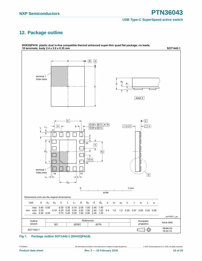
12. Package outline
Fig 7. Package outline SOT1442-1 (DHX2QFN18)
PTN36043 All information provided in this document is subject to legal disclaimers. © NXP Semiconductors N.V. 2018. All rights reserved.
Product data sheet Rev. 2 — 19 February 2018 16 of 29
NXP Semiconductors PTN36043USB Type-C SuperSpeed active switch
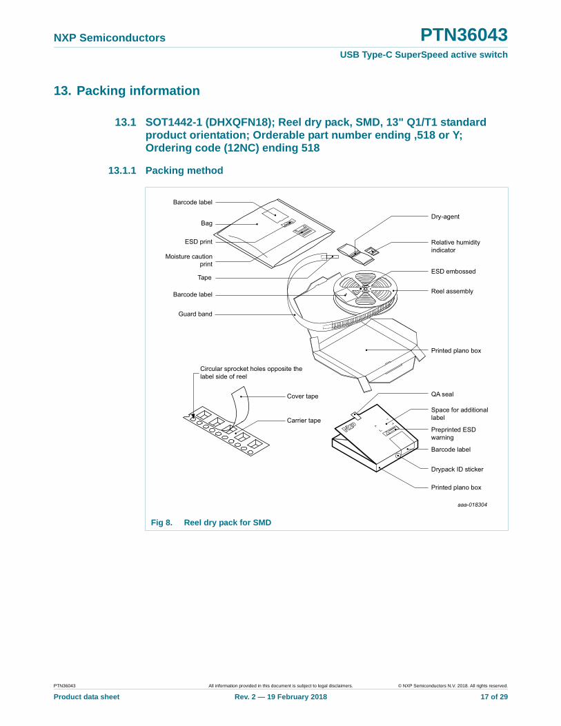
13. Packing information
13.1 SOT1442-1 (DHXQFN18); Reel dry pack, SMD, 13" Q1/T1 standard product orientation; Orderable part number ending ,518 or Y; Ordering code (12NC) ending 518
13.1.1 Packing method
Fig 8. Reel dry pack for SMD
PTN36043 All information provided in this document is subject to legal disclaimers. © NXP Semiconductors N.V. 2018. All rights reserved.
Product data sheet Rev. 2 — 19 February 2018 17 of 29
NXP Semiconductors PTN36043USB Type-C SuperSpeed active switch
[1] d = reel diameter; w = tape width.
[2] Packing quantity dependent on specific product type.
View ordering and availability details at NXP order portal, or contact your local NXP representative.
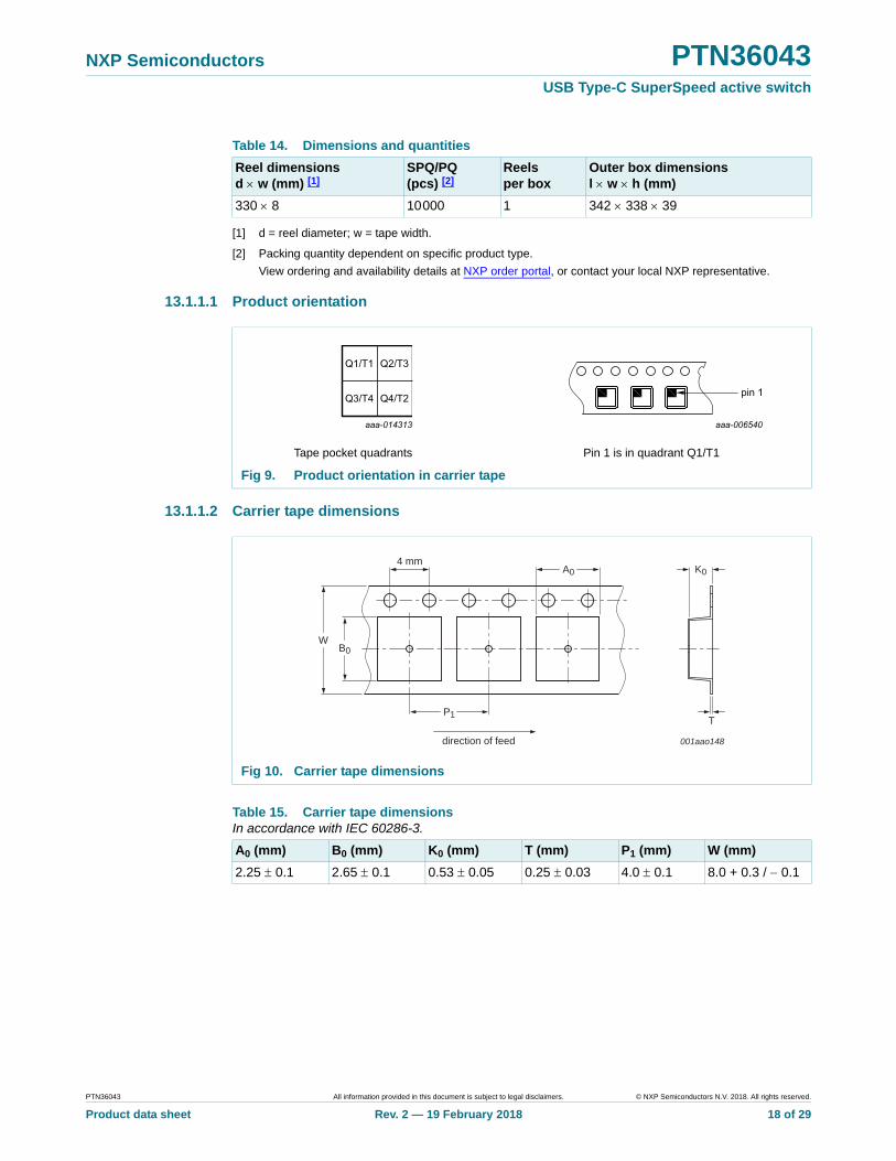
13.1.1.1 Product orientation
13.1.1.2 Carrier tape dimensions
Table 14. Dimensions and quantities
Reel dimensionsd w (mm) [1]
SPQ/PQ(pcs) [2]
Reelsper box
Outer box dimensionsl w h (mm)
330 8 10 000 1 342 338 39
Tape pocket quadrants Pin 1 is in quadrant Q1/T1
Fig 9. Product orientation in carrier tape
Fig 10. Carrier tape dimensions
Table 15. Carrier tape dimensionsIn accordance with IEC 60286-3.
A0 (mm) B0 (mm) K0 (mm) T (mm) P1 (mm) W (mm)
2.25 0.1 2.65 0.1 0.53 0.05 0.25 0.03 4.0 0.1 8.0 + 0.3 / 0.1
K0
001aao148
A04 mm
TP1
B0W
direction of feed
PTN36043 All information provided in this document is subject to legal disclaimers. © NXP Semiconductors N.V. 2018. All rights reserved.
Product data sheet Rev. 2 — 19 February 2018 18 of 29
NXP Semiconductors PTN36043USB Type-C SuperSpeed active switch
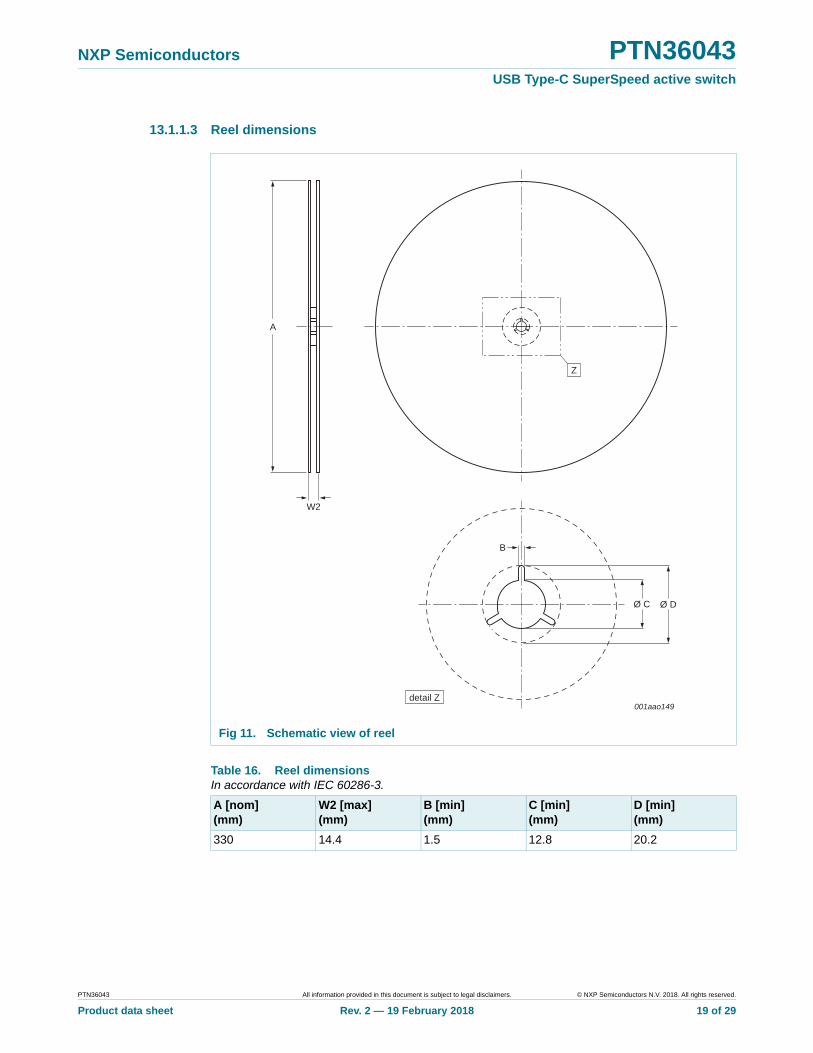
13.1.1.3 Reel dimensions
Fig 11. Schematic view of reel
Table 16. Reel dimensions In accordance with IEC 60286-3.
A [nom](mm)
W2 [max](mm)
B [min](mm)
C [min](mm)
D [min](mm)
330 14.4 1.5 12.8 20.2
detail Z
B
001aao149
W2
Ø C Ø D
A
Z
PTN36043 All information provided in this document is subject to legal disclaimers. © NXP Semiconductors N.V. 2018. All rights reserved.
Product data sheet Rev. 2 — 19 February 2018 19 of 29
NXP Semiconductors PTN36043USB Type-C SuperSpeed active switch
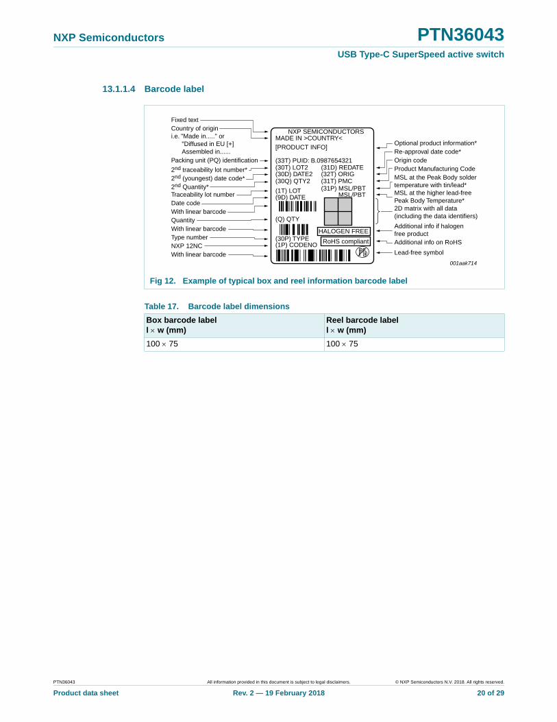
13.1.1.4 Barcode label
Fig 12. Example of typical box and reel information barcode label
Table 17. Barcode label dimensions
Box barcode labell w (mm)
Reel barcode labell w (mm)
100 75 100 75
001aak714
NXP SEMICONDUCTORSMADE IN >COUNTRY<[PRODUCT INFO]
(33T) PUID: B.0987654321(30T) LOT2(30D) DATE2(30Q) QTY2
(31D) REDATE(32T) ORIG(31T) PMC(31P) MSL/PBT
MSL/PBT
Optional product information*
Fixed textCountry of origini.e. "Made in....." or "Diffused in EU [+] Assembled in......Packing unit (PQ) identification
2nd traceability lot number*
Traceability lot numberDate codeWith linear barcode
With linear barcode
With linear barcode
Type numberNXP 12NC
Quantity
2nd (youngest) date code*2nd Quantity*
Re-approval date code*Origin codeProduct Manufacturing CodeMSL at the Peak Body soldertemperature with tin/lead*MSL at the higher lead-freePeak Body Temperature*2D matrix with all data(including the data identifiers)
Additional info if halogenfree productAdditional info on RoHS
Lead-free symbol
HALOGEN FREE
RoHS compliant
(1T) LOT(9D) DATE
(Q) QTY
(30P) TYPE(1P) CODENO
PTN36043 All information provided in this document is subject to legal disclaimers. © NXP Semiconductors N.V. 2018. All rights reserved.
Product data sheet Rev. 2 — 19 February 2018 20 of 29
NXP Semiconductors PTN36043USB Type-C SuperSpeed active switch
14. Soldering of SMD packages
This text provides a very brief insight into a complex technology. A more in-depth account of soldering ICs can be found in Application Note AN10365 “Surface mount reflow soldering description”.
14.1 Introduction to soldering
Soldering is one of the most common methods through which packages are attached to Printed Circuit Boards (PCBs), to form electrical circuits. The soldered joint provides both the mechanical and the electrical connection. There is no single soldering method that is ideal for all IC packages. Wave soldering is often preferred when through-hole and Surface Mount Devices (SMDs) are mixed on one printed wiring board; however, it is not suitable for fine pitch SMDs. Reflow soldering is ideal for the small pitches and high densities that come with increased miniaturization.
14.2 Wave and reflow soldering
Wave soldering is a joining technology in which the joints are made by solder coming from a standing wave of liquid solder. The wave soldering process is suitable for the following:
• Through-hole components
• Leaded or leadless SMDs, which are glued to the surface of the printed circuit board
Not all SMDs can be wave soldered. Packages with solder balls, and some leadless packages which have solder lands underneath the body, cannot be wave soldered. Also, leaded SMDs with leads having a pitch smaller than ~0.6 mm cannot be wave soldered, due to an increased probability of bridging.
The reflow soldering process involves applying solder paste to a board, followed by component placement and exposure to a temperature profile. Leaded packages, packages with solder balls, and leadless packages are all reflow solderable.
Key characteristics in both wave and reflow soldering are:
• Board specifications, including the board finish, solder masks and vias
• Package footprints, including solder thieves and orientation
• The moisture sensitivity level of the packages
• Package placement
• Inspection and repair
• Lead-free soldering versus SnPb soldering
14.3 Wave soldering
Key characteristics in wave soldering are:
• Process issues, such as application of adhesive and flux, clinching of leads, board transport, the solder wave parameters, and the time during which components are exposed to the wave
• Solder bath specifications, including temperature and impurities
PTN36043 All information provided in this document is subject to legal disclaimers. © NXP Semiconductors N.V. 2018. All rights reserved.
Product data sheet Rev. 2 — 19 February 2018 21 of 29
NXP Semiconductors PTN36043USB Type-C SuperSpeed active switch
14.4 Reflow soldering
Key characteristics in reflow soldering are:
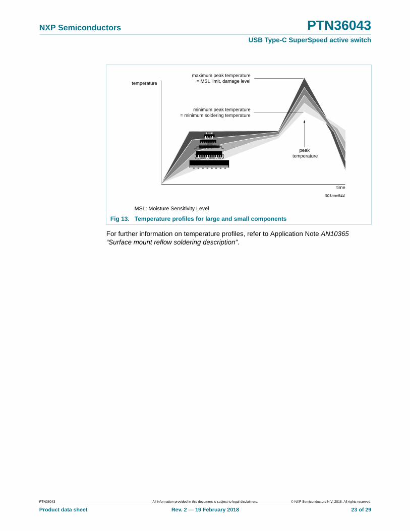
• Lead-free versus SnPb soldering; note that a lead-free reflow process usually leads to higher minimum peak temperatures (see Figure 13) than a SnPb process, thus reducing the process window
• Solder paste printing issues including smearing, release, and adjusting the process window for a mix of large and small components on one board
• Reflow temperature profile; this profile includes preheat, reflow (in which the board is heated to the peak temperature) and cooling down. It is imperative that the peak temperature is high enough for the solder to make reliable solder joints (a solder paste characteristic). In addition, the peak temperature must be low enough that the packages and/or boards are not damaged. The peak temperature of the package depends on package thickness and volume and is classified in accordance with Table 18 and 19
Moisture sensitivity precautions, as indicated on the packing, must be respected at all times.
Studies have shown that small packages reach higher temperatures during reflow soldering, see Figure 13.
Table 18. SnPb eutectic process (from J-STD-020D)
Package thickness (mm) Package reflow temperature (C)
Volume (mm3)
< 350 350
< 2.5 235 220
2.5 220 220
Table 19. Lead-free process (from J-STD-020D)
Package thickness (mm) Package reflow temperature (C)
Volume (mm3)
< 350 350 to 2 000 > 2 000
< 1.6 260 260 260
1.6 to 2.5 260 250 245
> 2.5 250 245 245
PTN36043 All information provided in this document is subject to legal disclaimers. © NXP Semiconductors N.V. 2018. All rights reserved.
Product data sheet Rev. 2 — 19 February 2018 22 of 29
NXP Semiconductors PTN36043USB Type-C SuperSpeed active switch
For further information on temperature profiles, refer to Application Note AN10365 “Surface mount reflow soldering description”.
MSL: Moisture Sensitivity Level
Fig 13. Temperature profiles for large and small components
001aac844
temperature
time
minimum peak temperature= minimum soldering temperature
maximum peak temperature= MSL limit, damage level
peak temperature
PTN36043 All information provided in this document is subject to legal disclaimers. © NXP Semiconductors N.V. 2018. All rights reserved.
Product data sheet Rev. 2 — 19 February 2018 23 of 29
NXP Semiconductors PTN36043USB Type-C SuperSpeed active switch
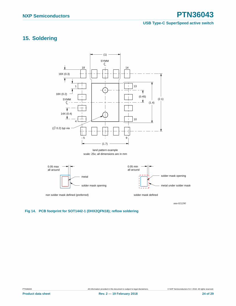
15. Soldering
Fig 14. PCB footprint for SOT1442-1 (DHX2QFN18); reflow soldering
18X (0.2)
18X (0.3)
( 0.2) typ via
14X (0.4)
(2.1)
(1.7)
(0.45)
(1)
(1.4)
SYMM
1
4
5 9
10
13
1418
SYMM
aaa-021290
0.05 minall around
0.05 maxall around
land pattern examplescale: 25x; all dimensions are in mm
solder mask opening
metal under solder mask
solder mask defined
metal
solder mask opening
non solder mask defined (preferred)
PTN36043 All information provided in this document is subject to legal disclaimers. © NXP Semiconductors N.V. 2018. All rights reserved.
Product data sheet Rev. 2 — 19 February 2018 24 of 29
NXP Semiconductors PTN36043USB Type-C SuperSpeed active switch
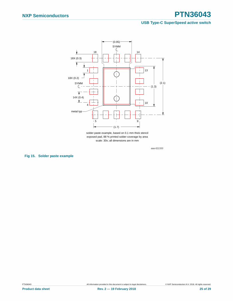
Fig 15. Solder paste example
18X (0.2)
18X (0.3)
metal typ
14X (0.4)
(2.1)
(1.7)
(0.95)
(1.3)
1
4
5 9
10
13
1418
SYMM
solder paste example, based on 0.1 mm thick stencilexposed pad, 88 % printed solder coverage by area
scale: 30x; all dimensions are in mm
SYMM
aaa-021333
PTN36043 All information provided in this document is subject to legal disclaimers. © NXP Semiconductors N.V. 2018. All rights reserved.
Product data sheet Rev. 2 — 19 February 2018 25 of 29

NXP Semiconductors PTN36043USB Type-C SuperSpeed active switch
16. Abbreviations
17. Revision history
Table 20. Abbreviations
Acronym Description
A/V Audio/Video device
AIO All In One computer platform
CDM Charged-Device Model
CMOS Complementary Metal-Oxide Semiconductor
ESD ElectroStatic Discharge
HBM Human Body Model
I2C-bus Inter-Integrated Circuit bus
I/O Input/Output
IC Integrated Circuit
ISI InterSymbol Interference
LFPS Low Frequency Periodic Signaling
PCB Printed-Circuit Board
RX Receive (or Receiver)
SI Signal Integrity
TX Transmit (or Transmitter)
USB Universal Serial Bus
Table 21. Revision history
Document ID Release date Data sheet status Change notice Supersedes
PTN36043 v.2 20180219 Product data sheet - PTN36043 v.1.3
Modifications: • Table 3 “Pin description” and Table 6 “SEL input setting”: Updated description for pin SEL from “in high impedance state for USB Type-C Safe State support” to “connected to VDD thru low ohmic resistor (50 )”
PTN36043 v.1.3 20171117 Product data sheet - PTN36043 v.1.2
Modifications: • Table 3 “Pin description” and Table 6 “SEL input setting”: Updated description for pin SEL from “connected to VDD thru low ohmic resistor (50 )” to “in high impedance state for USB Type-C Safe State support”
PTN36043 v.1.2 20160822 Product data sheet - PTN36043 v.1.1
Modifications: • Full DS release to web; replaces short data sheet PTN36043_SDS
PTN36043 v.1.1 20160802 Product data sheet - PTN36043 v.1
Modifications: • Table 2 “Ordering options”: Removed 500 piece minimum order quantity
PTN36043 v.1 20160415 Product data sheet - -
PTN36043 All information provided in this document is subject to legal disclaimers. © NXP Semiconductors N.V. 2018. All rights reserved.
Product data sheet Rev. 2 — 19 February 2018 26 of 29
NXP Semiconductors PTN36043USB Type-C SuperSpeed active switch
18. Legal information
18.1 Data sheet status
[1] Please consult the most recently issued document before initiating or completing a design.
[2] The term ‘short data sheet’ is explained in section “Definitions”.
[3] The product status of device(s) described in this document may have changed since this document was published and may differ in case of multiple devices. The latest product status information is available on the Internet at URL http://www.nxp.com.
18.2 Definitions
Draft — The document is a draft version only. The content is still under internal review and subject to formal approval, which may result in modifications or additions. NXP Semiconductors does not give any representations or warranties as to the accuracy or completeness of information included herein and shall have no liability for the consequences of use of such information.
Short data sheet — A short data sheet is an extract from a full data sheet with the same product type number(s) and title. A short data sheet is intended for quick reference only and should not be relied upon to contain detailed and full information. For detailed and full information see the relevant full data sheet, which is available on request via the local NXP Semiconductors sales office. In case of any inconsistency or conflict with the short data sheet, the full data sheet shall prevail.
Product specification — The information and data provided in a Product data sheet shall define the specification of the product as agreed between NXP Semiconductors and its customer, unless NXP Semiconductors and customer have explicitly agreed otherwise in writing. In no event however, shall an agreement be valid in which the NXP Semiconductors product is deemed to offer functions and qualities beyond those described in the Product data sheet.
18.3 Disclaimers
Limited warranty and liability — Information in this document is believed to be accurate and reliable. However, NXP Semiconductors does not give any representations or warranties, expressed or implied, as to the accuracy or completeness of such information and shall have no liability for the consequences of use of such information. NXP Semiconductors takes no responsibility for the content in this document if provided by an information source outside of NXP Semiconductors.
In no event shall NXP Semiconductors be liable for any indirect, incidental, punitive, special or consequential damages (including - without limitation - lost profits, lost savings, business interruption, costs related to the removal or replacement of any products or rework charges) whether or not such damages are based on tort (including negligence), warranty, breach of contract or any other legal theory.
Notwithstanding any damages that customer might incur for any reason whatsoever, NXP Semiconductors’ aggregate and cumulative liability towards customer for the products described herein shall be limited in accordance with the Terms and conditions of commercial sale of NXP Semiconductors.
Right to make changes — NXP Semiconductors reserves the right to make changes to information published in this document, including without limitation specifications and product descriptions, at any time and without notice. This document supersedes and replaces all information supplied prior to the publication hereof.
Suitability for use — NXP Semiconductors products are not designed, authorized or warranted to be suitable for use in life support, life-critical or safety-critical systems or equipment, nor in applications where failure or malfunction of an NXP Semiconductors product can reasonably be expected to result in personal injury, death or severe property or environmental damage. NXP Semiconductors and its suppliers accept no liability for inclusion and/or use of NXP Semiconductors products in such equipment or applications and therefore such inclusion and/or use is at the customer’s own risk.
Applications — Applications that are described herein for any of these products are for illustrative purposes only. NXP Semiconductors makes no representation or warranty that such applications will be suitable for the specified use without further testing or modification.
Customers are responsible for the design and operation of their applications and products using NXP Semiconductors products, and NXP Semiconductors accepts no liability for any assistance with applications or customer product design. It is customer’s sole responsibility to determine whether the NXP Semiconductors product is suitable and fit for the customer’s applications and products planned, as well as for the planned application and use of customer’s third party customer(s). Customers should provide appropriate design and operating safeguards to minimize the risks associated with their applications and products.
NXP Semiconductors does not accept any liability related to any default, damage, costs or problem which is based on any weakness or default in the customer’s applications or products, or the application or use by customer’s third party customer(s). Customer is responsible for doing all necessary testing for the customer’s applications and products using NXP Semiconductors products in order to avoid a default of the applications and the products or of the application or use by customer’s third party customer(s). NXP does not accept any liability in this respect.
Limiting values — Stress above one or more limiting values (as defined in the Absolute Maximum Ratings System of IEC 60134) will cause permanent damage to the device. Limiting values are stress ratings only and (proper) operation of the device at these or any other conditions above those given in the Recommended operating conditions section (if present) or the Characteristics sections of this document is not warranted. Constant or repeated exposure to limiting values will permanently and irreversibly affect the quality and reliability of the device.
Terms and conditions of commercial sale — NXP Semiconductors products are sold subject to the general terms and conditions of commercial sale, as published at http://www.nxp.com/profile/terms, unless otherwise agreed in a valid written individual agreement. In case an individual agreement is concluded only the terms and conditions of the respective agreement shall apply. NXP Semiconductors hereby expressly objects to applying the customer’s general terms and conditions with regard to the purchase of NXP Semiconductors products by customer.
No offer to sell or license — Nothing in this document may be interpreted or construed as an offer to sell products that is open for acceptance or the grant, conveyance or implication of any license under any copyrights, patents or other industrial or intellectual property rights.
Document status[1][2] Product status[3] Definition
Objective [short] data sheet Development This document contains data from the objective specification for product development.
Preliminary [short] data sheet Qualification This document contains data from the preliminary specification.
Product [short] data sheet Production This document contains the product specification.
PTN36043 All information provided in this document is subject to legal disclaimers. © NXP Semiconductors N.V. 2018. All rights reserved.
Product data sheet Rev. 2 — 19 February 2018 27 of 29
NXP Semiconductors PTN36043USB Type-C SuperSpeed active switch
Export control — This document as well as the item(s) described herein may be subject to export control regulations. Export might require a prior authorization from competent authorities.
Non-automotive qualified products — Unless this data sheet expressly states that this specific NXP Semiconductors product is automotive qualified, the product is not suitable for automotive use. It is neither qualified nor tested in accordance with automotive testing or application requirements. NXP Semiconductors accepts no liability for inclusion and/or use of non-automotive qualified products in automotive equipment or applications.
In the event that customer uses the product for design-in and use in automotive applications to automotive specifications and standards, customer (a) shall use the product without NXP Semiconductors’ warranty of the product for such automotive applications, use and specifications, and (b) whenever customer uses the product for automotive applications beyond
NXP Semiconductors’ specifications such use shall be solely at customer’s own risk, and (c) customer fully indemnifies NXP Semiconductors for any liability, damages or failed product claims resulting from customer design and use of the product for automotive applications beyond NXP Semiconductors’ standard warranty and NXP Semiconductors’ product specifications.
Translations — A non-English (translated) version of a document is for reference only. The English version shall prevail in case of any discrepancy between the translated and English versions.
18.4 TrademarksNotice: All referenced brands, product names, service names and trademarks are the property of their respective owners.
19. Contact information
For more information, please visit: http://www.nxp.com
For sales office addresses, please send an email to: [email protected]
PTN36043 All information provided in this document is subject to legal disclaimers. © NXP Semiconductors N.V. 2018. All rights reserved.
Product data sheet Rev. 2 — 19 February 2018 28 of 29
NXP Semiconductors PTN36043USB Type-C SuperSpeed active switch
20. Contents
1 General description . . . . . . . . . . . . . . . . . . . . . . 1
2 Features and benefits . . . . . . . . . . . . . . . . . . . . 1
3 Applications . . . . . . . . . . . . . . . . . . . . . . . . . . . . 2
4 Ordering information. . . . . . . . . . . . . . . . . . . . . 24.1 Ordering options . . . . . . . . . . . . . . . . . . . . . . . . 2
5 Block diagram . . . . . . . . . . . . . . . . . . . . . . . . . . 3
6 Pinning information. . . . . . . . . . . . . . . . . . . . . . 46.1 Pinning . . . . . . . . . . . . . . . . . . . . . . . . . . . . . . . 46.2 Pin description . . . . . . . . . . . . . . . . . . . . . . . . . 4
7 Functional description . . . . . . . . . . . . . . . . . . . 67.1 Receive equalization, transmitter de-emphasis
and output swing level controls . . . . . . . . . . . . 67.2 Device states and power management . . . . . . 77.3 SEL input pin . . . . . . . . . . . . . . . . . . . . . . . . . . 8
8 Application guideline for Control of CHx_SETx and SEL input pins . . . . . . . . . . . . . . . . . . . . . . 8
9 Limiting values. . . . . . . . . . . . . . . . . . . . . . . . . . 9
10 Recommended operating conditions. . . . . . . . 9
11 Characteristics. . . . . . . . . . . . . . . . . . . . . . . . . 1011.1 Device characteristics. . . . . . . . . . . . . . . . . . . 1011.2 Receiver AC/DC characteristics . . . . . . . . . . . 1211.3 Transmitter AC/DC characteristics . . . . . . . . . 1311.4 Ternary control inputs . . . . . . . . . . . . . . . . . . . 14
12 Package outline . . . . . . . . . . . . . . . . . . . . . . . . 16
13 Packing information . . . . . . . . . . . . . . . . . . . . 1713.1 SOT1442-1 (DHXQFN18); Reel dry pack, SMD,
13" Q1/T1 standard product orientation; Orderable part number ending ,518 or Y; Ordering code (12NC) ending 518 . . . . . . . . . . . . . . . . 17
13.1.1 Packing method . . . . . . . . . . . . . . . . . . . . . . . 1713.1.1.1 Product orientation . . . . . . . . . . . . . . . . . . . . . 1813.1.1.2 Carrier tape dimensions . . . . . . . . . . . . . . . . . 1813.1.1.3 Reel dimensions . . . . . . . . . . . . . . . . . . . . . . . 1913.1.1.4 Barcode label . . . . . . . . . . . . . . . . . . . . . . . . . 20
14 Soldering of SMD packages . . . . . . . . . . . . . . 2114.1 Introduction to soldering . . . . . . . . . . . . . . . . . 2114.2 Wave and reflow soldering . . . . . . . . . . . . . . . 2114.3 Wave soldering . . . . . . . . . . . . . . . . . . . . . . . . 2114.4 Reflow soldering . . . . . . . . . . . . . . . . . . . . . . . 22
15 Soldering . . . . . . . . . . . . . . . . . . . . . . . . . . . . . 24
16 Abbreviations. . . . . . . . . . . . . . . . . . . . . . . . . . 26
17 Revision history. . . . . . . . . . . . . . . . . . . . . . . . 26
18 Legal information. . . . . . . . . . . . . . . . . . . . . . . 2718.1 Data sheet status . . . . . . . . . . . . . . . . . . . . . . 27
18.2 Definitions . . . . . . . . . . . . . . . . . . . . . . . . . . . 2718.3 Disclaimers . . . . . . . . . . . . . . . . . . . . . . . . . . 2718.4 Trademarks . . . . . . . . . . . . . . . . . . . . . . . . . . 28
19 Contact information . . . . . . . . . . . . . . . . . . . . 28
20 Contents. . . . . . . . . . . . . . . . . . . . . . . . . . . . . . 29
© NXP Semiconductors N.V. 2018. All rights reserved.
For more information, please visit: http://www.nxp.comFor sales office addresses, please send an email to: [email protected]
Date of release: 19 February 2018
Document identifier: PTN36043
Please be aware that important notices concerning this document and the product(s) described herein, have been included in section ‘Legal information’.