Embed Size (px)
Citation preview
SingMai Electronics
PT55 User Manual Revision 0.8 Page 1 of 32
PT55
Advanced CompositeVideo Interface:Encoder IP Core
User Manual
Revision 0.811th November 2016
SingMai Electronics
PT55 User Manual Revision 0.8 Page 2 of 32
Revisions
Date Revisions Version
01-05-2016 First Draft. 0.1
28-05-2106 Timing diagrams updated.Block diagram updated.
0.2
13-07-2016 1080i standards added.IP core resource usage added.aCVi description modified.Data transfer description added.Cable compensation description added.Simulation information added.Altera encryption description added.
0.3
17-07-2016 FPGA resource use updated.Reg_clk port removed.Insertion test signal modified.Data transmit register locations corrected.Register address range changed to A[4:0].Text corrections and additions.
0.4
09-08-2016 Luma interpolation added.Chroma interpolation filter modified.Subcarrier frequencies modified.aCVi description modified.Data slicing schematic updated.Output interface schematic updated.
0.5
25-08-2016 Verilog modules renamed.Some ports renamed.NTSC-M/PAL/NTSC-960H and PAL-960Hstandards added.SD chroma filters added.Input formatting added.
0.6
21-09-2016 aCVi 0.5 format added. 0.7
11-11-2016 aCVI 0.5 format removed.Changes to data transfer control.Changes to auto cable compensation.Additional luma interpolation filter added (foralternative analogue HD formats).Chroma interpolation filter redesigned.
0.8
SingMai Electronics
PT55 User Manual Revision 0.8 Page 3 of 32
Contents
Revisions .................................................................................................................................................. 2Contents................................................................................................................................................... 3Tables ....................................................................................................................................................... 3Figures...................................................................................................................................................... 31. Introduction ................................................................................................................................... 52. PT55 Module description...............................................................................................................63. Signal Interconnections................................................................................................................. 74. aCVi Overview .............................................................................................................................. 105. Technical Overview.......................................................................................................................12
PT55_encoder.v .................................................................................................................................12Register_control.v .............................................................................................................................12Yin.v ....................................................................................................................................................12Cin.v ....................................................................................................................................................15SPG.v ..................................................................................................................................................17Modulator.v ...................................................................................................................................... 19Preemphasis.v................................................................................................................................... 19
6. aCVi Cable Compensation............................................................................................................ 227. Data Transfers .............................................................................................................................. 248. Register interface ........................................................................................................................ 279. Register descriptions ...................................................................................................................2810. Output Interface.......................................................................................................................3011. Altera Encrypted files .................................................................................................................. 32
Tables
Table 1 PT55 Altera FPGA resource requirements.................................................................................. 5Table 2 PT55 Verilog file structure. .........................................................................................................6Table 3 PT55 Input/Output signals..........................................................................................................8Table 4 aCVi supported video formats. ................................................................................................ 10Table 5 PT55 Input video formats..........................................................................................................13Table 6 Line and subcarrier frequencies (aCVi and SD). ...................................................................... 19Table 8 Register Descriptions. ..............................................................................................................29Table 9 Encrypted file naming. ............................................................................................................. 32
Figures
Figure 1 PT55 Block schematic. ............................................................................................................... 7Figure 2 aCVi Spectrum. ......................................................................................................................... 11Figure 3 PT55 Block diagram. .................................................................................................................12Figure 4 Input chroma demultiplexing modes......................................................................................13Figure 5 Luma interpolator filter frequency response (aCVi).............................................................. 14Figure 6 NTSC/PAL Luma interpolation filter (27MHz). ....................................................................... 14Figure 7 Luma interpolator filter frequency response (Control Register 2, bit 4 = '1'). ......................15Figure 8 Cb/Cr Interpolation filter response (aCVi).............................................................................. 16Figure 9 Cb/Cr Interpolation filter response (NTSC/PAL). ................................................................... 16Figure 10 720p/60 Horizontal Timing. ....................................................................................................17Figure 11 720p/50-60Hz Vertical Timing. ............................................................................................... 18Figure 12 1080p/30 Horizontal Timing................................................................................................... 18Figure 13 1080p/25-30Hz Vertical Timing. ............................................................................................. 18Figure 14 Sinx/x Filter response. ...........................................................................................................20Figure 15 Pre-emphasis filter response - RG59 cable. ..........................................................................20Figure 16 aCVi output, 30MHz sweep (Pre-emphasis = minimum). .....................................................21
SingMai Electronics
PT55 User Manual Revision 0.8 Page 4 of 32
Figure 17 aCVi output, 30MHz sweep (Pre-emphasis = maximum)......................................................21Figure 18 Coaxial cable frequency response. ....................................................................................... 22Figure 19 Insertion test signal. .............................................................................................................. 23Figure 20 Data transfer protocol. ......................................................................................................... 24Figure 21 Data slicing schematic. .......................................................................................................... 25Figure 22 PT55 Register control. ........................................................................................................... 27Figure 23 PT55 output interface schematic...........................................................................................31
SingMai Electronics
PT55 User Manual Revision 0.8 Page 5 of 32
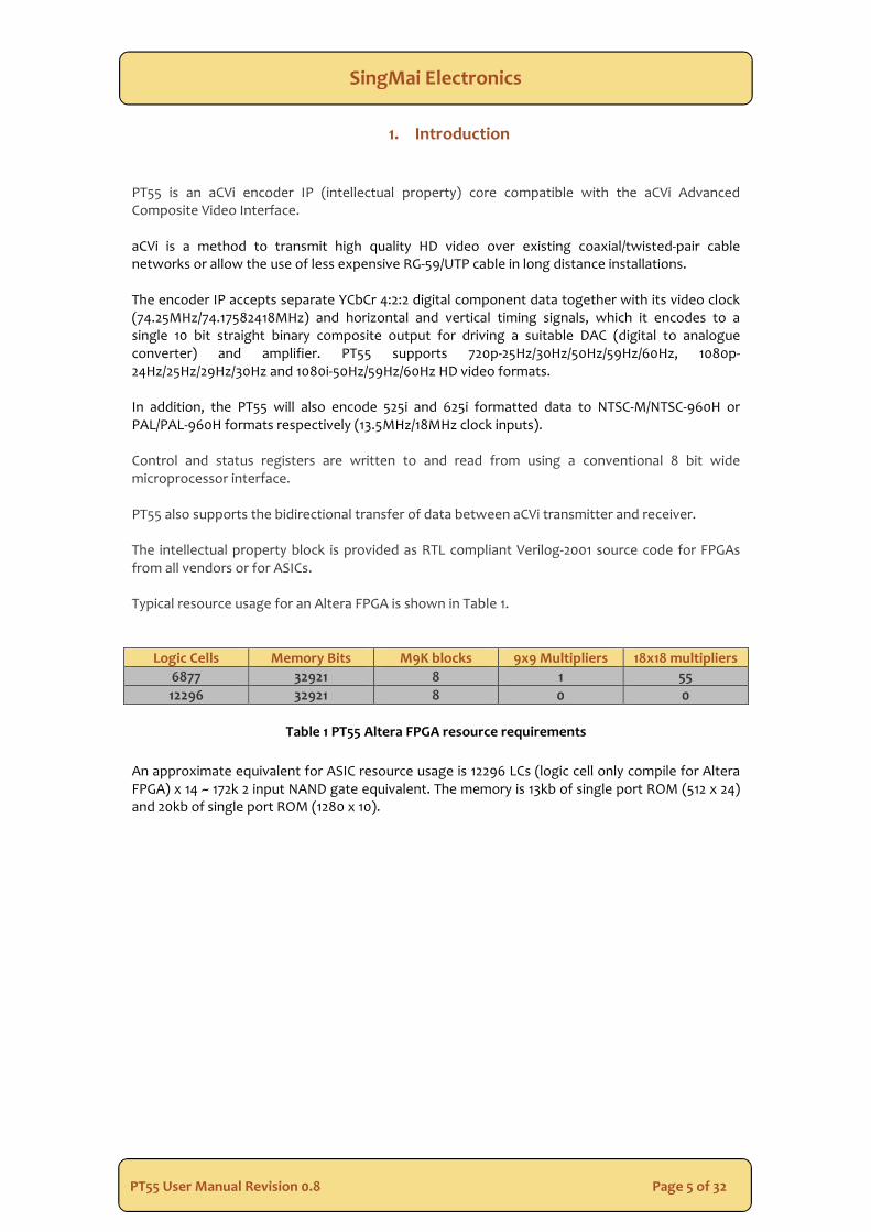
1. Introduction
PT55 is an aCVi encoder IP (intellectual property) core compatible with the aCVi AdvancedComposite Video Interface.
aCVi is a method to transmit high quality HD video over existing coaxial/twisted-pair cablenetworks or allow the use of less expensive RG-59/UTP cable in long distance installations.
The encoder IP accepts separate YCbCr 4:2:2 digital component data together with its video clock(74.25MHz/74.17582418MHz) and horizontal and vertical timing signals, which it encodes to asingle 10 bit straight binary composite output for driving a suitable DAC (digital to analogueconverter) and amplifier. PT55 supports 720p-25Hz/30Hz/50Hz/59Hz/60Hz, 1080p-24Hz/25Hz/29Hz/30Hz and 1080i-50Hz/59Hz/60Hz HD video formats.
In addition, the PT55 will also encode 525i and 625i formatted data to NTSC-M/NTSC-960H orPAL/PAL-960H formats respectively (13.5MHz/18MHz clock inputs).
Control and status registers are written to and read from using a conventional 8 bit widemicroprocessor interface.
PT55 also supports the bidirectional transfer of data between aCVi transmitter and receiver.
The intellectual property block is provided as RTL compliant Verilog-2001 source code for FPGAsfrom all vendors or for ASICs.
Typical resource usage for an Altera FPGA is shown in Table 1.
Logic Cells Memory Bits M9K blocks 9x9 Multipliers 18x18 multipliers
6877 32921 8 1 55
12296 32921 8 0 0
Table 1 PT55 Altera FPGA resource requirements
An approximate equivalent for ASIC resource usage is 12296 LCs (logic cell only compile for AlteraFPGA) x 14 ~ 172k 2 input NAND gate equivalent. The memory is 13kb of single port ROM (512 x 24)and 20kb of single port ROM (1280 x 10).
SingMai Electronics
PT55 User Manual Revision 0.8 Page 6 of 32
2. PT55 Module description
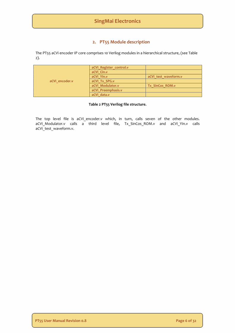
The PT55 aCVi encoder IP core comprises 10 Verilog modules in a hierarchical structure, (see Table2).
aCVi_encoder.v
aCVI_Register_control.v
aCVi_Cin.v
aCVi_Yin.v aCVi_test_waveform.v
aCVI_Tx_SPG.v
aCVi_Modulator.v Tx_SinCos_ROM.v
aCVi_Preemphasis.v
aCVi_data.v
Table 2 PT55 Verilog file structure.
The top level file is aCVi_encoder.v which, in turn, calls seven of the other modules.aCVi_Modulator.v calls a third level file, Tx_SinCos_ROM.v and aCVi_Yin.v callsaCVi_test_waveform.v.
SingMai Electronics
PT55 User Manual Revision 0.8 Page 7 of 32
3. Signal Interconnections
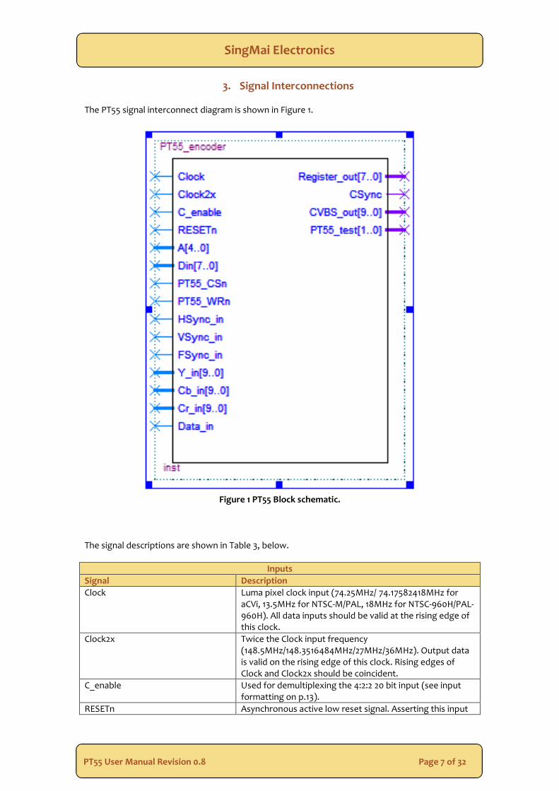
The PT55 signal interconnect diagram is shown in Figure 1.
Figure 1 PT55 Block schematic.
The signal descriptions are shown in Table 3, below.
Inputs
Signal Description
Clock Luma pixel clock input (74.25MHz/ 74.17582418MHz foraCVi, 13.5MHz for NTSC-M/PAL, 18MHz for NTSC-960H/PAL-960H). All data inputs should be valid at the rising edge ofthis clock.
Clock2x Twice the Clock input frequency(148.5MHz/148.3516484MHz/27MHz/36MHz). Output datais valid on the rising edge of this clock. Rising edges ofClock and Clock2x should be coincident.
C_enable Used for demultiplexing the 4:2:2 20 bit input (see inputformatting on p.13).
RESETn Asynchronous active low reset signal. Asserting this input
SingMai Electronics
PT55 User Manual Revision 0.8 Page 8 of 32
sets all the control registers to their default value andresets all registers.
A[4:0] Control address bus input used to select the controlregister to be written to/read from.
Din[7:0] Control data input bus.
PT55_CSn Control chip select input, active low. Used in combinationwith the WRn input to control writing to the controlregisters.
PT55_WRn Active low write enable input. Used in combination withthe CSn input to control writing to the control registers.
HSync_in Horizontal synchronization input. For 720p/60Hz operationthis input is at 45kHz. Active low input, the falling edge isthe 0H timing reference point. This input must be at least 4‘Clock’ periods wide. (See input formatting on p.12).
VSync_in Vertical synchronization input. For 720p/60Hz operationthis input is at 60Hz. Active low input, the falling edge isthe 0V timing reference point. This input must be at least 4‘Clock’ periods wide. (See input formatting on p.12).
FSync_in Frame synchronization input. For interlaced inputs thisinput indicates the first (=’0’) or second (=’1’) field of theframe. For non-interlaced inputs this input should be tiedto ‘0’. (See input formatting on p.12).
Y_in[9:0] Y (luma) input or BT1120 MSB input to the encoder. If luma,the input is straight binary, blanking level is 6410 and peaklevel 96010. The data input should be valid at the risingedge of ‘Clock’. Y_in[9] is the MSB. If the input is 8-bitswide, the bottom 2 bits should be tied to ‘0’. (See inputformatting on p.13).
Cb_in[9:0] Cb (B-Y chroma) input or Cb/Cr multiplexed input to theencoder or BT1120 LSB. If chroma the input is offset binary,blanking level is 51210. The data input should be valid at therising edge of ‘Clock’. Cb_in[9] is the MSB. If the input is 8-bits wide, the bottom 2 bits should be tied to ‘0’. (Seeinput formatting on p.13).
Cr_in[9:0] Cr (R-Y chroma) input to the encoder. The input is offsetbinary, blanking level is 51210. The data input should bevalid at the rising edge of ‘Clock’. Cr_in[9] is the MSB. If theinput is 8-bits wide, the bottom 2 bits should be tied to ‘0’.(See input formatting on p.13).
Data_in Sliced data input from the aCVi receiver (see Chapter 7).
Outputs
Signal Description
Register_out[7:0] Control output data bus. Outputs the control/statusregister data selected by the A[4:0] bus.
CSync Digital composite sync output.
CVBS_out[9:0] Encoded aCVi/NTSC/PAL output data. CVBS_out[9] is theMSB. The output is straight binary coded and is valid at therising edge of ‘Clock2x’.
Table 3 PT55 Input/Output signals
SingMai Electronics
PT55 User Manual Revision 0.8 Page 9 of 32
The Verilog instantiation of PT55 is shown below:
PT55_encoder PT55_encoder_inst(.Clock(Clock_sig) , // input Clock_sig.Clock2x(Clock2x_sig) , // input Clock2x_sig.C_enable(C_enable_sig) , // input C_enable_sig.RESETn(RESETn_sig) , // input RESETn_sig.A(A_sig) , // input [4:0] A_sig.Din(Din_sig) , // input [7:0] Din_sig.PT55_CSn(PT55_CSn_sig) , // input PT55_CSn_sig.PT55_WRn(PT55_WRn_sig) , // input PT55_WRn_sig.HSync_in(HSync_in_sig) , // input HSync_in_sig.VSync_in(VSync_in_sig) , // input VSync_in_sig.FSync_in(FSync_in_sig) , // input FSync_in_sig.Y_in(Y_in_sig) , // input [9:0] Y_in_sig.Cb_in(Cb_in_sig) , // input [9:0] Cb_in_sig.Cr_in(Cr_in_sig) , // input [9:0] Cr_in_sig.Data_in(Data_in_sig) , // input Data_in_sig
.Register_out(Register_out_sig) , // output [7:0] Register_out_sig
.CSync(CSync_sig) , // output CSync_sig
.CVBS_out(CVBS_out_sig) // output [9:0] CVBS_out_sig);
SingMai Electronics
PT55 User Manual Revision 0.8 Page 10 of 32
4. aCVi Overview
The following is a brief overview of the aCVi interface.
The basic concept of the aCVi interface is to build on the proven and reliable transport method ofNTSC. NTSC transmissions are capable of transmitting more than 1km across RG-59 cable but thebandwidth is limited to 5MHz. Because the cable system is a closed system, it is only necessary forthe transmitter and receiver to ‘understand’ each other and we can modify the basic NTSC methodto suit HD transmissions.
There are two versions of aCVi; first we will describe the ‘full bandwidth’ version.
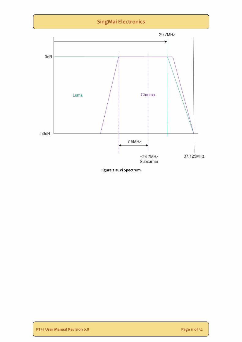
According to the SMPTE-296M specification, HD (74.25MHz sampling) video transmission requiresa luma bandwidth of 30MHz and chroma bandwidth of 15MHz. To save on system costs aCVisupports the 30MHz luma bandwidth but constrains the chroma bandwidth to 7.5MHz (4:1:1sampling).
The colour difference signals are modulated onto a carrier in quadrature so they effectively usethe same bandwidth: the chroma subcarrier is ~24.75MHz.. The high frequency luma and themodulated chroma overlap above 12.4MHz but because of the line to line phase relationship of thechroma, may be separated using a line comb filter (and also because of the use of single chipimage sensors, there is usually little high frequency content to cause image artifacts).
The effective bandwidth of the complete signal is therefore approximately 12.3MHz (chromaupper sideband + filter roll off) + 24.75MHz or about 37MHz, setting a minimum samplingfrequency of 2 x 37MHz or 74MHz. For convenience we choose 74.25MHz as a sampling frequencyas this is related to the SMPTE272M standard; (see Figure 2).
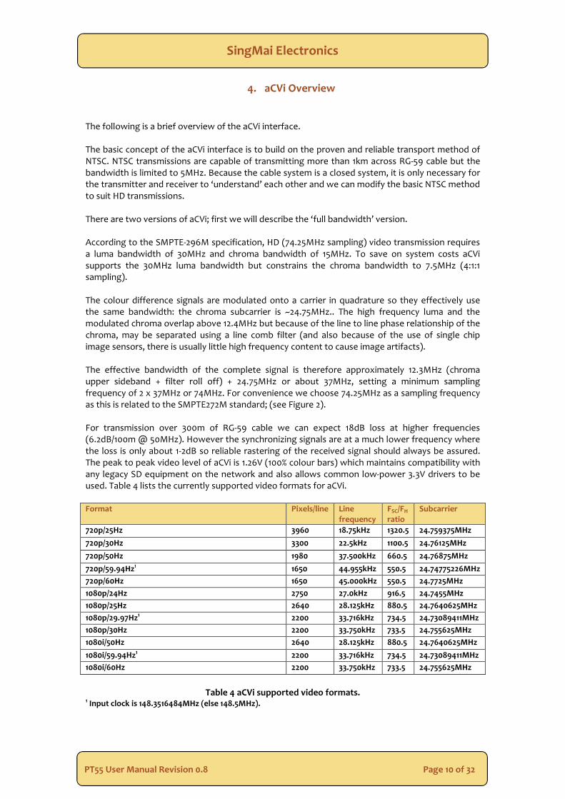
For transmission over 300m of RG-59 cable we can expect 18dB loss at higher frequencies(6.2dB/100m @ 50MHz). However the synchronizing signals are at a much lower frequency wherethe loss is only about 1-2dB so reliable rastering of the received signal should always be assured.The peak to peak video level of aCVi is 1.26V (100% colour bars) which maintains compatibility withany legacy SD equipment on the network and also allows common low-power 3.3V drivers to beused. Table 4 lists the currently supported video formats for aCVi.
Format Pixels/line Linefrequency
FSC/FH
ratioSubcarrier
720p/25Hz 3960 18.75kHz 1320.5 24.759375MHz
720p/30Hz 3300 22.5kHz 1100.5 24.76125MHz
720p/50Hz 1980 37.500kHz 660.5 24.76875MHz
720p/59.94Hz1 1650 44.955kHz 550.5 24.74775226MHz
720p/60Hz 1650 45.000kHz 550.5 24.7725MHz
1080p/24Hz 2750 27.0kHz 916.5 24.7455MHz
1080p/25Hz 2640 28.125kHz 880.5 24.7640625MHz
1080p/29.97Hz1 2200 33.716kHz 734.5 24.73089411MHz
1080p/30Hz 2200 33.750kHz 733.5 24.755625MHz
1080i/50Hz 2640 28.125kHz 880.5 24.7640625MHz
1080i/59.94Hz1 2200 33.716kHz 734.5 24.73089411MHz
1080i/60Hz 2200 33.750kHz 733.5 24.755625MHz
Table 4 aCVi supported video formats.1 Input clock is 148.3516484MHz (else 148.5MHz).
SingMai Electronics
PT55 User Manual Revision 0.8 Page 11 of 32
Figure 2 aCVi Spectrum.
SingMai Electronics
PT55 User Manual Revision 0.8 Page 12 of 32
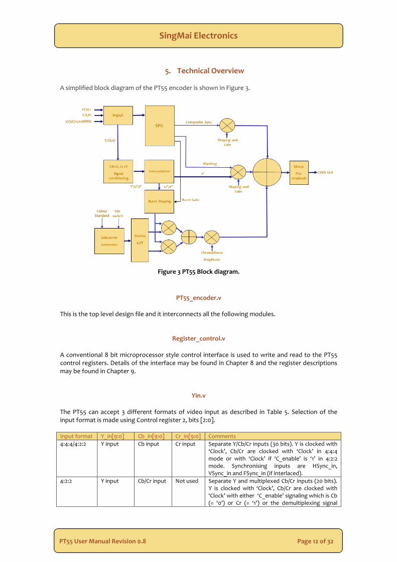
5. Technical Overview
A simplified block diagram of the PT55 encoder is shown in Figure 3.
Figure 3 PT55 Block diagram.
PT55_encoder.v
This is the top level design file and it interconnects all the following modules.
Register_control.v
A conventional 8 bit microprocessor style control interface is used to write and read to the PT55control registers. Details of the interface may be found in Chapter 8 and the register descriptionsmay be found in Chapter 9.
Yin.v
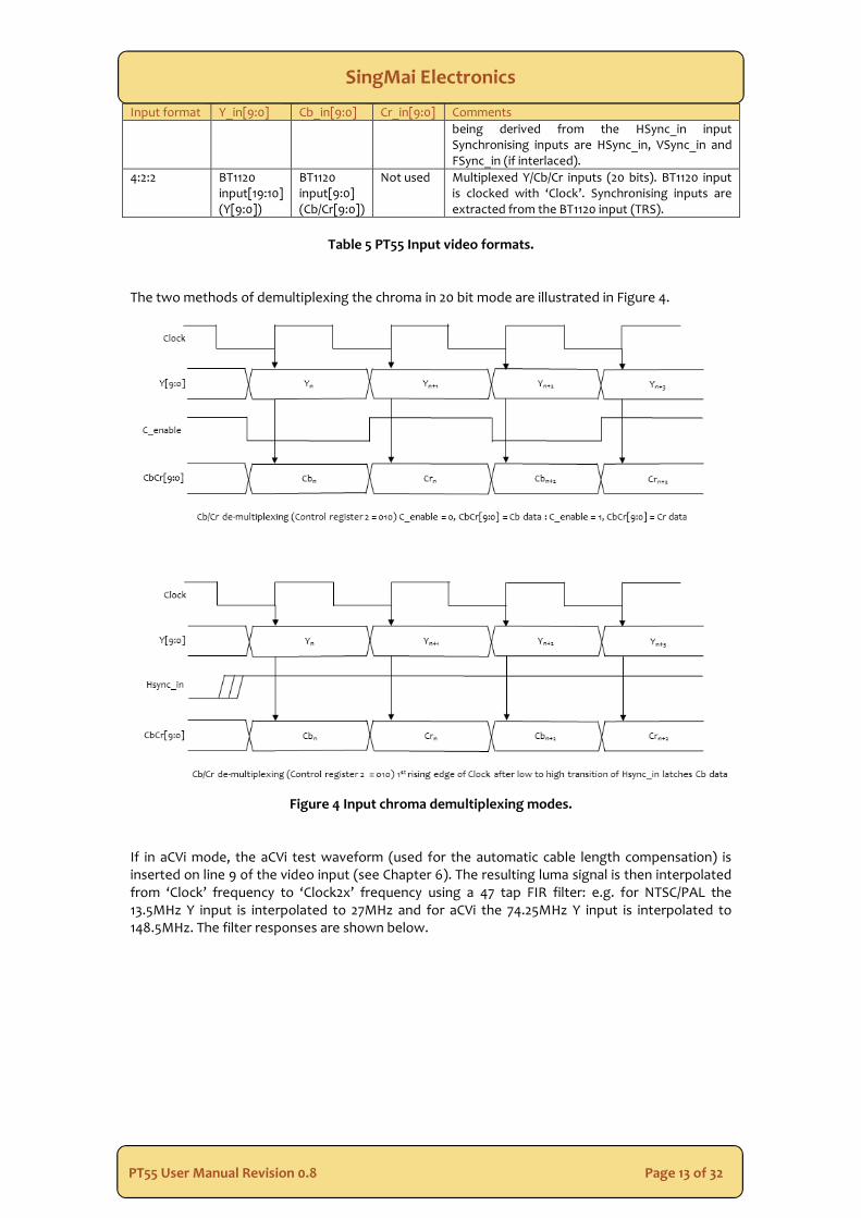
The PT55 can accept 3 different formats of video input as described in Table 5. Selection of theinput format is made using Control register 2, bits [2:0].
Input format Y_in[9:0] Cb_in[9:0] Cr_in[9:0] Comments
4:4:4/4:2:2 Y input Cb input Cr input Separate Y/Cb/Cr inputs (30 bits). Y is clocked with‘Clock’, Cb/Cr are clocked with ‘Clock’ in 4:4:4mode or with ‘Clock’ if ‘C_enable’ is ‘1’ in 4:2:2mode. Synchronising inputs are HSync_in,VSync_in and FSync_in (if interlaced).
4:2:2 Y input Cb/Cr input Not used Separate Y and multiplexed Cb/Cr inputs (20 bits).Y is clocked with ‘Clock’, Cb/Cr are clocked with‘Clock’ with either ‘C_enable’ signaling which is Cb(= ‘0’) or Cr (= ‘1’) or the demultiplexing signal
SingMai Electronics
PT55 User Manual Revision 0.8 Page 13 of 32
Input format Y_in[9:0] Cb_in[9:0] Cr_in[9:0] Comments
being derived from the HSync_in inputSynchronising inputs are HSync_in, VSync_in andFSync_in (if interlaced).
4:2:2 BT1120input[19:10](Y[9:0])
BT1120input[9:0](Cb/Cr[9:0])
Not used Multiplexed Y/Cb/Cr inputs (20 bits). BT1120 inputis clocked with ‘Clock’. Synchronising inputs areextracted from the BT1120 input (TRS).
Table 5 PT55 Input video formats.
The two methods of demultiplexing the chroma in 20 bit mode are illustrated in Figure 4.
Figure 4 Input chroma demultiplexing modes.
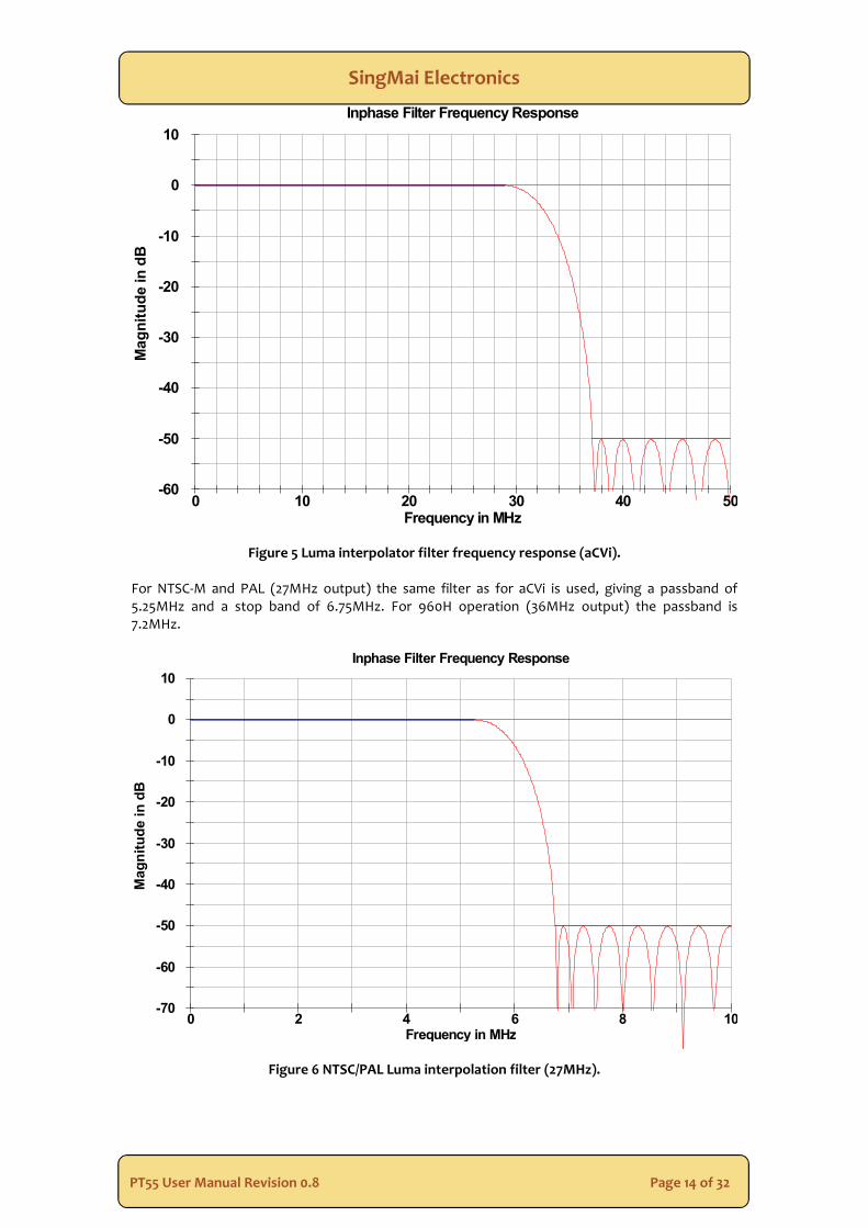
If in aCVi mode, the aCVi test waveform (used for the automatic cable length compensation) isinserted on line 9 of the video input (see Chapter 6). The resulting luma signal is then interpolatedfrom ‘Clock’ frequency to ‘Clock2x’ frequency using a 47 tap FIR filter: e.g. for NTSC/PAL the13.5MHz Y input is interpolated to 27MHz and for aCVi the 74.25MHz Y input is interpolated to148.5MHz. The filter responses are shown below.
SingMai Electronics
PT55 User Manual Revision 0.8 Page 14 of 32
Figure 5 Luma interpolator filter frequency response (aCVi).
For NTSC-M and PAL (27MHz output) the same filter as for aCVi is used, giving a passband of5.25MHz and a stop band of 6.75MHz. For 960H operation (36MHz output) the passband is7.2MHz.
Figure 6 NTSC/PAL Luma interpolation filter (27MHz).
Inphase Filter Frequency Response
Frequency in MHz
Ma
gn
itu
de
ind
B
0 10 20 30 40 50-60
-50
-40
-30
-20
-10
0
10
Inphase Filter Frequency Response
Frequency in MHz
Mag
nit
ud
ein
dB
0 2 4 6 8 10-70
-60
-50
-40
-30
-20
-10
0
10
SingMai Electronics
PT55 User Manual Revision 0.8 Page 15 of 32
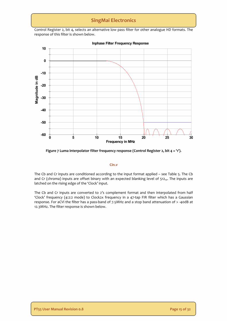
Control Register 2, bit 4, selects an alternative low pass filter for other analogue HD formats. Theresponse of this filter is shown below.
Figure 7 Luma interpolator filter frequency response (Control Register 2, bit 4 = '1').
Cin.v
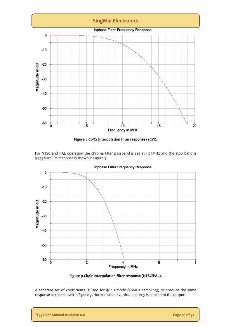
The Cb and Cr inputs are conditioned according to the input format applied – see Table 5. The Cband Cr (chroma) inputs are offset binary with an expected blanking level of 51210. The inputs arelatched on the rising edge of the ‘Clock’ input.
The Cb and Cr inputs are converted to 2’s complement format and then interpolated from half‘Clock’ frequency (4:2:2 mode) to Clock2x frequency in a 47-tap FIR filter which has a Gaussianresponse. For aCVi the filter has a pass-band of 7.5MHz and a stop band attenuation of > -40dB at12.3MHz. The filter response is shown below.
Inphase Filter Frequency Response
Frequency in MHz
Ma
gn
itu
de
ind
B
0 5 10 15 20 25 30-60
-50
-40
-30
-20
-10
0
10
SingMai Electronics
PT55 User Manual Revision 0.8 Page 16 of 32
Figure 8 Cb/Cr Interpolation filter response (aCVi).
For NTSC and PAL operation the chroma filter passband is set at 1.07MHz and the stop band is3.375MHz - its response is shown in Figure 9.
Figure 9 Cb/Cr Interpolation filter response (NTSC/PAL).
A separate set of coefficients is used for 960H mode (36MHz sampling), to produce the sameresponse as that shown in Figure 9. Horizontal and vertical blanking is applied to the output.
Inphase Filter Frequency Response
Frequency in MHz
Mag
nit
ud
ein
dB
0 5 10 15 20-60
-50
-40
-30
-20
-10
0
Inphase Filter Frequency Response
Frequency in MHz
Mag
nit
ud
ein
dB
0 2 4 6 8-60
-50
-40
-30
-20
-10
0
SingMai Electronics
PT55 User Manual Revision 0.8 Page 17 of 32
SPG.v
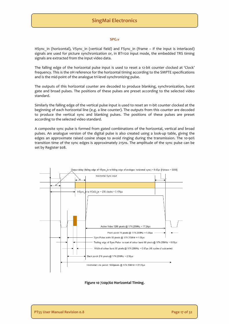
HSync_in (horizontal), VSync_in (vertical field) and FSync_in (frame – if the input is interlaced)signals are used for picture synchronization or, in BT1120 input mode, the embedded TRS timingsignals are extracted from the input video data.
The falling edge of the horizontal pulse input is used to reset a 12-bit counter clocked at ‘Clock’frequency. This is the 0H reference for the horizontal timing according to the SMPTE specificationsand is the mid-point of the analogue tri-level synchronizing pulse.
The outputs of this horizontal counter are decoded to produce blanking, synchronization, burstgate and broad pulses. The positions of these pulses are preset according to the selected videostandard.
Similarly the falling edge of the vertical pulse input is used to reset an 11-bit counter clocked at thebeginning of each horizontal line (e.g. a line counter). The outputs from this counter are decodedto produce the vertical sync and blanking pulses. The positions of these pulses are presetaccording to the selected video standard.
A composite sync pulse is formed from gated combinations of the horizontal, vertical and broadpulses. An analogue version of the digital pulse is also created using a look-up table, giving theedges an approximate raised cosine shape to avoid ringing during the transmission. The 10-90%transition time of the sync edges is approximately 215ns. The amplitude of the sync pulse can beset by Register $08.
Figure 10 720p/60 Horizontal Timing.
SingMai Electronics
PT55 User Manual Revision 0.8 Page 18 of 32
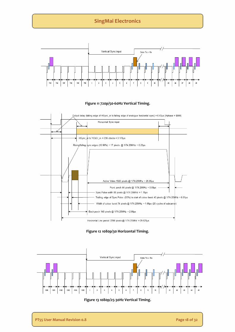
Figure 11 720p/50-60Hz Vertical Timing.
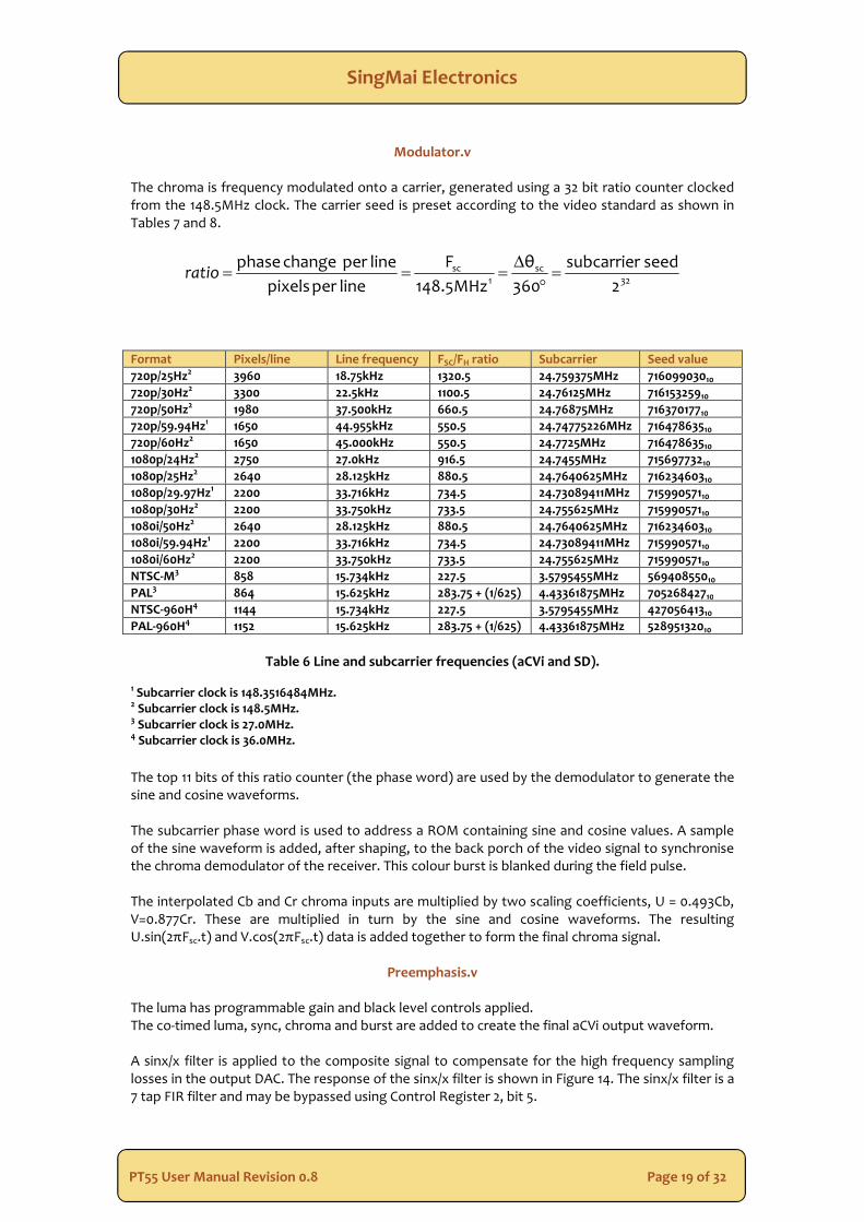
Figure 12 1080p/30 Horizontal Timing.
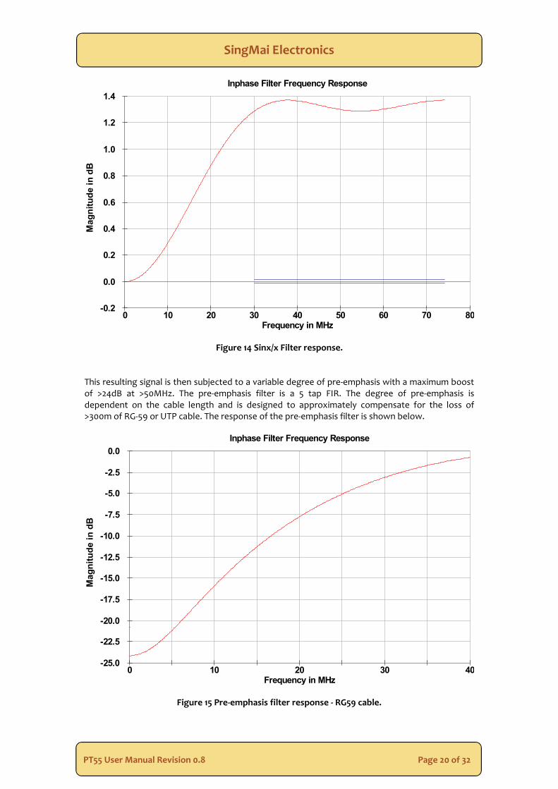
Figure 13 1080p/25-30Hz Vertical Timing.
SingMai Electronics
PT55 User Manual Revision 0.8 Page 19 of 32
Modulator.v
The chroma is frequency modulated onto a carrier, generated using a 32 bit ratio counter clockedfrom the 148.5MHz clock. The carrier seed is preset according to the video standard as shown inTables 7 and 8.
32sc
1sc
2
seedsubcarrier
360
θ
148.5MHz
F
lineperpixels
lineperchangephase
ratio
Format Pixels/line Line frequency FSC/FH ratio Subcarrier Seed value
720p/25Hz2 3960 18.75kHz 1320.5 24.759375MHz 71609903010
720p/30Hz2 3300 22.5kHz 1100.5 24.76125MHz 71615325910
720p/50Hz2 1980 37.500kHz 660.5 24.76875MHz 71637017710
720p/59.94Hz1 1650 44.955kHz 550.5 24.74775226MHz 71647863510
720p/60Hz2 1650 45.000kHz 550.5 24.7725MHz 71647863510
1080p/24Hz2 2750 27.0kHz 916.5 24.7455MHz 71569773210
1080p/25Hz2 2640 28.125kHz 880.5 24.7640625MHz 71623460310
1080p/29.97Hz1 2200 33.716kHz 734.5 24.73089411MHz 71599057110
1080p/30Hz2 2200 33.750kHz 733.5 24.755625MHz 71599057110
1080i/50Hz2 2640 28.125kHz 880.5 24.7640625MHz 71623460310
1080i/59.94Hz1 2200 33.716kHz 734.5 24.73089411MHz 71599057110
1080i/60Hz2 2200 33.750kHz 733.5 24.755625MHz 71599057110
NTSC-M3 858 15.734kHz 227.5 3.5795455MHz 56940855010
PAL3 864 15.625kHz 283.75 + (1/625) 4.43361875MHz 70526842710
NTSC-960H4 1144 15.734kHz 227.5 3.5795455MHz 42705641310
PAL-960H4 1152 15.625kHz 283.75 + (1/625) 4.43361875MHz 52895132010
Table 6 Line and subcarrier frequencies (aCVi and SD).
1 Subcarrier clock is 148.3516484MHz.2 Subcarrier clock is 148.5MHz.3 Subcarrier clock is 27.0MHz.4 Subcarrier clock is 36.0MHz.
The top 11 bits of this ratio counter (the phase word) are used by the demodulator to generate thesine and cosine waveforms.
The subcarrier phase word is used to address a ROM containing sine and cosine values. A sampleof the sine waveform is added, after shaping, to the back porch of the video signal to synchronisethe chroma demodulator of the receiver. This colour burst is blanked during the field pulse.
The interpolated Cb and Cr chroma inputs are multiplied by two scaling coefficients, U = 0.493Cb,V=0.877Cr. These are multiplied in turn by the sine and cosine waveforms. The resultingU.sin(2πFsc.t) and V.cos(2πFsc.t) data is added together to form the final chroma signal.
Preemphasis.v
The luma has programmable gain and black level controls applied.The co-timed luma, sync, chroma and burst are added to create the final aCVi output waveform.
A sinx/x filter is applied to the composite signal to compensate for the high frequency samplinglosses in the output DAC. The response of the sinx/x filter is shown in Figure 14. The sinx/x filter is a7 tap FIR filter and may be bypassed using Control Register 2, bit 5.
SingMai Electronics
PT55 User Manual Revision 0.8 Page 20 of 32
Figure 14 Sinx/x Filter response.
This resulting signal is then subjected to a variable degree of pre-emphasis with a maximum boostof >24dB at >50MHz. The pre-emphasis filter is a 5 tap FIR. The degree of pre-emphasis isdependent on the cable length and is designed to approximately compensate for the loss of>300m of RG-59 or UTP cable. The response of the pre-emphasis filter is shown below.
Figure 15 Pre-emphasis filter response - RG59 cable.
Inphase Filter Frequency Response
Frequency in MHz
Mag
nit
ud
ein
dB
0 10 20 30 40 50 60 70 80-0.2
0.0
0.2
0.4
0.6
0.8
1.0
1.2
1.4
Inphase Filter Frequency Response
Frequency in MHz
Mag
nit
ud
ein
dB
0 10 20 30 40-25.0
-22.5
-20.0
-17.5
-15.0
-12.5
-10.0
-7.5
-5.0
-2.5
0.0
SingMai Electronics
PT55 User Manual Revision 0.8 Page 21 of 32
The resulting digital aCVi encoded output should be input to a digital to analogue converter (DAC)and then buffered to drive the cable.
Figure 16 aCVi output, 30MHz sweep (Pre-emphasis = minimum).
Figure 17 aCVi output, 30MHz sweep (Pre-emphasis = maximum).
SingMai Electronics
PT55 User Manual Revision 0.8 Page 22 of 32
6. aCVi Cable Compensation
The following description only applies to aCVi video.
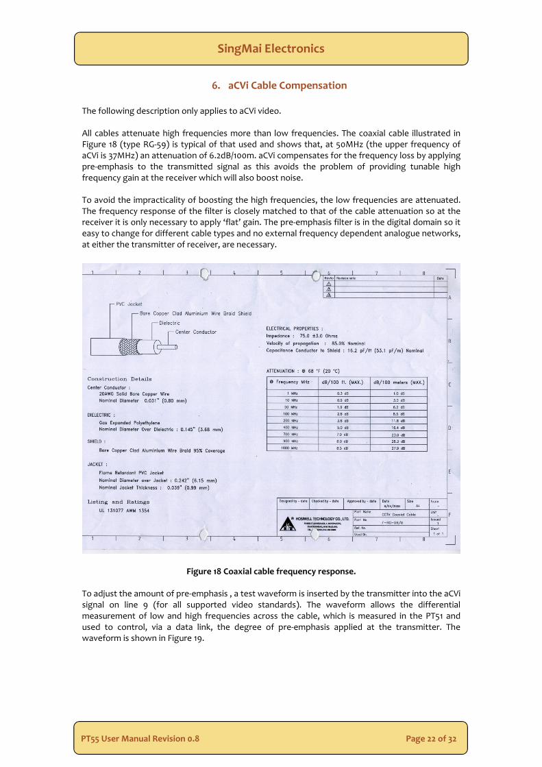
All cables attenuate high frequencies more than low frequencies. The coaxial cable illustrated inFigure 18 (type RG-59) is typical of that used and shows that, at 50MHz (the upper frequency ofaCVi is 37MHz) an attenuation of 6.2dB/100m. aCVi compensates for the frequency loss by applyingpre-emphasis to the transmitted signal as this avoids the problem of providing tunable highfrequency gain at the receiver which will also boost noise.
To avoid the impracticality of boosting the high frequencies, the low frequencies are attenuated.The frequency response of the filter is closely matched to that of the cable attenuation so at thereceiver it is only necessary to apply ‘flat’ gain. The pre-emphasis filter is in the digital domain so iteasy to change for different cable types and no external frequency dependent analogue networks,at either the transmitter of receiver, are necessary.
Figure 18 Coaxial cable frequency response.
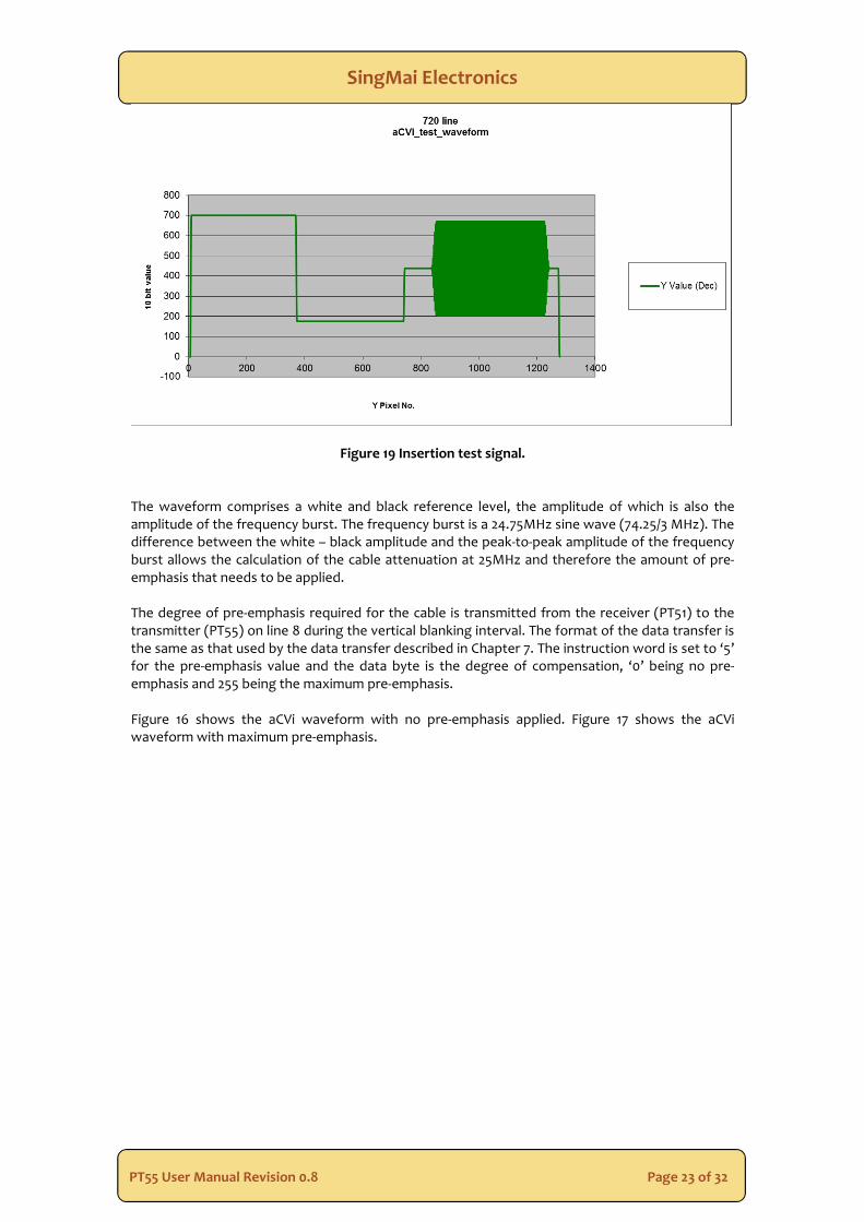
To adjust the amount of pre-emphasis , a test waveform is inserted by the transmitter into the aCVisignal on line 9 (for all supported video standards). The waveform allows the differentialmeasurement of low and high frequencies across the cable, which is measured in the PT51 andused to control, via a data link, the degree of pre-emphasis applied at the transmitter. Thewaveform is shown in Figure 19.
SingMai Electronics
PT55 User Manual Revision 0.8 Page 23 of 32
Figure 19 Insertion test signal.
The waveform comprises a white and black reference level, the amplitude of which is also theamplitude of the frequency burst. The frequency burst is a 24.75MHz sine wave (74.25/3 MHz). Thedifference between the white – black amplitude and the peak-to-peak amplitude of the frequencyburst allows the calculation of the cable attenuation at 25MHz and therefore the amount of pre-emphasis that needs to be applied.
The degree of pre-emphasis required for the cable is transmitted from the receiver (PT51) to thetransmitter (PT55) on line 8 during the vertical blanking interval. The format of the data transfer isthe same as that used by the data transfer described in Chapter 7. The instruction word is set to ‘5’for the pre-emphasis value and the data byte is the degree of compensation, ‘0’ being no pre-emphasis and 255 being the maximum pre-emphasis.
Figure 16 shows the aCVi waveform with no pre-emphasis applied. Figure 17 shows the aCViwaveform with maximum pre-emphasis.
SingMai Electronics
PT55 User Manual Revision 0.8 Page 24 of 32
7. Data Transfers
The following description only applies to aCVi video.
The aCVi interface supports the bi-directional transfer of data between receiver and transmitter.The data is transmitted during the vertical blanking interval (Line 12 transmits from receiver totransmitter and Line 13 from transmitter to receiver).
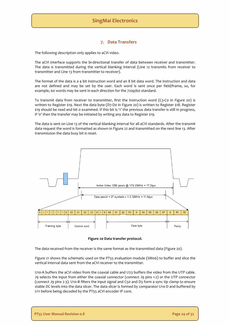
The format of the data is a 4 bit instruction word and an 8 bit data word. The instruction and dataare not defined and may be set by the user. Each word is sent once per field/frame, so, forexample, 60 words may be sent in each direction for the 720p/60 standard.
To transmit data from receiver to transmitter, first the instruction word (C3-C0 in Figure 20) iswritten to Register $19. Next the data byte (D7-D0 in Figure 20) is written to Register $18. Register$19 should be read and bit 0 examined. If this bit is ‘1’ the previous data transfer is still in progress,if ‘0’ then the transfer may be initiated by writing any data to Register $19.
The data is sent on Line 13 of the vertical blanking interval for all aCVi standards. After the transmitdata request the word is formatted as shown in Figure 22 and transmitted on the next line 13. Aftertransmission the data busy bit is reset.
Figure 20 Data transfer protocol.
The data received from the receiver is the same format as the transmitted data (Figure 20).
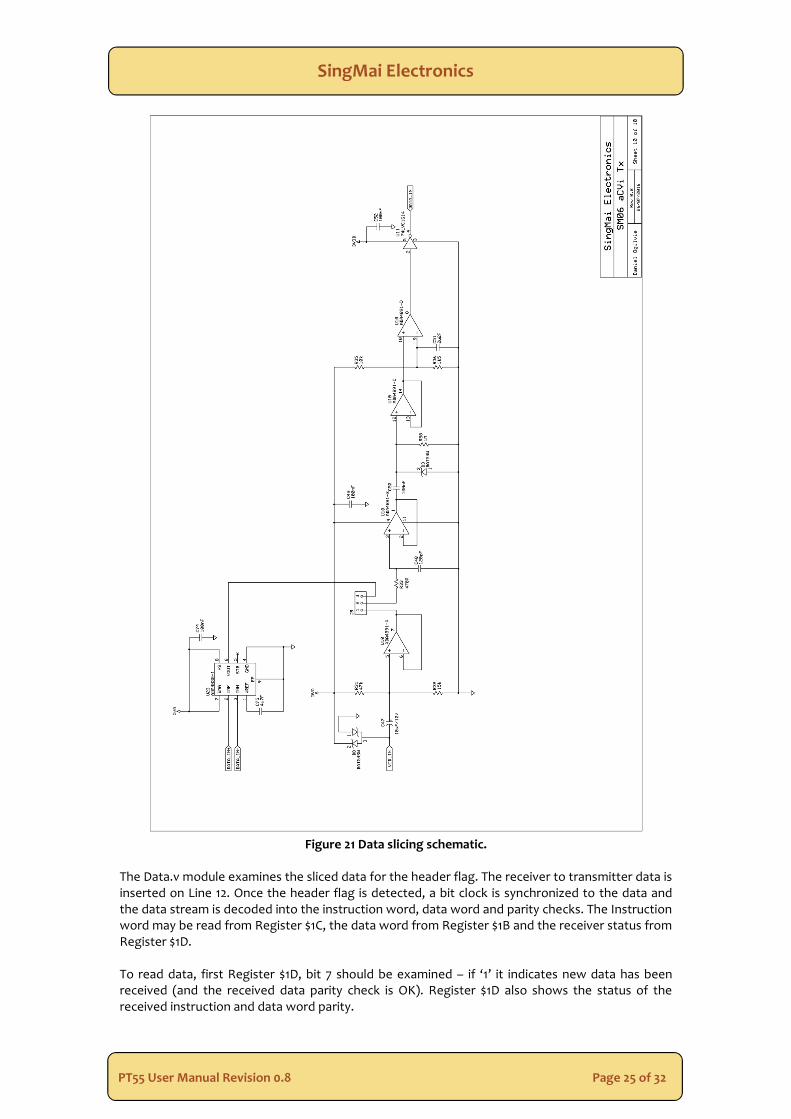
Figure 21 shows the schematic used on the PT55 evaluation module (SM06) to buffer and slice thevertical interval data sent from the aCVi receiver to the transmitter.
U10-A buffers the aCVi video from the coaxial cable and U23 buffers the video from the UTP cable.J9 selects the input from either the coaxial connector (connect J9 pins 1-2) or the UTP connector(connect J9 pins 2-3). U10-B filters the input signal and C50 and D3 form a sync tip clamp to ensurestable DC levels into the data slicer. The data slicer is formed by comparator U10-D and buffered byU11 before being decoded by the PT55 aCVi encoder IP core.
SingMai Electronics
PT55 User Manual Revision 0.8 Page 25 of 32
Figure 21 Data slicing schematic.
The Data.v module examines the sliced data for the header flag. The receiver to transmitter data isinserted on Line 12. Once the header flag is detected, a bit clock is synchronized to the data andthe data stream is decoded into the instruction word, data word and parity checks. The Instructionword may be read from Register $1C, the data word from Register $1B and the receiver status fromRegister $1D.
To read data, first Register $1D, bit 7 should be examined – if ‘1’ it indicates new data has beenreceived (and the received data parity check is OK). Register $1D also shows the status of thereceived instruction and data word parity.
SingMai Electronics
PT55 User Manual Revision 0.8 Page 26 of 32
Next the received instruction word should be read from Register $1C, and then the received dataword from Register $1B. When Register $1B is read the new data flag (Register $1D bit 7) is reset.When the new data bit is set new received data will not be latched, preventing corruption ofreceived data, but also possibly missing transmitted data if the data is not read often enough.
SingMai Electronics
PT55 User Manual Revision 0.8 Page 27 of 32
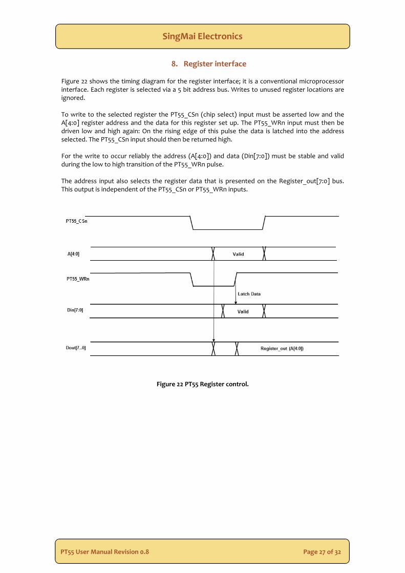
8. Register interface
Figure 22 shows the timing diagram for the register interface; it is a conventional microprocessorinterface. Each register is selected via a 5 bit address bus. Writes to unused register locations areignored.
To write to the selected register the PT55_CSn (chip select) input must be asserted low and theA[4:0] register address and the data for this register set up. The PT55_WRn input must then bedriven low and high again: On the rising edge of this pulse the data is latched into the addressselected. The PT55_CSn input should then be returned high.
For the write to occur reliably the address (A[4:0]) and data (Din[7:0]) must be stable and validduring the low to high transition of the PT55_WRn pulse.
The address input also selects the register data that is presented on the Register_out[7:0] bus.This output is independent of the PT55_CSn or PT55_WRn inputs.
Figure 22 PT55 Register control.
SingMai Electronics
PT55 User Manual Revision 0.8 Page 28 of 32
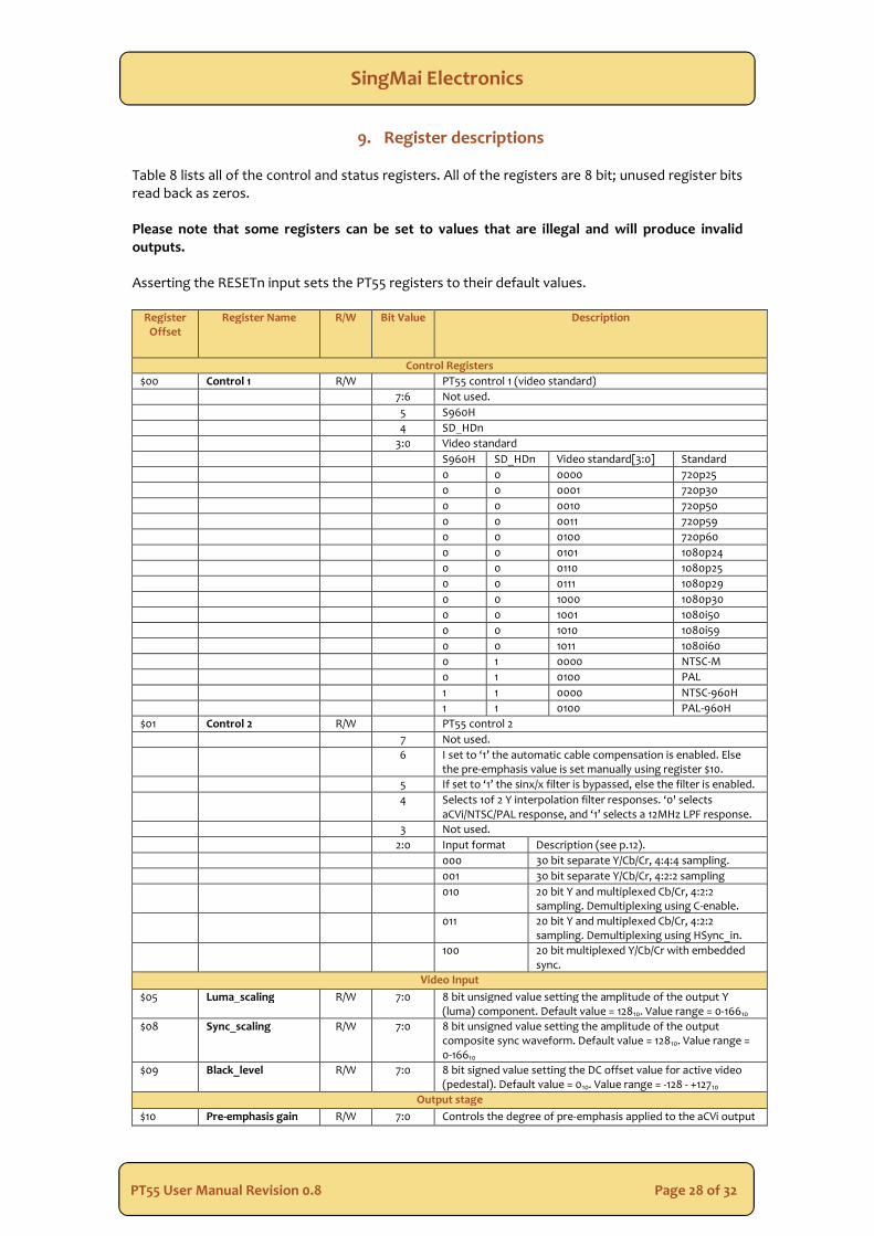
9. Register descriptions
Table 8 lists all of the control and status registers. All of the registers are 8 bit; unused register bitsread back as zeros.
Please note that some registers can be set to values that are illegal and will produce invalidoutputs.
Asserting the RESETn input sets the PT55 registers to their default values.
RegisterOffset
Register Name R/W Bit Value Description
Control Registers
$00 Control 1 R/W PT55 control 1 (video standard)
7:6 Not used.
5 S960H
4 SD_HDn
3:0 Video standard
S960H SD_HDn Video standard[3:0] Standard
0 0 0000 720p25
0 0 0001 720p30
0 0 0010 720p50
0 0 0011 720p59
0 0 0100 720p60
0 0 0101 1080p24
0 0 0110 1080p25
0 0 0111 1080p29
0 0 1000 1080p30
0 0 1001 1080i50
0 0 1010 1080i59
0 0 1011 1080i60
0 1 0000 NTSC-M
0 1 0100 PAL
1 1 0000 NTSC-960H
1 1 0100 PAL-960H
$01 Control 2 R/W PT55 control 2
7 Not used.
6 I set to ‘1’ the automatic cable compensation is enabled. Elsethe pre-emphasis value is set manually using register $10.
5 If set to ‘1’ the sinx/x filter is bypassed, else the filter is enabled.
4 Selects 1of 2 Y interpolation filter responses. ‘0' selectsaCVi/NTSC/PAL response, and ‘1’ selects a 12MHz LPF response.
3 Not used.
2:0 Input format Description (see p.12).
000 30 bit separate Y/Cb/Cr, 4:4:4 sampling.
001 30 bit separate Y/Cb/Cr, 4:2:2 sampling
010 20 bit Y and multiplexed Cb/Cr, 4:2:2sampling. Demultiplexing using C-enable.
011 20 bit Y and multiplexed Cb/Cr, 4:2:2sampling. Demultiplexing using HSync_in.
100 20 bit multiplexed Y/Cb/Cr with embeddedsync.
Video Input
$05 Luma_scaling R/W 7:0 8 bit unsigned value setting the amplitude of the output Y(luma) component. Default value = 12810. Value range = 0-16610
$08 Sync_scaling R/W 7:0 8 bit unsigned value setting the amplitude of the outputcomposite sync waveform. Default value = 12810. Value range =0-16610
$09 Black_level R/W 7:0 8 bit signed value setting the DC offset value for active video(pedestal). Default value = 010. Value range = -128 - +12710
Output stage
$10 Pre-emphasis gain R/W 7:0 Controls the degree of pre-emphasis applied to the aCVi output
SingMai Electronics
PT55 User Manual Revision 0.8 Page 29 of 32
RegisterOffset
Register Name R/W Bit Value Description
(in manual pre-emphasis mode – Register $01 bit 6 = 0). Default= 0 = no pre-emphasis. Maximum pre-emphasis = 25510.
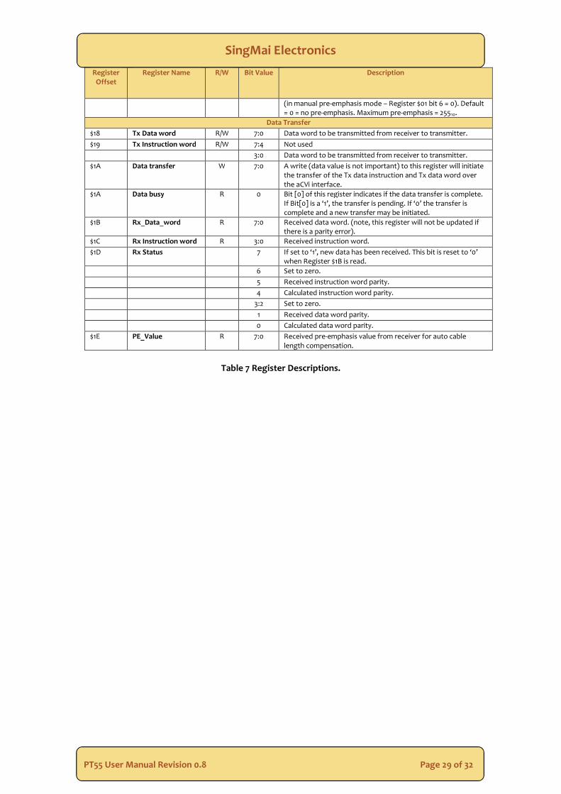
Data Transfer
$18 Tx Data word R/W 7:0 Data word to be transmitted from receiver to transmitter.
$19 Tx Instruction word R/W 7:4 Not used
3:0 Data word to be transmitted from receiver to transmitter.
$1A Data transfer W 7:0 A write (data value is not important) to this register will initiatethe transfer of the Tx data instruction and Tx data word overthe aCVi interface.
$1A Data busy R 0 Bit [0] of this register indicates if the data transfer is complete.If Bit[0] is a ‘1’, the transfer is pending. If ‘0’ the transfer iscomplete and a new transfer may be initiated.
$1B Rx_Data_word R 7:0 Received data word. (note, this register will not be updated ifthere is a parity error).
$1C Rx Instruction word R 3:0 Received instruction word.
$1D Rx Status 7 If set to ‘1’, new data has been received. This bit is reset to ‘0’when Register $1B is read.
6 Set to zero.
5 Received instruction word parity.
4 Calculated instruction word parity.
3:2 Set to zero.
1 Received data word parity.
0 Calculated data word parity.
$1E PE_Value R 7:0 Received pre-emphasis value from receiver for auto cablelength compensation.
Table 7 Register Descriptions.
SingMai Electronics
PT55 User Manual Revision 0.8 Page 30 of 32
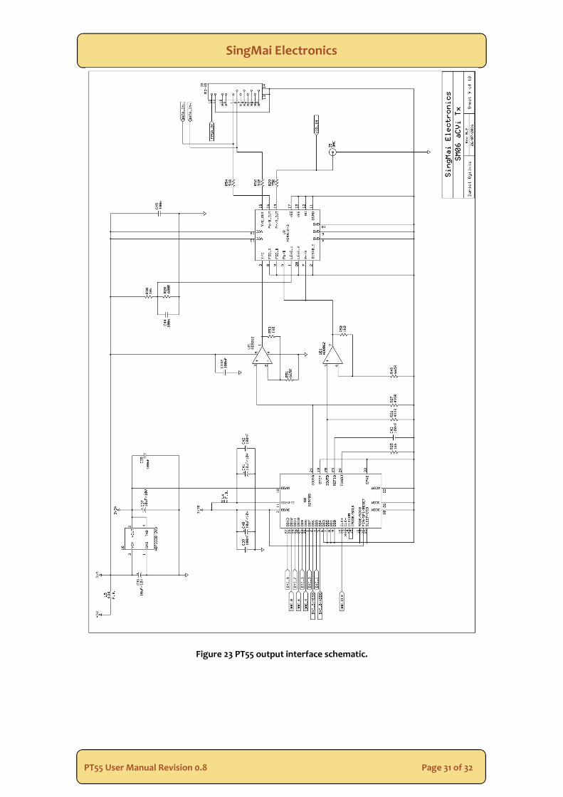
10. Output Interface
The output of the aCVi encoder is 10-bit, straight binary, video data at 148.5MHz.
This has to be converted to analogue using a digital to analogue converter. On the evaluationboard (SM06 revision 0.2) an Analog Devices 10-bit DAC, the AD9705, is used for this purpose.
The FPGA also provides a 148.5MHz clock for the DAC.
The differential analogue outputs from the DAC (1.0V pk-pk) are then amplified by U21 and filtered(U9) to remove clock noise and driven through a cable impedance matching series resistor to thecoaxial or twisted-pair cable.
The schematics for this are shown in Figure 23.
SingMai Electronics
PT55 User Manual Revision 0.8 Page 31 of 32
Figure 23 PT55 output interface schematic.

SingMai Electronics
PT55 User Manual Revision 0.8 Page 32 of 32
11. Altera Encrypted files
For evaluation of the PT55 using an Altera FPGA, SingMai can provide encrypted Verilog files,specific to the computer you will compile the design on. For us to provide these files SingMaineeds to have the NIC number of the computer you will be running Quartus on.
The encrypted files name have a similar naming to the original files – see Table 9. The files may becompiled and simulated exactly as the original files, the only difference is they cannot be viewed.
Original module name Encrypted module name
aCVi_encoder.v aCVi_encoder_enc.v
aCVI_Register_control.v aCVI_Register_control_enc.v
aCVi_Cin.v aCVi_Cin_enc.v
aCVi_Yin.v aCVi_Yin_enc.v
aCVI_Tx_SPG.v aCVI_Tx_SPG_enc.v
aCVi_Modulator.v aCVi_Modulator_enc.v
aCVi_Preemphasis.v aCVi_Preemphasis_enc.v
aCVi_data.v aCVi_data_enc.v
Tx_SinCos_ROM.v Tx_SinCos_ROM_enc.v
aCVI_test_waveform.v aCVI_test_waveform _enc.v
Table 8 Encrypted file naming.
First copy the files across into your main project directory.
It is necessary to add the design file to your project which is done by clicking on ‘Project’ and then‘Add/Remove Files in Project…’ (within Quartus II). See Figure
Next we need to tell Quartus where to find the associated license file.
Within Quartus click on ‘Tools’ and then ‘License Setup’. Click on the browse button to the right ofthe ‘License file’ dialog box and point to the PT55_license.dat file.
The files should then be able to be compiled and simulated.
The license file is unique to you but allows unlimited use of the PT55 across the whole family ofAltera programmable devices. It will usually expire 2 months after the date of issue. Please contactSingMai if you need an extension of this.


![Company Overview March 2015.ppt [Read-Only] · Design and manufacture of products for the video, imaging and broadcast markets Established in September 2007. SingMai (·É Ä®¤)](https://img.pdfslide.us/doc/110x75/5adc875e7f8b9a4a268c35a8/company-overview-march-2015ppt-read-only-and-manufacture-of-products-for-the.jpg)