Embed Size (px)
Citation preview
30V, 1.2A Step-down High Brightness LED Driver with 5000:1 Dimming
China Resources Powtech (Shanghai) Limited WWW.CRPOWTECH.COM Page 1 PT4115_DS Rev EN_2.8
PT4115
GENERAL DESCRIPTION
The PT4115 is a continuous conduction mode inductive step-down converter, designed for driving single or multiple series connected LED efficiently from a voltage source higher than the total LED chain voltage. The device operates from an input supply between 6V and 30V and provides an externally adjustable output current of up to 1.2A. Depending upon the supply voltage and external components, the PT4115can provide more than 30 watts of output power. The PT4115 includes the power switch and a high-side output current sensing circuit, which uses an external resistor to set the nominal average output current, and a dedicated DIM input accepts either a DC voltage or a wide range of pulsed dimming. Applying a voltage of 0.3V or lower to the DIM pin turns the output off and switches the device into a low current standby state. The PT4115 is available in SOT89-5 and ESOP8 packages.
FEATURES Simple low parts count Wide input voltage range: 6V to 30V Up to 1.2A output current Single pin on/off and brightness control using DC
voltage or PWM Up to 1MHz switching frequency Typical 5% output current accuracy Inherent open-circuit LED protection High efficiency (up to 97%) High-Side Current Sense Hysteretic Control: No Compensatio Adjustable Constant LED Current ESOP8 package for large output power application
APPLICATIONS Low voltage halogen replacement LEDs Automotive lighting Low voltage industrial lighting LED back-up lighting Illuminated signs SELV lighting LCD TV backlighting
ORDERING INFORMATION
PACKAGE TEMPERATURE RANGE
ORDERING PART NUMBER
TRANSPORT MEDIA MARKING
SOT89-5 -40 oC to 85 oC PT4115-89E Tape and Reel 1000 units
PT4115 xxxxxX
ESOP8 -40 oC to 85 oC PT4115-SOH Tape and Reel 2500 units
PT4115 xxxxxX
Note:
TYPICAL APPLICATION CIRCUIT
xxxxxXAssembly Factory Code
Lot Number
30V, 1.2A Step-down High Brightness LED Driver with 5000:1 Dimming
China Resources Powtech (Shanghai) Limited WWW.CRPOWTECH.COM Page 2 PT4115_DS Rev EN_2.8
PT4115
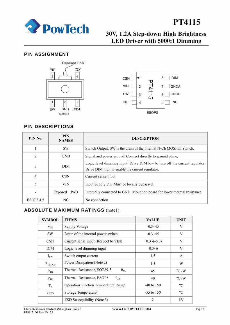
PIN ASSIGNMENT
PIN DESCRIPTIONS
PIN No. PIN NAMES DESCRIPTION
1 SW Switch Output. SW is the drain of the internal N-Ch MOSFET switch.
2 GND Signal and power ground. Connect directly to ground plane.
3 DIM Logic level dimming input. Drive DIM low to turn off the current regulator. Drive DIM high to enable the current regulator.
4 CSN Current sense input
5 VIN Input Supply Pin. Must be locally bypassed.
- Exposed PAD Internally connected to GND. Mount on board for lower thermal resistance.
ESOP8 4,5 NC No connection
ABSOLUTE MAXIMUM RATINGS (note1)
SYMBOL ITEMS VALUE UNIT
VIN Supply Voltage -0.3~45 V
SW Drain of the internal power switch -0.3~45 V
CSN Current sense input (Respect to VIN) +0.3~(-6.0) V
DIM Logic level dimming input -0.3~6 V
ISW Switch output current 1.5 A
PDMAX Power Dissipation (Note 2) 1.5 W
PTR Thermal Resistance, SOT89-5 θJA 45 oC /W
PTR Thermal Resistance, ESOP8 θJA 40 oC /W
TJ Operation Junction Temperature Range -40 to 150 oC
TSTG Storage Temperature -55 to 150 oC
ESD Susceptibility (Note 3) 2 kV
1
2
3
4 5
6
7
8PT
4115CSN
VIN
SW
NC NC
GNDP
GNDA
DIM
ESOP8
30V, 1.2A Step-down High Brightness LED Driver with 5000:1 Dimming
China Resources Powtech (Shanghai) Limited WWW.CRPOWTECH.COM Page 3 PT4115_DS Rev EN_2.8
PT4115
RECOMMENDED OPERATING RANGE
SYMBOL ITEMS VALUE UNIT
VIN VDD Supply Voltage 6 ~ 30 V
TOPT Operating Temperature -40 to +85 oC
Note 1: Absolute Maximum Ratings indicate limits beyond which damage to the device may occur. Recommended Operating Range indicates conditions for which the device is functional, but do not guarantee specific performance limits. Electrical Characteristics state DC and AC electrical specifications under particular test conditions which guarantee specific performance limits. This assumes that the device is within the Operating Range. Specifications are not guaranteed for parameters where no limit is given, however, the typical value is a good indication of device performance. Note 2: The maximum power dissipation must be derated at elevated temperatures and is dictated by TJMAX, θJA, and the ambient temperature TA. The maximum allowable power dissipation is PDMAX = (TJMAX - TA)/ θJA or the number given in Absolute Maximum Ratings, whichever is lower. Note 3: Human body model, 100pF discharged through a 1.5kΩ resistor.
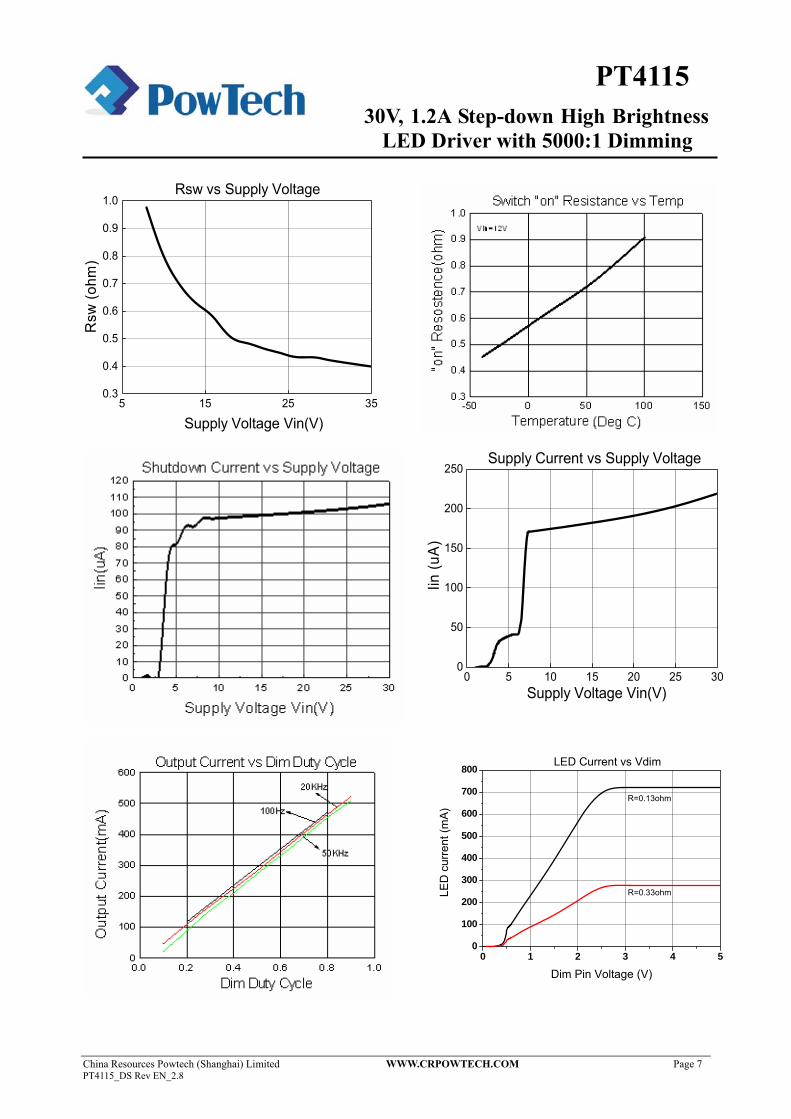
ELECTRICAL CHARACTERISTICS (Note 4, 5)
The following specifications apply for VIN=12V, TA=25 oC, unless specified otherwise.
SYMBOL ITEMS CONDITIONS Min. Typ. Max. UNITVIN Input Voltage 6 30 V
VUVLO Under voltage lock out VIN falling 5.1 V VUVLO, HYS UVLO hysterisis VIN rising 500 mV
FSW Max. Switching Frequency 1 MHz
Current Sense A type 95 98 101 mV
VCSN Mean current sense threshold voltage
VIN-VCSN B type 99 102 105 mV
VCSN_hys Sense threshold hysteresis ±15 % ICSN CSN Pin Input Current VIN-VCSN=50mV 8 µA
Operating Current
IOFF Quiescent supply current with output off
VDIM<0.3V 95 µA
DIM Input VDIM Internal supply voltage DIM floating 5 V
VDIM_H DIM input voltage High 2.5 V VDIM_L DIM input voltage Low 0.3 V
VDIM_DC DC brightness control 0.5 2.5 V fDIM Max. DIM Frequency fOSC=500kHz 50 kHz
Duty cycle range of low frequency dimming
fDIM =100Hz 0.02% 1 DPWM_LF
Brightness control range 5000:1
30V, 1.2A Step-down High Brightness LED Driver with 5000:1 Dimming
China Resources Powtech (Shanghai) Limited WWW.CRPOWTECH.COM Page 4 PT4115_DS Rev EN_2.8
PT4115
ELECTRICAL CHARACTERISTICS (Continued) (Note 4, 5)
SYMBOL ITEMS CONDITIONS Min. Typ. Max. UNITDIM Input
Duty cycle range of high frequency dimming
fDIM =20KHz 4% 1 DPWM_HF
Brightness control range 25:1 RDIM DIM pull up resistor to Internal
supply voltage 200 KΩ
IDIM_L DIM input leakage low VDIM = 0 25 uA
Output Switch VIN=12V 0.6 RSW SW On Resistance VIN=24V 0.4
Ω
ISWmean Continuous SW Current 1.2 A ILEAK SW Leakage Current 0.5 5 µA
Thermal Shutdown TSD Thermal Shutdown Threshold 160
TSD-hys Thermal Shutdown hysteresis 20
Note 4: Typical parameters are measured at 25˚C and represent the parametric norm. Note 5: Datasheet min/max specification limits are guaranteed by design, test, or statistical analysis.
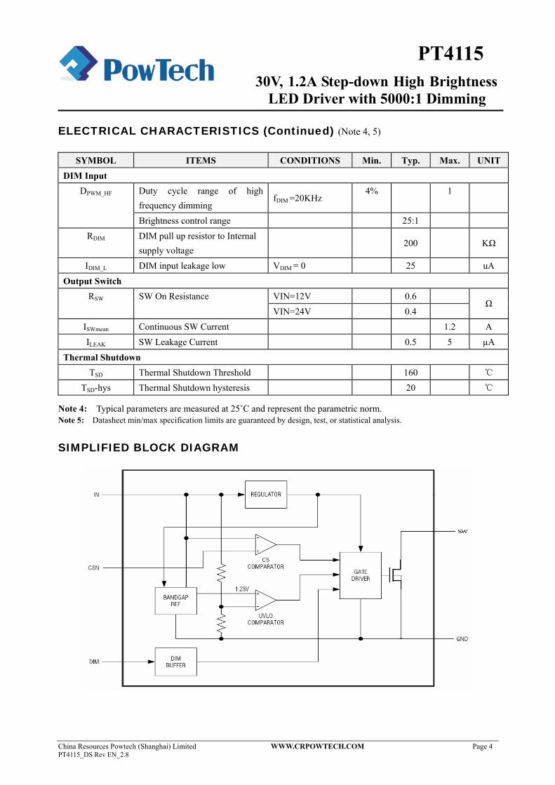
SIMPLIFIED BLOCK DIAGRAM
30V, 1.2A Step-down High Brightness LED Driver with 5000:1 Dimming
China Resources Powtech (Shanghai) Limited WWW.CRPOWTECH.COM Page 5 PT4115_DS Rev EN_2.8
PT4115
OPERATION DESCRIPTION
The device, in conjunction with the coil (L1) and current sense resistor (RS), forms a self oscillating continuous-mode buck converter.
When input voltage VIN is first applied, the initial current in L1 and RS is zero and there is no output from the current sense circuit. Under this condition, the output of CS comparator is high. This turns on an internal switch and switches the SW pin low, causing current to flow from VIN to ground, via RS, L1 and the LED(s). The current rises at a rate determined by VIN and L1 to produce a voltage ramp (VCSN) across RS. When (VIN-VCSN) > 115mV, the output of CS comparator switches low and the switch turns off. The current flowing on the RS decreases at another rate. When (VIN-VCSN) < 85mV, the switch turns on again and the mean current on the LED is determined by
85 1152( ) / 100 /S SmV R mV R+ = .
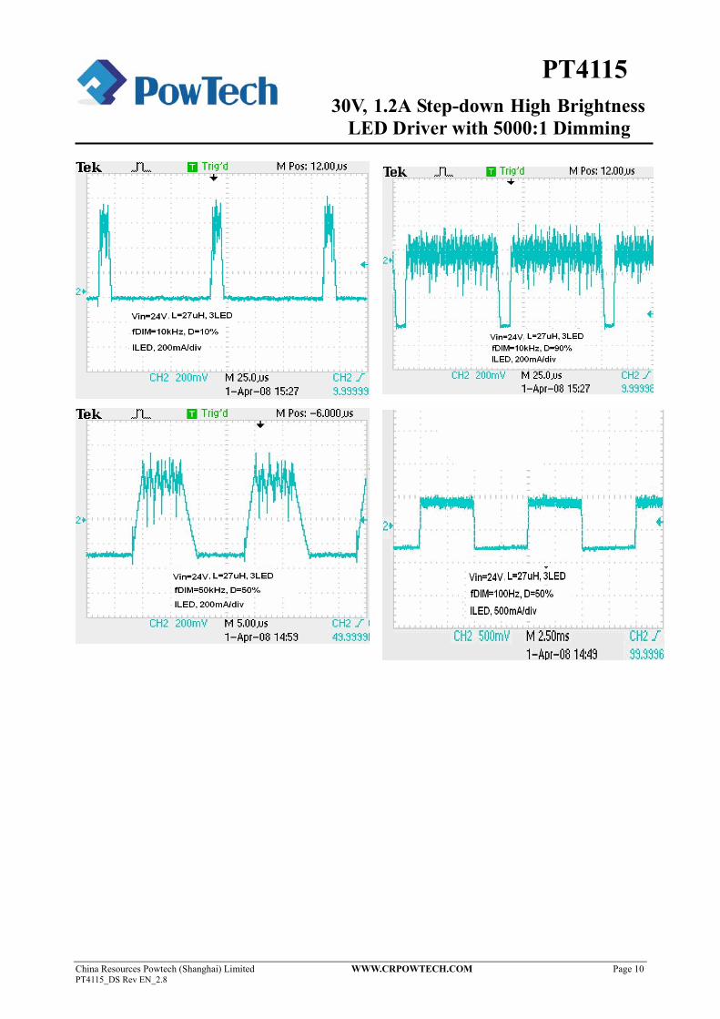
The high-side current-sensing scheme and on-board current-setting circuitry minimize the number of external components while delivering LED current with ±5% accuracy, using a 1% sense resistor. The PT4115 allow dimming with a PWM signal at the DIM input. A logic level below 0.3V at DIM forces PT4115 to turn off the LED and the logic level at DIM must be at least 2.5V to turn on the full LED current. The frequency of PWM dimming ranges from 100Hz to more than 20 kHz.
The DIM pin can be driven by an external DC voltage
(VDIM) to adjust the output current to a value below the nominal average value defined by RS. The DC voltage is valid from 0.5V to 2.5V. When the dc voltage is higher than 2.5V, the output current keeps constant. The LED current also can be adjusted by a resistor connected to the DIM pin. An internal pull-up resistor (typical 200KΩ) is connected to a 5V internal regulator. The voltage of DIM pin is divided by the internal and external resistor.
The DIM pin is pulled up to the internal regulator (5V) by a 200KΩ resistor. It can be floated at normal working. When a voltage applied to DIM falls below the threshold (0.3V nom.), the output switch is turned off. The internal regulator and voltage reference remain powered during shutdown to provide the reference for the shutdown circuit. Quiescent supply current during shutdown is nominally 95uA and switch leakage is below 5uA.
Additionally, to ensure the reliability, the PT4115 is built with a thermal shutdown (TSD) protection and a thermal pad. The TSD protests the IC from over temperature (160). Also the thermal pad enhances power dissipation. As a result, the PT4115 can handle a large amount of current safely.
30V, 1.2A Step-down High Brightness LED Driver with 5000:1 Dimming
China Resources Powtech (Shanghai) Limited WWW.CRPOWTECH.COM Page 6 PT4115_DS Rev EN_2.8
PT4115
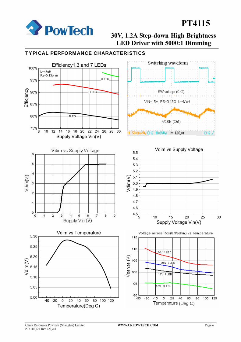
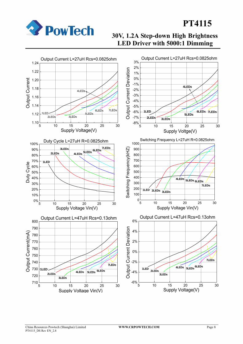
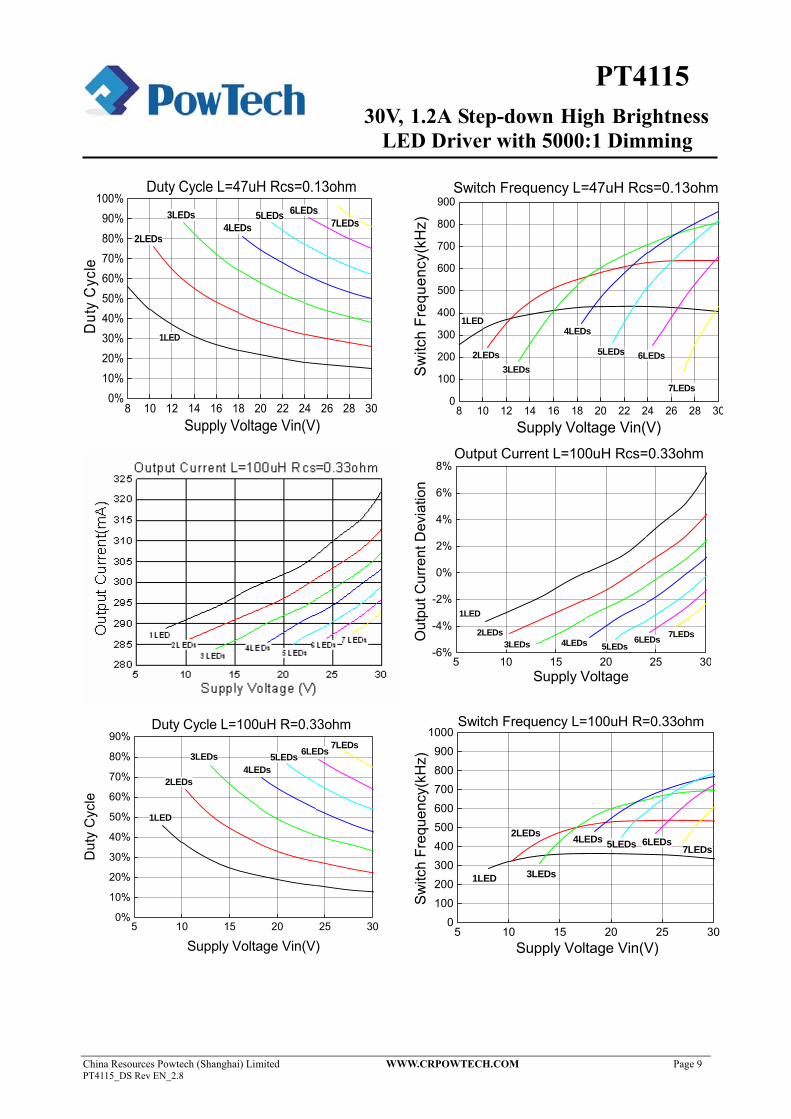
TYPICAL PERFORMANCE CHARACTERISTICS
8 10 12 14 16 18 20 22 24 26 28 3075%
80%
85%
90%
95%
100%
Effic
ienc
y
Supply Voltage Vin(V)
Efficiency1,3 and 7 LEDsL=47uHRs=0.13ohm
1LED
3 LEDs
7LEDs
5 10 15 20 25 304.54.64.74.84.95.05.15.25.35.45.5
Vdi
m(V
)
Supply Voltage Vin(V)
Vdim vs Supply Voltage
-40 -20 0 20 40 60 80 100 1205.00
5.05
5.10
5.15
5.20
5.25
5.30
Vdi
m(V
)
Temperature(Deg C)
Vdim vs Temperature
30V, 1.2A Step-down High Brightness LED Driver with 5000:1 Dimming
China Resources Powtech (Shanghai) Limited WWW.CRPOWTECH.COM Page 7 PT4115_DS Rev EN_2.8
PT4115
5 15 25 350.3
0.4
0.5
0.6
0.7
0.8
0.9
1.0
Rsw
(ohm
)
Supply Voltage Vin(V)
Rsw vs Supply Voltage
0 5 10 15 20 25 300
50
100
150
200
250
Iin (u
A)
Supply Voltage Vin(V)
Supply Current vs Supply Voltage
0 1 2 3 4 50
100
200
300
400
500
600
700
800
R=0.33ohmLED
cur
rent
(mA)
Dim Pin Voltage (V)
LED Current vs Vdim
R=0.13ohm
30V, 1.2A Step-down High Brightness LED Driver with 5000:1 Dimming
China Resources Powtech (Shanghai) Limited WWW.CRPOWTECH.COM Page 8 PT4115_DS Rev EN_2.8
PT4115
5 10 15 20 25 301.10
1.12
1.14
1.16
1.18
1.20
1.22
1.24
7LEDs6LEDs5LEDs
4LEDs
3LEDs2LEDs
Out
put C
urre
nt
Supply Voltage(V)
Output Current L=27uH Rcs=0.0825ohm
1LED
5 10 15 20 25 30-8%-7%-6%-5%-4%-3%-2%-1%0%1%2%3%
7LEDs5LEDs
6LEDs
4LEDs
3LEDsOut
put C
urre
nt D
evia
tion
Supply Voltge(V)
Output Current L=27uH Rcs=0.0825ohm
1LED
2LEDs
5 10 15 20 25 300%
10%20%30%40%50%60%70%80%90%
100%7LEDs
6LEDs5LEDs3LEDs
4LEDs2LEDs
Dut
y C
ycle
Supply Voltage Vin(V)
Duty Cycle L=27uH R=0.0825ohm
1LED
5 10 15 20 25 300
100200300400500600700800900
1000
7LEDs
2LEDs 3LEDs
5LEDs 6LEDs4LEDs
Sw
itchi
ng F
requ
ency
(kH
Z)
Supply Voltage Vin(V)
Switching Frequency L=27uH R=0.0825ohm
1LED
5 10 15 20 25 30710
720
730
740
750
760
770
780
790
800
7LEDs
3LEDs
5LEDs2LEDs6LEDs4LEDsO
utpu
t Cur
rent
(mA
)
Supply Voltage Vin(V)
Output Current L=47uH Rcs=0.13ohm
1LED
5 10 15 20 25 30-6%
-4%
-2%
0%
2%
4%
6%
2LEDs4LEDs 6LEDs
7LEDs
5LEDs
3LEDs
1LED
Out
put C
urre
nt D
evia
tion
Supply Voltage(V)
Output Current L=47uH Rcs=0.13ohm
30V, 1.2A Step-down High Brightness LED Driver with 5000:1 Dimming
China Resources Powtech (Shanghai) Limited WWW.CRPOWTECH.COM Page 9 PT4115_DS Rev EN_2.8
PT4115
8 10 12 14 16 18 20 22 24 26 28 300%
10%20%30%40%50%60%70%80%90%
100%
7LEDs6LEDs5LEDs
4LEDs3LEDs
Dut
y C
ycle
Supply Voltage Vin(V)
Duty Cycle L=47uH Rcs=0.13ohm
1LED
2LEDs
8 10 12 14 16 18 20 22 24 26 28 300
100
200
300
400
500
600
700
800
900
7LEDs
6LEDs5LEDs
4LEDs
3LEDs2LEDs
1LED
Switc
h Fr
eque
ncy(
kHz)
Supply Voltage Vin(V)
Switch Frequency L=47uH Rcs=0.13ohm
5 10 15 20 25 30-6%
-4%
-2%
0%
2%
4%
6%
8%
7LEDs3LEDs 6LEDs
5LEDs4LEDs2LEDs
1LED
Out
put C
urre
nt D
evia
tion
Supply Voltage
Output Current L=100uH Rcs=0.33ohm
5 10 15 20 25 300%
10%
20%
30%
40%
50%
60%
70%
80%
90%7LEDs6LEDs5LEDs
4LEDs3LEDs
Dut
y C
ycle
Supply Voltage Vin(V)
Duty Cycle L=100uH R=0.33ohm
1LED
2LEDs
5 10 15 20 25 30
0100200300400500600700800900
1000
7LEDs6LEDs5LEDs4LEDs
3LEDs
2LEDs
1LED
Sw
itch
Freq
uenc
y(kH
z)
Supply Voltage Vin(V)
Switch Frequency L=100uH R=0.33ohm
30V, 1.2A Step-down High Brightness LED Driver with 5000:1 Dimming
China Resources Powtech (Shanghai) Limited WWW.CRPOWTECH.COM Page 10 PT4115_DS Rev EN_2.8
PT4115
30V, 1.2A Step-down High Brightness LED Driver with 5000:1 Dimming
China Resources Powtech (Shanghai) Limited WWW.CRPOWTECH.COM Page 11 PT4115_DS Rev EN_2.8
PT4115
APPLICATION NOTES
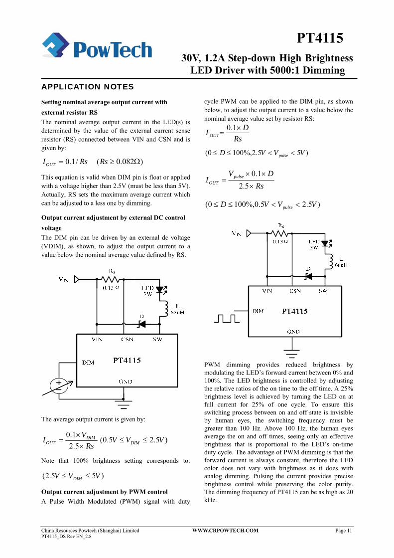
Setting nominal average output current with external resistor RS The nominal average output current in the LED(s) is determined by the value of the external current sense resistor (RS) connected between VIN and CSN and is given by:
RsIOUT /1.0= )082.0( Ω≥Rs
This equation is valid when DIM pin is float or applied with a voltage higher than 2.5V (must be less than 5V). Actually, RS sets the maximum average current which can be adjusted to a less one by dimming.
Output current adjustment by external DC control voltage The DIM pin can be driven by an external dc voltage (VDIM), as shown, to adjust the output current to a value below the nominal average value defined by RS.
The average output current is given by:
RsV
I DIMOUT ×
×=
5.21.0 )5.25.0( VVV DIM ≤≤
Note that 100% brightness setting corresponds to:
)55.2( VVV DIM ≤≤
Output current adjustment by PWM control A Pulse Width Modulated (PWM) signal with duty
cycle PWM can be applied to the DIM pin, as shown below, to adjust the output current to a value below the nominal average value set by resistor RS:
RsDI OUT
×=
1.0
)55.2%,1000( VVVD pulse <<≤≤
RsDV
I pulseOUT ×
××=
5.21.0
)5.25.0%,1000( VVVD pulse <<≤≤
PWM dimming provides reduced brightness by modulating the LED’s forward current between 0% and 100%. The LED brightness is controlled by adjusting the relative ratios of the on time to the off time. A 25% brightness level is achieved by turning the LED on at full current for 25% of one cycle. To ensure this switching process between on and off state is invisible by human eyes, the switching frequency must be greater than 100 Hz. Above 100 Hz, the human eyes average the on and off times, seeing only an effective brightness that is proportional to the LED’s on-time duty cycle. The advantage of PWM dimming is that the forward current is always constant, therefore the LED color does not vary with brightness as it does with analog dimming. Pulsing the current provides precise brightness control while preserving the color purity. The dimming frequency of PT4115 can be as high as 20 kHz.
30V, 1.2A Step-down High Brightness LED Driver with 5000:1 Dimming
China Resources Powtech (Shanghai) Limited WWW.CRPOWTECH.COM Page 12 PT4115_DS Rev EN_2.8
PT4115
Shutdown mode Taking the DIM pin to a voltage below 0.3V will turn off the output and the supply current will fall to a low standby level of 95μA nominal.
Soft-start An external capacitor from the DIM pin to ground will provide additional soft-start delay, by increasing the time taken for the voltage on this pin to rise to the turn-on threshold and by slowing down the rate of rise of the control voltage at the input of the comparator. Adding capacitance increases this delay by approximately 0.8ms/nF.
Inherent open-circuit LED protection If the connection to the LED(s) is open-circuited, the coil is isolated from the SW pin of the chip, so the device and LED will not be damaged.
Capacitor selection A low ESR capacitor should be used for input decoupling, as the ESR of this capacitor appears in series with the supply source impedance and lowers overall efficiency. This capacitor has to supply the relatively high peak current to the coil and smooth the current ripple on the input supply. A minimum value of 4.7uF is acceptable if the DC input source is close to the device, but higher values will improve performance at lower input voltages, especially when the source impedance is high. For the rectified AC input, the capacitor should be higher than 100uF and the tantalum capacitor is recommended. The input capacitor should be placed as close as possible to the IC. For maximum stability over temperature and voltage, capacitors with X7R, X5R, or better dielectric are recommended. Capacitors with Y5V dielectric are not suitable for decoupling in this application and should NOT be used. A suitable Murata capacitor would be GRM42-2X7R475K-50. The following web sites are useful when finding alternatives: www.murata.com www.t-yuden.com www.avxcorp.com
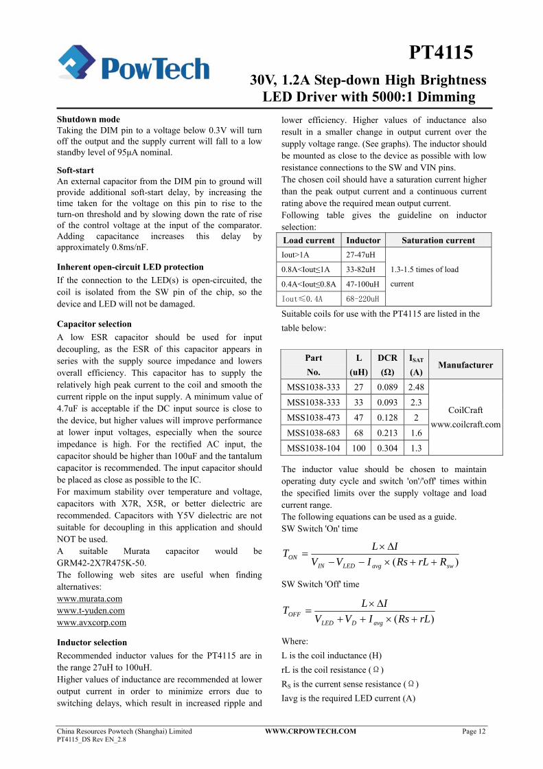
Inductor selection Recommended inductor values for the PT4115 are in the range 27uH to 100uH. Higher values of inductance are recommended at lower output current in order to minimize errors due to switching delays, which result in increased ripple and
lower efficiency. Higher values of inductance also result in a smaller change in output current over the supply voltage range. (See graphs). The inductor should be mounted as close to the device as possible with low resistance connections to the SW and VIN pins. The chosen coil should have a saturation current higher than the peak output current and a continuous current rating above the required mean output current. Following table gives the guideline on inductor selection: Load current Inductor Saturation current Iout>1A 27-47uH 0.8A<Iout≤1A 33-82uH 0.4A<Iout≤0.8A 47-100uH
Iout≤0.4A 68-220uH
1.3-1.5 times of load
current
Suitable coils for use with the PT4115 are listed in the table below:
Part No.
L (uH)
DCR (Ω)
ISAT
(A) Manufacturer
MSS1038-333 27 0.089 2.48
MSS1038-333 33 0.093 2.3
MSS1038-473 47 0.128 2
MSS1038-683 68 0.213 1.6
MSS1038-104 100 0.304 1.3
CoilCraft www.coilcraft.com
The inductor value should be chosen to maintain operating duty cycle and switch 'on'/'off' times within the specified limits over the supply voltage and load current range. The following equations can be used as a guide. SW Switch 'On' time
)( swavgLEDINON RrLRsIVV
ILT++×−−
Δ×=
SW Switch 'Off' time
)( rLRsIVVILT
avgDLEDOFF +×++
Δ×=
Where: L is the coil inductance (H) rL is the coil resistance (Ω) RS is the current sense resistance (Ω) Iavg is the required LED current (A)
30V, 1.2A Step-down High Brightness LED Driver with 5000:1 Dimming
China Resources Powtech (Shanghai) Limited WWW.CRPOWTECH.COM Page 13 PT4115_DS Rev EN_2.8
PT4115
ΔI is the coil peak-peak ripple current (A) Internally set to 0.3 x Iavg VIN is the supply voltage (V) VLED is the total LED forward voltage (V) RSW is the switch resistance (Ω) =0.6Ω nominal VD is the diode forward voltage at the required load current (V)
Diode selection For maximum efficiency and performance, the rectifier (D1) should be a fast low capacitance Schottky diode with low reverse leakage at the maximum operating voltage and temperature. They also provide better efficiency than silicon diodes, due to a combination of lower forward voltage and reduced recovery time. It is important to select parts with a peak current rating above the peak coil current and a continuous current rating higher than the maximum output load current. It is very important to consider the reverse leakage of the diode when operating above 85°C. Excess leakage will increase the power dissipation in the device and if close to the load may create a thermal runaway condition. The higher forward voltage and overshoot due to reverse recovery time in silicon diodes will increase the peak voltage on the SW output. If a silicon diode is used, care should be taken to ensure that the total voltage appearing on the SW pin including supply ripple, does not exceed the specified maximum value. The following web sites are useful when finding alternatives: www.onsemi.com
Reducing output ripple Peak to peak ripple current in the LED(s) can be reduced, if required, by shunting a capacitor CLED across the LED(s) as shown below:
A value of 1uF will reduce the supply ripple current by a factor three (approx.). Proportionally lower ripple can be achieved with higher capacitor values. Note that the capacitor will not affect operating frequency or efficiency, but it will increase start-up delay and reduce the frequency of dimming, by reducing the rate of rise of LED voltage. By adding this capacitor the current waveform through the LED(s) changes from a triangular ramp to a more sinusoidal version without altering the mean current value.
Operation at low supply voltage The internal regulator disables the drive to the switch until the supply has risen above the startup threshold (VUVLO). Above this threshold, the device will start to operate. However, with the supply voltage below the specified minimum value, the switch duty cycle will be high and the device power dissipation will be at a maximum. Care should be taken to avoid operating the device under such conditions in the application, in order to minimize the risk of exceeding the maximum allowed die temperature. (See next section on thermal considerations). The drive to the switch is turned off when the supply voltage falls below the under-voltage threshold (VUVLO-0.5V). This prevents the switch working with excessive 'on' resistance under conditions where the duty cycle is high.
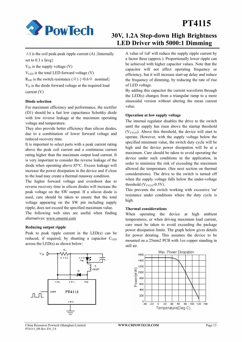
Thermal considerations When operating the device at high ambient temperatures, or when driving maximum load current, care must be taken to avoid exceeding the package power dissipation limits. The graph below gives details for power derating. This assumes the device to be mounted on a 25mm2 PCB with 1oz copper standing in still air.
30V, 1.2A Step-down High Brightness LED Driver with 5000:1 Dimming
China Resources Powtech (Shanghai) Limited WWW.CRPOWTECH.COM Page 14 PT4115_DS Rev EN_2.8
PT4115
Note that the device power dissipation will most often be a maximum at minimum supply voltage. It will also increase if the efficiency of the circuit is low. This may result from the use of unsuitable coils, or excessive parasitic output capacitance on the switch output. When the application is limited by the internal power dissipation of the device, the ESOP8 package is recommended because of its enhanced power dissipation ability.
Thermal compensation of output current High luminance LEDs often need to be supplied with a temperature compensated current in order to maintain stable and reliable operation at all drive levels. The LEDs are usually mounted remotely from the device so,for this reason, the temperature coefficients of the internal circuits for the PT4115 have been optimized to minimize the change in output current when no compensation is employed. If output current compensation is required, it is possible to use an external temperature sensing network - normally using Negative Temperature Coefficient (NTC) thermistors and/or diodes, mounted very close to the LED(s). The output of the sensing network can be used to drive the DIM pin in order to reduce output current with increasing temperature.
Thermal shutdown protection To ensure the reliability, the PT4115 is built with a thermal shutdown (TSD) protection function. The TSD
protests the IC from over temperature (160). When the chip temperature decreases (140), the IC recovers again.
Layout considerations Careful PCB layout is critical to achieve low switching losses and stable operation. Use a multilayer board whenever possible for better noise immunity. Minimize ground noise by connecting high-current ground returns, the input bypass-capacitor ground lead, and the output-filter ground lead to a single point (star ground configuration).
SW pin The SW pin of the device is a fast switching node, so PCB tracks should be kept as short as possible. To minimize ground 'bounce', the ground pin of the device should be soldered directly to the ground plane.
Coil and decoupling capacitors and current sense resistor It is particularly important to mount the coil and the input decoupling capacitor as close to the device pins as possible to minimize parasitic resistance and inductance, which will degrade efficiency. It is also important to minimize any track resistance in series with current sense resistor RS. It’s best to connect VIN directly to one end of RS and CSN directly to the opposite end of RS with no other currents flowing in these tracks. It is important that the cathode current of the Schottky diode does not flow in a track between RS and VIN as this may give an apparent higher measure of current than is actual because of track resistance.
30V, 1.2A Step-down High Brightness LED Driver with 5000:1 Dimming
China Resources Powtech (Shanghai) Limited WWW.CRPOWTECH.COM Page 15 PT4115_DS Rev EN_2.8
PT4115
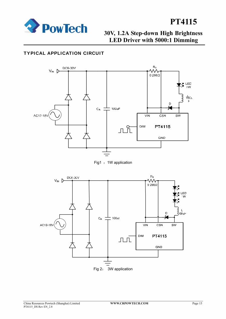
TYPICAL APPLICATION CIRCUIT
Fig1 :1W application
Fig 2: 3W application
30V, 1.2A Step-down High Brightness LED Driver with 5000:1 Dimming
China Resources Powtech (Shanghai) Limited WWW.CRPOWTECH.COM Page 16 PT4115_DS Rev EN_2.8
PT4115
TYPICAL APPLICATION CIRCUIT (Continued)
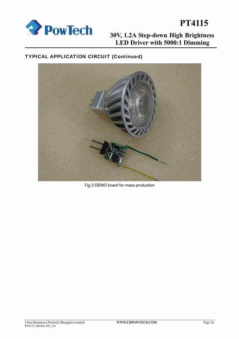
Fig 3 DEMO board for mass production
30V, 1.2A Step-down High Brightness LED Driver with 5000:1 Dimming
China Resources Powtech (Shanghai) Limited WWW.CRPOWTECH.COM Page 17 PT4115_DS Rev EN_2.8
PT4115
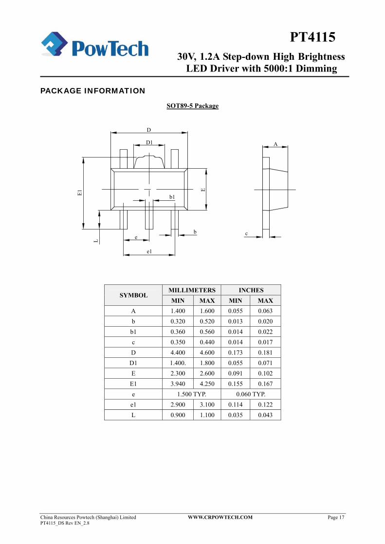
PACKAGE INFORMATION
SOT89-5 Package
MILLIMETERS INCHES
SYMBOL MIN MAX MIN MAX
A 1.400 1.600 0.055 0.063 b 0.320 0.520 0.013 0.020
b1 0.360 0.560 0.014 0.022 c 0.350 0.440 0.014 0.017 D 4.400 4.600 0.173 0.181
D1 1.400. 1.800 0.055 0.071 E 2.300 2.600 0.091 0.102
E1 3.940 4.250 0.155 0.167 e 1.500 TYP. 0.060 TYP.
e1 2.900 3.100 0.114 0.122 L 0.900 1.100 0.035 0.043
D
D1
b1
be
e1
L
E1
E
A
c
30V, 1.2A Step-down High Brightness LED Driver with 5000:1 Dimming
China Resources Powtech (Shanghai) Limited WWW.CRPOWTECH.COM Page 18 PT4115_DS Rev EN_2.8
PT4115
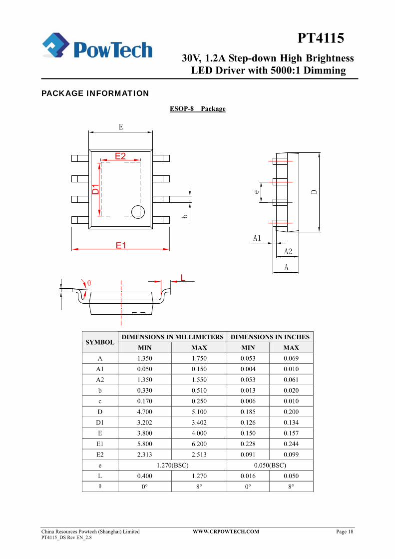
PACKAGE INFORMATION
ESOP-8 Package
DIMENSIONS IN MILLIMETERS DIMENSIONS IN INCHES SYMBOL
MIN MAX MIN MAX A 1.350 1.750 0.053 0.069
A1 0.050 0.150 0.004 0.010 A2 1.350 1.550 0.053 0.061 b 0.330 0.510 0.013 0.020 c 0.170 0.250 0.006 0.010 D 4.700 5.100 0.185 0.200
D1 3.202 3.402 0.126 0.134 E 3.800 4.000 0.150 0.157
E1 5.800 6.200 0.228 0.244 E2 2.313 2.513 0.091 0.099 e 1.270(BSC) 0.050(BSC) L 0.400 1.270 0.016 0.050 θ 0° 8° 0° 8°