Embed Size (px)
Citation preview
4Mb: 3.0V Core Async/Page PSRAM Memory 256K x 16Features
3.0V Core Async/Page PSRAM Memory MT45V256KW16PEGA
Features• Asynchronous and page mode interface • Random access time: 55ns and 70ns• VCC, VCCQ voltages
– 2.7–3.6V VCC
– 2.7–3.6V VCCQ• Page mode read access
– 16-word page size– Interpage read access: 55ns and 70ns– Intrapage read access: 15ns and 20ns
• Low power consumption– Asynchronous READ: <30mA– Intrapage READ: <18mA– Standby: <140µA– Deep power-down (DPD): <45µA (TYP at 25°C)
• Low-power features– Partial-array refresh (PAR)– DPD mode
Options Designator• Configuration
– 256K x 16 MT45V256KW16PE• Package
– 48-ball VFBGA (“green”) GA• Access time
– 55ns -55– 70ns -70
• Operating temperature range– Wireless (–30°C to +85°C) WT– Industrial (–40°C to +85°C) IT
Products and specifications discussed herein are
PDF: 09005aef832450a3/Source: 09005aef82f264aa8mb_4mb_ap_3v_psram_p22z__1.fm - Rev. B 4/08 EN 1
Figure 1: 48-Ball VFBGA Ball Assignments
Part Number Example:
MT45V256KW16PEGA-55WT
A
B
C
D
E
F
G
H
1 2 3 4 5 6
Top view(Ball down)
LB#
DQ8
DQ9
VssQ
VccQ
DQ14
DQ15
DNU
OE#
UB#
DQ10
DQ11
DQ12
DQ13
NC
A8
A0
A3
A5
A17
NC
A14
A12
A9
A2
CE#
DQ1
DQ3
DQ4
DQ5
WE#
A11
A1
A4
A6
A7
A16
A15
A13
A10
ZZ#
DQ0
DQ2
Vcc
Vss
DQ6
DQ7
NC
subject to change by Micron without notice.
Micron Technology, Inc., reserves the right to change products or specifications without notice.©2007 Micron Technology, Inc. All rights reserved.
PDF: 09005aef832450a3/Source: 09005aef82f264aa Micron Technology, Inc., reserves the right to change products or specifications without notice.4mb_ap_3v_psram_p22zTOC.fm - Rev. B 4/08 EN 2 ©2007 Micron Technology, Inc. All rights reserved.
4Mb: 3.0V Core Async/Page PSRAM Memory 256K x 16Table of Contents
Table of ContentsFeatures . . . . . . . . . . . . . . . . . . . . . . . . . . . . . . . . . . . . . . . . . . . . . . . . . . . . . . . . . . . . . . . . . . . . . . . . . . . . . . . . . . . . . . . . . . . . . .1
Options . . . . . . . . . . . . . . . . . . . . . . . . . . . . . . . . . . . . . . . . . . . . . . . . . . . . . . . . . . . . . . . . . . . . . . . . . . . . . . . . . . . . . . . . . . . .1Designator . . . . . . . . . . . . . . . . . . . . . . . . . . . . . . . . . . . . . . . . . . . . . . . . . . . . . . . . . . . . . . . . . . . . . . . . . . . . . . . . . . . . . . . . .1
Table of Contents . . . . . . . . . . . . . . . . . . . . . . . . . . . . . . . . . . . . . . . . . . . . . . . . . . . . . . . . . . . . . . . . . . . . . . . . . . . . . . . . . . . . .2List of Figures . . . . . . . . . . . . . . . . . . . . . . . . . . . . . . . . . . . . . . . . . . . . . . . . . . . . . . . . . . . . . . . . . . . . . . . . . . . . . . . . . . . . . . . . .3List of Tables. . . . . . . . . . . . . . . . . . . . . . . . . . . . . . . . . . . . . . . . . . . . . . . . . . . . . . . . . . . . . . . . . . . . . . . . . . . . . . . . . . . . . . . . . .4General Description . . . . . . . . . . . . . . . . . . . . . . . . . . . . . . . . . . . . . . . . . . . . . . . . . . . . . . . . . . . . . . . . . . . . . . . . . . . . . . . . . . .5Functional Block Diagram. . . . . . . . . . . . . . . . . . . . . . . . . . . . . . . . . . . . . . . . . . . . . . . . . . . . . . . . . . . . . . . . . . . . . . . . . . . . . .5Ball Descriptions . . . . . . . . . . . . . . . . . . . . . . . . . . . . . . . . . . . . . . . . . . . . . . . . . . . . . . . . . . . . . . . . . . . . . . . . . . . . . . . . . . . . . .6Bus Operations . . . . . . . . . . . . . . . . . . . . . . . . . . . . . . . . . . . . . . . . . . . . . . . . . . . . . . . . . . . . . . . . . . . . . . . . . . . . . . . . . . . . . . .7Part Numbering Information . . . . . . . . . . . . . . . . . . . . . . . . . . . . . . . . . . . . . . . . . . . . . . . . . . . . . . . . . . . . . . . . . . . . . . . . . . .8
Valid Part Number Combinations . . . . . . . . . . . . . . . . . . . . . . . . . . . . . . . . . . . . . . . . . . . . . . . . . . . . . . . . . . . . . . . . . . . .8Device Marking. . . . . . . . . . . . . . . . . . . . . . . . . . . . . . . . . . . . . . . . . . . . . . . . . . . . . . . . . . . . . . . . . . . . . . . . . . . . . . . . . . . . .8
Functional Description . . . . . . . . . . . . . . . . . . . . . . . . . . . . . . . . . . . . . . . . . . . . . . . . . . . . . . . . . . . . . . . . . . . . . . . . . . . . . . . .9Power-Up Initialization . . . . . . . . . . . . . . . . . . . . . . . . . . . . . . . . . . . . . . . . . . . . . . . . . . . . . . . . . . . . . . . . . . . . . . . . . . . . . . . .9Bus Operating Modes . . . . . . . . . . . . . . . . . . . . . . . . . . . . . . . . . . . . . . . . . . . . . . . . . . . . . . . . . . . . . . . . . . . . . . . . . . . . . . . . . .9
Asynchronous Mode . . . . . . . . . . . . . . . . . . . . . . . . . . . . . . . . . . . . . . . . . . . . . . . . . . . . . . . . . . . . . . . . . . . . . . . . . . . . . . . .9Page Mode READ Operation . . . . . . . . . . . . . . . . . . . . . . . . . . . . . . . . . . . . . . . . . . . . . . . . . . . . . . . . . . . . . . . . . . . . . . . .11LB#/UB# Operation . . . . . . . . . . . . . . . . . . . . . . . . . . . . . . . . . . . . . . . . . . . . . . . . . . . . . . . . . . . . . . . . . . . . . . . . . . . . . . . .11
Low-Power Operation . . . . . . . . . . . . . . . . . . . . . . . . . . . . . . . . . . . . . . . . . . . . . . . . . . . . . . . . . . . . . . . . . . . . . . . . . . . . . . . .12Standby Mode Operation . . . . . . . . . . . . . . . . . . . . . . . . . . . . . . . . . . . . . . . . . . . . . . . . . . . . . . . . . . . . . . . . . . . . . . . . . . .12Partial-Array Refresh . . . . . . . . . . . . . . . . . . . . . . . . . . . . . . . . . . . . . . . . . . . . . . . . . . . . . . . . . . . . . . . . . . . . . . . . . . . . . . .12Deep Power-Down Operation . . . . . . . . . . . . . . . . . . . . . . . . . . . . . . . . . . . . . . . . . . . . . . . . . . . . . . . . . . . . . . . . . . . . . . .13
Configuration Register Operation . . . . . . . . . . . . . . . . . . . . . . . . . . . . . . . . . . . . . . . . . . . . . . . . . . . . . . . . . . . . . . . . . . . . . .14Access Using ZZ# . . . . . . . . . . . . . . . . . . . . . . . . . . . . . . . . . . . . . . . . . . . . . . . . . . . . . . . . . . . . . . . . . . . . . . . . . . . . . . . . . .14Software Access to the Configuration Register . . . . . . . . . . . . . . . . . . . . . . . . . . . . . . . . . . . . . . . . . . . . . . . . . . . . . . . .15
Electrical Characteristics . . . . . . . . . . . . . . . . . . . . . . . . . . . . . . . . . . . . . . . . . . . . . . . . . . . . . . . . . . . . . . . . . . . . . . . . . . . . . .17Maximum and Typical Standby Currents . . . . . . . . . . . . . . . . . . . . . . . . . . . . . . . . . . . . . . . . . . . . . . . . . . . . . . . . . . . . .18
Timing Diagrams. . . . . . . . . . . . . . . . . . . . . . . . . . . . . . . . . . . . . . . . . . . . . . . . . . . . . . . . . . . . . . . . . . . . . . . . . . . . . . . . . . . . .21Package Dimensions . . . . . . . . . . . . . . . . . . . . . . . . . . . . . . . . . . . . . . . . . . . . . . . . . . . . . . . . . . . . . . . . . . . . . . . . . . . . . . . . .25Revision History. . . . . . . . . . . . . . . . . . . . . . . . . . . . . . . . . . . . . . . . . . . . . . . . . . . . . . . . . . . . . . . . . . . . . . . . . . . . . . . . . . . . . .26
PDF: 09005aef832450a3/Source: 09005aef82f264aa Micron Technology, Inc., reserves the right to change products or specifications without notice.4mb_ap_3v_psram_p22zLOF.fm - Rev. B 4/08 EN 3 ©2007 Micron Technology, Inc. All rights reserved.
4Mb: 3.0V Core Async/Page PSRAM Memory 256K x 16List of Figures
List of FiguresFigure 1: 48-Ball VFBGA Ball Assignments. . . . . . . . . . . . . . . . . . . . . . . . . . . . . . . . . . . . . . . . . . . . . . . . . . . . . . . . . . . .1Figure 2: Functional Block Diagram 256K x 16 . . . . . . . . . . . . . . . . . . . . . . . . . . . . . . . . . . . . . . . . . . . . . . . . . . . . . . . .5Figure 3: Part Number Chart . . . . . . . . . . . . . . . . . . . . . . . . . . . . . . . . . . . . . . . . . . . . . . . . . . . . . . . . . . . . . . . . . . . . . . . .8Figure 4: Power-Up Initialization Timing. . . . . . . . . . . . . . . . . . . . . . . . . . . . . . . . . . . . . . . . . . . . . . . . . . . . . . . . . . . . .9Figure 5: READ Operation . . . . . . . . . . . . . . . . . . . . . . . . . . . . . . . . . . . . . . . . . . . . . . . . . . . . . . . . . . . . . . . . . . . . . . . . .10Figure 6: WRITE Operation . . . . . . . . . . . . . . . . . . . . . . . . . . . . . . . . . . . . . . . . . . . . . . . . . . . . . . . . . . . . . . . . . . . . . . . .10Figure 7: Page Mode READ Operation (ADV = LOW). . . . . . . . . . . . . . . . . . . . . . . . . . . . . . . . . . . . . . . . . . . . . . . . . .11Figure 8: Software Access PAR Functionality. . . . . . . . . . . . . . . . . . . . . . . . . . . . . . . . . . . . . . . . . . . . . . . . . . . . . . . . .13Figure 9: Configuration Register Bit Mapping. . . . . . . . . . . . . . . . . . . . . . . . . . . . . . . . . . . . . . . . . . . . . . . . . . . . . . . .14Figure 10: Load Configuration Register Operation Using ZZ#. . . . . . . . . . . . . . . . . . . . . . . . . . . . . . . . . . . . . . . . . . .14Figure 11: Load Configuration Register . . . . . . . . . . . . . . . . . . . . . . . . . . . . . . . . . . . . . . . . . . . . . . . . . . . . . . . . . . . . . .15Figure 12: Read Configuration Register . . . . . . . . . . . . . . . . . . . . . . . . . . . . . . . . . . . . . . . . . . . . . . . . . . . . . . . . . . . . . .16Figure 13: Typical Refresh Current vs. Temperature . . . . . . . . . . . . . . . . . . . . . . . . . . . . . . . . . . . . . . . . . . . . . . . . . . .18Figure 14: AC Input/Output Reference Waveform . . . . . . . . . . . . . . . . . . . . . . . . . . . . . . . . . . . . . . . . . . . . . . . . . . . . .19Figure 15: Output Load Circuit . . . . . . . . . . . . . . . . . . . . . . . . . . . . . . . . . . . . . . . . . . . . . . . . . . . . . . . . . . . . . . . . . . . . . .19Figure 16: Power-Up Initialization Period . . . . . . . . . . . . . . . . . . . . . . . . . . . . . . . . . . . . . . . . . . . . . . . . . . . . . . . . . . . .21Figure 17: Load Configuration Register . . . . . . . . . . . . . . . . . . . . . . . . . . . . . . . . . . . . . . . . . . . . . . . . . . . . . . . . . . . . . .21Figure 18: Deep Power-Down Entry and Exit . . . . . . . . . . . . . . . . . . . . . . . . . . . . . . . . . . . . . . . . . . . . . . . . . . . . . . . . .21Figure 19: Single READ Operation (WE# = VIH). . . . . . . . . . . . . . . . . . . . . . . . . . . . . . . . . . . . . . . . . . . . . . . . . . . . . . . .22Figure 20: Page Mode READ Operation (WE# = VIH) . . . . . . . . . . . . . . . . . . . . . . . . . . . . . . . . . . . . . . . . . . . . . . . . . . .22Figure 21: WRITE Cycle (WE# Control) . . . . . . . . . . . . . . . . . . . . . . . . . . . . . . . . . . . . . . . . . . . . . . . . . . . . . . . . . . . . . . .23Figure 22: WRITE Cycle (CE# Control) . . . . . . . . . . . . . . . . . . . . . . . . . . . . . . . . . . . . . . . . . . . . . . . . . . . . . . . . . . . . . . .23Figure 23: WRITE Cycle (LB#/UB# Control). . . . . . . . . . . . . . . . . . . . . . . . . . . . . . . . . . . . . . . . . . . . . . . . . . . . . . . . . . .24Figure 24: 48-Ball VFBGA . . . . . . . . . . . . . . . . . . . . . . . . . . . . . . . . . . . . . . . . . . . . . . . . . . . . . . . . . . . . . . . . . . . . . . . . . . .25
PDF: 09005aef832450a3/Source: 09005aef82f264aa Micron Technology, Inc., reserves the right to change products or specifications without notice.4mb_ap_3v_psram_p22zLOT.fm - Rev. B 4/08 EN 4 ©2007 Micron Technology, Inc. All rights reserved.
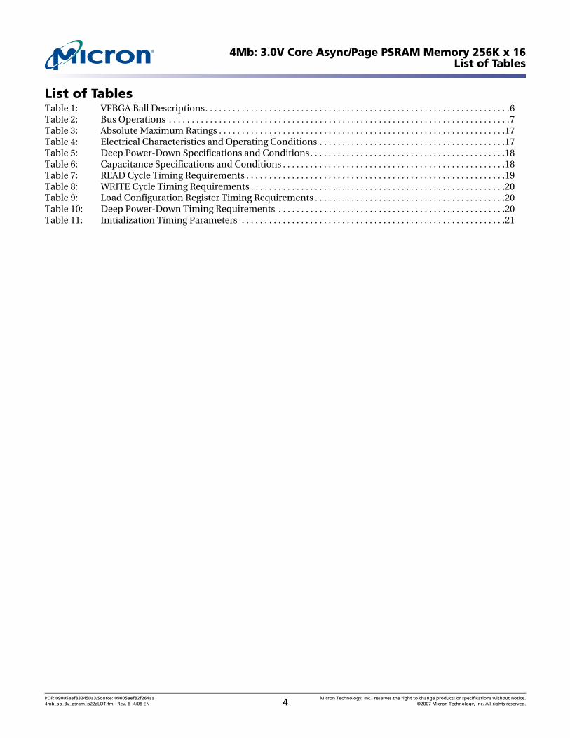
4Mb: 3.0V Core Async/Page PSRAM Memory 256K x 16List of Tables
List of TablesTable 1: VFBGA Ball Descriptions. . . . . . . . . . . . . . . . . . . . . . . . . . . . . . . . . . . . . . . . . . . . . . . . . . . . . . . . . . . . . . . . . . .6Table 2: Bus Operations . . . . . . . . . . . . . . . . . . . . . . . . . . . . . . . . . . . . . . . . . . . . . . . . . . . . . . . . . . . . . . . . . . . . . . . . . . .7Table 3: Absolute Maximum Ratings . . . . . . . . . . . . . . . . . . . . . . . . . . . . . . . . . . . . . . . . . . . . . . . . . . . . . . . . . . . . . . .17Table 4: Electrical Characteristics and Operating Conditions . . . . . . . . . . . . . . . . . . . . . . . . . . . . . . . . . . . . . . . . .17Table 5: Deep Power-Down Specifications and Conditions. . . . . . . . . . . . . . . . . . . . . . . . . . . . . . . . . . . . . . . . . . .18Table 6: Capacitance Specifications and Conditions . . . . . . . . . . . . . . . . . . . . . . . . . . . . . . . . . . . . . . . . . . . . . . . . .18Table 7: READ Cycle Timing Requirements . . . . . . . . . . . . . . . . . . . . . . . . . . . . . . . . . . . . . . . . . . . . . . . . . . . . . . . . .19Table 8: WRITE Cycle Timing Requirements . . . . . . . . . . . . . . . . . . . . . . . . . . . . . . . . . . . . . . . . . . . . . . . . . . . . . . . .20Table 9: Load Configuration Register Timing Requirements . . . . . . . . . . . . . . . . . . . . . . . . . . . . . . . . . . . . . . . . . .20Table 10: Deep Power-Down Timing Requirements . . . . . . . . . . . . . . . . . . . . . . . . . . . . . . . . . . . . . . . . . . . . . . . . . .20Table 11: Initialization Timing Parameters . . . . . . . . . . . . . . . . . . . . . . . . . . . . . . . . . . . . . . . . . . . . . . . . . . . . . . . . . .21
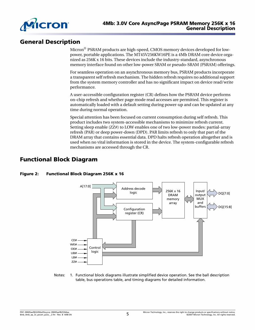
4Mb: 3.0V Core Async/Page PSRAM Memory 256K x 16General Description
General DescriptionMicron® PSRAM products are high-speed, CMOS memory devices developed for low-power, portable applications. The MT45V256KW16PE is a 4Mb DRAM core device orga-nized as 256K x 16 bits. These devices include the industry-standard, asynchronous memory interface found on other low-power SRAM or pseudo-SRAM (PSRAM) offerings.
For seamless operation on an asynchronous memory bus, PSRAM products incorporate a transparent self refresh mechanism. The hidden refresh requires no additional support from the system memory controller and has no significant impact on device read/write performance.
A user-accessible configuration register (CR) defines how the PSRAM device performs on-chip refresh and whether page mode read accesses are permitted. This register is automatically loaded with a default setting during power-up and can be updated at any time during normal operation.
Special attention has been focused on current consumption during self refresh. This product includes two system-accessible mechanisms to minimize refresh current. Setting sleep enable (ZZ#) to LOW enables one of two low-power modes: partial-array refresh (PAR) or deep power-down (DPD). PAR limits refresh to only that part of the DRAM array that contains essential data. DPD halts refresh operation altogether and is used when no vital information is stored in the device. The system-configurable refresh mechanisms are accessed through the CR.
Functional Block Diagram
Figure 2: Functional Block Diagram 256K x 16
Notes: 1. Functional block diagrams illustrate simplified device operation. See the ball description table, bus operations table, and timing diagrams for detailed information.
A[17:0]
DQ[7:0]
DQ[15:8]
LB #
UB #
CE #
WE #
OE #
ZZ #
Controllogic
Input/outputMUXand
buffers
256K x 16DRAM
memoryarray
Configurationregister (CR)
Address decodelogic
PDF: 09005aef832450a3/Source: 09005aef82f264aa Micron Technology, Inc., reserves the right to change products or specifications without notice.8mb_4mb_ap_3v_psram_p22z__2.fm - Rev. B 4/08 EN 5 ©2007 Micron Technology, Inc. All rights reserved.
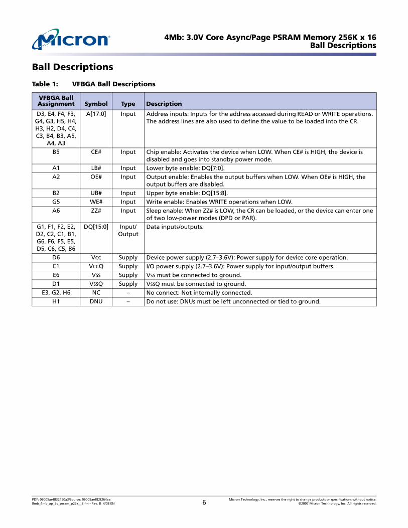
4Mb: 3.0V Core Async/Page PSRAM Memory 256K x 16Ball Descriptions
Ball Descriptions
Table 1: VFBGA Ball Descriptions
VFBGA Ball Assignment Symbol Type Description
D3, E4, F4, F3, G4, G3, H5, H4, H3, H2, D4, C4, C3, B4, B3, A5,
A4, A3
A[17:0] Input Address inputs: Inputs for the address accessed during READ or WRITE operations. The address lines are also used to define the value to be loaded into the CR.
B5 CE# Input Chip enable: Activates the device when LOW. When CE# is HIGH, the device is disabled and goes into standby power mode.
A1 LB# Input Lower byte enable: DQ[7:0].A2 OE# Input Output enable: Enables the output buffers when LOW. When OE# is HIGH, the
output buffers are disabled.B2 UB# Input Upper byte enable: DQ[15:8].G5 WE# Input Write enable: Enables WRITE operations when LOW.A6 ZZ# Input Sleep enable: When ZZ# is LOW, the CR can be loaded, or the device can enter one
of two low-power modes (DPD or PAR).G1, F1, F2, E2, D2, C2, C1, B1, G6, F6, F5, E5, D5, C6, C5, B6
DQ[15:0] Input/Output
Data inputs/outputs.
D6 VCC Supply Device power supply (2.7–3.6V): Power supply for device core operation.E1 VCCQ Supply I/O power supply (2.7–3.6V): Power supply for input/output buffers.E6 VSS Supply VSS must be connected to ground.D1 VSSQ Supply VSSQ must be connected to ground.
E3, G2, H6 NC – No connect: Not internally connected.H1 DNU – Do not use: DNUs must be left unconnected or tied to ground.
PDF: 09005aef832450a3/Source: 09005aef82f264aa Micron Technology, Inc., reserves the right to change products or specifications without notice.8mb_4mb_ap_3v_psram_p22z__2.fm - Rev. B 4/08 EN 6 ©2007 Micron Technology, Inc. All rights reserved.
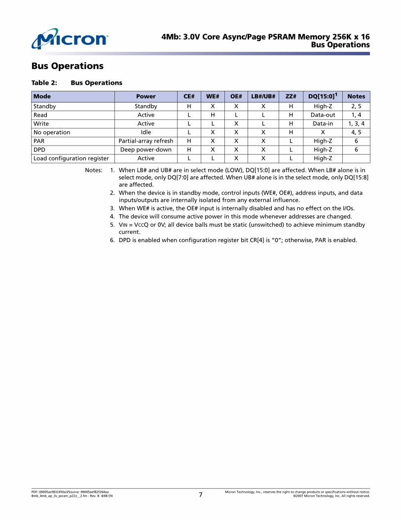
4Mb: 3.0V Core Async/Page PSRAM Memory 256K x 16Bus Operations
Bus Operations
Notes: 1. When LB# and UB# are in select mode (LOW), DQ[15:0] are affected. When LB# alone is in select mode, only DQ[7:0] are affected. When UB# alone is in the select mode, only DQ[15:8] are affected.
2. When the device is in standby mode, control inputs (WE#, OE#), address inputs, and data inputs/outputs are internally isolated from any external influence.
3. When WE# is active, the OE# input is internally disabled and has no effect on the I/Os.4. The device will consume active power in this mode whenever addresses are changed. 5. VIN = VCCQ or 0V; all device balls must be static (unswitched) to achieve minimum standby
current.6. DPD is enabled when configuration register bit CR[4] is “0”; otherwise, PAR is enabled.
Table 2: Bus Operations
Mode Power CE# WE# OE# LB#/UB# ZZ# DQ[15:0]1 Notes
Standby Standby H X X X H High-Z 2, 5
Read Active L H L L H Data-out 1, 4
Write Active L L X L H Data-in 1, 3, 4
No operation Idle L X X X H X 4, 5
PAR Partial-array refresh H X X X L High-Z 6
DPD Deep power-down H X X X L High-Z 6
Load configuration register Active L L X X L High-Z
PDF: 09005aef832450a3/Source: 09005aef82f264aa Micron Technology, Inc., reserves the right to change products or specifications without notice.8mb_4mb_ap_3v_psram_p22z__2.fm - Rev. B 4/08 EN 7 ©2007 Micron Technology, Inc. All rights reserved.
4Mb: 3.0V Core Async/Page PSRAM Memory 256K x 16Part Numbering Information
Part Numbering InformationMicron PSRAM devices are available in several configurations and densities (see Figure 3).
Figure 3: Part Number Chart
Valid Part Number Combinations
After building the part number using the part numbering chart, visit the Micron Web site at www.micron.com/psram to verify that the part number is offered and valid. If the device required is not on this list, contact the factory.
Device Marking
Due to the size of the package, the Micron-standard part number is not printed on the top of the device. Instead, an abbreviated device mark consisting of a five-digit alphanu-meric code is used. The abbreviated device marks are cross-referenced to the Micron part numbers at the FBGA Part Marking Decoder site: www.micron.com/decoder. To view the location of the abbreviated mark on the device, refer to customer service note CSN-11, “Product Mark/Label,” at www.micron.com/csn.
MT 45 V 256K W 16 PE GA -55 WT ES
Micron Technology
Product Family45 = PSRAM memory
Operating Core VoltageV = 2.7V–3.6V
Address LocationsK = Kilobits
Operating VoltageW = 2.7V–3.6V
Bus Configuration16 = x16
READ/WRITE Operation ModePE = Asynchronous/Page
Package CodesGA = VFBGA “Green” (6 x 8 grid, 0.75mm pitch, 6.0mm x 8.0mm x 1.0mm) 48-ball
Production StatusBlank = Production
ES = Engineering sample
MS = Mechanical sample
Operating TemperatureWT = −30°C to +85°C
IT = −40°C to +85°C
Standby Power OptionsBlank = Standard
Access/Cycle Time55 = 55ns
70 = 70ns
PDF: 09005aef832450a3/Source: 09005aef82f264aa Micron Technology, Inc., reserves the right to change products or specifications without notice.8mb_4mb_ap_3v_psram_p22z__2.fm - Rev. B 4/08 EN 8 ©2007 Micron Technology, Inc. All rights reserved.
4Mb: 3.0V Core Async/Page PSRAM Memory 256K x 16Functional Description
Functional DescriptionIn general, MT45V256KW16PE devices are high-density alternatives to SRAM and PSRAM products that are popular in low-power, portable applications.
MT45V256KW16PE devices contain an 4,194,304-bit DRAM core organized as 262,144 addresses by 16 bits. These devices include the industry-standard, asynchronous memory interface found on other low-power SRAM or PSRAM offerings.
Page mode access is also supported as a bandwidth-enhancing extension to the asyn-chronous read protocol.
Power-Up InitializationMicron PSRAM products include an on-chip voltage sensor that is used to launch the power-up initialization process. Initialization will load the CR with its default setting. VCC and VCCQ must be applied simultaneously, and when they reach a stable level above 1.7V, the device will require 150µs to complete its self-initialization process (see Figure 4). During the initialization period, CE# should remain HIGH. When initialization is complete, the device is ready for normal operation.
Figure 4: Power-Up Initialization Timing
Bus Operating ModesThe MT45V256KW16PE PSRAM product incorporates the industry-standard, asynchro-nous interface. This bus interface supports asynchronous READ and WRITE operations as well as page mode READ operation for enhanced bandwidth. The supported interface is defined by the value loaded into the CR.
Asynchronous Mode
Micron PSRAM products power up in the asynchronous operating mode. This mode uses the industry-standard SRAM control interface (CE#, OE#, WE#, and LB#/UB#). READ operations are initiated by bringing CE#, OE#, and LB#/UB# LOW while keeping WE# HIGH (see Figure 5 on page 10). Valid data will be driven out of the I/Os after the specified access time has elapsed. WRITE operations occur when CE#, WE#, and LB#/UB# are driven LOW (see Figure 6 on page 10). During WRITE operations, the level of OE# is a “Don’t Care”; WE# overrides OE#. The data to be written is latched on the rising edge of CE#, WE#, or LB#/UB#, whichever occurs first. WE# LOW time must be limited to tCEM.
Device ready fornormal operation
Vcc, VccQ = 2.7VtPU
Vcc (MIN)
PDF: 09005aef832450a3/Source: 09005aef82f264aa Micron Technology, Inc., reserves the right to change products or specifications without notice.8mb_4mb_ap_3v_psram_p22z__2.fm - Rev. B 4/08 EN 9 ©2007 Micron Technology, Inc. All rights reserved.
4Mb: 3.0V Core Async/Page PSRAM Memory 256K x 16Bus Operating Modes
Figure 5: READ Operation
Figure 6: WRITE Operation
Valid address
Data
CE#
Don’t Care
OE#
WE#
LB#/UB#
tRC = READ cycle time
Address
Valid data
Valid address
Data
CE#
Don’t Care
OE#
WE#
LB#/UB#
tWC = WRITE cycle time
<tCEM
Address
Valid data
PDF: 09005aef832450a3/Source: 09005aef82f264aa Micron Technology, Inc., reserves the right to change products or specifications without notice.8mb_4mb_ap_3v_psram_p22z__2.fm - Rev. B 4/08 EN 10 ©2007 Micron Technology, Inc. All rights reserved.
4Mb: 3.0V Core Async/Page PSRAM Memory 256K x 16Bus Operating Modes
Page Mode READ Operation
Page mode is a performance-enhancing extension to the legacy asynchronous READ operation. In page-mode-capable products, an initial asynchronous read access is performed, then adjacent addresses can be read quickly by simply changing the low-order address. Addresses A[3:0] are used to determine the members of the 16-address PSRAM page. Any change in addresses A[4] or higher will initiate a new tAA access (see Figure 7).
Page mode takes advantage of the fact that adjacent addresses can be read faster than random addresses. WRITE operations do not include comparable page mode function-ality.
The CE# LOW time is limited by refresh considerations. CE# must not stay LOW longer than tCEM.
Figure 7: Page Mode READ Operation (ADV = LOW)
LB#/UB# Operation
The lower byte (LB#) and upper byte (UB#) enable signals accommodate byte-wide data transfers. During READ operations, enabled bytes are driven onto the DQ. The DQ signals associated with a disabled byte are put into a High-Z state during a READ opera-tion. During WRITE operations, disabled bytes are not transferred to the memory array, and the internal value remains unchanged. During a WRITE cycle, the data to be written is latched on the rising edge of CE#, WE#, LB#, or UB#, whichever occurs first.
When both the LB# and UB# are disabled (HIGH) during an operation, the device prevents the data bus from receiving or transmitting data. Although the device may appear to be deselected, it remains in active mode as long as CE# remains LOW.
Data
CE# CE#
OE#
WE#
LB#/UB#
Address Address[0]
D[1] D[2] D[3]
tAA tAPA tAPA tAPA
D[0]
< tCEM
Address [2]
Don't Care
Address [1]
Address [3]
PDF: 09005aef832450a3/Source: 09005aef82f264aa Micron Technology, Inc., reserves the right to change products or specifications without notice.8mb_4mb_ap_3v_psram_p22z__2.fm - Rev. B 4/08 EN 11 ©2007 Micron Technology, Inc. All rights reserved.
4Mb: 3.0V Core Async/Page PSRAM Memory 256K x 16Low-Power Operation
Low-Power Operation
Standby Mode Operation
During standby, the device current consumption is reduced to the level necessary to perform the DRAM REFRESH operation on the full array. Standby operation occurs when CE# and ZZ# are HIGH.
The device enters a reduced-power state upon completion of READ and WRITE opera-tions when the address and control inputs remain static for an extended period of time. This mode continues until a change occurs to the address or control inputs.
Partial-Array Refresh
Partial-array refresh (PAR) restricts REFRESH operation to a portion of the total memory array. This feature enables the system to reduce refresh current by only refreshing that part of the memory array that is absolutely necessary. The refresh options are “full array” and “none of the array.” Data stored in addresses not receiving refresh will become corrupted. READ and WRITE operations are ignored during PAR operation.
The device only enters PAR mode if the sleep bit in the CR has been set HIGH (CR[4] = 1). PAR can be initiated by taking the ZZ# ball to the LOW state for longer than 10µs. Returning ZZ# to HIGH will cause an exit from PAR, and the entire array will be immedi-ately available for READ and WRITE operations.
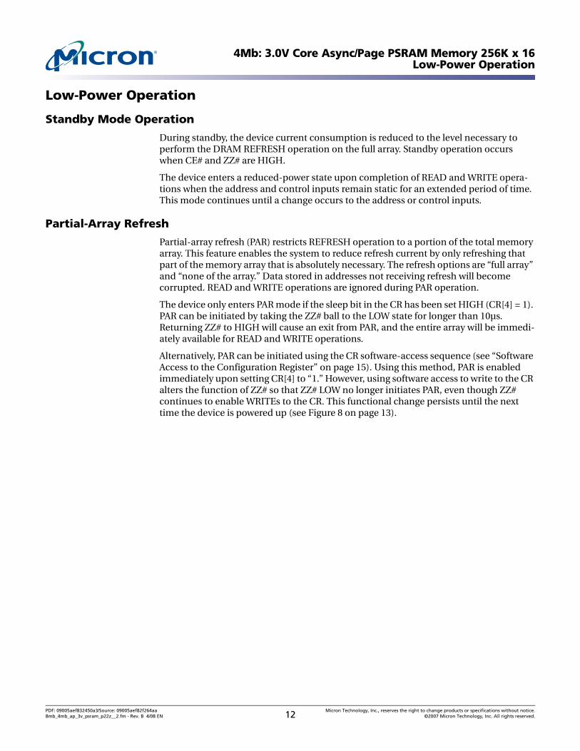
Alternatively, PAR can be initiated using the CR software-access sequence (see “Software Access to the Configuration Register” on page 15). Using this method, PAR is enabled immediately upon setting CR[4] to “1.” However, using software access to write to the CR alters the function of ZZ# so that ZZ# LOW no longer initiates PAR, even though ZZ# continues to enable WRITEs to the CR. This functional change persists until the next time the device is powered up (see Figure 8 on page 13).
PDF: 09005aef832450a3/Source: 09005aef82f264aa Micron Technology, Inc., reserves the right to change products or specifications without notice.8mb_4mb_ap_3v_psram_p22z__2.fm - Rev. B 4/08 EN 12 ©2007 Micron Technology, Inc. All rights reserved.
4Mb: 3.0V Core Async/Page PSRAM Memory 256K x 16Low-Power Operation
Figure 8: Software Access PAR Functionality
Deep Power-Down Operation
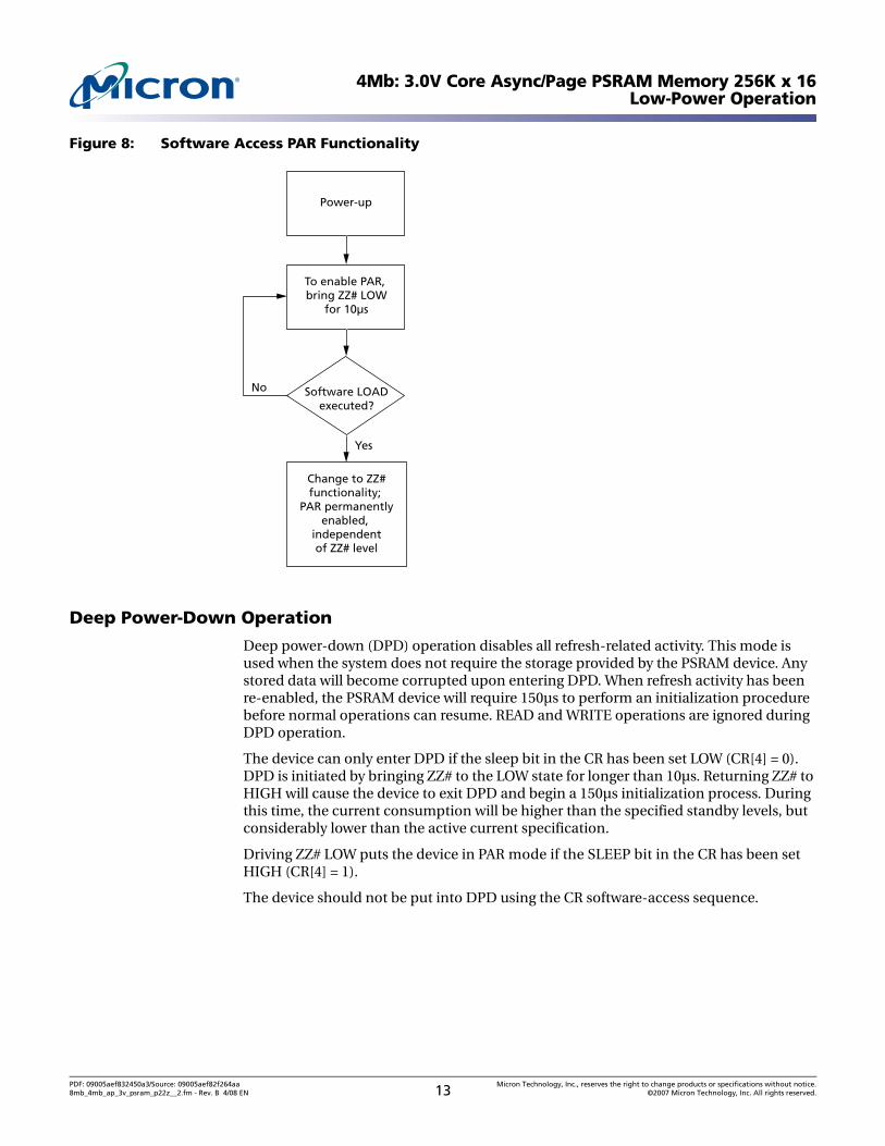
Deep power-down (DPD) operation disables all refresh-related activity. This mode is used when the system does not require the storage provided by the PSRAM device. Any stored data will become corrupted upon entering DPD. When refresh activity has been re-enabled, the PSRAM device will require 150µs to perform an initialization procedure before normal operations can resume. READ and WRITE operations are ignored during DPD operation.
The device can only enter DPD if the sleep bit in the CR has been set LOW (CR[4] = 0). DPD is initiated by bringing ZZ# to the LOW state for longer than 10µs. Returning ZZ# to HIGH will cause the device to exit DPD and begin a 150µs initialization process. During this time, the current consumption will be higher than the specified standby levels, but considerably lower than the active current specification.
Driving ZZ# LOW puts the device in PAR mode if the SLEEP bit in the CR has been set HIGH (CR[4] = 1).
The device should not be put into DPD using the CR software-access sequence.
To enable PAR, bring ZZ# LOW
for 10µs
Power-up
No Software LOADexecuted?
Yes
Change to ZZ#functionality;
PAR permanentlyenabled,
independentof ZZ# level
PDF: 09005aef832450a3/Source: 09005aef82f264aa Micron Technology, Inc., reserves the right to change products or specifications without notice.8mb_4mb_ap_3v_psram_p22z__2.fm - Rev. B 4/08 EN 13 ©2007 Micron Technology, Inc. All rights reserved.
4Mb: 3.0V Core Async/Page PSRAM Memory 256K x 16Configuration Register Operation
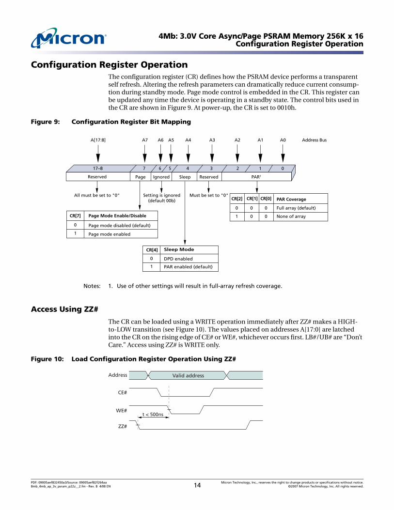
Configuration Register OperationThe configuration register (CR) defines how the PSRAM device performs a transparent self refresh. Altering the refresh parameters can dramatically reduce current consump-tion during standby mode. Page mode control is embedded in the CR. This register can be updated any time the device is operating in a standby state. The control bits used in the CR are shown in Figure 9. At power-up, the CR is set to 0010h.
Figure 9: Configuration Register Bit Mapping
Notes: 1. Use of other settings will result in full-array refresh coverage.
Access Using ZZ#
The CR can be loaded using a WRITE operation immediately after ZZ# makes a HIGH-to-LOW transition (see Figure 10). The values placed on addresses A[17:0] are latched into the CR on the rising edge of CE# or WE#, whichever occurs first. LB#/UB# are “Don’t Care.” Access using ZZ# is WRITE only.
Figure 10: Load Configuration Register Operation Using ZZ#
PAR1
A4 A3 A2 A1 A0 Address Bus
4 123 0
Reserved
6 5
A5
0 1
Sleep Mode
DPD enabled
PAR enabled (default)
CR[4]
Ignored
A6
17–8
A[17:8]
CR[1] CR[0] PAR CoverageCR[2]
Sleep
Setting is ignored(default 00b)
Must be set to "0" All must be set to "0"
A7
7
Page
0
1
Page Mode Enable/Disable
Page mode disabled (default)
Page mode enabled
CR[7]
Full array (default)
None of array
0
1
0
0
0
0
Reserved
Valid address
CE#
ZZ#
WE# t < 500ns
Address
PDF: 09005aef832450a3/Source: 09005aef82f264aa Micron Technology, Inc., reserves the right to change products or specifications without notice.8mb_4mb_ap_3v_psram_p22z__2.fm - Rev. B 4/08 EN 14 ©2007 Micron Technology, Inc. All rights reserved.
4Mb: 3.0V Core Async/Page PSRAM Memory 256K x 16Configuration Register Operation
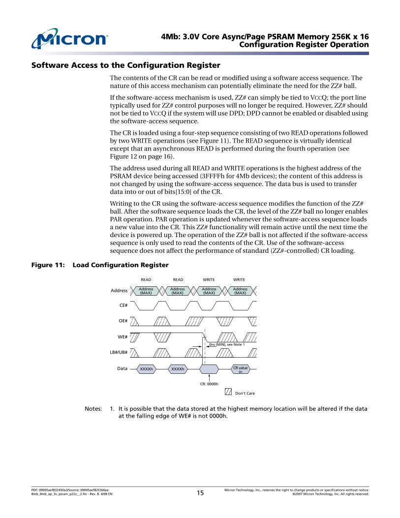
Software Access to the Configuration Register
The contents of the CR can be read or modified using a software access sequence. The nature of this access mechanism can potentially eliminate the need for the ZZ# ball.
If the software-access mechanism is used, ZZ# can simply be tied to VCCQ; the port line typically used for ZZ# control purposes will no longer be required. However, ZZ# should not be tied to VCCQ if the system will use DPD; DPD cannot be enabled or disabled using the software-access sequence.
The CR is loaded using a four-step sequence consisting of two READ operations followed by two WRITE operations (see Figure 11). The READ sequence is virtually identical except that an asynchronous READ is performed during the fourth operation (see Figure 12 on page 16).
The address used during all READ and WRITE operations is the highest address of the PSRAM device being accessed (3FFFFh for 4Mb devices); the content of this address is not changed by using the software-access sequence. The data bus is used to transfer data into or out of bits[15:0] of the CR.
Writing to the CR using the software-access sequence modifies the function of the ZZ# ball. After the software sequence loads the CR, the level of the ZZ# ball no longer enables PAR operation. PAR operation is updated whenever the software-access sequence loads a new value into the CR. This ZZ# functionality will remain active until the next time the device is powered up. The operation of the ZZ# ball is not affected if the software-access sequence is only used to read the contents of the CR. Use of the software-access sequence does not affect the performance of standard (ZZ#-controlled) CR loading.
Figure 11: Load Configuration Register
Notes: 1. It is possible that the data stored at the highest memory location will be altered if the data at the falling edge of WE# is not 0000h.
Address(MAX)
Address(MAX)
Address(MAX)
XXXXh XXXXh
CR: 0000h
CR valuein
Address
CE#
OE#
WE#
LB#/UB#
Data
Don’t Care
READ READ WRITE WRITE
Address(MAX)
0ns (MIN), see Note 1
PDF: 09005aef832450a3/Source: 09005aef82f264aa Micron Technology, Inc., reserves the right to change products or specifications without notice.8mb_4mb_ap_3v_psram_p22z__2.fm - Rev. B 4/08 EN 15 ©2007 Micron Technology, Inc. All rights reserved.
4Mb: 3.0V Core Async/Page PSRAM Memory 256K x 16Configuration Register Operation
Figure 12: Read Configuration Register
Notes: 1. It is possible that the data stored at the highest memory location will be altered if the data at the falling edge of WE# is not 0000h.
Partial-Array Refresh (CR[2:0]) Default = Full-Array Refresh
The PAR bits restrict REFRESH operation to a portion of the total memory array. The refresh options are “full array” and “none of the array.”
Sleep Mode (CR[4]) Default = PAR Enabled, DPD Disabled
The sleep mode bit defines the low-power mode to be entered when ZZ# is driven LOW. If CR[4] = 1, PAR operation is enabled. If CR[4] = 0, DPD operation is enabled. PAR can also be enabled directly by writing to the CR using the software-access sequence. Note that this disables ZZ# initiation of PAR. DPD cannot properly be enabled or disabled using the software-access sequence; DPD should only be enabled or disabled using ZZ# to access the CR.
DPD operation disables all refresh-related activity. This mode is used when the system does not require the storage provided by the PSRAM device. When DPD is enabled, any stored data will become corrupted. When refresh activity has been re-enabled, the PSRAM device will require 150µs to perform an initialization procedure before normal operation can resume. DPD should not be enabled using CR software access.
Page Mode READ Operation (CR[7]) Default = Disabled
The page mode operation bit determines whether page mode READ operations are enabled. In the power-up default state, page mode is disabled.
Address(MAX)
Address(MAX)
Address(MAX)
XXXXh XXXXh CR valueout
Address
CE#
OE#
WE#
LB#/UB#
Data
Don’t Care
READ READ WRITE READ
CR: 0000h
Address(MAX)
0ns (MIN), see Note 1
PDF: 09005aef832450a3/Source: 09005aef82f264aa Micron Technology, Inc., reserves the right to change products or specifications without notice.8mb_4mb_ap_3v_psram_p22z__2.fm - Rev. B 4/08 EN 16 ©2007 Micron Technology, Inc. All rights reserved.
4Mb: 3.0V Core Async/Page PSRAM Memory 256K x 16Electrical Characteristics
Electrical CharacteristicsStresses greater than those listed in Table 3 may cause permanent damage to the device. This is a stress rating only, and functional operation of the device at these or any other conditions above those indicated in the operational sections of this specification is not implied. Exposure to absolute maximum rating conditions for extended periods may affect reliability.
Notes: 1. Input signals may overshoot to VCCQ + 1.0V for periods less than 2ns during transitions.2. Input signals may undershoot to VSS - 1.0V for periods less than 2ns during transitions.3. This parameter is specified with the outputs disabled to avoid external loading effects. The
user must add the current required to drive output capacitance expected in the actual sys-tem.
4. ISB (MAX) values measured with PAR set to FULL ARRAY. To achieve low standby current, all inputs must be driven to VCCQ or VSS. ISB may be slightly higher for up to 500ms after power-up or when entering standby mode.
Table 3: Absolute Maximum Ratings
Parameter Rating
Voltage to any ball except VCC; VCCQ relative to VSS –0.5V to 4.0V or VCCQ + 0.3V (whichever is less)
Voltage on VCC supply relative to VSS –0.2V to +4.0V
Voltage on VCCQ supply relative to VSS –0.2V to +4.0V
Storage temperature –55°C to +150°C
Operating temperature (case)WirelessIndustrial
–30°C to +85°C–40°C to +85°C
Soldering temperature and time10 seconds (solder ball only) 260°C
Table 4: Electrical Characteristics and Operating ConditionsWireless temperature (–30ºC ≤ TC ≤ +85 ºC); Industrial temperature (–40ºC < TC < +85ºC)
Description Conditions Symbol Min Max Unit Notes
Supply voltage VCC 2.7 3.6 V
I/O supply voltage VCCQ 2.7 3.6 V
Input high voltage VIH VCCQ - 0.4 VCCQ + 0.2 V 1
Input low voltage VIL –0.2 +0.4 V 2
Output high voltage IOH = –0.2mA VOH 0.8 VCCQ – V
Output low voltage IOL = 0.2mA VOL – 0.2 VCCQ V
Input leakage current VIN = 0 to VCCQ ILI – 1 µA
Output leakage current OE# = VIH orChip disabled
ILO – 1 µA
Operating CurrentAsynchronous random READ/WRITE
VIN = VCCQ or 0VChip enabled; IOUT = 0
ICC1 -55, -70 – 30 mA 3
Asynchronous page READ ICC1P -55, -70 – 18 mA 3
Standby current VIN = VCCQ or 0VCE# = VCCQ
ISB – 140 µA 4
PDF: 09005aef832450a3/Source: 09005aef82f264aa Micron Technology, Inc., reserves the right to change products or specifications without notice.8mb_4mb_ap_3v_psram_p22z__2.fm - Rev. B 4/08 EN 17 ©2007 Micron Technology, Inc. All rights reserved.
4Mb: 3.0V Core Async/Page PSRAM Memory 256K x 16Electrical Characteristics
Maximum and Typical Standby Currents
Maximum and typical standby currents for the MT45V256KW16PE device are shown in Figure 13.
Figure 13: Typical Refresh Current vs. Temperature
Notes: 1. These parameters are verified in device characterization and are not 100% tested.
Table 5: Deep Power-Down Specifications and Conditions
Description Conditions Symbol Typ Units
Deep power-down VIN = VCCQ or 0V; +25°CZZ# = 0VCR[4] = 0
IZZ 45 µA
Table 6: Capacitance Specifications and Conditions
Description Conditions Symbol Min Max Unit Notes
Input capacitance TC = +25ºC; f = 1 MHz;VIN = 0V
CIN 2.0 6.5 pF 1
Input/output capacitance (DQ) CIO 3.0 6.5 pF 1
–45 –35 –25 –15 –5 5 15 25 35 45 55 65 75 85 95
90
80
70
60
50
40
30
20
10
0
Temperature (°C)
ISB (
µA
)
PAR fullPAR 0
PDF: 09005aef832450a3/Source: 09005aef82f264aa Micron Technology, Inc., reserves the right to change products or specifications without notice.8mb_4mb_ap_3v_psram_p22z__2.fm - Rev. B 4/08 EN 18 ©2007 Micron Technology, Inc. All rights reserved.
4Mb: 3.0V Core Async/Page PSRAM Memory 256K x 16Electrical Characteristics
Figure 14: AC Input/Output Reference Waveform
Notes: 1. AC test inputs are driven at VCCQ for a logic 1 and VSSQ for a logic 0. Input rise and fall times (10% to 90%) < 1.6ns.
2. Input timing begins at VCCQ/2.3. Output timing ends at VCCQ/2.
Figure 15: Output Load Circuit
Notes: 1. Low-Z to High-Z timings are tested with the circuit shown in Figure 15 on page 19. The High-Z timings measure a 100mV transition either from VOH or VOL toward VCCQ/2.
2. High-Z to Low-Z timings are tested with the circuit shown in Figure 15 on page 19. The Low-Z timings measure a 100mV transition away from the High-Z (VCCQ/2) level either toward VOH or VOL.
3. Page mode enabled only.
Table 7: READ Cycle Timing Requirements
Parameter Symbol
-55 -70
Unit NotesMin Max Min Max
Address access time tAA – 55 – 70 ns
Page access time tAPA – 15 – 20 ns
LB#/UB# access time tBA – 55 – 70 ns
LB#/UB# disable to High-Z output tBHZ – 8 – 8 ns 1
LB#/UB# enable to Low-Z output tBLZ 10 – 10 – ns 2
Maximum CE# pulse width tCEM – 8 – 8 µs 3
Chip select access time tCO – 55 – 70 ns
Chip disable to High-Z output tHZ – 8 – 8 ns 1
Chip enable to Low-Z output tLZ 10 – 10 – ns 2
Output enable to valid output tOE – 20 – 20 ns
Output hold from address change tOH 5 – 5 – ns
Output disable to High-Z output tOHZ – 8 – 8 ns 1
Output enable to Low-Z output tOLZ 3 – 3 – ns 2
Page cycle time tPC 20 – 20 – ns
Read cycle time tRC 55 – 70 – ns
Output Test pointsInput1
VCCQ
VSSQ
VCCQ/23 VCCQ/22
DUT VccQ/2
30pF
Test point
50
PDF: 09005aef832450a3/Source: 09005aef82f264aa Micron Technology, Inc., reserves the right to change products or specifications without notice.8mb_4mb_ap_3v_psram_p22z__2.fm - Rev. B 4/08 EN 19 ©2007 Micron Technology, Inc. All rights reserved.
4Mb: 3.0V Core Async/Page PSRAM Memory 256K x 16Electrical Characteristics
Notes: 1. High-Z to Low-Z timings are tested with the circuit shown in Figure 15 on page 19. The Low-Z timings measure a 100mV transition away from the High-Z (VCCQ/2) level either toward VOH or VOL.
2. Low-Z to High-Z timings are tested with the circuit shown in Figure 15 on page 19. The High-Z timings measure a 100mV transition either from VOH or VOL toward VCCQ/2.
3. WE# LOW time must be limited to tCEM (8µs).
Table 8: WRITE Cycle Timing Requirements
Parameter Symbol
-55 -70
Unit NotesMin Max Min Max
Address setup time tAS 0 – 0 – ns
Address valid to end of write tAW 45 – 70 – ns
Byte select to end of write tBW 45 – 70 – ns
CE# HIGH time during write tCPH 5 – 5 – ns
Chip enable to end of write tCW 45 – 70 – ns
Data hold from write time tDH 0 – 0 – ns
Data write setup time tDW 23 – 23 – ns
Chip enable to Low-Z output tLZ 10 – 10 – ns 1
End write to Low-Z output tOW 5 – 5 – ns 1
WRITE cycle time tWC 55 – 70 – ns
Write to High-Z output tWHZ – 8 – 8 ns 2
Write pulse width tWP 35 – 46 – ns 3
Write pulse width HIGH tWPH 10 – 10 – ns
Write recovery time tWR 0 – 0 – ns
Table 9: Load Configuration Register Timing Requirements
Description Symbol
-55 -70
UnitMin Max Min Max
Address setup time tAS 0 – 0 – ns
Address valid to end of write tAW 45 – 70 – ns
Chip deselect to ZZ# LOW tCDZZ 5 – 5 – ns
Chip enable to end of write tCW 45 – 70 – ns
Write cycle time tWC 55 – 70 – ns
Write pulse width tWP 35 – 46 – ns
Write recovery time tWR 0 – 0 – ns
ZZ# LOW to WE# LOW tZZWE 10 500 10 500 ns
Table 10: Deep Power-Down Timing Requirements
Description Symbol
-55 -70
UnitMin Max Min Max
Chip deselect to ZZ# LOW tCDZZ 5 – 5 – ns
Deep power-down recovery tR 150 – 150 – µs
Minimum ZZ# pulse width tZZ (MIN) 10 – 10 – µs
PDF: 09005aef832450a3/Source: 09005aef82f264aa Micron Technology, Inc., reserves the right to change products or specifications without notice.8mb_4mb_ap_3v_psram_p22z__2.fm - Rev. B 4/08 EN 20 ©2007 Micron Technology, Inc. All rights reserved.
4Mb: 3.0V Core Async/Page PSRAM Memory 256K x 16Timing Diagrams
Timing Diagrams
Figure 16: Power-Up Initialization Period
Figure 17: Load Configuration Register
Figure 18: Deep Power-Down Entry and Exit
Table 11: Initialization Timing Parameters
Parameter Symbol Min Max Unit
Initialization period (required before normal operations) tPU – 150 µs
Device ready fornormal operation
Vcc, VccQ = 2.7VtPU
Vcc (MIN)
Address
ZZ#
tWC
tAW tWR
tAS
CE#
LB#/UB#
tZZWE
Don’t Care
WE#
tWP
tCDZZ
OPCODE
tCW
OE#
ZZ#
CE#
tZZ (MIN)
Don’t Care
tCDZZ
tR
Device ready for normal operation
PDF: 09005aef832450a3/Source: 09005aef82f264aa Micron Technology, Inc., reserves the right to change products or specifications without notice.8mb_4mb_ap_3v_psram_p22z__2.fm - Rev. B 4/08 EN 21 ©2007 Micron Technology, Inc. All rights reserved.
4Mb: 3.0V Core Async/Page PSRAM Memory 256K x 16Timing Diagrams
Figure 19: Single READ Operation (WE# = VIH)
Figure 20: Page Mode READ Operation (WE# = VIH)
Address
OE#
tRC
tAA
Data out
CE#
LB#/UB#
tOLZ
Don’t Care Undefined
High-Z High-Z Valid data
tOHZ
tBA tBHZ
tHZ
tBLZ
tCO
Valid address
tOE
tLZ
Address
A[17:4]
OE#
tAA
Data out
CE#
LB#/UB#
tOLZ
tLZ
Don’t Care Undefined
High-Z High-ZValiddata
tOHZ
tBAtBHZ
tHZtCEM
tBLZ
tCO
Address
A[3:0]
tRC
tOH
tPC
Valid address
tAPA
tOE
Validdata
Validdata
Validdata
PDF: 09005aef832450a3/Source: 09005aef82f264aa Micron Technology, Inc., reserves the right to change products or specifications without notice.8mb_4mb_ap_3v_psram_p22z__2.fm - Rev. B 4/08 EN 22 ©2007 Micron Technology, Inc. All rights reserved.
4Mb: 3.0V Core Async/Page PSRAM Memory 256K x 16Timing Diagrams
Figure 21: WRITE Cycle (WE# Control)
Figure 22: WRITE Cycle (CE# Control)
Address
WE#
tWC
tAW tWR
Data in
CE#
LB#/UB#
tBW
tWHZ tOW
tDH tDW
tAS tWP tWPH
Don’t Care
High-Z Data out
Valid data
tCW
OE#
Valid address
Address
WE#
tWC
tAW
tCW
tWR
tCPH
Data in
CE#
LB#/UB#
tBW
tWHZ tLZ
tAS
tDH tDW
tWP
Don’t Care
High-Z Data out
Valid data
Valid address
OE#
PDF: 09005aef832450a3/Source: 09005aef82f264aa Micron Technology, Inc., reserves the right to change products or specifications without notice.8mb_4mb_ap_3v_psram_p22z__2.fm - Rev. B 4/08 EN 23 ©2007 Micron Technology, Inc. All rights reserved.
4Mb: 3.0V Core Async/Page PSRAM Memory 256K x 16Timing Diagrams
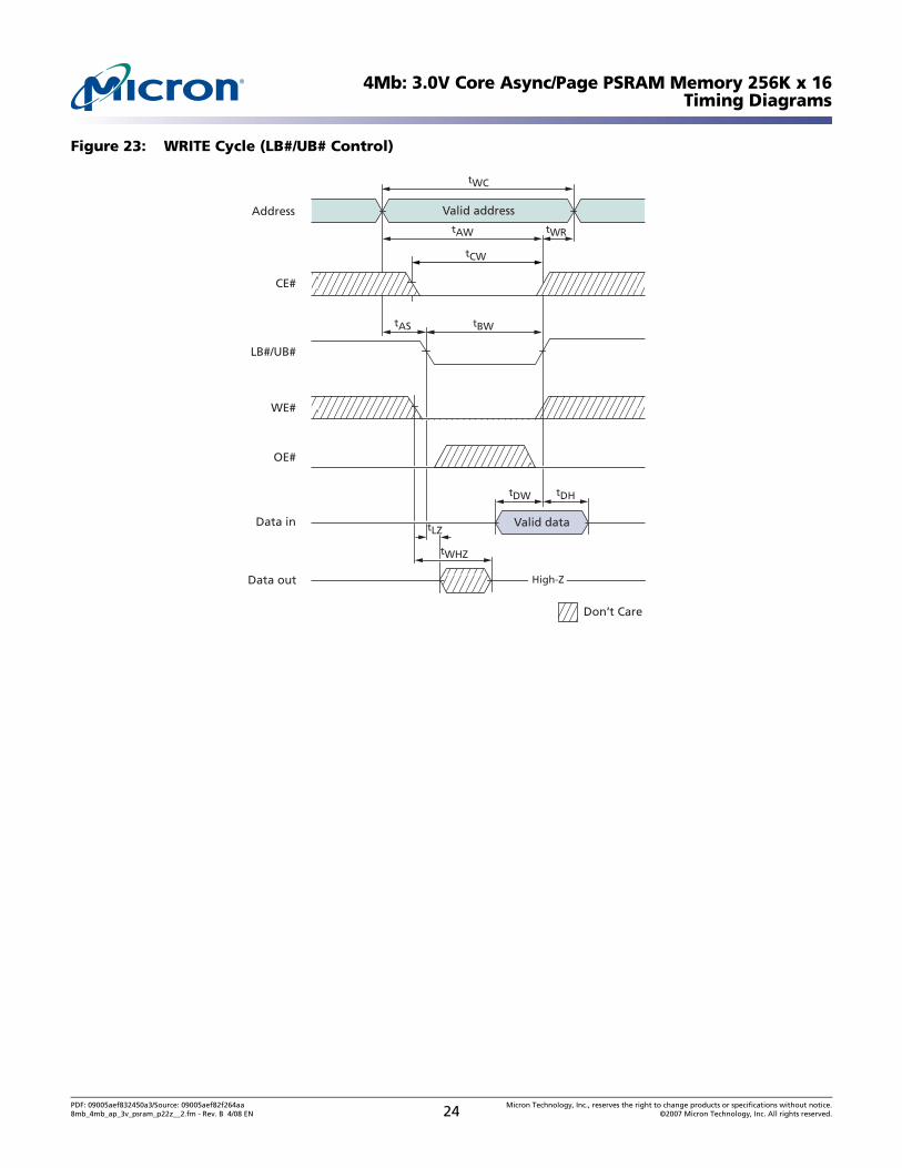
Figure 23: WRITE Cycle (LB#/UB# Control)
Address
WE#
tWC
tAW tWR
Data in
CE#
LB#/UB#
tBW
tWHZ
tDH
tAS
tDW
tLZ
Don’t Care
Data out
Valid data
Valid address
tCW
OE#
High-Z
PDF: 09005aef832450a3/Source: 09005aef82f264aa Micron Technology, Inc., reserves the right to change products or specifications without notice.8mb_4mb_ap_3v_psram_p22z__2.fm - Rev. B 4/08 EN 24 ©2007 Micron Technology, Inc. All rights reserved.
4Mb: 3.0V Core Async/Page PSRAM Memory 256K x 16Package Dimensions
Package Dimensions
Figure 24: 48-Ball VFBGA
Notes: 1. All dimensions are in millimeters.2. Package width and length do not include mold protrusion; allowable mold protrusion is
0.25mm per side.3. The MT45V256KW16PE uses “green” packaging.
Ball A1 ID
1.00 MAX
4.00 ±0.05
3.00 ±0.05 1.875
6.00 ±0.10
C L
C L
Solder ball material: 96.5% Sn, 3% Ag, 0.5% Cu
Mold compound: epoxy novolacSubstrate material: plastic laminate
0.75 TYP
0.75 TYP
8.00 ±0.10 5.25
2.625
Ball A1Ball A1 ID
3.75
0.70 ±0.05
Seatingplane
0.10 A
A
Ball A6
Dimensions applyto solder ballspost-reflow.Pre-reflow balldiameter is 0.35on a 0.30 SMDball pad.
48X Ø0.37
®
8000 S. Federal Way, P.O. Box 6, Boise, ID 83707-0006, Tel: [email protected] www.micron.com Customer Comment Line: 800-932-4992
Micron, the M logo, and the Micron logo are trademarks of Micron Technology, Inc. CellularRAM is a trademark of Micron Technology, Inc., inside the U.S. and a trademark of Qimonda AG outside the U.S. All other trademarks are the property of their respective owners. This data
sheet contains minimum and maximum limits specified over the complete power supply and temperature range for production devices. Although considered final, these specifications are subject to change, as further product development and data characterization some-
times occur.
PDF: 09005aef832450a3/Source: 09005aef82f264aa Micron Technology, Inc., reserves the right to change products or specifications without notice.8mb_4mb_ap_3v_psram_p22z__2.fm - Rev. B 4/08 EN 25 ©2007 Micron Technology, Inc. All rights reserved.
4Mb: 3.0V Core Async/Page PSRAM Memory 256K x 16Revision History
Revision HistoryRev. B, Production . . . . . . . . . . . . . . . . . . . . . . . . . . . . . . . . . . . . . . . . . . . . . . . . . . . . . . . . . . . . . . . . . . . . . . . . . . . . . . . . . . . 4/08
• Changed to production status.
Rev. A, Preliminary . . . . . . . . . . . . . . . . . . . . . . . . . . . . . . . . . . . . . . . . . . . . . . . . . . . . . . . . . . . . . . . . . . . . . . . . . . . . . . . . . . . 2/08• Initial release.
PDF: 09005aef832450a3/Source: 09005aef82f264aa Micron Technology, Inc., reserves the right to change products or specifications without notice.8mb_4mb_ap_3v_psram_p22z__2.fm - Rev. B 4/08 EN 26 ©2007 Micron Technology, Inc. All rights reserved.