Embed Size (px)
Citation preview
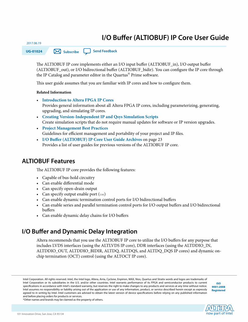
I/O Buffer (ALTIOBUF) IP Core User Guide2017.06.19
UG-01024 Subscribe Send Feedback
The ALTIOBUF IP core implements either an I/O input buffer (ALTIOBUF_in), I/O output buffer(ALTIOBUF_out), or I/O bidirectional buffer (ALTIOBUF_bidir). You can configure the IP core throughthe IP Catalog and parameter editor in the Quartus® Prime software.
This user guide assumes that you are familiar with IP cores and how to configure them.
Related Information
• Introduction to Altera FPGA IP CoresProvides general information about all Altera FPGA IP cores, including parameterizing, generating,upgrading, and simulating IP cores.
• Creating Version-Independent IP and Qsys Simulation ScriptsCreate simulation scripts that do not require manual updates for software or IP version upgrades.
• Project Management Best PracticesGuidelines for efficient management and portability of your project and IP files.
• I/O Buffer (ALTIOBUF) IP Core User Guide Archives on page 23Provides a list of user guides for previous versions of the ALTIOBUF IP core.
ALTIOBUF FeaturesThe ALTIOBUF IP core provides the following features:
• Capable of bus-hold circuitry• Can enable differential mode• Can specify open-drain output• Can specify output enable port (oe)• Can enable dynamic termination control ports for I/O bidirectional buffers• Can enable series and parallel termination control ports for I/O output buffers and I/O bidirectional
buffers• Can enable dynamic delay chains for I/O buffers
I/O Buffer and Dynamic Delay IntegrationAltera recommends that you use the ALTIOBUF IP core to utilize the I/O buffers for any purpose thatincludes LVDS interfaces (using the ALTLVDS IP core), DDR interfaces (using the ALTDDIO_IN,ALTDDIO_OUT, ALTDDIO_BIDIR, ALTDQ, ALTDQS, and ALTDQ_DQS IP cores) and dynamic on-chip termination (OCT) control (using the ALTOCT IP core).
Intel Corporation. All rights reserved. Intel, the Intel logo, Altera, Arria, Cyclone, Enpirion, MAX, Nios, Quartus and Stratix words and logos are trademarks ofIntel Corporation or its subsidiaries in the U.S. and/or other countries. Intel warrants performance of its FPGA and semiconductor products to currentspecifications in accordance with Intel's standard warranty, but reserves the right to make changes to any products and services at any time without notice.Intel assumes no responsibility or liability arising out of the application or use of any information, product, or service described herein except as expresslyagreed to in writing by Intel. Intel customers are advised to obtain the latest version of device specifications before relying on any published informationand before placing orders for products or services.*Other names and brands may be claimed as the property of others.
ISO9001:2008Registered
www.altera.com101 Innovation Drive, San Jose, CA 95134
ALTIOBUF Common ApplicationThe I/O buffers have standard capabilities such as bus-hold circuitry, differential mode, open-drain output,and output enable port.
One of the key applications for this IP core is to have more direct termination control of the buffers. Byenabling series and parallel termination control ports for the I/O output buffers and I/O bidirectionalbuffers, you can connect these ports to the ALTOCT IP core to enable dynamic calibration for on-chiptermination.
The additional dynamic termination control ports allow control when series termination or paralleltermination are enabled for bidirectional buffers. Parallel termination needs to only be enabled when thebidirectional I/O is receiving input. Otherwise, it needs to be disabled so that the output performance andpower dissipation is optimal.
Another key application for this IP core is for dynamic delay chain in the I/O buffer. Dynamic I/O delayallows implementing automatic deskew, especially for memory interfaces, such as DDR3, which is handledby the memory interface intellectual property (IP). You need to dynamically deskew and not calculatemanually because much of the skew can come from the I/O buffers of either the FPGA or the other devicethe FPGA is interfacing with (for example, memory). Even if the trace lengths are matched, there can stillbe electrical skew in the system. Also, this skew changes and can change from device to device. Having theability to deskew from the fabric allows you to remove uncertainties that would have to be considered inthe timing budget. This allows you to gain more timing margin, which allows higher frequencies.
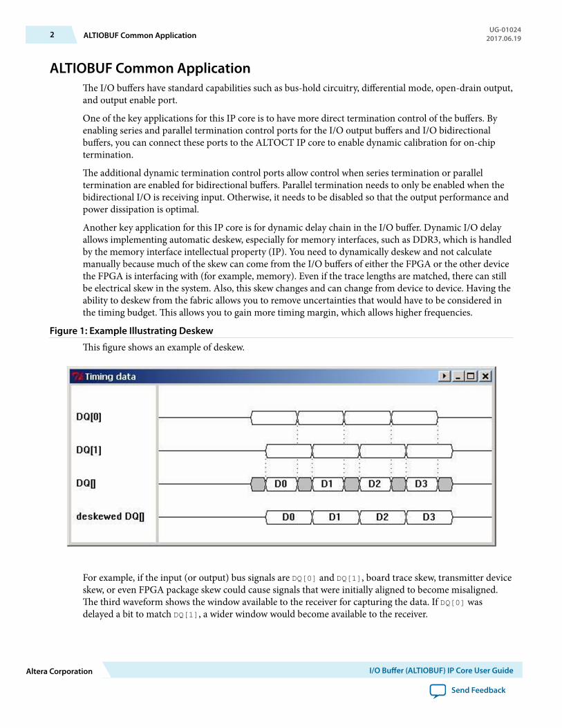
Figure 1: Example Illustrating Deskew
This figure shows an example of deskew.
For example, if the input (or output) bus signals are DQ[0] and DQ[1], board trace skew, transmitter deviceskew, or even FPGA package skew could cause signals that were initially aligned to become misaligned.The third waveform shows the window available to the receiver for capturing the data. If DQ[0] wasdelayed a bit to match DQ[1], a wider window would become available to the receiver.
2 ALTIOBUF Common ApplicationUG-01024
2017.06.19
Altera Corporation I/O Buffer (ALTIOBUF) IP Core User Guide
Send Feedback
Note: The deskew delay chains are not meant to find the middle of a data valid window, but just to deskewthe incoming (or outgoing) data to widen the overall window for a bus of inputs (or outputs). To dothis, you only need to align just one edge (for example, the left edge) of the data valid window of allthe pins.
To find the left and right edges of the data valid window, you need to do coarser adjustments (one possiblemethod is to use the new phase adjustment functionality of the PLL (ALTPLL IP core). The range of thedeskew delay chains is only designed to compensate for a reasonable amount of board and package/layoutskew.
Related InformationALTOCT IP Core User GuideProvides information about connecting the ALTIOBUF ports to ALTOCT IP core.
ALTIOBUF ParametersThis table lists the options ALTIOBUF IP core parameters.
Table 1: ALTIOBUF IP Core Parameters: General Tab
Parameter Description
Currently selected device family: Specify the device family you want to use.
How do you want to configure thismodule?
Specify whether it is an input buffer, output buffer, or bidirec‐tional buffer.
What is the number of buffers to beinstantiated?
Specify the number of buffers to be used. This defines the sizeof the buffer.
Use bus hold circuitry If enabled, the bus-hold circuitry can weakly hold the signalon an I/O pin at its last-driven state. Available in input buffer,output buffer, or bidirectional buffer.
Use differential mode If enabled, datain/datain_b is used for input buffers, bothdataout/dataout_b are used for output buffers, and bothdataio/dataio_b are used for bidirectional buffers.
Use open drain output If enabled, the open drain output enables the device to providesystem-level control signals (for example, interrupt and write-enable signals) that can be asserted by multiple devices in yoursystem. This option is only available for output buffers andbidirectional buffers.
Use output enable port(s) If enabled, there is a port used to control when the output isenabled. This option is only available for output buffers andbidirectional buffers.
UG-010242017.06.19 ALTIOBUF Parameters 3
I/O Buffer (ALTIOBUF) IP Core User Guide Altera Corporation
Send Feedback
Parameter Description
Use dynamic termination control(s) If enabled, this port receives the command to select either Rscode (when input value = low) or Rt code (when input value =high) from the core. Only enable Rt when the bi-directional I/O is receiving input. Otherwise, it needs to be disabled so thatthe output performance and power dissipation is optimal. Thisoption is available only for input and bidirectional buffers.
An error is issued if parallel termination (Rt) is on anddynamic termination control is not connected on a bidir pin.An error is issued if parallel termination (Rt) is off anddynamic termination control is connected on an input orbidirectional pin.
Note that two I/Os in the same dynamic termination controlgroup needs to have the same dynamic termination controlsignal. If the I/Os have separate dynamic termination controlsignals, the Quartus Prime software produces a fitting error. Adynamic termination control group is a group of pins thatshare the same physical dynamic termination control signal onthe chip.
This option is not available in Cyclone® III, Cyclone IV, andCyclone 10 LP devices.
Use series and parallel terminationcontrols
If enabled, this allows the series and parallel terminationcontrol ports to be used. These ports can then be connected totermination logic blocks to receive the Rs or Rt code from thetermination logic blocks.
This option is only available for output buffers and bidirec‐tional buffers. The series and parallel termination controlports are 14-bit wide for series or parallel termination.
For Cyclone III, Cyclone IV, Cyclone 10 LP, and Cyclone Vdevices, this option is available for output buffers and bidirec‐tional buffers, but not for input buffers. Only series termina‐tion is available. The series termination control ports are 16-bit wide. The width of these ports increases depending on theamount of buffers instantiated.
Use left shift series termination control If enabled, you can use the left shift series termination controlto get the calibrated OCT Rs with half of the impedance valueof the external reference resistors connected to RUP and RDNpins. This option is useful in applications which required both25-Ω and 50-Ω calibrated OCT Rs at the same Vccio. For moreinformation, refer to I/O features chapter of the respectivedevice handbooks.
4 ALTIOBUF ParametersUG-01024
2017.06.19
Altera Corporation I/O Buffer (ALTIOBUF) IP Core User Guide
Send Feedback
Table 2: ALTIOBUF Parameters: Dynamic Delay Chains Tab
Parameter Description
Enable input buffer dynamic delay chain If enabled, the input or bidirectional buffer incorporates theuser-driven dynamic delay chain in the IP core; that is, theIO_CONFIG and the input delay cell. Additional input ports areenabled: io_config_clk, io_config_clkena, io_config_update, and io_config_datain.
This option is not available for Cyclone III, Cyclone IV, andCyclone 10 LP devices.
Enable output buffer dynamic delay chain1
If enabled, the output or bidirectional buffer incorporates theuser-driven dynamic delay chain in the IP core; that is, theIO_CONFIG and the first output delay cell. Additional inputports are enabled: io_config_clk, io_config_clkena, io_config_update, and io_config_datain.
This option is not available for Cyclone III, Cyclone IV, andCyclone 10 LP devices.
Enable output buffer dynamic delay chain2
If enabled, the output buffer or bidirectional buffer incorpo‐rates a user-driven dynamic delay chain in the IP core; that is,the IO_CONFIG and the second output delay cell. Additionalinput ports are enabled: io_config_clk, io_config_clkena,io_config_update, and io_config_datain.
This option is not available for Cyclone III, Cyclone IV, andCyclone 10 LP devices.
Create a ‘clkena’ port If enabled, there is a port used to control when the configura‐tion clock is enabled. This option is not available for CycloneIII, Cyclone IV, and Cyclone 10 LP devices.
Using the Port and Parameter DefinitionsInstead of using the parameter editor GUI, you can instantiate the IP core directly in your Verilog HDL,VHDL, or AHDL code by calling the IP core and setting its parameters as you would any other module,component, or subdesign.
Related InformationALTIOBUF References on page 11
ALTIOBUF Functional Description
UG-010242017.06.19 Using the Port and Parameter Definitions 5
I/O Buffer (ALTIOBUF) IP Core User Guide Altera Corporation
Send Feedback
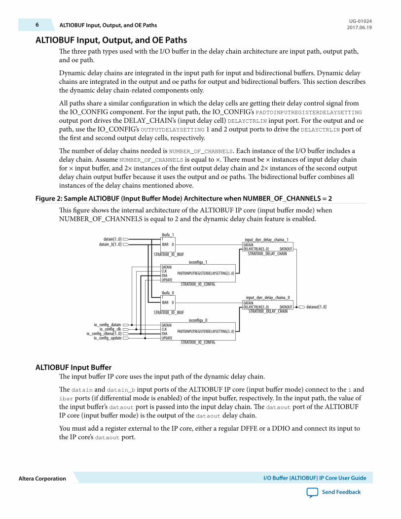
ALTIOBUF Input, Output, and OE PathsThe three path types used with the I/O buffer in the delay chain architecture are input path, output path,and oe path.
Dynamic delay chains are integrated in the input path for input and bidirectional buffers. Dynamic delaychains are integrated in the output and oe paths for output and bidirectional buffers. This section describesthe dynamic delay chain-related components only.
All paths share a similar configuration in which the delay cells are getting their delay control signal fromthe IO_CONFIG component. For the input path, the IO_CONFIG’s PADTOINPUTREGISTERDELAYSETTINGoutput port drives the DELAY_CHAIN’s (input delay cell) DELAYCTRLIN input port. For the output and oepath, use the IO_CONFIG’s OUTPUTDELAYSETTING 1 and 2 output ports to drive the DELAYCTRLIN port ofthe first and second output delay cells, respectively.
The number of delay chains needed is NUMBER_OF_CHANNELS. Each instance of the I/O buffer includes adelay chain. Assume NUMBER_OF_CHANNELS is equal to ×. There must be × instances of input delay chainfor × input buffer, and 2× instances of the first output delay chain and 2× instances of the second outputdelay chain output buffer because it uses the output and oe paths. The bidirectional buffer combines allinstances of the delay chains mentioned above.
Figure 2: Sample ALTIOBUF (Input Buffer Mode) Architecture when NUMBER_OF_CHANNELS = 2
This figure shows the internal architecture of the ALTIOBUF IP core (input buffer mode) whenNUMBER_OF_CHANNELS is equal to 2 and the dynamic delay chain feature is enabled.
STRATIXIII_DELAY_CHAIN
STRATIXIII_DELAY_CHAINdataout[1..0]
input_dyn_delay_chaina_1DATAINDELAYCTRLIN[3..0] DATAOUT
input_dyn_delay_chaina_0DATAINDELAYCTRLIN[3..0] DATAOUT
STRATIXIII_IO_IBUF
ibufa_1IIBAR O
ioconfiga_1
STRATIXIII_IO_CONFIG
DATAINCLKENA PADTOINPUTREGISTERDELAYSETTING[3..0]
UPDATE
io_config_datainio_config_clk
io_config_clkena[1..0]io_config_update
datain[1..0]datain_b[1..0]
STRATIXIII_IO_IBUF
ibufa_0IIBAR O
ioconfiga_0
STRATIXIII_IO_CONFIG
DATAINCLKENA PADTOINPUTREGISTERDELAYSETTING[3..0]
UPDATE
ALTIOBUF Input BufferThe input buffer IP core uses the input path of the dynamic delay chain.
The datain and datain_b input ports of the ALTIOBUF IP core (input buffer mode) connect to the i andibar ports (if differential mode is enabled) of the input buffer, respectively. In the input path, the value ofthe input buffer’s dataout port is passed into the input delay chain. The dataout port of the ALTIOBUFIP core (input buffer mode) is the output of the dataout delay chain.
You must add a register external to the IP core, either a regular DFFE or a DDIO and connect its input tothe IP core’s dataout port.
6 ALTIOBUF Input, Output, and OE PathsUG-01024
2017.06.19
Altera Corporation I/O Buffer (ALTIOBUF) IP Core User Guide
Send Feedback
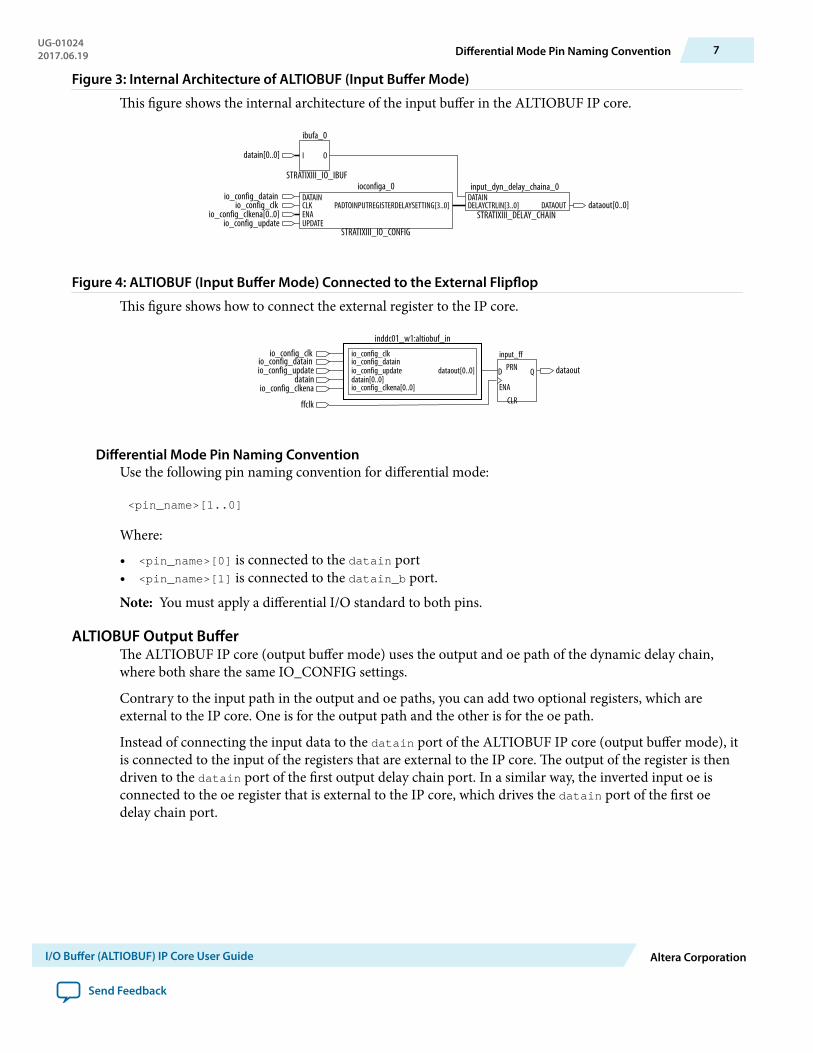
Figure 3: Internal Architecture of ALTIOBUF (Input Buffer Mode)
This figure shows the internal architecture of the input buffer in the ALTIOBUF IP core.
STRATIXIII_IO_IBUF
ibufa_0
I Odatain[0..0]
io_config_datainio_config_clk
ioconfiga_0
STRATIXIII_IO_CONFIG
io_config_clkena[0..0]io_config_update
DATAINCLKENA
PADTOINPUTREGISTERDELAYSETTING[3..0]
UPDATESTRATIXIII_DELAY_CHAIN
input_dyn_delay_chaina_0DATAINDELAYCTRLIN[3..0] DATAOUT dataout[0..0]
Figure 4: ALTIOBUF (Input Buffer Mode) Connected to the External Flipflop
This figure shows how to connect the external register to the IP core.
io_config_datainio_config_clk
inddc01_w1:altiobuf_in
datainio_config_clkena
io_config_update
ffclk
dataout
io_config_clkio_config_datainio_config_update dataout[0..0]datain[0..0]io_config_clkena[0..0]
PRN
CLR
D Q
input_ff
ENA
Differential Mode Pin Naming ConventionUse the following pin naming convention for differential mode:
<pin_name>[1..0]
Where:
• <pin_name>[0] is connected to the datain port• <pin_name>[1] is connected to the datain_b port.
Note: You must apply a differential I/O standard to both pins.
ALTIOBUF Output BufferThe ALTIOBUF IP core (output buffer mode) uses the output and oe path of the dynamic delay chain,where both share the same IO_CONFIG settings.
Contrary to the input path in the output and oe paths, you can add two optional registers, which areexternal to the IP core. One is for the output path and the other is for the oe path.
Instead of connecting the input data to the datain port of the ALTIOBUF IP core (output buffer mode), itis connected to the input of the registers that are external to the IP core. The output of the register is thendriven to the datain port of the first output delay chain port. In a similar way, the inverted input oe isconnected to the oe register that is external to the IP core, which drives the datain port of the first oedelay chain port.
UG-010242017.06.19 Differential Mode Pin Naming Convention 7
I/O Buffer (ALTIOBUF) IP Core User Guide Altera Corporation
Send Feedback
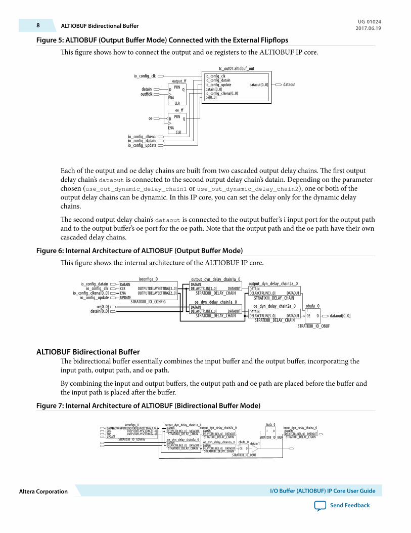
Figure 5: ALTIOBUF (Output Buffer Mode) Connected with the External Flipflops
This figure shows how to connect the output and oe registers to the ALTIOBUF IP core.
datain
io_config_clktc_out01:altiobuf_out
oe
outffclk
dataout
io_config_clkio_config_datainio_config_update dataout[0..0]datain[0..0]io_config_clkena[0..0]
PRN
CLR
D Q
output_ff
ENA
PRN
CLR
D Q
oe_ff
ENA
oe[0..0]
io_config_datainio_config_clkena
io_config_update
Each of the output and oe delay chains are built from two cascaded output delay chains. The first outputdelay chain’s dataout is connected to the second output delay chain’s datain. Depending on the parameterchosen (use_out_dynamic_delay_chain1 or use_out_dynamic_delay_chain2), one or both of theoutput delay chains can be dynamic. In this IP core, you can set the delay only for the dynamic delaychains.
The second output delay chain’s dataout is connected to the output buffer’s i input port for the output pathand to the output buffer’s oe port for the oe path. Note that the output path and the oe path have their owncascaded delay chains.
Figure 6: Internal Architecture of ALTIOBUF (Output Buffer Mode)
This figure shows the internal architecture of the ALTIOBUF IP core.
io_config_datainio_config_clk
ioconfiga_0
STRATIXIII_IO_CONFIG
STRATIXIII_DELAY_CHAINSTRATIXIII_DELAY_CHAIN
STRATIXIII_DELAY_CHAINSTRATIXIII_DELAY_CHAIN
STRATIXIII_IO_OBUF
io_config_clkena[0..0]io_config_update
dataout[0..0]
oe[0..0]datain[0..0]
DATAINCLKENA
OUTPUTDELAYSETTING[3..0]OUTPUTDELAYSETTING[2..0]
UPDATE
output_dyn_delay_chain2a_0output_dyn_delay_chain1a_0DATAINDELAYCTRLIN[3..0] DATAOUT
oe_dyn_delay_chain1a_0DATAINDELAYCTRLIN[3..0] DATAOUT
obufa_0
DATAINDELAYCTRLIN[3..0] DATAOUT
oe_dyn_delay_chain2a_0DATAINDELAYCTRLIN[3..0]
IOEDATAOUT O
ALTIOBUF Bidirectional BufferThe bidirectional buffer essentially combines the input buffer and the output buffer, incorporating theinput path, output path, and oe path.
By combining the input and output buffers, the output path and oe path are placed before the buffer andthe input path is placed after the buffer.
Figure 7: Internal Architecture of ALTIOBUF (Bidirectional Buffer Mode)
ioconfiga_0
STRATIXIII_IO_CONFIGSTRATIXIII_DELAY_CHAIN
STRATIXIII_DELAY_CHAIN
STRATIXIII_DELAY_CHAINSTRATIXIII_DELAY_CHAIN
STRATIXIII_IO_OBUF
DATAINCLKENA
OUTPUTDELAYSETTING[3..0]PADTOINPUTREGISTERDELAYSETTING[3..0]
OUTPUTDELAYSETTING[2..0]UPDATE
output_dyn_delay_chain2a_0output_dyn_delay_chain1a_0
DATAINDELAYCTRLIN[3..0] DATAOUT
oe_dyn_delay_chain1a_0DATAINDELAYCTRLIN[3..0] DATAOUT
obufa_0
DATAINDELAYCTRLIN[3..0] DATAOUT
oe_dyn_delay_chain2a_0DATAINDELAYCTRLIN[3..0]
IOEDATAOUT O
STRATIXIII_IO_IBUF
ibufa_0
I O
STRATIXIII_DELAY_CHAIN
input_dyn_delay_chaina_0DATAINDELAYCTRLIN[3..0] DATAOUT
dataio 1
8 ALTIOBUF Bidirectional BufferUG-01024
2017.06.19
Altera Corporation I/O Buffer (ALTIOBUF) IP Core User Guide
Send Feedback
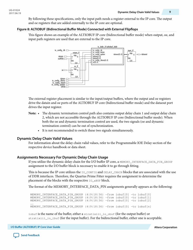
By following these specifications, only the input path needs a register external to the IP core. The outputand oe registers that are added externally to the IP core are optional.
Figure 8: ALTIOBUF (Bidirectional Buffer Mode) Connected with External Flipflops
This figure shows an example of the ALTIOBUF IP core (bidirectional buffer mode) when output, oe, andinput path registers are used that are external to the IP core.
datain
io_config_clktc_bidir_01:altiobuf_bidir
oe
outffclk
dataout
io_config_clkio_config_datainio_config_update dataout[0..0]datain[0..0]dataio[0..0]
PRN
CLR
D Q
output_ff
ENA
PRN
CLR
D Q
oe_ff
ENA
io_config_clkena[0..0]
io_config_clkenadataio
io_config_datainio_config_update
inffclk
oe[0..0]
PRN
CLR
D Q
input_ff
ENA
The external register placement is similar to the input/output buffers, where the output and oe registersdrive the datain and oe ports of the ALTIOBUF IP core (bidirectional buffer mode) and the dataout portdrives the input register.
Note: • The dynamic termination control path also contains output delay chain 1 and output delay chain2, which are not accessible through the ALTIOBUF IP core (bidirectional buffer mode). Whenboth the oe and dynamic termination control are used, the two signals (oe and dynamictermination control) can be out of synchronization.
• It is not recommended to switch these two signals simultaneously.
Dynamic Delay Chain Valid ValuesFor information about the delay chain valid values, refer to the Programmable IOE Delay section of therespective device handbook or data sheet.
Assignments Necessary For Dynamic Delay Chain UsageIf you utilize the dynamic delay chain for the I/O buffer IP core, a MEMORY_INTERFACE_DATA_PIN_GROUPassignment to the I/O buffer block is necessary to enable it to go through fitting.
This is because the IP core utilizes the IO_CONFIG and DELAY_CHAIN blocks that are associated with the useof DDR interfaces. Therefore, the Quartus Prime Fitter requires the assignment to determine theplacement of the blocks with the respective IO_xBUF block.
The format of the MEMORY_INTERFACE_DATA_PIN assignments generally appears as the following:
MEMORY_INTERFACE_DATA_PIN_GROUP 4|9|18|36 -from iobuf[0] -to iobuf[0]MEMORY_INTERFACE_DATA_PIN_GROUP 4|9|18|36 -from iobuf[0] -to iobuf[1]MEMORY_INTERFACE_DATA_PIN_GROUP 4|9|18|36 -from iobuf[0] -to iobuf[2]….MEMORY_INTERFACE_DATA_PIN_GROUP 4|9|18|36 -from iobuf[0] -to iobuf[n]
iobuf is the name of the buffer, either a stratixiii_io_obuf (for the output buffer) orstratixiii_io_ibuf (for the input buffer). For the bidirectional buffer, either one is acceptable.
UG-010242017.06.19 Dynamic Delay Chain Valid Values 9
I/O Buffer (ALTIOBUF) IP Core User Guide Altera Corporation
Send Feedback
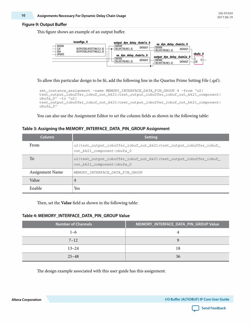
Figure 9: Output Buffer
This figure shows an example of an output buffer.
ioconfiga_0
obufa_0
output_dyn_delay_chain1a_0
oe_dyn_delay_chain1a_0 output_dyn_delay_chain2a_0
oe_dyn_delay_chain2a_0DATAINCLKENAUPDATE
OUTPUTDELAYSETTING1[3..0]OUTPUTDELAYSETTING2[2..0]
DATAINDELAYCTRLIN[3..0] DATAOUT
DATAINDELAYCTRLIN[3..0]
IOE
ODATAOUT
DATAINDELAYCTRLIN[3..0] DATAOUT
DATAINDELAYCTRLIN[3..0] DATAOUT
To allow this particular design to be fit, add the following line in the Quartus Prime Setting File (.qsf):
set_instance_assignment -name MEMORY_INTERFACE_DATA_PIN_GROUP 4 -from "u2|test_output_iobuffer_iobuf_out_kk21:test_output_iobuffer_iobuf_out_kk21_component|obufa_0" -to "u2|test_output_iobuffer_iobuf_out_kk21:test_output_iobuffer_iobuf_out_kk21_component|obufa_0"
You can also use the Assignment Editor to set the column fields as shown in the following table:
Table 3: Assigning the MEMORY_INTERFACE_DATA_PIN_GROUP Assignment
Column Setting
From u2|test_output_iobuffer_iobuf_out_kk21:test_output_iobuffer_iobuf_
out_kk21_component|obufa_0
To u2|test_output_iobuffer_iobuf_out_kk21:test_output_iobuffer_iobuf_
out_kk21_component|obufa_0
Assignment Name MEMORY_INTERFACE_DATA_PIN_GROUP
Value 4
Enable Yes
Then, set the Value field as shown in the following table:
Table 4: MEMORY_INTERFACE_DATA_PIN_GROUP Value
Number of Channels MEMORY_INTERFACE_DATA_PIN_GROUP Value
1–6 4
7–12 9
13–24 18
25–48 36
The design example associated with this user guide has this assignment.
10 Assignments Necessary For Dynamic Delay Chain UsageUG-01024
2017.06.19
Altera Corporation I/O Buffer (ALTIOBUF) IP Core User Guide
Send Feedback
Related InformationALTDQ_DQS2 IP Core User GuideProvides the I/O configuration block bit sequence for Arria® V, Cyclone V, and Stratix® V devices
ALTIOBUF ReferencesProvides the signals, parameters, Verilog HDL prototype, and VHDL component declaration forALTIOBUF IP core.
Related InformationUsing the Port and Parameter Definitions on page 5
ALTIOBUF Signals and Parameters: As Input Buffer
Table 5: ALTIOBUF (As Input Buffer) Input Ports
This table lists the input ports for the ALTIOBUF IP core (as input buffer).Name Required Description
datain[] Yes The input buffer normal data input port.
Input port [NUMBER_OF_CHANNELS - 1..0] wide. The inputsignal to the I/O output buffer element. For differentialsignals, this port acquires the positive signal input.
datain_b[] No The negative signal input of a differential signal to the I/Oinput buffer element. Input port [NUMBER_OF_CHANNELS -1..0] wide. When connected, the datain_b port is alwaysfed by a pad/port atom. This port is used only if the USE_DIFFERENTIAL_MODE parameter value is TRUE.
io_config_datain No Input port that feeds the datain port of IO_CONFIG for user-driven dynamic delay chain.
Input port used to feed input data to the serial load shiftregister. The value is a 1-bit wire shared among all I/Oinstances. This port is available only if the USE_IN_DYNAMIC_DELAY_CHAIN parameter value is TRUE.
io_config_clk No Input clock port that feeds the IO_CONFIG for user-drivendynamic delay chain. Input port used as the clock signal ofshift register block.
The maximum frequency for this clock is 30 MHz.
The value is a 1-bit wire shared among all I/O instances.This port is available only if the USE_IN_DYNAMIC_DELAY_CHAIN parameter value is TRUE.
UG-010242017.06.19 ALTIOBUF References 11
I/O Buffer (ALTIOBUF) IP Core User Guide Altera Corporation
Send Feedback
Name Required Description
io_config_clkena[] No Input clock-enable that feeds the ena port of IO_CONFIG foruser-driven dynamic delay chain.
Input port [NUMBER_OF_CHANNELS - 1..0] wide. Inputport used as the clock enable signal of the shift registerblock. This port is available only if the USE_IN_DYNAMIC_DELAY_CHAIN parameter value is TRUE.
io_config_update No Input port that feeds the IO_CONFIG update port for user-driven dynamic delay chain.
When asserted, the serial load shift register bits feed theparallel load register. The value is a 1-bit wire shared amongall I/O instances. This port is available only if the USE_IN_DYNAMIC_DELAY_CHAIN parameter value is TRUE.
dynamicterminationcon-
trol[]No
Input signal for bidirectional I/Os.
Input port [NUMBER_OF_CHANNELS - 1..0] wide. Whenspecified, this port selects from the core either Rs code,when the input value is LOW; or Rt code, when the inputvalue is HIGH. Enable Rt only when the bidirectional I/O isreceiving input. When the bidirectional I/O is not receivinginput, disable this port for optimal output performance andpower dissipation.
Value Rs Code Rt Code
0 1 0
1 0 1
Table 6: ALTIOBUF (As Input Buffer) Output Ports
This table shows the output ports for the ALTIOBUF IP core (as input buffer).Name Required Description
dataout[] Yes Input buffer output port.
Input port [NUMBER_OF_CHANNELS - 1..0] wide. TheI/O input buffer element output.
Table 7: ALTIOBUF (As Input Buffer) Parameters
This table lists the parameters for the ALTIOBUF IP core (as input buffer).
12 ALTIOBUF Signals and Parameters: As Input BufferUG-01024
2017.06.19
Altera Corporation I/O Buffer (ALTIOBUF) IP Core User Guide
Send Feedback
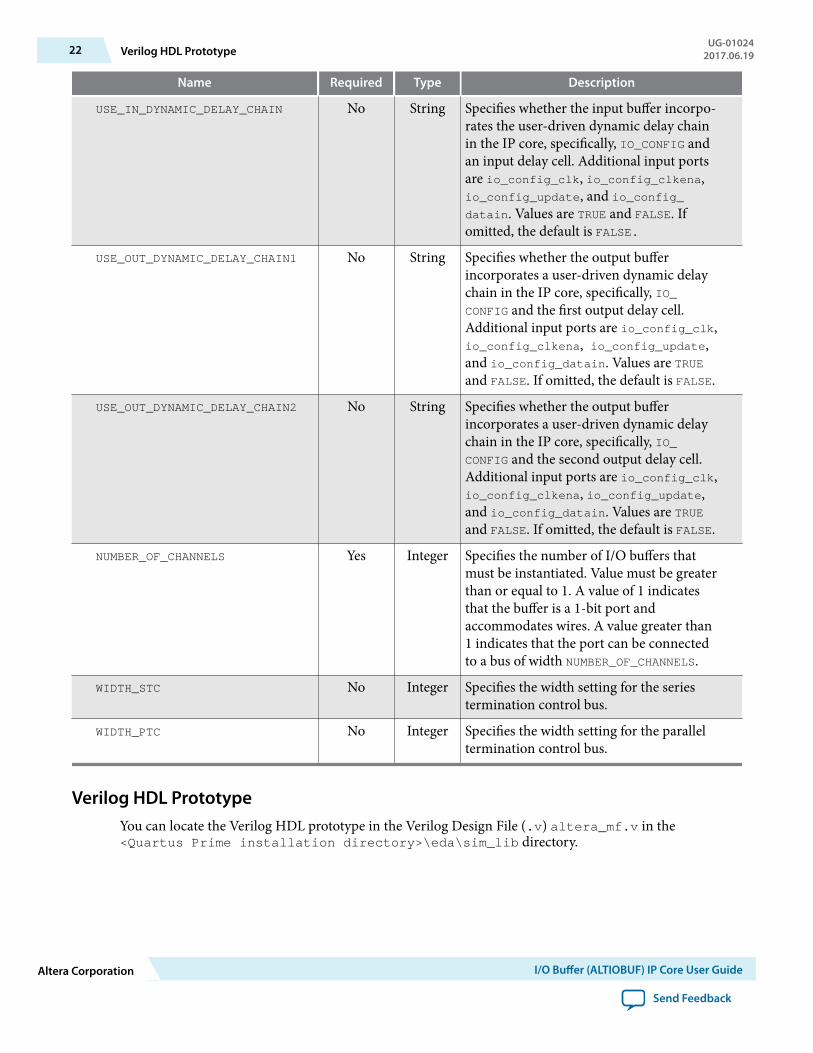
Name Required Type Description
ENABLE_BUS_HOLD No String Specifies whether the bus hold circuitry isenabled. Values are TRUE and FALSE. Whenset to TRUE, bus hold circuitry is enabledand the previous value, instead of highimpedance, is assigned to the output portwhen there is no valid input. If omitted, thedefault is FALSE.
Currently, ENABLE_BUS_HOLD and USE_DIFFERENTIAL_MODE cannot be usedsimultaneously.
USE_DIFFERENTIAL_MODE No String Specifies whether the input buffer isdifferential. Values are TRUE and FALSE.When set to TRUE, the output is thedifference between the datain and datain_b ports. If omitted, the default is FALSE.
Currently, ENABLE_BUS_HOLD and USE_DIFFERENTIAL_MODE cannot be usedsimultaneously.
USE_IN_DYNAMIC_DELAY_CHAIN No String Specifies whether the input buffer incorpo‐rates the user-driven dynamic delay chain inthe IP core, specifically, IO_CONFIG and aninput delay cell. Values are TRUE and FALSE.If omitted, the default is FALSE.
NUMBER_OF_CHANNELS Yes Integer Specifies the number of I/O buffers thatmust be instantiated. Value must be greaterthan or equal to 1. A value of 1 indicatesthat the buffer is a 1-bit port and accommo‐dates wires; a value greater than 1 indicatesthat the port can be connected to a bus ofwidth NUMBER_OF_CHANNELS.
USE_DYNAMIC_TERMINATION_
CONTROL
No String Specifies dynamic termination control.Values are True and False. If omitted, thedefault is False.
ALTIOBUF Signals and Parameters: As Output Buffer
Table 8: ALTIOBUF (As Output Buffer) Input Ports
This table lists the input ports for the ALTIOBUF IP core (as output buffer).
UG-010242017.06.19 ALTIOBUF Signals and Parameters: As Output Buffer 13
I/O Buffer (ALTIOBUF) IP Core User Guide Altera Corporation
Send Feedback
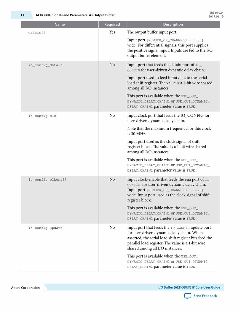
Name Required Description
datain[] Yes The output buffer input port.
Input port [NUMBER_OF_CHANNELS - 1..0]wide. For differential signals, this port suppliesthe positive signal input. Inputs are fed to the I/Ooutput buffer element.
io_config_datain No Input port that feeds the datain port of IO_CONFIG for user-driven dynamic delay chain.
Input port used to feed input data to the serialload shift register. The value is a 1-bit wire sharedamong all I/O instances.
This port is available when the USE_OUT_DYNAMIC_DELAY_CHAIN1 or USE_OUT_DYNAMIC_DELAY_CHAIN2 parameter value is TRUE.
io_config_clk No Input clock port that feeds the IO_CONFIG foruser-driven dynamic delay chain.
Note that the maximum frequency for this clockis 30 MHz.
Input port used as the clock signal of shiftregister block. The value is a 1-bit wire sharedamong all I/O instances.
This port is available when the USE_OUT_DYNAMIC_DELAY_CHAIN1 or USE_OUT_DYNAMIC_DELAY_CHAIN2 parameter value is TRUE.
io_config_clkena[] No Input clock-enable that feeds the ena port of IO_CONFIG for user-driven dynamic delay chain.Input port [NUMBER_OF_CHANNELS - 1..0]wide. Input port used as the clock signal of shiftregister block.
This port is available when the USE_OUT_DYNAMIC_DELAY_CHAIN1 or USE_OUT_DYNAMIC_DELAY_CHAIN2 parameter value is TRUE.
io_config_update No Input port that feeds the IO_CONFIG update portfor user-driven dynamic delay chain. Whenasserted, the serial load shift register bits feed theparallel load register. The value is a 1-bit wireshared among all I/O instances.
This port is available when the USE_OUT_DYNAMIC_DELAY_CHAIN1 or USE_OUT_DYNAMIC_DELAY_CHAIN2 parameter value is TRUE.
14 ALTIOBUF Signals and Parameters: As Output BufferUG-01024
2017.06.19
Altera Corporation I/O Buffer (ALTIOBUF) IP Core User Guide
Send Feedback
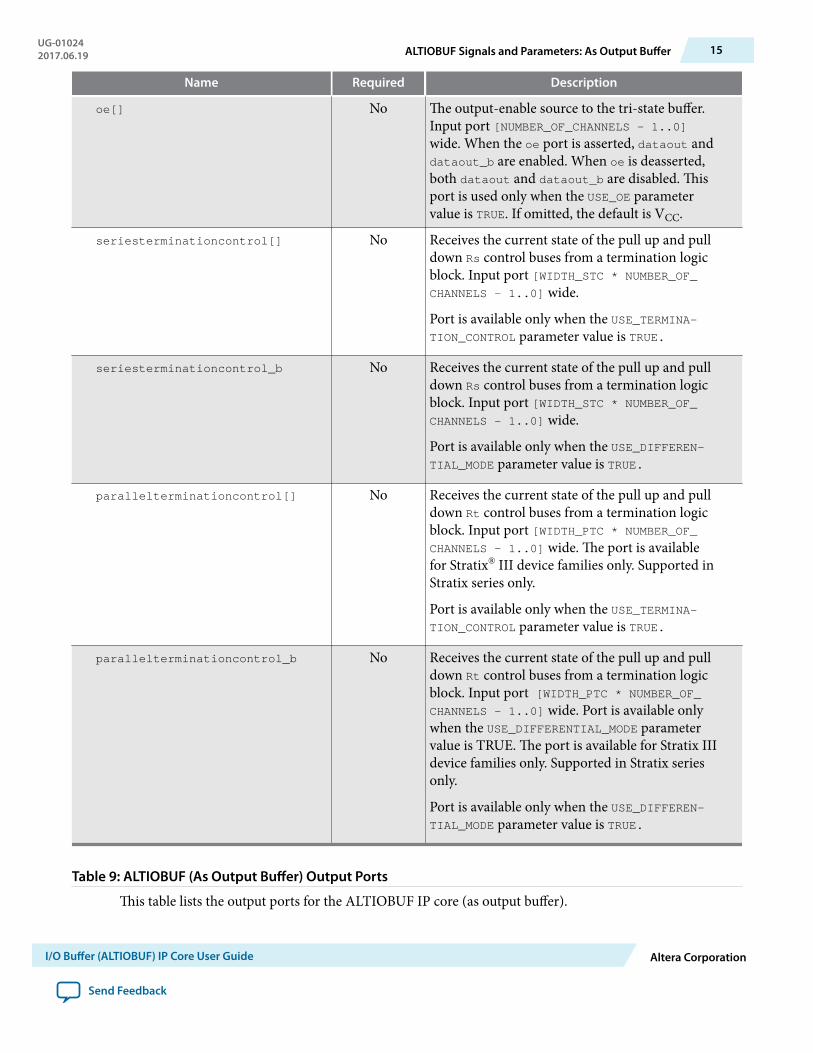
Name Required Description
oe[] No The output-enable source to the tri-state buffer.Input port [NUMBER_OF_CHANNELS - 1..0]wide. When the oe port is asserted, dataout anddataout_b are enabled. When oe is deasserted,both dataout and dataout_b are disabled. Thisport is used only when the USE_OE parametervalue is TRUE. If omitted, the default is VCC.
seriesterminationcontrol[] No Receives the current state of the pull up and pulldown Rs control buses from a termination logicblock. Input port [WIDTH_STC * NUMBER_OF_CHANNELS - 1..0] wide.
Port is available only when the USE_TERMINA-TION_CONTROL parameter value is TRUE.
seriesterminationcontrol_b No Receives the current state of the pull up and pulldown Rs control buses from a termination logicblock. Input port [WIDTH_STC * NUMBER_OF_CHANNELS - 1..0] wide.
Port is available only when the USE_DIFFEREN-TIAL_MODE parameter value is TRUE.
parallelterminationcontrol[] No Receives the current state of the pull up and pulldown Rt control buses from a termination logicblock. Input port [WIDTH_PTC * NUMBER_OF_CHANNELS - 1..0] wide. The port is availablefor Stratix® III device families only. Supported inStratix series only.
Port is available only when the USE_TERMINA-TION_CONTROL parameter value is TRUE.
parallelterminationcontrol_b No Receives the current state of the pull up and pulldown Rt control buses from a termination logicblock. Input port [WIDTH_PTC * NUMBER_OF_CHANNELS - 1..0] wide. Port is available onlywhen the USE_DIFFERENTIAL_MODE parametervalue is TRUE. The port is available for Stratix IIIdevice families only. Supported in Stratix seriesonly.
Port is available only when the USE_DIFFEREN-TIAL_MODE parameter value is TRUE.
Table 9: ALTIOBUF (As Output Buffer) Output Ports
This table lists the output ports for the ALTIOBUF IP core (as output buffer).
UG-010242017.06.19 ALTIOBUF Signals and Parameters: As Output Buffer 15
I/O Buffer (ALTIOBUF) IP Core User Guide Altera Corporation
Send Feedback
Name Required Description
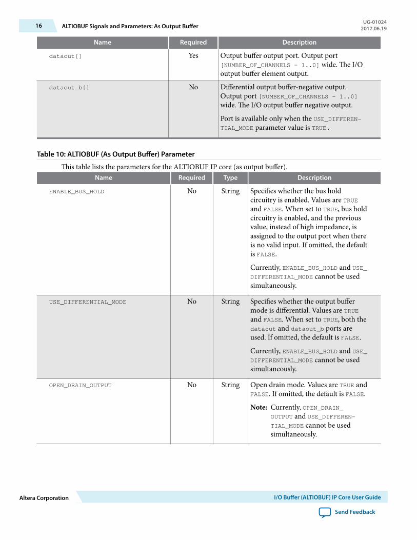
dataout[] Yes Output buffer output port. Output port[NUMBER_OF_CHANNELS - 1..0] wide. The I/Ooutput buffer element output.
dataout_b[] No Differential output buffer-negative output.Output port [NUMBER_OF_CHANNELS - 1..0]wide. The I/O output buffer negative output.
Port is available only when the USE_DIFFEREN-TIAL_MODE parameter value is TRUE.
Table 10: ALTIOBUF (As Output Buffer) Parameter
This table lists the parameters for the ALTIOBUF IP core (as output buffer).Name Required Type Description
ENABLE_BUS_HOLD No String Specifies whether the bus holdcircuitry is enabled. Values are TRUEand FALSE. When set to TRUE, bus holdcircuitry is enabled, and the previousvalue, instead of high impedance, isassigned to the output port when thereis no valid input. If omitted, the defaultis FALSE.
Currently, ENABLE_BUS_HOLD and USE_DIFFERENTIAL_MODE cannot be usedsimultaneously.
USE_DIFFERENTIAL_MODE No String Specifies whether the output buffermode is differential. Values are TRUEand FALSE. When set to TRUE, both thedataout and dataout_b ports areused. If omitted, the default is FALSE.
Currently, ENABLE_BUS_HOLD and USE_DIFFERENTIAL_MODE cannot be usedsimultaneously.
OPEN_DRAIN_OUTPUT No String Open drain mode. Values are TRUE andFALSE. If omitted, the default is FALSE.
Note: Currently, OPEN_DRAIN_OUTPUT and USE_DIFFEREN-TIAL_MODE cannot be usedsimultaneously.
16 ALTIOBUF Signals and Parameters: As Output BufferUG-01024
2017.06.19
Altera Corporation I/O Buffer (ALTIOBUF) IP Core User Guide
Send Feedback
Name Required Type Description
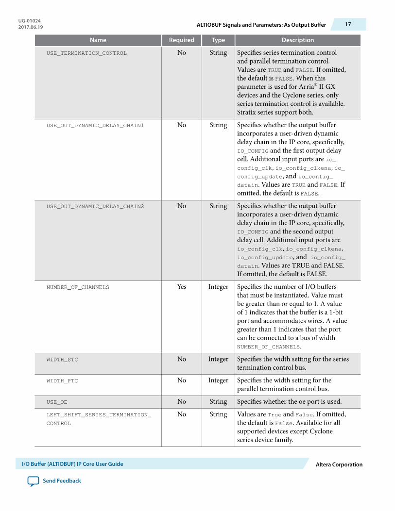
USE_TERMINATION_CONTROL No String Specifies series termination controland parallel termination control.Values are TRUE and FALSE. If omitted,the default is FALSE. When thisparameter is used for Arria® II GXdevices and the Cyclone series, onlyseries termination control is available.Stratix series support both.
USE_OUT_DYNAMIC_DELAY_CHAIN1 No String Specifies whether the output bufferincorporates a user-driven dynamicdelay chain in the IP core, specifically,IO_CONFIG and the first output delaycell. Additional input ports are io_config_clk, io_config_clkena, io_config_update, and io_config_datain. Values are TRUE and FALSE. Ifomitted, the default is FALSE.
USE_OUT_DYNAMIC_DELAY_CHAIN2 No String Specifies whether the output bufferincorporates a user-driven dynamicdelay chain in the IP core, specifically,IO_CONFIG and the second outputdelay cell. Additional input ports areio_config_clk, io_config_clkena,io_config_update, and io_config_datain. Values are TRUE and FALSE.If omitted, the default is FALSE.
NUMBER_OF_CHANNELS Yes Integer Specifies the number of I/O buffersthat must be instantiated. Value mustbe greater than or equal to 1. A valueof 1 indicates that the buffer is a 1-bitport and accommodates wires. A valuegreater than 1 indicates that the portcan be connected to a bus of widthNUMBER_OF_CHANNELS.
WIDTH_STC No Integer Specifies the width setting for the seriestermination control bus.
WIDTH_PTC No Integer Specifies the width setting for theparallel termination control bus.
USE_OE No String Specifies whether the oe port is used.
LEFT_SHIFT_SERIES_TERMINATION_
CONTROL
No String Values are True and False. If omitted,the default is False. Available for allsupported devices except Cycloneseries device family.
UG-010242017.06.19 ALTIOBUF Signals and Parameters: As Output Buffer 17
I/O Buffer (ALTIOBUF) IP Core User Guide Altera Corporation
Send Feedback
Name Required Type Description
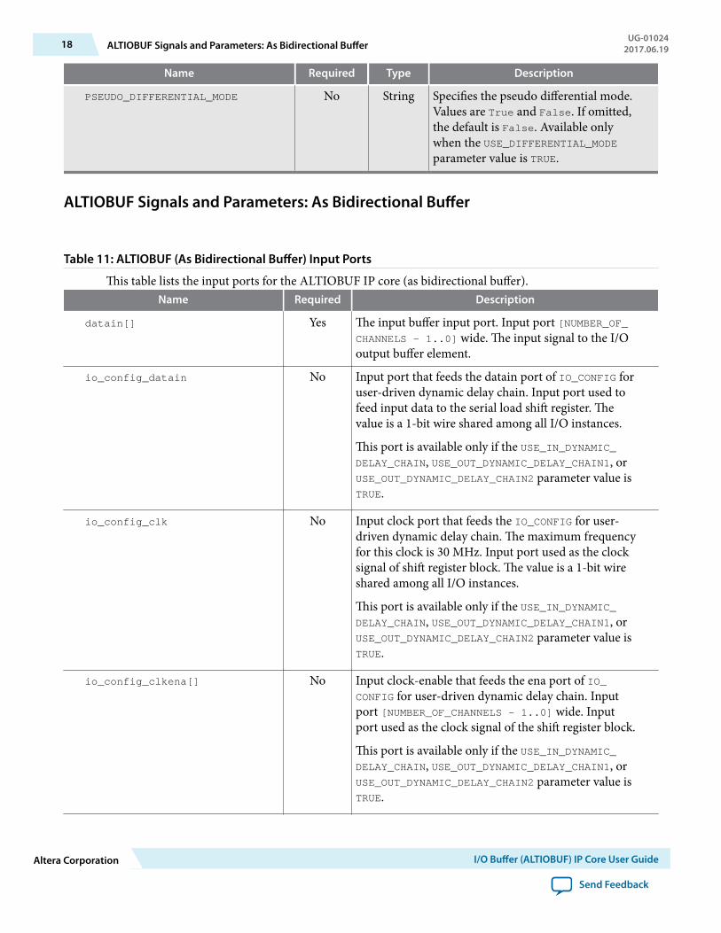
PSEUDO_DIFFERENTIAL_MODE No String Specifies the pseudo differential mode.Values are True and False. If omitted,the default is False. Available onlywhen the USE_DIFFERENTIAL_MODEparameter value is TRUE.
ALTIOBUF Signals and Parameters: As Bidirectional Buffer
Table 11: ALTIOBUF (As Bidirectional Buffer) Input Ports
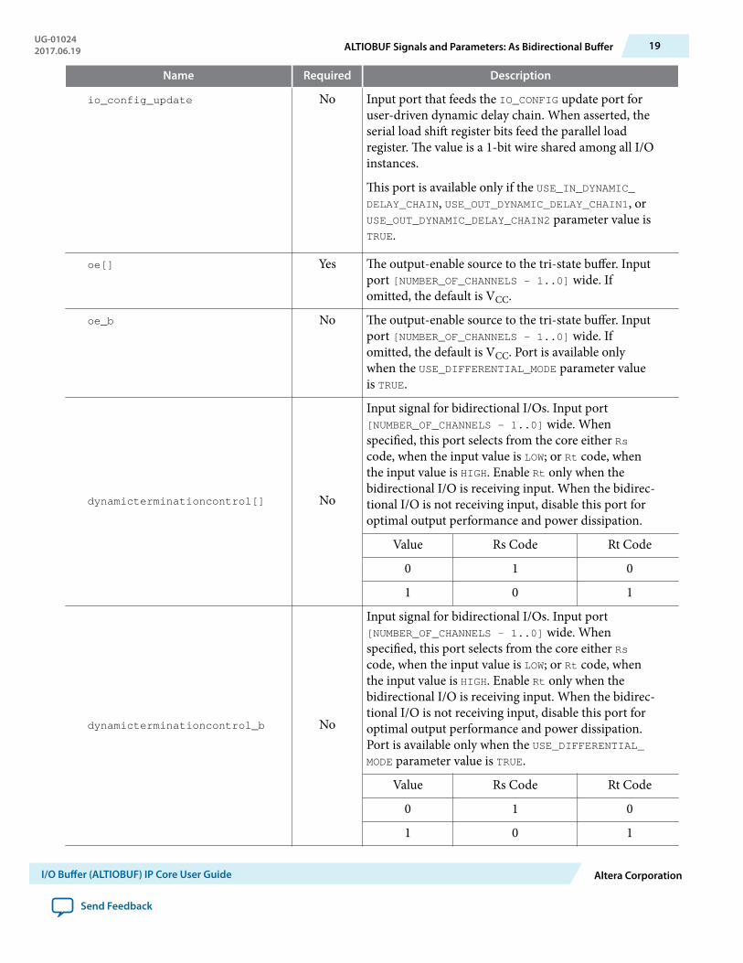
This table lists the input ports for the ALTIOBUF IP core (as bidirectional buffer).Name Required Description
datain[] Yes The input buffer input port. Input port [NUMBER_OF_CHANNELS - 1..0] wide. The input signal to the I/Ooutput buffer element.
io_config_datain No Input port that feeds the datain port of IO_CONFIG foruser-driven dynamic delay chain. Input port used tofeed input data to the serial load shift register. Thevalue is a 1-bit wire shared among all I/O instances.
This port is available only if the USE_IN_DYNAMIC_DELAY_CHAIN, USE_OUT_DYNAMIC_DELAY_CHAIN1, orUSE_OUT_DYNAMIC_DELAY_CHAIN2 parameter value isTRUE.
io_config_clk No Input clock port that feeds the IO_CONFIG for user-driven dynamic delay chain. The maximum frequencyfor this clock is 30 MHz. Input port used as the clocksignal of shift register block. The value is a 1-bit wireshared among all I/O instances.
This port is available only if the USE_IN_DYNAMIC_DELAY_CHAIN, USE_OUT_DYNAMIC_DELAY_CHAIN1, orUSE_OUT_DYNAMIC_DELAY_CHAIN2 parameter value isTRUE.
io_config_clkena[] No Input clock-enable that feeds the ena port of IO_CONFIG for user-driven dynamic delay chain. Inputport [NUMBER_OF_CHANNELS - 1..0] wide. Inputport used as the clock signal of the shift register block.
This port is available only if the USE_IN_DYNAMIC_DELAY_CHAIN, USE_OUT_DYNAMIC_DELAY_CHAIN1, orUSE_OUT_DYNAMIC_DELAY_CHAIN2 parameter value isTRUE.
18 ALTIOBUF Signals and Parameters: As Bidirectional BufferUG-01024
2017.06.19
Altera Corporation I/O Buffer (ALTIOBUF) IP Core User Guide
Send Feedback
Name Required Description
io_config_update No Input port that feeds the IO_CONFIG update port foruser-driven dynamic delay chain. When asserted, theserial load shift register bits feed the parallel loadregister. The value is a 1-bit wire shared among all I/Oinstances.
This port is available only if the USE_IN_DYNAMIC_DELAY_CHAIN, USE_OUT_DYNAMIC_DELAY_CHAIN1, orUSE_OUT_DYNAMIC_DELAY_CHAIN2 parameter value isTRUE.
oe[] Yes The output-enable source to the tri-state buffer. Inputport [NUMBER_OF_CHANNELS - 1..0] wide. Ifomitted, the default is VCC.
oe_b No The output-enable source to the tri-state buffer. Inputport [NUMBER_OF_CHANNELS - 1..0] wide. Ifomitted, the default is VCC. Port is available onlywhen the USE_DIFFERENTIAL_MODE parameter valueis TRUE.
dynamicterminationcontrol[] No
Input signal for bidirectional I/Os. Input port[NUMBER_OF_CHANNELS - 1..0] wide. Whenspecified, this port selects from the core either Rscode, when the input value is LOW; or Rt code, whenthe input value is HIGH. Enable Rt only when thebidirectional I/O is receiving input. When the bidirec‐tional I/O is not receiving input, disable this port foroptimal output performance and power dissipation.
Value Rs Code Rt Code
0 1 0
1 0 1
dynamicterminationcontrol_b No
Input signal for bidirectional I/Os. Input port[NUMBER_OF_CHANNELS - 1..0] wide. Whenspecified, this port selects from the core either Rscode, when the input value is LOW; or Rt code, whenthe input value is HIGH. Enable Rt only when thebidirectional I/O is receiving input. When the bidirec‐tional I/O is not receiving input, disable this port foroptimal output performance and power dissipation.Port is available only when the USE_DIFFERENTIAL_MODE parameter value is TRUE.
Value Rs Code Rt Code
0 1 0
1 0 1
UG-010242017.06.19 ALTIOBUF Signals and Parameters: As Bidirectional Buffer 19
I/O Buffer (ALTIOBUF) IP Core User Guide Altera Corporation
Send Feedback
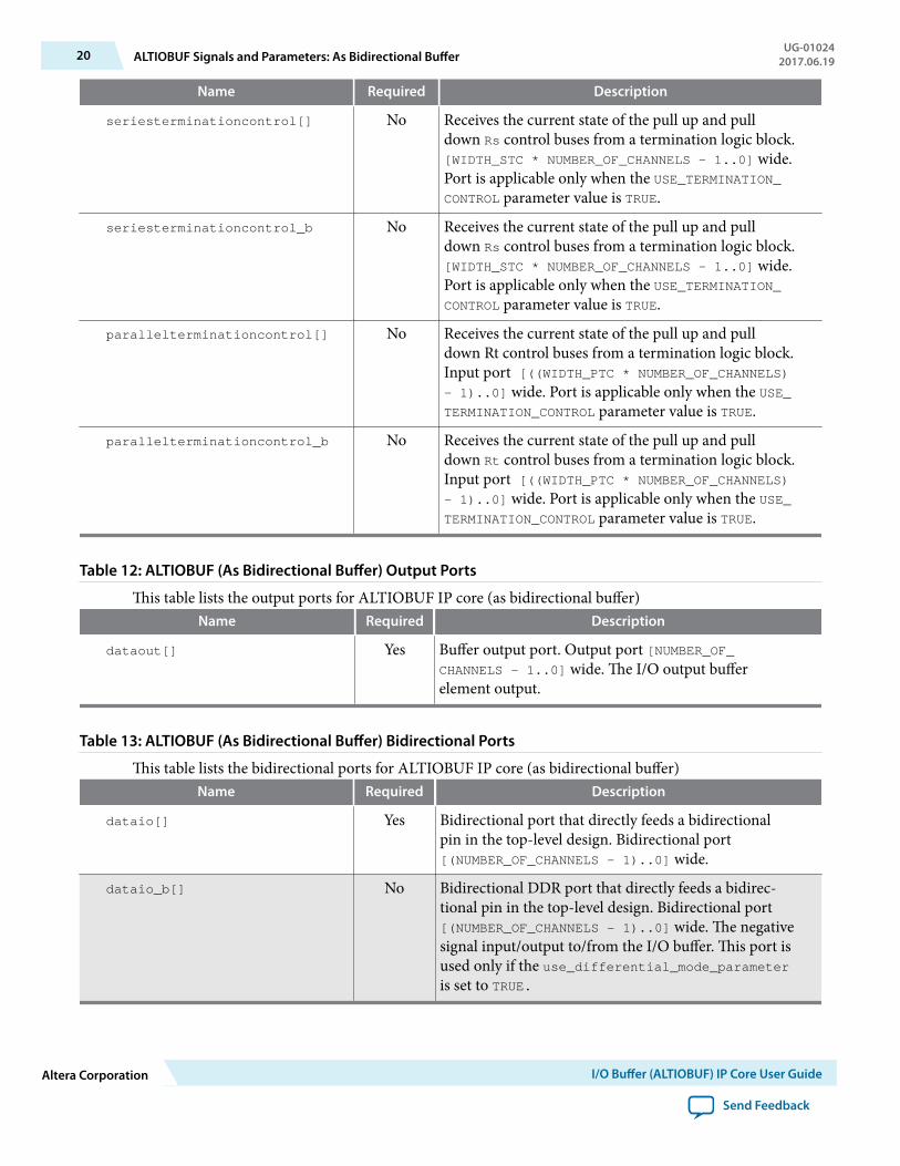
Name Required Description
seriesterminationcontrol[] No Receives the current state of the pull up and pulldown Rs control buses from a termination logic block.[WIDTH_STC * NUMBER_OF_CHANNELS - 1..0] wide.Port is applicable only when the USE_TERMINATION_CONTROL parameter value is TRUE.
seriesterminationcontrol_b No Receives the current state of the pull up and pulldown Rs control buses from a termination logic block.[WIDTH_STC * NUMBER_OF_CHANNELS - 1..0] wide.Port is applicable only when the USE_TERMINATION_CONTROL parameter value is TRUE.
parallelterminationcontrol[] No Receives the current state of the pull up and pulldown Rt control buses from a termination logic block.Input port [((WIDTH_PTC * NUMBER_OF_CHANNELS)- 1)..0] wide. Port is applicable only when the USE_TERMINATION_CONTROL parameter value is TRUE.
parallelterminationcontrol_b No Receives the current state of the pull up and pulldown Rt control buses from a termination logic block.Input port [((WIDTH_PTC * NUMBER_OF_CHANNELS)- 1)..0] wide. Port is applicable only when the USE_TERMINATION_CONTROL parameter value is TRUE.
Table 12: ALTIOBUF (As Bidirectional Buffer) Output Ports
This table lists the output ports for ALTIOBUF IP core (as bidirectional buffer)Name Required Description
dataout[] Yes Buffer output port. Output port [NUMBER_OF_CHANNELS - 1..0] wide. The I/O output bufferelement output.
Table 13: ALTIOBUF (As Bidirectional Buffer) Bidirectional Ports
This table lists the bidirectional ports for ALTIOBUF IP core (as bidirectional buffer)Name Required Description
dataio[] Yes Bidirectional port that directly feeds a bidirectionalpin in the top-level design. Bidirectional port[(NUMBER_OF_CHANNELS - 1)..0] wide.
dataio_b[] No Bidirectional DDR port that directly feeds a bidirec‐tional pin in the top-level design. Bidirectional port[(NUMBER_OF_CHANNELS - 1)..0] wide. The negativesignal input/output to/from the I/O buffer. This port isused only if the use_differential_mode_parameteris set to TRUE.
20 ALTIOBUF Signals and Parameters: As Bidirectional BufferUG-01024
2017.06.19
Altera Corporation I/O Buffer (ALTIOBUF) IP Core User Guide
Send Feedback
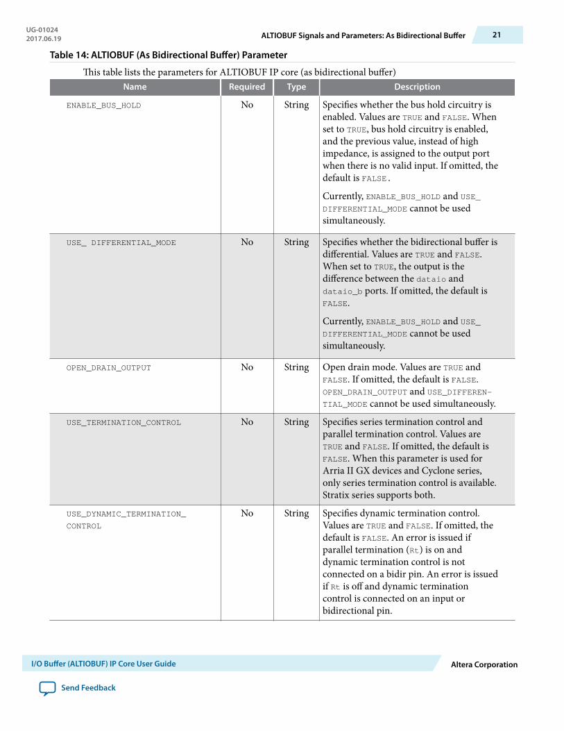
Table 14: ALTIOBUF (As Bidirectional Buffer) Parameter
This table lists the parameters for ALTIOBUF IP core (as bidirectional buffer)Name Required Type Description
ENABLE_BUS_HOLD No String Specifies whether the bus hold circuitry isenabled. Values are TRUE and FALSE. Whenset to TRUE, bus hold circuitry is enabled,and the previous value, instead of highimpedance, is assigned to the output portwhen there is no valid input. If omitted, thedefault is FALSE.
Currently, ENABLE_BUS_HOLD and USE_DIFFERENTIAL_MODE cannot be usedsimultaneously.
USE_ DIFFERENTIAL_MODE No String Specifies whether the bidirectional buffer isdifferential. Values are TRUE and FALSE.When set to TRUE, the output is thedifference between the dataio anddataio_b ports. If omitted, the default isFALSE.
Currently, ENABLE_BUS_HOLD and USE_DIFFERENTIAL_MODE cannot be usedsimultaneously.
OPEN_DRAIN_OUTPUT No String Open drain mode. Values are TRUE andFALSE. If omitted, the default is FALSE.OPEN_DRAIN_OUTPUT and USE_DIFFEREN-TIAL_MODE cannot be used simultaneously.
USE_TERMINATION_CONTROL No String Specifies series termination control andparallel termination control. Values areTRUE and FALSE. If omitted, the default isFALSE. When this parameter is used forArria II GX devices and Cyclone series,only series termination control is available.Stratix series supports both.
USE_DYNAMIC_TERMINATION_
CONTROL
No String Specifies dynamic termination control.Values are TRUE and FALSE. If omitted, thedefault is FALSE. An error is issued ifparallel termination (Rt) is on anddynamic termination control is notconnected on a bidir pin. An error is issuedif Rt is off and dynamic terminationcontrol is connected on an input orbidirectional pin.
UG-010242017.06.19 ALTIOBUF Signals and Parameters: As Bidirectional Buffer 21
I/O Buffer (ALTIOBUF) IP Core User Guide Altera Corporation
Send Feedback
Name Required Type Description
USE_IN_DYNAMIC_DELAY_CHAIN No String Specifies whether the input buffer incorpo‐rates the user-driven dynamic delay chainin the IP core, specifically, IO_CONFIG andan input delay cell. Additional input portsare io_config_clk, io_config_clkena,io_config_update, and io_config_datain. Values are TRUE and FALSE. Ifomitted, the default is FALSE.
USE_OUT_DYNAMIC_DELAY_CHAIN1 No String Specifies whether the output bufferincorporates a user-driven dynamic delaychain in the IP core, specifically, IO_CONFIG and the first output delay cell.Additional input ports are io_config_clk,io_config_clkena, io_config_update,and io_config_datain. Values are TRUEand FALSE. If omitted, the default is FALSE.
USE_OUT_DYNAMIC_DELAY_CHAIN2 No String Specifies whether the output bufferincorporates a user-driven dynamic delaychain in the IP core, specifically, IO_CONFIG and the second output delay cell.Additional input ports are io_config_clk,io_config_clkena, io_config_update,and io_config_datain. Values are TRUEand FALSE. If omitted, the default is FALSE.
NUMBER_OF_CHANNELS Yes Integer Specifies the number of I/O buffers thatmust be instantiated. Value must be greaterthan or equal to 1. A value of 1 indicatesthat the buffer is a 1-bit port andaccommodates wires. A value greater than1 indicates that the port can be connectedto a bus of width NUMBER_OF_CHANNELS.
WIDTH_STC No Integer Specifies the width setting for the seriestermination control bus.
WIDTH_PTC No Integer Specifies the width setting for the paralleltermination control bus.
Verilog HDL PrototypeYou can locate the Verilog HDL prototype in the Verilog Design File (.v) altera_mf.v in the<Quartus Prime installation directory>\eda\sim_lib directory.
22 Verilog HDL PrototypeUG-01024
2017.06.19
Altera Corporation I/O Buffer (ALTIOBUF) IP Core User Guide
Send Feedback
VHDL Component DeclarationYou can locate VHDL component declaration in the VHDL Design File (.vhd) altera_mf_components.vhd in the <Quartus Prime installation directory>\libraries\vhdl\altera_mf directory.
VHDL LIBRARY-USE DeclarationThe VHDL LIBRARY-USE declaration is not required if you use the VHDL Component Declaration.
LIBRARY altera_mf;USE altera_mf.altera_mf_components.all;
I/O Buffer (ALTIOBUF) IP Core User Guide Archives
If an IP core version is not listed, the user guide for the previous IP core version applies.IP Core Version User Guide
14.1 I/O Buffer (ALTIOBUF) IP Core User Guide
Document Revision HistoryThis table lists the revision history for this user guide.
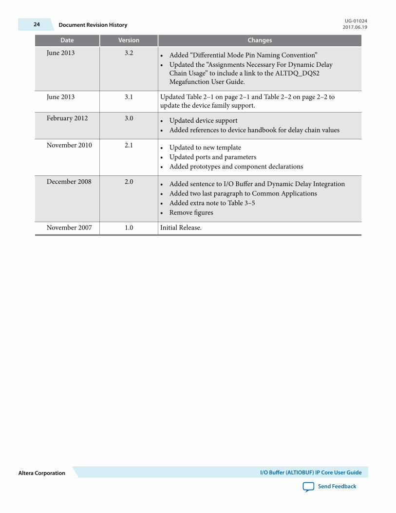
Table 15: Document Revision History
Date Version Changes
June 2017 2017.06.19 • Added support for Cyclone 10 LP devices.• Renamed "Quartus II" to "Quartus Prime".• Removed topics about the installing and licensing IP cores, IP
catalog and parameter editor, customizing and generating IPcores, and upgrading IP cores. These topics are available andupdated in Introduction to Intel FPGA IP Cores.
December 2014 2014.12.15 Template update.
2014.06.30 4.0 • Replaced MegaWizard Plug-In Manager information with IPCatalog.
• Added standard information about upgrading IP cores.• Added standard installation and licensing information.• Removed outdated device support level information. IP core
device support is now available in IP Catalog and parametereditor.
• Removed all references to obsolete SOPC Builder tool.
UG-010242017.06.19 VHDL Component Declaration 23
I/O Buffer (ALTIOBUF) IP Core User Guide Altera Corporation
Send Feedback
Date Version Changes
June 2013 3.2 • Added “Differential Mode Pin Naming Convention”• Updated the “Assignments Necessary For Dynamic Delay
Chain Usage” to include a link to the ALTDQ_DQS2Megafunction User Guide.
June 2013 3.1 Updated Table 2–1 on page 2–1 and Table 2–2 on page 2–2 toupdate the device family support.
February 2012 3.0 • Updated device support• Added references to device handbook for delay chain values
November 2010 2.1 • Updated to new template• Updated ports and parameters• Added prototypes and component declarations
December 2008 2.0 • Added sentence to I/O Buffer and Dynamic Delay Integration• Added two last paragraph to Common Applications• Added extra note to Table 3–5• Remove figures
November 2007 1.0 Initial Release.
24 Document Revision HistoryUG-01024
2017.06.19
Altera Corporation I/O Buffer (ALTIOBUF) IP Core User Guide
Send Feedback