Embed Size (px)
Citation preview
Final Report AOARD 09-4020 Next Generation Proton Beam Writing:
a platform technology for Nanowire Integration
JA van Kan1, AA Bettiol1, T. Osipowicz 2, MBH Breese3, C.H. Sow4 and F Watt5 1Assistant Professor of Physics, NUS,
2Deputy Director of CIBA and Professor of Physics, NUS, 3Deputy head of physics and Assoc. Professor of Physics, NUS
4 Assoc. Professor of Physics, NUS. 5 Director of CIBA and Professor of Physics, NUS.
Centre for Ion Beam Applications (CIBA) Physics department, Faculty of Science, National
University of Singapore (NUS), 2 Science Drive 3 Singapore 117542 Web http://www.ciba.nus.edu.sg
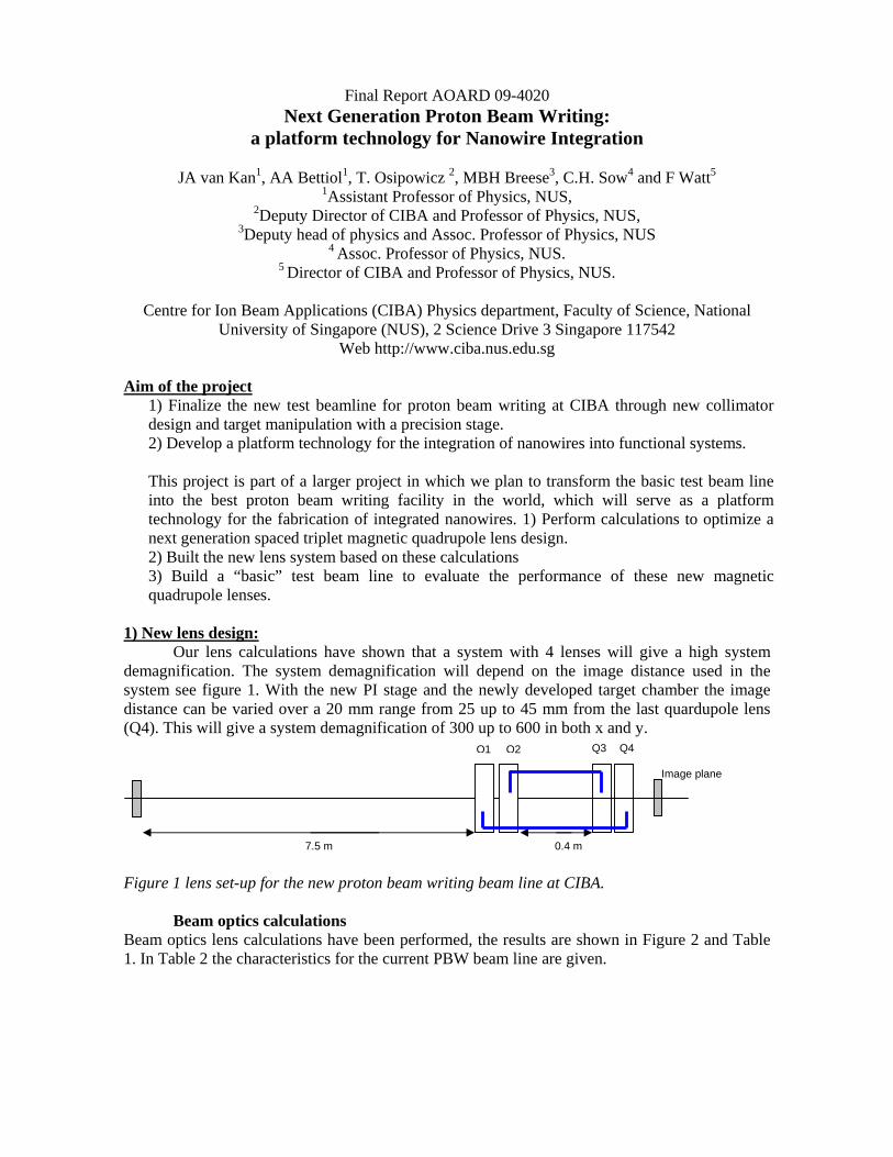
Aim of the project
1) Finalize the new test beamline for proton beam writing at CIBA through new collimator design and target manipulation with a precision stage. 2) Develop a platform technology for the integration of nanowires into functional systems. This project is part of a larger project in which we plan to transform the basic test beam line into the best proton beam writing facility in the world, which will serve as a platform technology for the fabrication of integrated nanowires. 1) Perform calculations to optimize a next generation spaced triplet magnetic quadrupole lens design. 2) Built the new lens system based on these calculations 3) Build a “basic” test beam line to evaluate the performance of these new magnetic quadrupole lenses.
1) New lens design:
Our lens calculations have shown that a system with 4 lenses will give a high system demagnification. The system demagnification will depend on the image distance used in the system see figure 1. With the new PI stage and the newly developed target chamber the image distance can be varied over a 20 mm range from 25 up to 45 mm from the last quardupole lens (Q4). This will give a system demagnification of 300 up to 600 in both x and y.
Figure 1 lens set-up for the new proton beam writing beam line at CIBA.
Beam optics calculations
Beam optics lens calculations have been performed, the results are shown in Figure 2 and Table 1. In Table 2 the characteristics for the current PBW beam line are given.
Q1 Q2 Q3
0.4 m
Image plane
7.5 m
Q4 Proposed system 2
Report Documentation Page Form ApprovedOMB No. 0704-0188
Public reporting burden for the collection of information is estimated to average 1 hour per response, including the time for reviewing instructions, searching existing data sources, gathering andmaintaining the data needed, and completing and reviewing the collection of information. Send comments regarding this burden estimate or any other aspect of this collection of information,including suggestions for reducing this burden, to Washington Headquarters Services, Directorate for Information Operations and Reports, 1215 Jefferson Davis Highway, Suite 1204, ArlingtonVA 22202-4302. Respondents should be aware that notwithstanding any other provision of law, no person shall be subject to a penalty for failing to comply with a collection of information if itdoes not display a currently valid OMB control number.
1. REPORT DATE 01 JUN 2010
2. REPORT TYPE Final
3. DATES COVERED 12-02-2009 to 31-05-2010
4. TITLE AND SUBTITLE Next generation proton beam writing: a platform technology forNannwire integration
5a. CONTRACT NUMBER FA23860914020
5b. GRANT NUMBER
5c. PROGRAM ELEMENT NUMBER
6. AUTHOR(S) Jeroen Van Kan
5d. PROJECT NUMBER
5e. TASK NUMBER
5f. WORK UNIT NUMBER
7. PERFORMING ORGANIZATION NAME(S) AND ADDRESS(ES) Research Center for Nuclear Microscpy, Dept of Physics,National Univ ofSingapore,Lower Kent Ridge Road,Singapore,SN,119260
8. PERFORMING ORGANIZATIONREPORT NUMBER N/A
9. SPONSORING/MONITORING AGENCY NAME(S) AND ADDRESS(ES) Asian Office of Aerospace Research & Development, (AOARD), Unit45002, APO, AP, 96338-5002
10. SPONSOR/MONITOR’S ACRONYM(S) AOARD
11. SPONSOR/MONITOR’S REPORT NUMBER(S) AOARD-094020
12. DISTRIBUTION/AVAILABILITY STATEMENT Approved for public release; distribution unlimited
13. SUPPLEMENTARY NOTES
14. ABSTRACT We designed a new system for proton beam writing. The key characteristics are an improvement of thesystem demagnification of up to 8 and 30 in x and y, respectively compared to commercially availablesystems. The target chamber has show to be working properly and in initial experiments 150 nm beam spotsizes have been obtained. We have shown initial test on proton-beam writing (PBW) for Ni and Aunanowire fabrication, as well as ZnO nanowire fabrication. We have improved the resist development fornano wire template fabrication through optimization of resist which yielded higher resist contrast. A newresist material, TADEP, has been investigated in combination with PBW and has shown details down to110 nm. We have demonstrated the absence of proximity effects in PBW down to 15 nm.
15. SUBJECT TERMS Nan-bio devices, proton micromachining
16. SECURITY CLASSIFICATION OF: 17. LIMITATION OF ABSTRACT Same as
Report (SAR)
18. NUMBEROF PAGES
10
19a. NAME OFRESPONSIBLE PERSON
a. REPORT unclassified
b. ABSTRACT unclassified
c. THIS PAGE unclassified
Standard Form 298 (Rev. 8-98) Prescribed by ANSI Std Z39-18
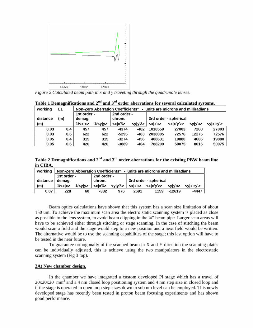
Figure 2 Calculated beam path in x and y traveling through the quadrupole lenses.
Table 1 Demagnifications and 2nd and 3rd order aberrations for several calculated systems. working L1 Non-Zero Aberration Coefficients* - units are microns and milliradians
distance (m) 1st order - demag.
2nd order - chrom. 3rd order - spherical
(m) 1/<x|x> 1/<y|y> <x|x'δ> <y|y'δ> <x|x'3> <x|x'y'2> <y|y'3> <y|x'2y'> 0.03 0.4 457 457 -4374 -482 1018559 27003 7268 270030.03 0.6 622 622 -5295 -483 2038005 72576 12275 725760.05 0.4 315 315 -3274 -456 408631 19880 4606 198800.05 0.6 426 426 -3889 -464 788209 50075 8015 50075
Table 2 Demagnifications and 2nd and 3rd order aberrations for the existing PBW beam line in CIBA. working Non-Zero Abberation Coefficients* - units are microns and milliradians
distance 1st order - demag.
2nd order - chrom. 3rd order - spherical
(m) 1/<x|x> 1/<y|y> <x|x'δ> <y|y'δ> <x|x'3> <x|x'y'2> <y|y'3> <y|x'2y'> 0.07 228 60 -382 976 2691 1159 -12619 -4447
Beam optics calculations have shown that this system has a scan size limitation of about
150 um. To achieve the maximum scan area the electro static scanning system is placed as close as possible to the lens system, to avoid beam clipping in the ¼” beam pipe. Larger scan areas will have to be achieved either through stitching or stage scanning. In the case of stitching the beam would scan a field and the stage would step to a new position and a next field would be written. The alternative would be to use the scanning capabilities of the stage; this last option will have to be tested in the near future.
To guarantee orthogonally of the scanned beam in X and Y direction the scanning plates can be individually adjusted, this is achieve using the two manipulators in the electrostatic scanning system (Fig 3 top). 2A) New chamber design.
In the chamber we have integrated a custom developed PI stage which has a travel of 20x20x20 mm3 and a 4 nm closed loop positioning system and 4 nm step size in closed loop and if the stage is operated in open loop step sizes down to sub nm level can be employed. This newly developed stage has recently been tested in proton beam focusing experiments and has shown good performance.
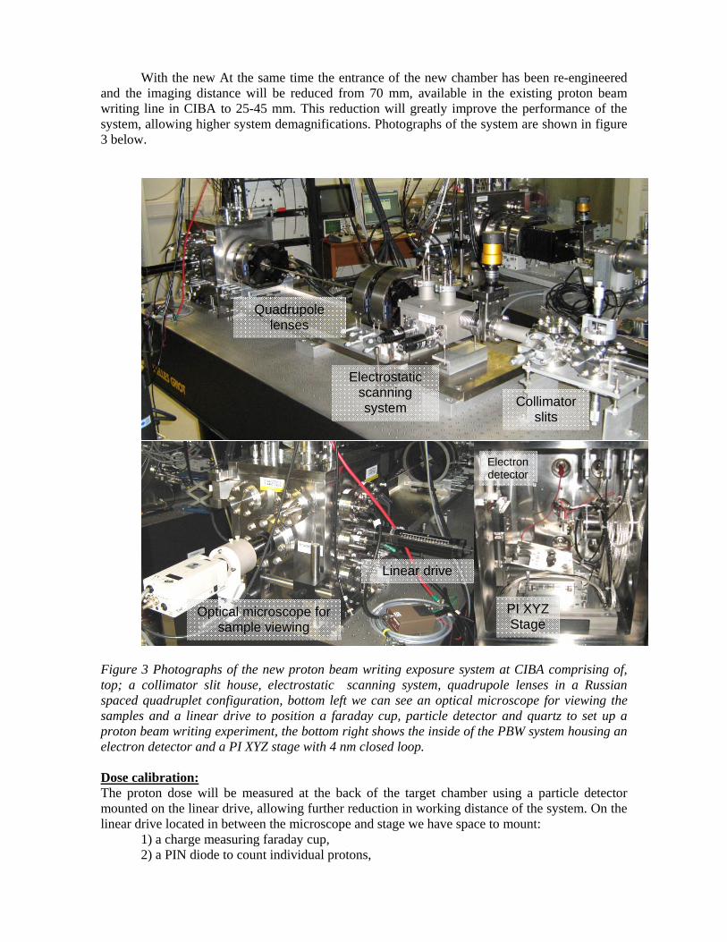
With the new At the same time the entrance of the new chamber has been re-engineered and the imaging distance will be reduced from 70 mm, available in the existing proton beam writing line in CIBA to 25-45 mm. This reduction will greatly improve the performance of the system, allowing higher system demagnifications. Photographs of the system are shown in figure 3 below.
Figure 3 Photographs of the new proton beam writing exposure system at CIBA comprising of, top; a collimator slit house, electrostatic scanning system, quadrupole lenses in a Russian spaced quadruplet configuration, bottom left we can see an optical microscope for viewing the samples and a linear drive to position a faraday cup, particle detector and quartz to set up a proton beam writing experiment, the bottom right shows the inside of the PBW system housing an electron detector and a PI XYZ stage with 4 nm closed loop.
Dose calibration: The proton dose will be measured at the back of the target chamber using a particle detector mounted on the linear drive, allowing further reduction in working distance of the system. On the linear drive located in between the microscope and stage we have space to mount:
1) a charge measuring faraday cup, 2) a PIN diode to count individual protons,
Electrostatic scanning system Collimator
slits
Quadrupole lenses
Optical microscope for sample viewing
Linear drive
PI XYZ Stage
Electron detector
3) A hole to view the sample with the microscope 4) Space for future detectors. A CEM, Channeltron Electron detector for electron microscopy is mounted
just above the stage and is used for easy beam focusing using proton beam induced secondary electrons. In front of the electron detector a metal grid is biased to guide the generated secondary electrons to the electron detector.
2A) New Collimator slit house.
The collimator slit house is located in front of the electrostatic scanning system (see Fig 3 top). The new design can accommodate different slit geometries. This forward scattered beam from different slit geometries will be studied using the PIN diode detector located in the target chamber. In between the collimator slit and the electrostatic scanning system there is a space reserved to test future slit design geometries.
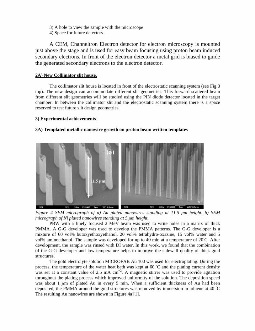
3) Experimental achievements 3A) Templated metallic nanowire growth on proton beam written templates
Figure 4 SEM micrograph of a) Au plated nanowires standing at 11.5 μm height. b) SEM micrograph of Ni plated nanowires standing at 5 μm height.
PBW with a finely focused 2 MeV beam was used to write holes in a matrix of thick PMMA. A G-G developer was used to develop the PMMA patterns. The G-G developer is a mixture of 60 vol% butoxyethoxyethanol, 20 vol% tetrahydro-oxazine, 15 vol% water and 5 vol% aminoethanol. The sample was developed for up to 40 min at a temperature of 20◦C. After development, the sample was rinsed with DI water. In this work, we found that the combination of the G-G developer and low temperature helps to improve the sidewall quality of thick gold structures.
The gold electrolyte solution MICROFAB Au 100 was used for electroplating. During the process, the temperature of the water heat bath was kept at 60 ◦C and the plating current density was set at a constant value of 2.5 mA cm−2. A magnetic stirrer was used to provide agitation throughout the plating process which improved uniformity of the solution. The deposition speed was about 1 μm of plated Au in every 5 min. When a sufficient thickness of Au had been deposited, the PMMA around the gold structures was removed by immersion in toluene at 40 ◦C The resulting Au nanowires are shown in Figure 4a [1].
PBW with a finely focused 2 MeV beam was used to write holes in a matrix of 40 x 40 with a spacing of 1 μm. The array of holes was written in a 10 μm thick PMMA film. After proton beam exposure the sample was developed in a IPA:DI mixture (7:3 by volume) for 10 min followed by a rinse in DI water. The Ni plating was performed in a Technotrans RD50 plating system and the thickness was aimed at half the height of the PMMA layer, resulting in pillars with a height of 5 μm. After plating the resist was removed in toluene at 40◦C for 1 hr. The resulting Ni pillars are shown in Figure 4b [2].
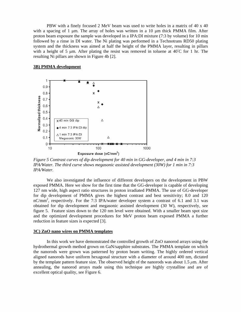
3B) PMMA development
Figure 5 Contrast curves of dip development for 40 min in GG-developer, and 4 min in 7:3 IPA/Water. The third curve shows megasonic assisted development (30W) for 1 min in 7:3 IPA/Water.
We also investigated the influence of different developers on the development in PBW exposed PMMA. Here we show for the first time that the GG-developer is capable of developing 127 nm wide, high aspect ratio structures in proton irradiated PMMA. The use of GG-developer for dip development of PMMA gives the highest contrast and best sensitivity; 8.0 and 120 nC/mm2, respectively. For the 7:3 IPA/water developer system a contrast of 6.1 and 3.1 was obtained for dip development and megasonic assisted development (30 W), respectively, see figure 5. Feature sizes down to the 120 nm level were obtained. With a smaller beam spot size and the optimized development procedures for MeV proton beam exposed PMMA a further reduction in feature sizes is expected [3].
3C) ZnO nano wires on PMMA templates
In this work we have demonstrated the controlled growth of ZnO nanorod arrays using the
hydrothermal growth method grown on GaN/sapphire substrates. The PMMA template on which the nanorods were grown was patterned by proton beam writing. The highly ordered vertical aligned nanorods have uniform hexagonal structure with a diameter of around 400 nm, dictated by the template pattern feature size. The observed height of the nanorods was about 1.5 μm. After annealing, the nanorod arrays made using this technique are highly crystalline and are of excellent optical quality, see Figure 6.
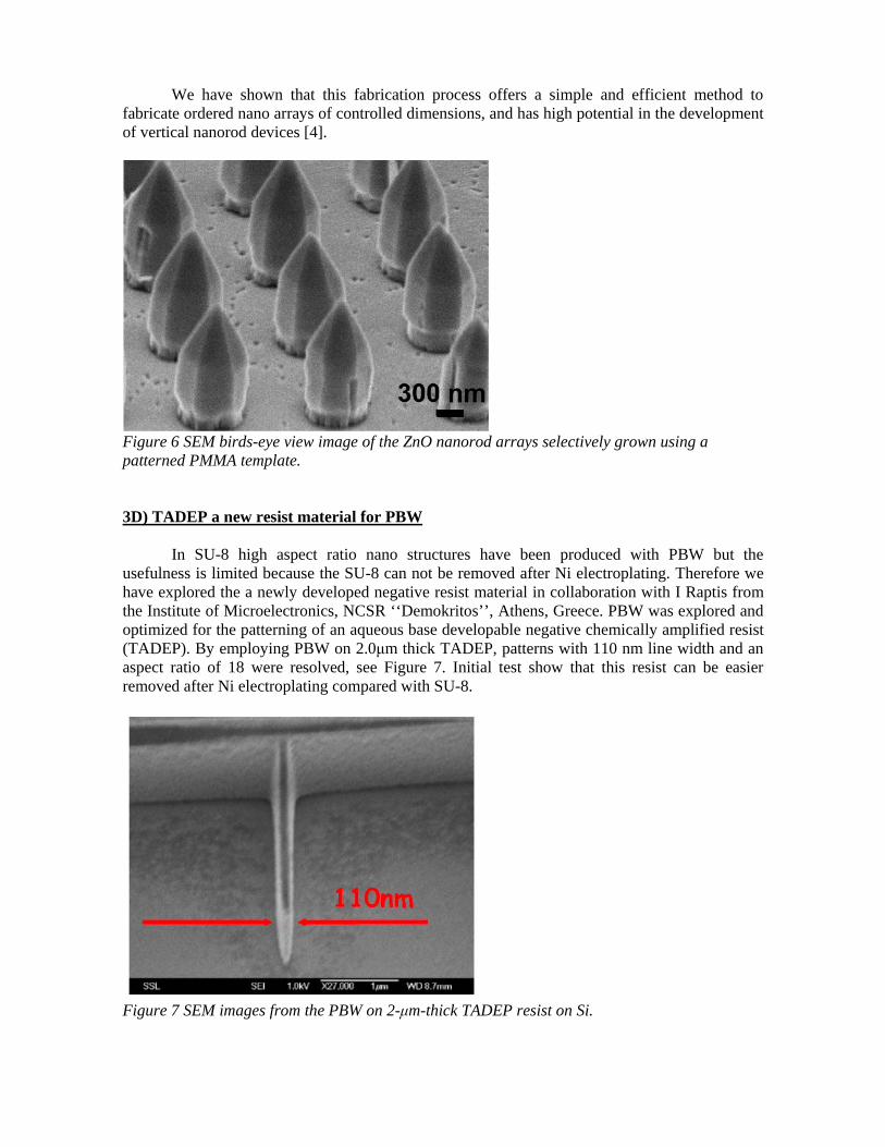
We have shown that this fabrication process offers a simple and efficient method to fabricate ordered nano arrays of controlled dimensions, and has high potential in the development of vertical nanorod devices [4].
Figure 6 SEM birds-eye view image of the ZnO nanorod arrays selectively grown using a patterned PMMA template. 3D) TADEP a new resist material for PBW
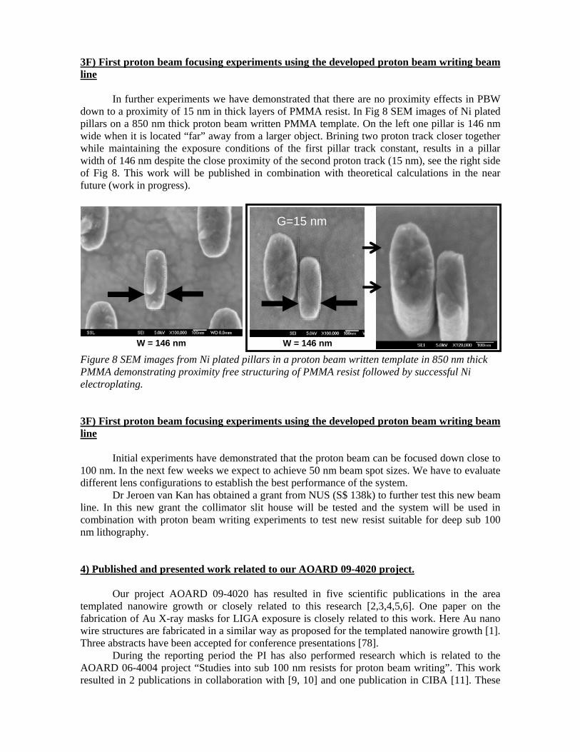
In SU-8 high aspect ratio nano structures have been produced with PBW but the usefulness is limited because the SU-8 can not be removed after Ni electroplating. Therefore we have explored the a newly developed negative resist material in collaboration with I Raptis from the Institute of Microelectronics, NCSR ‘‘Demokritos’’, Athens, Greece. PBW was explored and optimized for the patterning of an aqueous base developable negative chemically amplified resist (TADEP). By employing PBW on 2.0μm thick TADEP, patterns with 110 nm line width and an aspect ratio of 18 were resolved, see Figure 7. Initial test show that this resist can be easier removed after Ni electroplating compared with SU-8.
Figure 7 SEM images from the PBW on 2-μm-thick TADEP resist on Si.
3F) First proton beam focusing experiments using the developed proton beam writing beam line
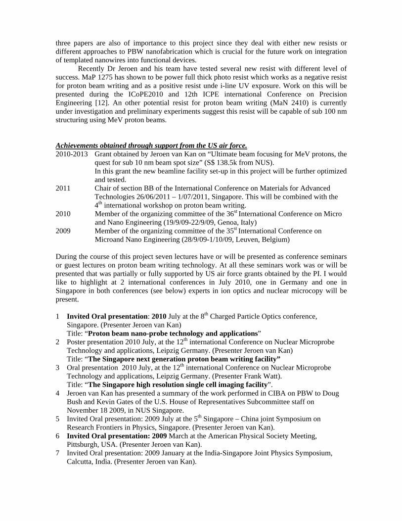
In further experiments we have demonstrated that there are no proximity effects in PBW down to a proximity of 15 nm in thick layers of PMMA resist. In Fig 8 SEM images of Ni plated pillars on a 850 nm thick proton beam written PMMA template. On the left one pillar is 146 nm wide when it is located “far” away from a larger object. Brining two proton track closer together while maintaining the exposure conditions of the first pillar track constant, results in a pillar width of 146 nm despite the close proximity of the second proton track (15 nm), see the right side of Fig 8. This work will be published in combination with theoretical calculations in the near future (work in progress).
Figure 8 SEM images from Ni plated pillars in a proton beam written template in 850 nm thick PMMA demonstrating proximity free structuring of PMMA resist followed by successful Ni electroplating. 3F) First proton beam focusing experiments using the developed proton beam writing beam line
Initial experiments have demonstrated that the proton beam can be focused down close to 100 nm. In the next few weeks we expect to achieve 50 nm beam spot sizes. We have to evaluate different lens configurations to establish the best performance of the system.
Dr Jeroen van Kan has obtained a grant from NUS (S$ 138k) to further test this new beam line. In this new grant the collimator slit house will be tested and the system will be used in combination with proton beam writing experiments to test new resist suitable for deep sub 100 nm lithography.
4) Published and presented work related to our AOARD 09-4020 project.
Our project AOARD 09-4020 has resulted in five scientific publications in the area templated nanowire growth or closely related to this research [2,3,4,5,6]. One paper on the fabrication of Au X-ray masks for LIGA exposure is closely related to this work. Here Au nano wire structures are fabricated in a similar way as proposed for the templated nanowire growth [1]. Three abstracts have been accepted for conference presentations [78].
During the reporting period the PI has also performed research which is related to the AOARD 06-4004 project “Studies into sub 100 nm resists for proton beam writing”. This work resulted in 2 publications in collaboration with [9, 10] and one publication in CIBA [11]. These
W = 146 nm W = 146 nm
G=15 nm
three papers are also of importance to this project since they deal with either new resists or different approaches to PBW nanofabrication which is crucial for the future work on integration of templated nanowires into functional devices.
Recently Dr Jeroen and his team have tested several new resist with different level of success. MaP 1275 has shown to be power full thick photo resist which works as a negative resist for proton beam writing and as a positive resist unde i-line UV exposure. Work on this will be presented during the ICoPE2010 and 12th ICPE international Conference on Precision Engineering [12]. An other potential resist for proton beam writing (MaN 2410) is currently under investigation and preliminary experiments suggest this resist will be capable of sub 100 nm structuring using MeV proton beams. Achievements obtained through support from the US air force. 2010-2013 Grant obtained by Jeroen van Kan on “Ultimate beam focusing for MeV protons, the
quest for sub 10 nm beam spot size” (S$ 138.5k from NUS). In this grant the new beamline facility set-up in this project will be further optimized
and tested. 2011 Chair of section BB of the International Conference on Materials for Advanced
Technologies 26/06/2011 – 1/07/2011, Singapore. This will be combined with the 4th international workshop on proton beam writing.
2010 Member of the organizing committee of the 36st International Conference on Micro and Nano Engineering (19/9/09-22/9/09, Genoa, Italy)
2009 Member of the organizing committee of the 35st International Conference on Microand Nano Engineering (28/9/09-1/10/09, Leuven, Belgium)
During the course of this project seven lectures have or will be presented as conference seminars or guest lectures on proton beam writing technology. At all these seminars work was or will be presented that was partially or fully supported by US air force grants obtained by the PI. I would like to highlight at 2 international conferences in July 2010, one in Germany and one in Singapore in both conferences (see below) experts in ion optics and nuclear microcopy will be present. 1 Invited Oral presentation: 2010 July at the 8th Charged Particle Optics conference,
Singapore. (Presenter Jeroen van Kan) Title: “Proton beam nano-probe technology and applications”
2 Poster presentation 2010 July, at the 12th international Conference on Nuclear Microprobe Technology and applications, Leipzig Germany. (Presenter Jeroen van Kan) Title: “The Singapore next generation proton beam writing facility”
3 Oral presentation 2010 July, at the 12th international Conference on Nuclear Microprobe Technology and applications, Leipzig Germany. (Presenter Frank Watt). Title: “The Singapore high resolution single cell imaging facility”.
4 Jeroen van Kan has presented a summary of the work performed in CIBA on PBW to Doug Bush and Kevin Gates of the U.S. House of Representatives Subcommittee staff on November 18 2009, in NUS Singapore.
5 Invited Oral presentation: 2009 July at the 5th Singapore – China joint Symposium on Research Frontiers in Physics, Singapore. (Presenter Jeroen van Kan).
6 Invited Oral presentation: 2009 March at the American Physical Society Meeting, Pittsburgh, USA. (Presenter Jeroen van Kan).
7 Invited Oral presentation: 2009 January at the India-Singapore Joint Physics Symposium, Calcutta, India. (Presenter Jeroen van Kan).
5) Summary
We have designed a new system for proton beam writing. The key characteristics are an improvement of the system demagnification of up to 8 and 30 in x and y respectively compared to commercially available systems from Oxford Microbeams. The target chamber has show to be working properly and in initial experiments 150 nm beam spot sizes have been obtained.
We have shown initial test on PBW for Ni and Au nanowire fabrication as well as ZnO nanowire fabrication. We have improved the resist development for nano wire template fabrication through optimization of resist which yielded higher resist contrast using the GG developer. A new resist material, TADEP has been investigated in combination with PBW and has shown details down to 110 nm. We have demonstrated the absence of proximity effects in PBW down to 15 nm. The PI has conducted seven talks and posters on Proton Beam Writing in which research is presented that was supported through this grant from the US air force. Assistant proffesor Dr. Jeroen A. Van Kan Centre for Ion Beam Applications (CIBA), The National University of Singapore 2 Science Drive 3, Singapore 117542 Tel: (65) 6516 6978, (65) 6516 2639(lab) Fax: : (65) 67776126 E-mail: [email protected] Web http://www.CIBA.nus.edu.sg
References 1 Proton beam writing and electroplating for the fabrication of high-aspect-ratio Au
microstructures, Weisheng Yue, Yaping Ren, Jeroen Anton van Kan, Sher-Yi Chiam, Linke Jian, Herbert O. Moser, Thomas Osipowicz, Frank Watt, Nuclear Instruments & Methods in Physics Research Section B Volume 267 (2009) 2376-2380
2 Proton beam writing: a platform technology for nanowire production, J. A. van Kan F. Zhang S. Y. Chiam T. Osipowicz A. A. Bettiol F. Watt, Microsystem Technologies, V14, (2008) pp1343-1348.
3 Enhancement of proton beam writing in PMMA through optimization of the development procedure, S. Bolhuis, J.A. van Kan, F. Watt, Nuclear Instruments & Methods in Physics Research Section B. Volume 267 (2009) 2302-2305.
4 Selective Growth of ZnO Nanorod Arrays on a GaN/Sapphire Substrate Using a Proton Beam Written Mask, HL Zhou, PG Shao, SJ Chua, JA van Kan, AA Bettiol, T Osipowicz, KF Ooi, GKL Goh, F Watt, Crystal Growth & Design, 8 (2008) 4445-4448.
5 Proton beam written hydrogen silsesquioxane (HSQ) nanostructures for Nickel electroplating, S. Gorelick, F. Zhang, P.G. Shao, J.A. van Kan, Harry J. Whitlow, F. Watt, Nuclear Instruments & Methods in Physics Research Section B. Volume 267 (2009) 2309-2311.
6 Proton Beam Writing: a Platform Technology for Nano-integration, J.A. van Kan, F. Zhang, A.A. Bettiol and F. Watt Proceedings of SPIE, V6921 (2008) 69210K-1, 69210K-8
7 The Singapore next generation proton beam writing facility, J.A. van Kan, A.B. de Vera, A.A. Bettiol and F. Watt, Abstract presented at the 12th international Conference on Nuclear Microprobe Technology and applications, Leipzig Germany, 2010.
8 The Singapore high resolution single cell imaging facility. F. Watt, Chen Xiao, A. Baysic De Vera, C.C.N. Udalagama, Ren Minqin, J. van Kan and A. Bettiol. Abstract presented at the 12th international Conference on Nuclear Microprobe Technology and applications, Leipzig Germany, 2010.
9 High aspect ratio micro/nano machining with proton beam writing on aqueous developable – easily stripped negative chemically-amplified resists, M. Chatzichristidi, E. Valamontes, P. Argitis, I. Raptis, J.A. van Kan, F. Zhang, F. Watt Microelectronic Engineering 85 (2008) 945–948.
10 Realization and Simulation of High-Aspect-Ratio Micro/Nanostructures by Proton Beam Writing, E. Valamontes, M. Chatzichristidi, N. Tsikrikas, D. Goustouridis, I. Raptis, C. Potiriadis, J.A. van Kan, F. Watt, JJAP, 47 (2008) 8600-8605.
11 Exposure parameters in proton beam writing for hydrogen silsesquioxane, J.A. van Kan, F. Zhang, C. Zhang, A.A. Bettiol, F. Watt, Nuclear Instruments & Methods in Physics Research Section B-Volume 266 (2008) 1676–1679.
12 Nickel injection mould fabrication via proton beam writing and UV lithography, Liu Nan Nan, Shao Peige, Shripad R. Kulkarni, Zhao Jianhong, and Jeroen A van Kan, acceptred for publication (2010).