Embed Size (px)
Citation preview
VISVESVARAYA TECHNOLOGICAL UNIVERSITY
BELAGAVI-590018, KARNATAKA
PROJECT REPORT
ON
“HIGH STEP-UP CONVERTER WITH VOLTAGE MULTIPLIER MODULE
FOR RENEWABLE ENERGY SYSTEM”
Project Report submitted in partial fulfillment of the requirement for the award
of the degree of
Bachelor of Engineering
In
Electronics and Communication Engineering
For the academic year 2019-20
Submitted by
NAME: USN:
ABHILASH V 1CR16EC001
DILIP KUMAR N M 1CR16EC039
GIRISH REDDY Y 1CR16EC043
Under the guidance of
Dr Naveen Kumar G N
Associate. Professor
Department Of Electronics and Communication Engineering
Feb – June 2020
Department Of Electronics and Communication Engineering
CMR INSTITUTE OF TECHNOLOGY
DEPARTMENT OF ELECTRONICS AND COMMUNICATION ENGINEERING
CERTIFICATE
This is to Certify that the dissertation work entitled “High Setup Converter with Voltage
Multiplier Module for Renewable Energy System”, prepared by Abhilash V 1CR16EC001,
Dilip Kumar N M 1CR16EC039,Girish Reddy Y 1CR16EC043 , a bona fide student of CMR
Institute of Technology, Bangalore in partial fulfillment of the requirements for the award of
Bachelor of Engineering in Electronics and Communication Engineering of the Visvesvaraya
Technological University, Belagavi-590018 during the academic year 2019-20.
This is certified that all the corrections and suggestions indicated for Internal Assessment have been
incorporated in the report deposited in the departmental library. The seminar report has been
approved as it satisfies the academic requirements prescribed for the said degree.
---------------------- ----------------------- -----------------------
Signature of Guide Signature of HOD Signature of PRINCIPAL
Dr. Naveen Kumar G N Dr. R Elumalai Dr.Sanjay Jain
Asst. Professor Professor & HOD Principal
Dept. of ECE, CMRIT Dept. of ECE, CMRIT CMRIT, Bangalore
External Viva
Name of Examiners
1.
Signature & date
2
ACKNOWLEDGEMENT
The satisfaction and euphoria that accompany the successful completion of any task would be
incomplete without the mention of people who made it possible, whose consistent guidance and
encouragement crowned our efforts with success.
We consider it as our privilege to express the gratitude to all those who guided in the completion
of the project.
We express my gratitude to Principal, Dr. Sanjay Jain, for having provided us the golden
opportunity to undertake this project work in their esteemed organization.
We sincerely thank Dr. R. Elumalai, HOD, Department of Electronics and Communication
Engineering, CMR Institute of Technology for the immense support given to us.
We express my gratitude to our project guide Dr Naveen Kumar G N, Associate. Professor, for
their support, guidance and suggestions throughout the project work.
Last but not the least, heartful thanks to our parents and friends for their support.
Above all, we thank the Lord Almighty for His grace on us to succeed in this endeavor.
ABHILASH V (1CR16EC001)
DILIP KUMAR N M (1CR16EC039)
GIRISH REDDY Y (1CR16EC043)

ABSTRACT
We proposed a High step – up converter for renewable energy applications through
an adjustable voltage of the multiplier module, the proposed high step up converter
gain without any utilizing larger duty ratio or a high turn ratio. The voltage
multiplier modules are composed of inductors and switch capacitors. Due to the
passive lossless clamped performances, leakage energy will be recycled which will
be having high voltage spike across the main switch and improves efficiency.
Thus, the power switches with the low levels of the voltages stress can be adopted
for loses in the conduction. So for in addition of the isolated topology of the
proposed converter satisfies electrical isolation and safety regulations. Also in our
proposed converter will be having continuous and smooth running input current,
which will be in decreases the conduction losses the lengthens life time of the input
source and constrains conducted in electromagnetic interference problems in solar
panel. Finally a prototype circuit with 40 V input voltage, 380 V output, and 500
W maximum output power is operated to verify its performance according to our
work. The maximum efficiency is 94.99% at 200 W and the full load efficiency is
90.87% at 500W.

CONTENTS
CERTIFICATE i
ACKNOWLEDGEMENT ii
ABSTRACT iii
CHAPTERS PAGE NO
1. Introduction 03
1.1 Common Power Devices 05
1.2 Proposed System 10
1.3 Block Diagram 12
2. Literature Survey 13
3. Components Description 16
3.1 PIC16F877A 17
3.2 MOSFET 35
3.3 Gate Driver Circuit 36
3.4 Rectifier 38
3.5 Filter 41
3.6 Buffer 42
3.7 Inverter 43
3.8 Solar Panel 47
3.9 Voltage Multiplier 56
4. Mat lab Simulation 57
4.1 Simulation Of solar cell 57
4.2 interleaved boost converter with 58
voltage multiplier 58
4.3 Full Circuit 58
5. Result 59
5.1 Conclusion 62
6. References 63
High Step-Up Converter With Voltage Multiplier Module For Renewable Energy System
Dept Of ECE-CMRIT Page 3
CHAPTER 1
INTRODUCTION:
Power Electronics is the art of converting electrical energy from one form to another in
an efficient, clean, compact, and robust manner for convenient utilisation. A passenger lift in a
modern building equipped with a Variable-Voltage-Variable-Speed induction-machine drive
offers a comfortable ride and stops exactly at the floor level. Behind the scene it consumes less
power with reduced stresses on the motor and corruption of the utility mains.
Power Electronics involves the study of
• Power semiconductor devices - their physics, characteristics, drive requirements and their
protection for optimum utilisation of their capacities,
• Power converter topologies involving them,
• Control strategies of the converters,
• Digital, analogue and microelectronics involved,
• Capacitive and magnetic energy storage elements,
• Rotating and static electrical devices,
• Quality of waveforms generated,
• Electro Magnetic and Radio Frequency Interference
Power electronic converters - to modify the form of electrical energy (voltage, current or
frequency).
Power range - from some milli watts (mobile phone) to hundreds of megawatts (HVDC
transmission system). With "classical" electronics, electrical currents and voltage are used to
carry information, whereas with power electronics, they carry power. Thus, the main metric of
power electronics becomes the efficiency.
The first very high power electronic devices were mercury arc valves. In modern systems
the conversion is performed with semiconductor switching devices such as diodes,
thyristors and transistors. In contrast to electronic systems concerned with transmission and
processing of signals and data, in power electronics substantial amounts of electrical energy are
processed.
High Step-Up Converter With Voltage Multiplier Module For Renewable Energy System
Dept Of ECE-CMRIT Page 2
An AC/DC converter (rectifier) is the most typical power electronics device found in
many consumer electronic devices, e.g., television sets, personal computers, battery chargers,
etc. The power range is typically from tens of watts to several hundred watts. In industry the
most common application is the variable speed drive that is used to control an induction motor.
The power range of VSDs start from a few hundred watts and end at tens of megawatts.
The power conversion systems can be classified according to the type of the input and output
power
AC to DC (rectification)
DC to AC (inversion)
DC to DC (chopping)
AC to AC (transformation)
PRINCIPLE
The instantaneous dissipated power of a device P = V.I
Thus, losses of a power device are at a minimum when the voltage across it is zero (the
device is in the On-State) or when no current flows through it (Off-State). Therefore, a power
electronic converter is built around one (or more) device operating in switching mode (either On
or Off).
APPLICATIONS
Power electronic systems are found in virtually every electronic device. For example:
DC/DC converters are used in most mobile devices (mobile phones, PDA etc.) to
maintain the voltage at a fixed value whatever the voltage level of the battery is. These
converters are also used for electronic isolation and power factor correction.
AC/DC converters (rectifiers) are used every time an electronic device is connected to the
mains (computer, television etc.). These may simply change AC to DC or can also
change the voltage level as part of their operation.
High Step-Up Converter With Voltage Multiplier Module For Renewable Energy System
Dept Of ECE-CMRIT Page 3
AC/AC converters are used to change either the voltage level or the frequency
(international power adapters, light dimmer). In power distribution networks AC/AC
converters may be used to exchange power between utility frequency50 Hz and 60 Hz
power grids.
DC/AC converters (inverters) are used primarily in UPS or emergency lighting systems.
When mains power is available, it will charge the DC battery. If the mains fails, an
inverter will be used to produce AC electricity at mains voltage from the DC battery.
COMMON POWER DEVICES
Some common power devices are the power diode, thyristor, power
MOSFET and IGBT(insulated gate bipolar transistor). A power diode or MOSFET
operates on similar principles to its low-power counterpart, but is able to carry a larger
amount of current and typically is able to support a larger reverse-bias voltage in the off-
state.
Structural changes are often made in power devices to accommodate the higher current
density, higher power dissipation and/or higher reverse breakdown voltage. The vast
majority of the discrete (i.e non integrated) power devices are built using a vertical
structure, whereas small-signal devices employ a lateral structure. With the vertical
structure, the current rating of the device is proportional to its area, and the voltage
blocking capability is achieved in the height of the die. With this structure, one of the
connections of the device is located on the bottom of the semiconductor.
Power semiconductor devices
These are semiconductor devices used as switches or rectifiers in power
electronic circuits(switch mode power supplies for example). They are also called power
devices or when used in integrated circuits, called power ICs.
Most power semiconductor devices are only used in commutation mode (i.e they are either
on or off), and are therefore optimized for this. Most of them should not be used in linear
operation.
High Step-Up Converter With Voltage Multiplier Module For Renewable Energy System
Dept Of ECE-CMRIT Page 4
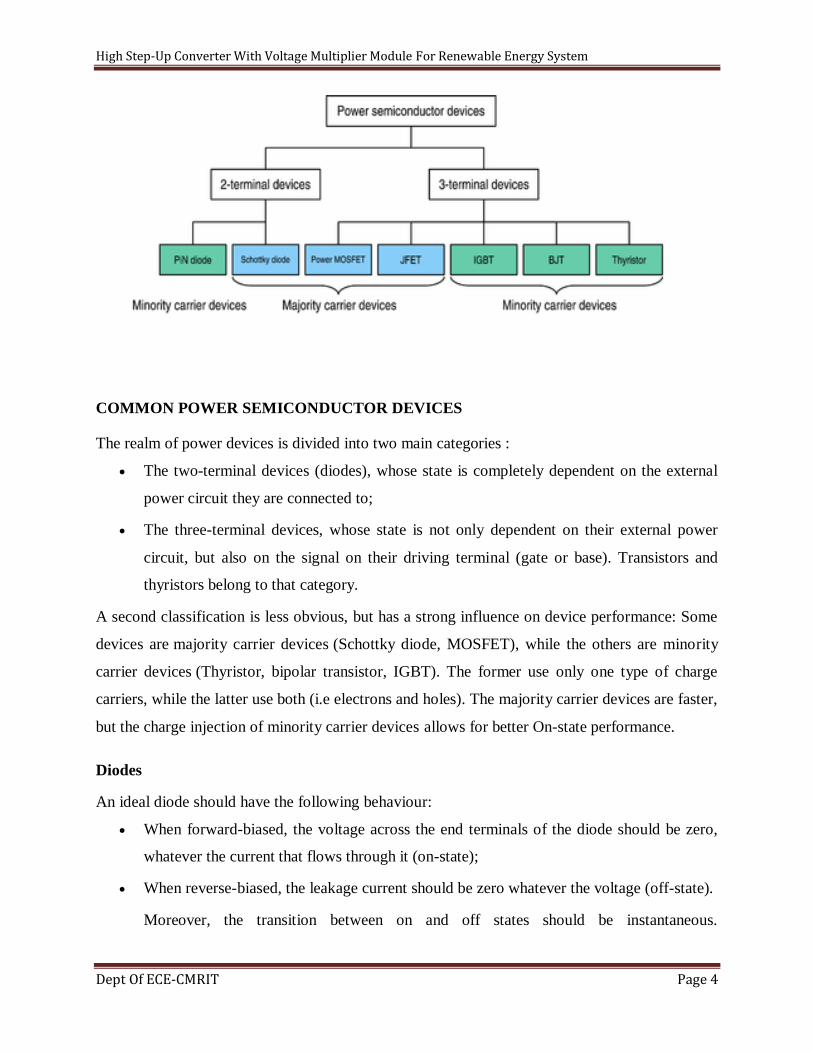
COMMON POWER SEMICONDUCTOR DEVICES
The realm of power devices is divided into two main categories :
The two-terminal devices (diodes), whose state is completely dependent on the external
power circuit they are connected to;
The three-terminal devices, whose state is not only dependent on their external power
circuit, but also on the signal on their driving terminal (gate or base). Transistors and
thyristors belong to that category.
A second classification is less obvious, but has a strong influence on device performance: Some
devices are majority carrier devices (Schottky diode, MOSFET), while the others are minority
carrier devices (Thyristor, bipolar transistor, IGBT). The former use only one type of charge
carriers, while the latter use both (i.e electrons and holes). The majority carrier devices are faster,
but the charge injection of minority carrier devices allows for better On-state performance.
Diodes
An ideal diode should have the following behaviour:
When forward-biased, the voltage across the end terminals of the diode should be zero,
whatever the current that flows through it (on-state);
When reverse-biased, the leakage current should be zero whatever the voltage (off-state).
Moreover, the transition between on and off states should be instantaneous.
High Step-Up Converter With Voltage Multiplier Module For Renewable Energy System
Dept Of ECE-CMRIT Page 5
In reality, the design of a diode is a trade-off between performance in on-state, off-state
and commutation. Indeed, it is the same area of the device that has to sustain the blocking
voltage in off-state and allow current flow in the on-state. As the requirements for the two state
are completely opposite, it can be intuitively seen that a diode has to be either optimised for one
of them, or time must be allowed to switch from one state to the other.
This trade-off between on-state, off-state and switching speed is the same for all power
devices. A Schottky diode has excellent switching speed and on-state performance, but a high
level of leakage current in off-state. PiN diodes are commercially available in different
commutation speeds but any increase in speed is paid by lower performance in on-state.
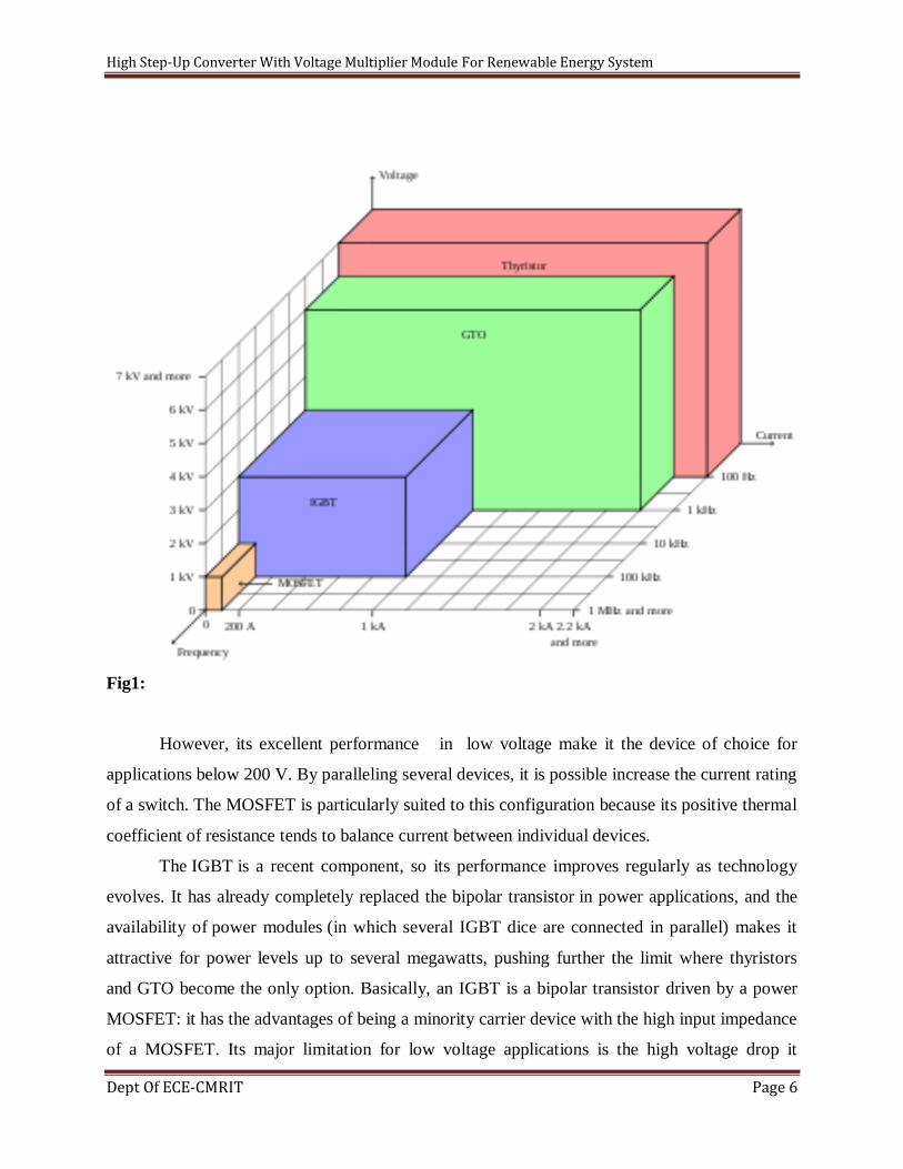
Switches:
The trade-off between voltage, current and frequency ratings also exists for the switches.
Actually, all power semiconductors rely on a PiN diode structure to sustain voltage. This can be
seen in figure 2. The power MOSFET has the advantages of the majority carrier devices, so it
can achieve very high operating frequency, but can't be used with high voltages. As it is a
physical limit, no improvement is expected from silicon MOSFET concerning their maximum
Voltage ratings.
High Step-Up Converter With Voltage Multiplier Module For Renewable Energy System
Dept Of ECE-CMRIT Page 6
Fig1:
However, its excellent performance in low voltage make it the device of choice for
applications below 200 V. By paralleling several devices, it is possible increase the current rating
of a switch. The MOSFET is particularly suited to this configuration because its positive thermal
coefficient of resistance tends to balance current between individual devices.
The IGBT is a recent component, so its performance improves regularly as technology
evolves. It has already completely replaced the bipolar transistor in power applications, and the
availability of power modules (in which several IGBT dice are connected in parallel) makes it
attractive for power levels up to several megawatts, pushing further the limit where thyristors
and GTO become the only option. Basically, an IGBT is a bipolar transistor driven by a power
MOSFET: it has the advantages of being a minority carrier device with the high input impedance
of a MOSFET. Its major limitation for low voltage applications is the high voltage drop it
High Step-Up Converter With Voltage Multiplier Module For Renewable Energy System
Dept Of ECE-CMRIT Page 7
low , mainly because of a so-called 'current-tail' problem during turn-off. This problem is caused
by the slow decay of the conduction current during turn-off resulting from slow recombination of
large number of carriers, which flood the thick 'drift' region of the IGBT during conduction. The
net result is that the turn-off switching loss of an IGBT is considerably higher than its turn-on
loss. Generally, in datasheet, turn-off energy is mentioned as a measured parameter and one has
to multiply that number with the switching frequency of the intended application to estimate the
turn-off loss.
At very high power levels, thyristor-based devices are still the only choice. Though
driving a thyristor is somewhat complicated, as this device can only be turned on. It turns off by
itself as soon as no more current flows through it. This requires specific circuit with means to
divert current, or specific applications where current is known to cancel regularly. Different
solution have been developed to overcome this limitation. These components are widely used
in power distribution applications.
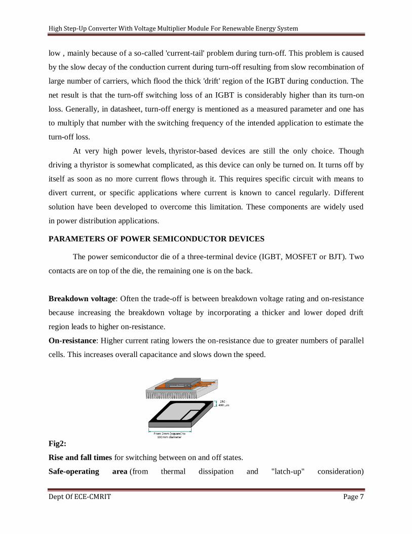
PARAMETERS OF POWER SEMICONDUCTOR DEVICES
The power semiconductor die of a three-terminal device (IGBT, MOSFET or BJT). Two
contacts are on top of the die, the remaining one is on the back.
Breakdown voltage: Often the trade-off is between breakdown voltage rating and on-resistance
because increasing the breakdown voltage by incorporating a thicker and lower doped drift
region leads to higher on-resistance.
On-resistance: Higher current rating lowers the on-resistance due to greater numbers of parallel
cells. This increases overall capacitance and slows down the speed.
Fig2:
Rise and fall times for switching between on and off states.
Safe-operating area (from thermal dissipation and "latch-up" consideration)
High Step-Up Converter With Voltage Multiplier Module For Renewable Energy System
Dept Of ECE-CMRIT Page 8
Thermal resistance: This is actually an often-ignored but extremely important parameter from
practical system design point of view. Semiconductors do not perform well at elevated
temperature but due to large current conduction, all power semiconductor device heat up.
Therefore it needs to be cooled by removing that heat continuously. Packaging interface provides
the path between the semiconductor device and external world to channelize the heat outside.
Generally, large current devices have large die and packaging surface area and lower thermal
resistance.
TRIS bit to make a pin an output, while other peripherals override the TRIS bit to make a
pin an input.
EXISTING SYSTEM:
Nowadays, renewable energy is increasingly valued and employed worldwide because of energy
shortage and environmental contamination. Renewable energy systems generate low voltage
output, and thus, high step-up dc/dc converters have been widely employed in many renewable
energy applications such fuel cells, wind power generation, and photovoltaic (PV) systems. Such
systems transform energy from renewable sources into electrical energy and convert low voltage
into high voltage via a step-up converter.The high step-up conversion may require two-stage
converters with cascade structure for enough step-up gain, which decreases the efficiency and
increases the cost. Thus, a high step-up converter is seen as an important stage in the system
because such a system requires a sufficiently high step-up conversion.
PROPOSED SYSTEM:
Multiplier module, and the voltage multiplier module is composed of switched capacitors and
coupled inductors. The coupled inductors can be designed to extend step-up gain, and the
switched capacitors offer extra voltage conversion ratio. In addition, when one of the switches
turns off, the energy stored in the magnetizing inductor will transfer via three respective paths;
thus, the current distribution not only decreases the conduction losses by lower effective current
High Step-Up Converter With Voltage Multiplier Module For Renewable Energy System
Dept Of ECE-CMRIT Page 9
but also makes currents through some diodes decrease to zero before they turn off, which
alleviate diode reverse recovery losses. The advantages of the proposed converter are as follows.
1) The proposed converter is characterized by low input current ripple and low conduction
losses, which increases the lifetime of renewable energy sources and makes it suitable for high-
power applications. 2) The converter achieves the high step-up gain that renewable energy
systems require. 3) Due to the lossless passive clamp performance, leakage energy is recycled to
the output terminal. Hence, large voltage spikes across the main switches are alleviated, and the
efficiency is improved. 4) Low cost and high efficiency are achieved by employment of the low-
voltage-rated power switch with low RDS (ON); also, the voltage stresses on main switches and
diodes are substantially lower than output voltage. 5) The inherent configuration of the proposed
converter makes some diodes decrease conduction losses and alleviate diode reverse recovery
losses.
High Step-Up Converter With Voltage Multiplier Module For Renewable Energy System
Dept Of ECE-CMRIT Page 10
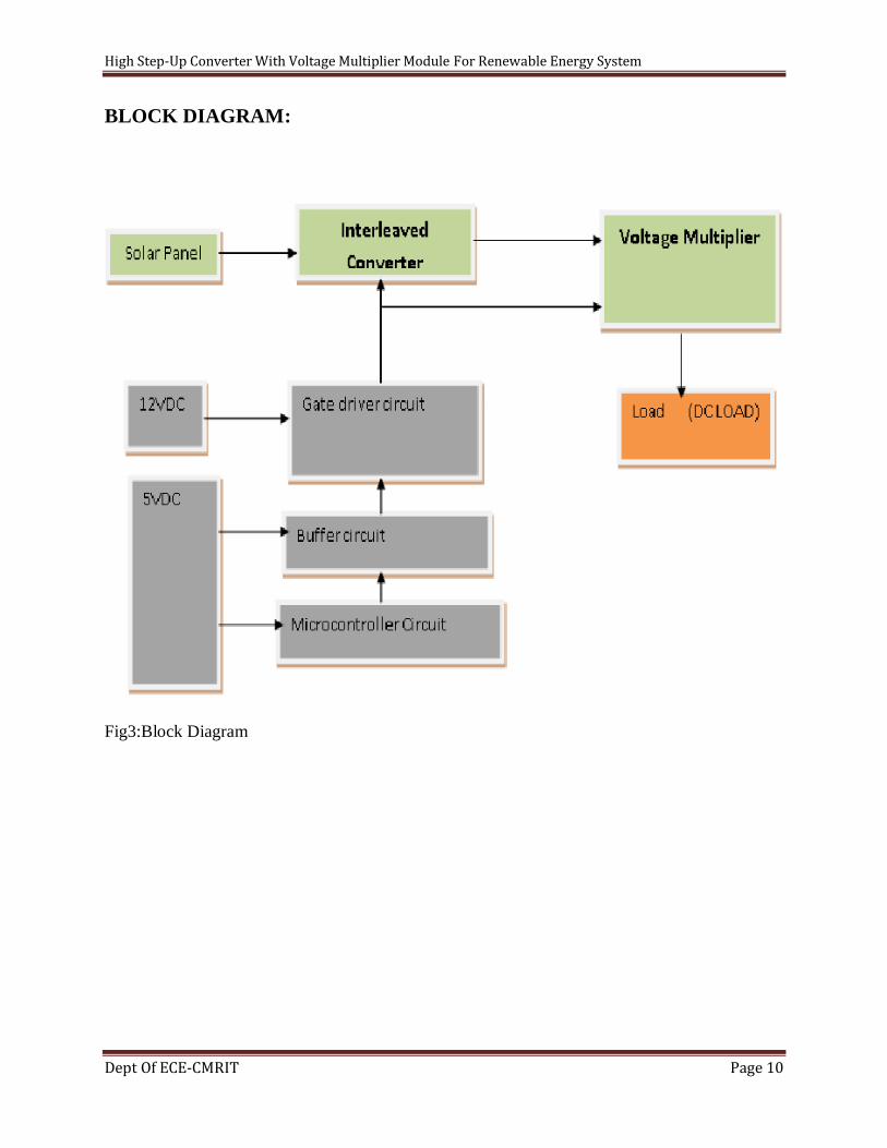
BLOCK DIAGRAM:
Fig3:Block Diagram
High Step-Up Converter With Voltage Multiplier Module For Renewable Energy System
Dept Of ECE-CMRIT Page 11
CHAPTER 2
LITERATURE SURVEY
TITLE: Design of a High Step-up DC-DC Power Converter with Voltage Multiplier Cells and
Reduced Losses on Semiconductors for Photovoltaic Systems
AUTHOR: Mamdouh L. Alghaythi ; Robert M. O’Connell ; Naz E. Islam
YEAR:2019
A high step-up dc-dc converter based on an isolated dc-dc converter with voltage
multiplier cells for photovoltaic systems is essentially introduced in this paper. The proposed
converter can provide a high step-up voltage gain. The switch voltage stress and losses on
semiconductors are significantly reduced through this work Furthermore, the proposed converter
can reliably offer and provide continuous input current which can be basically used for
integrating photovoltaic systems to convert 30 V to 480 V dc bus. The ripple on the input current
is minimized due to the isolated converter, and the proposed converter is fed by a single input
voltage. The operation modes and the characteristics of the aforementioned converter are
thoroughly analyzed. The components selection, simulation results and experiment results are
mainly verified by using MATALB Simulink. Consequently, a 360W hardware prototype is
implemented to validate the design and the theory.
TITLE: High Step-Up Interleaved Converter With Three-Winding Coupled Inductors and
Voltage Multiplier Cells
AUTHOR: Shin-Ju Chen ; Sung-Pei Yang ; Chao-Ming Huang ; Yu-Hua Chen
YEAR: 2016
High Step-Up Converter With Voltage Multiplier Module For Renewable Energy System
Dept Of ECE-CMRIT Page 12
In this paper, a novel interleaved high step-up DC-DC converter with three-winding
coupled inductors and voltage multiplier cells is proposed for renewable energy systems. The
voltage-lift and voltage-stack methods are used to extend the voltage conversion ratio. The
converter achieves high voltage gain without operating at extreme duty ratio. The voltage stress
on the power switches is greatly lower than the output voltage. As a result, the low-voltage-rated
MOSFETs with low conducting resistances can be employed to reduce the conduction losses.
The diodes reverse-recovery problem can be alleviated by the leakage inductances of the coupled
inductors. The input current ripple is reduced by the interleaved operation. The leakage energy of
the coupled inductors is recycled such that the switch turn-off voltage spikes are avoided. The
operating principles and performance analysis of the proposed converter are presented in detail.
Finally, a 1000 W experimental prototype with 28 V input and 380 V output is built and tested.
The experimental result are provided to validate the theoretical analysis and effectiveness of the
proposed converter.
TITLE: A dual-active-bridge converter-based high step-up converter with voltage-multiplier
for high-efficiency PV application
AUTHOR: Yangjun Lu ; Hongfei Wu ; Yan Xing ; Kai Sun
YEAR:2015
A high step-up soft-switching converter based on combination of a dual-active-bridge
(DAB) converter and a voltage multiplier is proposed for high efficiency photovoltaic (PV)
applications. With dual-phase-shift modulation, zero-voltage-switching (ZVS) can be realized
for both primary-side and secondary-side MOSFETs in a wide load range and the reverse
recovery problem of rectifier diodes can be eliminated naturally, which helps high efficiency
conversion be achieved. Meanwhile, leakage inductance of transformer is utilized for power
transfer and the voltage spike problem caused by leakage inductance is overcome. Owe to use of
power transfer inductor and voltage multiplier, the voltage stresses of primary-side and
secondary-side power devices are clamped to the input voltage and half of output voltage. The
High Step-Up Converter With Voltage Multiplier Module For Renewable Energy System
Dept Of ECE-CMRIT Page 13
operation principle is analyzed in detail and experimental results with a 500W, 40-56V to 380V
prototype are provided to verify the effectiveness and advantages of the proposed converter.
TITLE: Interleaved high step-up DC-DC converter with parallel-input series-output
configuration and voltage multiplier module
AUTHOR: Shin-Ju Chen ; Sung-Pei Yang ; Chao-Ming Huang ; Chuan-Kai Lin
YEAR:2017
An interleaved high step-up dc-dc converter is proposed for high voltage gain and high
efficiency applications. The configuration is composed of modified two-phase interleaved boost
converter with parallel-input series-output connection and a voltage multiplier module stacking
on the output side. In the proposed converter, the parallel-input connection is used to share the
input current and to reduce the conduction losses, while the series-output connection and voltage
multiplier module are employed to obtain the high voltage gain without operating at extreme
duty ratio. In addition, the input current ripple is reduced due to the interleaved operation. The
voltage stresses on the power switches are greatly lower than the output voltage such that the
low-voltage-rated MOSFETs with low conduction resistor are available to reduce the conduction
losses and to improve the conversion efficiency. Meanwhile, the output diode reverse-recovery
problem is alleviated by the leakage inductance of the coupled inductors. Finally, the
experimental results from a 1-kW prototype are provided to validate the effectiveness of the
proposed converter.
TITLE: A novel high step-up multilevel boost converter using double voltage-lift switched-
inductor cell
AUTHOR: Mahajan Sagar Bhaskar ; Nandyala Sreeramula Reddy ; Repalle Kusala Pavan
Kumar ; Y. Bhaskar S S Gupt
YEAR:2015
High Step-Up Converter With Voltage Multiplier Module For Renewable Energy System
Dept Of ECE-CMRIT Page 14
In this paper a novel high step-up multilevel boost converter using double voltage-lift
switched-inductor (D-VLSI) cell is proposed. Series connection of conventional DC-DC boost
converter is not a proper solution to achieve high voltage gain. Thus, DC-DC multilevel
converters are employed to achieve high voltage gain. The proposed high step-up multilevel
boost converter is a combination of double voltage-lift switched-inductor (D-VLSI) cell and
voltage multiplier cell. In this paper double voltage-lift switched-inductor (D-VLSI) cell is used
to enhance the step-up capability of multilevel DC-DC converter. Two switches, 2N+3 diodes,
2N+1 capacitor and two inductors are required to design the proposed N-level high step-up
multilevel boost converter topology. Proposed high step-up multilevel converter circuit can be
designed by using low voltage rating devices because blocking voltage across each power
devices is low. The main advantage of proposed converter circuit is high voltage is achieved
without using transformer, coupled inductor and high duty cycle. The gain of proposed
multilevel converter is depends upon the duty ratio and levels present in voltage multiplier cell.
Proposed DC-DC converter is designed for unidirectional power transfer applications. The
proposed high step-up multilevel converter has been designed for three levels with rated power
300W, output voltage is 324V, input supply voltage is 12V, and switching frequency is 50kHz.
The proposed high step-up multilevel converter circuit is simulated in MATLAB/SEVIULINK.
TITLE: High Power High Step-up DC/DC Converter Based on Multiple Input-Terminal
Voltage Multiplier
AUTHOR: Binxin Zhu ; Han Wang ; Yao Chen ; Mahinda Vilathgamuwa
YEAR:2019
Voltage multipliers (VMs) are widely used to combine with traditional DC/DC converter to
achieve high voltage conversion gain. However, the input-terminals of existing VM circuits are
unchangeable to two which make these converters are not suitable for high power/current
applications. In this paper, a high power high step-up DC/DC converter based on multiple input-
terminal voltage multiplier (MIVM) is presented. Analysis of the operation principles and the
performance characteristics of the proposed converter are presented in detail. And an
experimental prototype with a rated power of 800W was built to verify the correctness of the
theory.

High Step-Up Converter With Voltage Multiplier Module For Renewable Energy System
Dept Of ECE-CMRIT Page 15
CHAPTER 3
COMPONENT DESCRIPTION
PIC16F877A:
The term PIC, or Peripheral Interface Controller, is the name given by Microchip
Technologies to its single – chip microcontrollers. PIC micros have grown to become the most
widely used microcontrollers in the 8- bit microcontroller segment.
The PIC16F877A CMOS FLASH-based 8-bit microcontroller is upward compatible with
the PIC16C5x, PIC12Cxxx and PIC16C7x devices. It features 200 ns instruction execution, 256
bytes of EEPROM data memory, self programming, an ICD, 2 Comparators, 8 channels of 10-bit
Analog-to-Digital (A/D) converter, 2 capture/compare/PWM functions, a synchronous serial port
that can be configured as either 3-wire SPI or 2-wire I2C bus, a USART, and a Parallel Slave
Port.
Special Microcontroller Features
Flash Memory: 14.3 Kbytes (8192 words)
Data SRAM: 368 bytes
Data EEPROM: 256 bytes
Self-reprogrammable under software control
In-Circuit Serial Programming via two pins (5V)
Watchdog Timer with on-chip RC oscillator
Programmable code protection
Power-saving Sleep mode
In-Circuit Debug via two pins
10-bit, 8-channel A/D Converter
Brown-Out Reset
Analog Comparator module
Peripheral Features
High Step-Up Converter With Voltage Multiplier Module For Renewable Energy System
Dept Of ECE-CMRIT Page 16
33 I/O pins; 5 I/O ports
Timer0: 8-bit timer/counter with 8-bit prescaler
Timer1: 16-bit timer/counter with prescaler
o Can be incremented during Sleep via external crystal/clock
Timer2: 8-bit timer/counter with 8-bit period register, prescaler and postscaler
Two Capture, Compare, PWM modules
o 16-bit Capture input; max resolution 12.5 ns
o 16-bit Compare; max resolution 200 ns
o 10-bit PWM
Synchronous Serial Port with two modes:
o SPI Master
o I2C Master and Slave
USART/SCI with 9-bit address detection
Parallel Slave Port (PSP)
o 8 bits wide with external RD, WR and CS controls
Brown-out detection circuitry for Brown-Out Reset
The internal block diagram of PIC16F877 is shown in the figure. It contains 4-
banks of register files such as Bank 0, Bank 1, Bank 2 and Bank 3 from 00h-07h, 80h-
FFh, 100h-17Fh and 180h-1FFh respectively. And it is also having program FLASH
memory, Data memory and Data EEPROM of 8K, 368 and 256 Bytes respectively.
Register File
The term register file in PIC terminology used to denote the locations than an instruction
can access via an address. The register file consists of two components, they are
1. General purpose register file
2. Special purpose register file
High Step-Up Converter With Voltage Multiplier Module For Renewable Energy System
Dept Of ECE-CMRIT Page 17
General Purpose Register File
The general-purpose register file is another name for the microcontrollers RAM. Data
can be written to each 8-bit location, updated and retrieved any number of times. All control
registers are coming under the general purpose register file.
Special Purpose Register File
The special purpose register file contains input and output ports as well as the control
registers used to establish each bit of port as either an input or output. It contains registers that
provide the data input and data output to the variety of resources on the chip, such as the timers,
the serial ports and the analog–to–digital converter.
The pins RB0-RB7, RC0-RC7, and RD0-RD7 are digital I/O pins. The pins CCP1 and
CCP2, which share locations with RC1 and RC2, can be used for a PWM signal (see DC Motor
tutorial). The pins AN0-AN7 are for analog I/O (see Photo resistor tutorial). TX and RX are for
debugging I/O (see Output Messages to Computer tutorial). The remaining pins deal with
power/ground, the clock signal, and programmer I/O.
A PIC is made of several “ports.” Each port is designated with a letter, RB0-RB7 are a port.
RC0-RC7 and RD0-RD7 are a port as well. RA0-RA5 and RE0-RE2 are also ports, but with
fewer pins. Some of these pins have special purposes, but most can be used as basic input/output
pins.
For example, you can set pin RB0 to be either an input pin, or an output pin. As an input
pin, the digital voltage on the pin can be read in. For example, if RB0 is connected to ground
(0v), then you would read a digital 0. If RB0 was connected to power (5v), then you would read
a digital 1.
On the other hand, if you wanted to set RBO as an output pin, you could choose to make
RB0 either be 5v, or 0v. This can be used, for example, to turn off or on a LED, or to turn off or
on a motor.
High Step-Up Converter With Voltage Multiplier Module For Renewable Energy System
Dept Of ECE-CMRIT Page 18
Fig4:Pin Configuration and Description

High Step-Up Converter With Voltage Multiplier Module For Renewable Energy System
Dept Of ECE-CMRIT Page 19
Memory Organization
There are three memory blocks in each of the PIC16F87XA devices. The Program
Memory and Data Memory have separate buses so that concurrent access.
Program Memory Organization
The PIC16F87XA devices have a 13-bit program counter capable of addressing an 8K
word x 14 bit program memory space. The PIC16F876A/877A devices have 8K words x 14 bits
of FLASH program memory, while PIC16F873A/874A devices have 4K words x 14 bits.
Accessing a location above the physically implemented address will cause a wraparound. The
RESET vector is at 0000h and the interrupt vector is at 0004h.
Data Memory Organization
High Step-Up Converter With Voltage Multiplier Module For Renewable Energy System
Dept Of ECE-CMRIT Page 20
The data memory is partitioned into multiple banks which contain the General Purpose
Registers and the Special Function Registers. Bits RP1 (STATUS<6>) and RP0 (STATUS<5>)
are the bank select bits.
Fig6:
High Step-Up Converter With Voltage Multiplier Module For Renewable Energy System
Dept Of ECE-CMRIT Page 21
Each bank extends up to 7Fh (128 bytes). The lower locations of each bank are reserved
for the Special Function Registers. Above the Special Function Registers are General Purpose
Registers, implemented as static RAM. All implemented banks contain Special Function
Registers. Some frequently used Special Function Registers from one bank may be mirrored in
another bank for code reduction and quicker access.
NAME FUNCTION ADDRESS
RAM ADDRESS
BIT
ADDRESABLE
STATUS Status register 03H,83H,103H,183H Yes
FSR File select register 04H,84H,104H,184H Yes
PORTA I/O latch 05H Yes
PORTB I/O latch 06H Yes
PORTC I/O latch 07H Yes
PORTD I/O latch 08H Yes
PORTE I/O latch 09H Yes
INTCON Interrupt control
register
0BH,8BH,10BH,18BH Yes
PIR1 Peripheral interrupt 0CH Yes
RCSTA Receive status and 18H Yes

High Step-Up Converter With Voltage Multiplier Module For Renewable Energy System
Dept Of ECE-CMRIT Page 22
control register
TXREG Transmit register 19H Yes
RCREG Receive register 1AH Yes
OPTION_REG Optional register 81H Yes
TRISA I/O register 85H Yes
TRISB I/O register 86H Yes
TRISC I/O register 87H Yes
TRISD I/O register 88H Yes
TRISE I/O register 89H Yes
TXSTA Transmit status and
control register
98H Yes
High Step-Up Converter With Voltage Multiplier Module For Renewable Energy System
Dept Of ECE-CMRIT Page 22
ADDRESSING MODES
Direct Addressing
Using this method we are accessing the registers directly by detecting location inside
Data Memory from Opcode and by selecting the bank using bits RP1 and RP0 of the STATUS
register.
Indirect Addressing
To implement indirect addressing, a File Select Register (FSR) and indirect register
(INDF) are used. In addition, when using this method we choose bank using bit IRP of the
STATUS register. Indirect addressing treated like a stack pointer, allowing much more efficient
work with a number of variables. INDF register is not an actual register (it is a virtual register
that is not found in any bank).
High Step-Up Converter With Voltage Multiplier Module For Renewable Energy System
Dept Of ECE-CMRIT Page 23
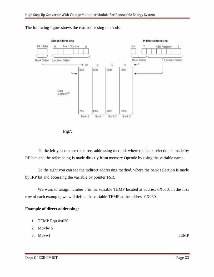
The following figure shows the two addressing methods:
Fig7:
To the left you can see the direct addressing method, where the bank selection is made by
RP bits and the referencing is made directly from memory Opcode by using the variable name.
To the right you can see the indirect addressing method, where the bank selection is made
by IRP bit and accessing the variable by pointer FSR.
We want to assign number 5 to the variable TEMP located at address 0X030. In the first
row of each example, we will define the variable TEMP at the address 0X030.
Example of direct addressing:
1. TEMP Equ 0x030
2. Movlw 5
3. Movwf TEMP

High Step-Up Converter With Voltage Multiplier Module For Renewable Energy System
Dept Of ECE-CMRIT Page 24
It's easy to understand, that direct addressing method means working directly with the
variables. In the second line we put the number 5 into the working register W, and in the line 3,
the content of the W passes to the TEMP variable.
Example of indirect addressing:
1. TEMP Equ 0x030
2. Movlw 0x030
3. Movwf FSR
4. Movlw 5
5. Movwf INDF
In the second line, we put a value into the W register. In the third line, the value passes to
the FSR register, and from this moment FSR points to the address of the TEMP variable. In the
fourth line, the number 5 passes to the W register, and in the fifth line, we move the contents of
W register (which is 5) to the INDF. In fact INDF performs the following: it takes the number 5
and puts it in the address indicated by FSR register.
PIC16F87XA Data EEPROM
The data EEPROM and Flash program memory is readable and writable during normal
operation (over the full VDD range). This memory is not directly mapped in the register file
space. Instead, it is indirectly addressed through the Special Function Registers.
There are six SFRs used to read and write to this memory:
1. EECON1
2. EECON2
3. EEDATA
4. EEDATH
5. EEADR
6. EEADRH
High Step-Up Converter With Voltage Multiplier Module For Renewable Energy System
Dept Of ECE-CMRIT Page 25
When interfacing to the data memory block, EEDATA holds the 8-bit data for read/write
and EEADR holds the address of the EEPROM location being accessed. These devices have 128
or 256 bytes of data EEPROM (depending on the device), with an address range from 00h to
FFh. On devices with 128 bytes, addresses from 80h to FFH are unimplemented.
A few important points about Data EEPROM memory:
It lets you save data DURING programming
The data is saved during the “burning” process
You can read the data memory during the programming and use it
The use is made possible with the help of SFR
At this point there is no need to learn how to use this memory with special registers,
because there are functions (writing and reading) that are ready.
Write to DATA EEPROM
To write to an EEPROM data location, the user must first write the address to the
EEADR register and the data to the EEDATA register. Then the user must follow a specific
write sequence to initiate the write for each byte.
Read DATA EEPROM
To read a data memory location, the user must write the address to the EEADR register,
clear the EEPGD control bit (EECON1<7>) and then set control bit RD (EECON1<0>). The
data is available in the very next cycle in the EEDATA register; therefore, it can be read in the
next instruction. EEDATA will hold this value until another read or until it is written to by the
user (during a write operation).
Both of these functions are provided by the manufacturer. There is a required sequence in
order to write/read to/from the memory; that process can be performed independently, but it is
better to use ready functions of Microchip.

High Step-Up Converter With Voltage Multiplier Module For Renewable Energy System
Dept Of ECE-CMRIT Page 26
PIC Timer0:
Many times, we plan and build systems that perform various processes that depend on
time.
Simple example of this process is the digital wristwatch. The role of this electronic
system is to display time in a very precise manner and change the display every second (for
seconds), every minute (for minutes) and so on.
To perform the steps we've listed, the system must use a timer, which needs to be very
accurate in order to take necessary actions. The clock is actually a core of any electronic system.
In this PIC timer module tutorial we will study the existing PIC timer modules. The
microcontroller PIC16F877 has 3 different timers:
PIC Timer0
PIC Timer1
PIC Timer2
We can use these timers for various important purposes. So far we used “delay
procedure” to implement some delay in the program, that was counting up to a specific value,
before the program could be continued. "Delay procedure" had two disadvantages:
we could not say exactly how long the Delay procedure was in progress
we could not perform any further steps while the program executes the "delay procedure"
Now, using Timers we can build a very precise time delays which will be based on the
system clock and allow us to achieve our desired time delay well-known inadvance. In order for
us to know how to work with these timers, we need to learn some things about each one of them.
We will study each one separately. PIC Timer0
The Timer0 module timer/counter has the following features:
8-bit timer/counter
High Step-Up Converter With Voltage Multiplier Module For Renewable Energy System
Dept Of ECE-CMRIT Page 27
Readable and writable
8-bit software programmable prescaler
Internal (4 Mhz) or external clock select
Interrupt on overflow from FFh to 00h
Edge select (rising or falling) for external clock
Timer0 has a register called TMR0 Register, which is 8 bits of size.
We can write the desired value into the register which will be increment as the program
progresses. Frequency varies depending on the Prescaler. Maximum value that can be
assigned to this register is 255.
PIC Timer1:
The Timer1 module, timer/counter, has the following features:
16-bit timer/counter consisting of two 8-bit registers (TMR1H and TMR1L)
readable and writable
8-bit software programmable prescaler
Internal (4 Mhz) or external clock select
Interrupt on overflow from FFFFh to 0000h
Timer1 has a register called TMR1 register, which is 16 bits of size.
Actually, the TMR1 consists of two 8-bits registers:
TMR1H
TMR1L
It increments from 0000h to the maximum value of 0xFFFFh (or 0 b1111 1111 1111
1111 or 65,535 decimal). The TMR1 interrupt, if enabled, is generated on overflow
which is latched in interrupt flag bit, TMR1IF (PIR1<0>). This interrupt can be
enabled/disabled by setting/clearing TMR1 interrupt enable bit, TMR1IE (PIE1<0>).
You can initialize the value of this register to what ever you want (not necessarily "0").
TMR1IF – TMR1 overflow Interrupt Flag bit.
High Step-Up Converter With Voltage Multiplier Module For Renewable Energy System
Dept Of ECE-CMRIT Page 28
This flag marks the end of ONE cycle count. The flag need to be reset in the software if
you want to do another cycle count. We can read the value of the register TMR1 and write into.
We can reset its value at any given moment (write) or we can check if there is a certain numeric
value that we need (read).
Prescaler – Frequency divider.
We can use Prescaler for further division of the system clock. The size of the register is 2-
bit only, so you can make four different division. The options are:
1:1
1:2
1:4
1:8
You can choose whether to use an internal system clock (crystal) or external oscillator
that can be connected to a pin RC0.
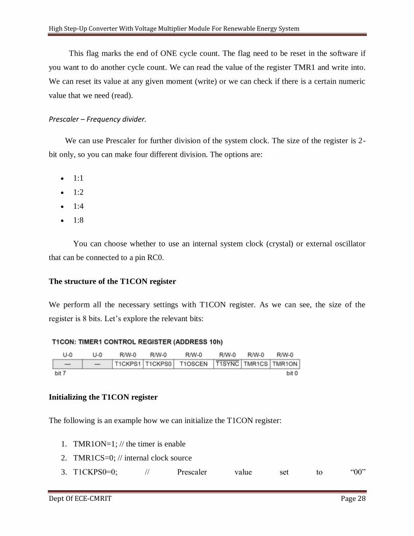
The structure of the T1CON register
We perform all the necessary settings with T1CON register. As we can see, the size of the
register is 8 bits. Let’s explore the relevant bits:
Initializing the T1CON register
The following is an example how we can initialize the T1CON register:
1. TMR1ON=1; // the timer is enable
2. TMR1CS=0; // internal clock source
3. T1CKPS0=0; // Prescaler value set to “00”
High Step-Up Converter With Voltage Multiplier Module For Renewable Energy System
Dept Of ECE-CMRIT Page 29
4. T1CKPS1=0; // which means 1:1 (no division)
Or you can set all the T1CON register at once as follows:
T1CON=0b00000001;
PIC Timer2:
The Timer2module has the following features:
Two 8-bit registers (TMR2 and PR2) readable and writable prescaler and a
postscaler connected only to an internal clock - 4 MHz crystal Interrupt on overflow
• Timer2 has 2 count registers: TMR2 and PR2. The size of each registers is 8-bit in
which we can write numbers from 0 to 255. The TMR2 register is readable and writable
and is cleared on any device Reset. PR2 is a readable and writable register and initialized
to FFh upon Reset.
Register TMR2 is used to store the “initial” count value (the value from which it
begins to count). Register PR2 is used to store the “ending” count value (the maximum
value we need/want to reach). ie: using Timer2 we can determine the started count value,
the final count value, and the count will be between these two values. The Timer2
increment from 00h until it matches PR2 and then resets to 00h on the next increment
cycle.
• Prescaler and Postscaler - Timer2 is an 8-bit timer with a prescaler and a postscaler. Each
allows to make additional division of the frequency clock source. Prescaler divides the
frequency clock source BEFORE the counting take place at the register TMR2, thus the
counting inside the TMR2 register is performed based on the divided frequency clock
source by the Prescaler The match output of TMR2 goes through a 4-bit postscaler
(which gives a 1:1 to 1:16 scaling inclusive) to generate a TMR2 interrupt (latched in flag
bit, TMR2IF(PIR1<1>)).Postscaler divides the frequency that comes out of the
Comparator again for the last time.
High Step-Up Converter With Voltage Multiplier Module For Renewable Energy System
Dept Of ECE-CMRIT Page 30
INPUT/OUTPUT PROGRAMMING IN PIC16F877A
Introduction
General purpose I/O pins can be considered the simplest of peripherals. They allow the
PIC microcontroller to monitor and control other devices. To add flexibility and functionality to
a device, some pins are multiplexed with an alternate function(s). These functions depend on
which peripheral features are on the device. In general, when a peripheral is functioning, that pin
may not be used as a general purpose I/O pin.
For most ports, the I/O pin’s direction (input or output) is controlled by the data direction
register, called the TRIS register. TRIS<x> controls the direction of PORT<x>. A ‘1’ in the
TRIS bit corresponds to that pin being an input, while a ‘0’ corresponds to that pin being an
output. An easy way to remember is that a ‘1’ looks like I (input) and a ‘0’ looks like an O
output).
The PORT register is the latch for the data to be output. When the PORT is read, the
device reads the levels present on the I/O pins (not the latch). This means that care should be
taken with read-modify-write commands on the ports and changing the direction of a pin from an
input to an output.
Reading the PORT register reads the status of the pins whereas writing to it will write to
the port latch. All write operations (such as BSF and BCF instructions) are read-modify-write
operations. Therefore a write to a port implies that the port pins are read; this value is modified,
and then written to the port data latch.
When peripheral functions are multiplexed onto general I/O pins, the functionality of the
I/O pins may change to accommodate the requirements of the peripheral module. Examples of
this are the Analog-to-Digital (A/D) converter and LCD driver modules, which force the I/O pin
to the peripheral function when the device is reset. In the case of the A/D, this prevents the
device from consuming excess current if any analog levels were on the A/D pins after a reset
occurred.
With some peripherals, the TRIS bit is overridden while the peripheral is enabled.
Therefore, read-modify-write instructions (BSF, BCF, XORWF) with TRIS as destination should
High Step-Up Converter With Voltage Multiplier Module For Renewable Energy System
Dept Of ECE-CMRIT Page 31
be avoided. The user should refer to the corresponding peripheral section for the correct
TRIS bit settings.
PORT pins may be multiplexed with analog inputs and analog VREF input. The
operation of each of these pins is selected, to be an analog input or digital I/O, by clearing/setting
the control bits in the ADCON1 register (A/D Control Register1). When selected as an analog
input, these pins will read as ‘0’s.
The TRIS registers control the direction of the port pins, even when they are being used
as analog inputs. The user must ensure the TRIS bits are maintained set when using the pins as
analog inputs.
PORTA and the TRISA Register
The RA4 pin is a Schmitt Trigger input and an open drain output. All other RA port pins
have TTL input levels and full CMOS output drivers. All pins have data direction bits (TRIS
registers) which can configure these pins as output or input.
Setting a TRISA register bit puts the corresponding output driver in a hi-impedance mode.
Clearing a bit in the TRISA register puts the contents of the output latch on the selected pin(s).
PORTB and the TRISB Register
PORTB is an 8-bit wide bi-directional port. The corresponding data direction register is
TRISB. Setting a bit in the TRISB register puts the corresponding output driver in a high-
impedance input mode. Clearing a bit in the TRISB register puts the contents of the output latch
on the selected pin(s).
Each of the PORTB pins has a weak internal pull-up. A single control bit can turn on all
the pull-ups. This is performed by clearing bit RBPU (OPTION<7>). The weak pull-up is
automatically turned off when the port pin is configured as an output. The pull-ups are disabled
on a Power-on Reset.
Four of PORTB’s pins, RB7:RB4, have an interrupt on change feature. Only pins
configured as inputs can cause this interrupt to occur (i.e. any RB7:RB4 pin configured as an
output is excluded from the interrupt on change comparison). The input pins (of RB7:RB4) are

High Step-Up Converter With Voltage Multiplier Module For Renewable Energy System
Dept Of ECE-CMRIT Page 32
compared with the old value latched on the last read of PORTB. The “mismatch” outputs of
RB7:RB4 are OR’ed together to generate the RB Port Change Interrupt with flag bit RBIF
(INTCON<0>).
This interrupt can wake the device from SLEEP. The user, in the interrupt service
routine, can clear the interrupt in the following manner:
a) Any read or write of PORTB. This will end the mismatch condition.
b) Clear flag bit RBIF.
A mismatch condition will continue to set flag bit RBIF. Reading PORTB will end the
mismatch condition, and allow flag bit RBIF to be cleared. This interrupt on mismatch feature,
together with software configurable pull-ups on these four pins allow easy interface to a keypad
and make it possible for wake-up on key-depression.
The interrupt on change feature is recommended for wake-up on key depression and
operations where PORTB is only used for the interrupt on change feature. Polling of PORTB is
not recommended while using the interrupt on change feature.
PORTC and the TRISC Register
PORTC and the TRISC Register PORTC is an 8-bit bi-directional port. Each pin is
individually configurable as an input or output through the TRISC register. PORTC pins have
Schmitt Trigger input buffers. When enabling peripheral functions, care should be taken in
defining TRIS bits for each PORTC pin. Some peripherals override the TRIS bit to make a pin
an output, while other peripherals override the TRIS bit to make a pin an input.
PORTD and the TRISD Register
PORTD is an 8-bit port with Schmitt Trigger input buffers. Each pin is individually
configurable as an input or output.
High Step-Up Converter With Voltage Multiplier Module For Renewable Energy System
Dept Of ECE-CMRIT Page 33
PORTE and the TRISE Register
PORTE can be up to an 8-bit port with Schmitt Trigger input buffers. Each pin is
individually configurable as an input or output.
On some devices with PORTE, the upper bits of the TRISE register are used for the
Parallel Slave Port control and status bits.
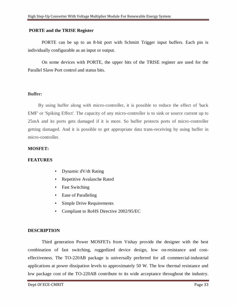
Buffer:
By using buffer along with micro-controller, it is possible to reduce the effect of 'back
EMF' or 'Spiking Effect'. The capacity of any micro-controller is to sink or source current up to
25mA and its ports gets damaged if it is more. So buffer protects ports of micro-controller
getting damaged. And it is possible to get appropriate data trans-receiving by using buffer in
micro-controller.
MOSFET:
FEATURES
• Dynamic dV/dt Rating
• Repetitive Avalanche Rated
• Fast Switching
• Ease of Paralleling
• Simple Drive Requirements
• Compliant to RoHS Directive 2002/95/EC
DESCRIPTION
Third generation Power MOSFETs from Vishay provide the designer with the best
combination of fast switching, ruggedized device design, low on-resistance and cost-
effectiveness. The TO-220AB package is universally preferred for all commercial-industrial
applications at power dissipation levels to approximately 50 W. The low thermal resistance and
low package cost of the TO-220AB contribute to its wide acceptance throughout the industry.
High Step-Up Converter With Voltage Multiplier Module For Renewable Energy System
Dept Of ECE-CMRIT Page 34
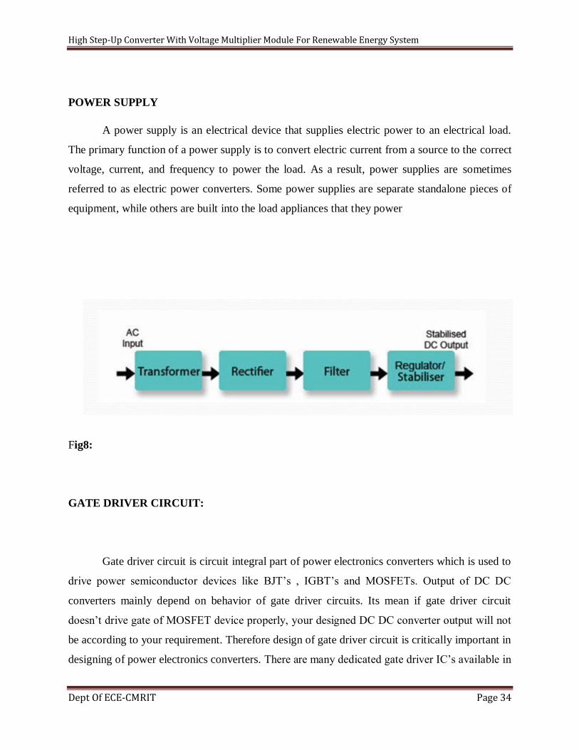
POWER SUPPLY
A power supply is an electrical device that supplies electric power to an electrical load.
The primary function of a power supply is to convert electric current from a source to the correct
voltage, current, and frequency to power the load. As a result, power supplies are sometimes
referred to as electric power converters. Some power supplies are separate standalone pieces of
equipment, while others are built into the load appliances that they power
Fig8:
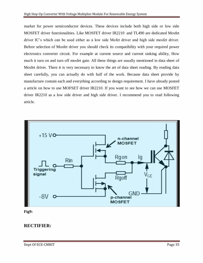
GATE DRIVER CIRCUIT:
Gate driver circuit is circuit integral part of power electronics converters which is used to
drive power semiconductor devices like BJT’s , IGBT’s and MOSFETs. Output of DC DC
converters mainly depend on behavior of gate driver circuits. Its mean if gate driver circuit
doesn’t drive gate of MOSFET device properly, your designed DC DC converter output will not
be according to your requirement. Therefore design of gate driver circuit is critically important in
designing of power electronics converters. There are many dedicated gate driver IC’s available in
High Step-Up Converter With Voltage Multiplier Module For Renewable Energy System
Dept Of ECE-CMRIT Page 35
market for power semiconductor devices. These devices include both high side or low side
MOSFET driver functionalities. Like MOSFET driver IR2210 and TL490 are dedicated Mosfet
driver IC’s which can be used either as a low side Mofet driver and high side mosfet driver.
Before selection of Mosfet driver you should check its compatibility with your required power
electronics converter circuit. For example at current source and current sinking ability, How
much it turn on and turn off mosfet gate. All these things are usually mentioned in data sheet of
Mosfet driver. There it is very necessary to know the art of data sheet reading. By reading data
sheet carefully, you can actually do with half of the work. Because data sheet provide by
manufacture contain each and everything according to design requirement. I have already posted
a article on how to use MOFSET driver IR2210. If you want to see how we can use MOSFET
driver IR2210 as a low side driver and high side driver. I recommend you to read following
article.
Fig9:
RECTIFIER:
High Step-Up Converter With Voltage Multiplier Module For Renewable Energy System
Dept Of ECE-CMRIT Page 36
A rectifier is an electrical device that converts alternating current (AC), which periodically
reverses direction, to direct current (DC), which flows in only one direction. The process is
known as rectification. Physically, rectifiers take a number of forms, including vacuum tube
diodes, mercury-arc valves, copper and selenium oxide rectifiers, semiconductor diodes, silicon-
controlled rectifiers and other silicon-based semiconductor switches. Historically, even
synchronous electromechanical switches and motors have been used. Early radio receivers,
called crystal radios, used a "cat's whisker" of fine wire pressing on a crystal of galena to serve
as a point-contact rectifier or "crystal detector".
Rectifiers have many uses, but are often found serving as components of DC power
supplies and high-voltage direct current power transmission systems. Rectification may serve in
roles other than to generate direct current for use as a source of power. As noted, detectors of
radio signals serve as rectifiers. In gas heating systems flame rectification is used to detect
presence of a flame.Because of the alternating nature of the input AC sine wave, the process of
rectification alone produces a DC current that, though unidirectional, consists of pulses of
current. Many applications of rectifiers, such as power supplies for radio, television and
computer equipment, require a steady constant DC current. In these applications the output of the
rectifier is smoothed by an electronic filter to produce a steady current. A more complex circuitry
device that performs the opposite function, converting DC to AC, is called an inverter.
While half-wave and full-wave rectification can deliver unidirectional current, neither
produces a constant voltage. Producing steady DC from a rectified AC supply requires a
smoothing circuit or filter.[6] In its simplest form this can be just a reservoir capacitor or
smoothing capacitor, placed at the DC output of the rectifier. There is still an AC ripple voltage
component at the power supply frequency for a half-wave rectifier, twice that for full-wave,
where the voltage is not completely smoothed.
Rectifier output Smoothing:
RC-Filter Rectifier: This circuit was designed and simulated using Multisim 8 software.
Sizing of the capacitor represents a trade off. For a given load, a larger capacitor reduces ripple
but costs more and creates higher peak currents in the transformer secondary and in the supply
that feeds it. The peak current is set in principle by the rate of rise of the supply voltage on the
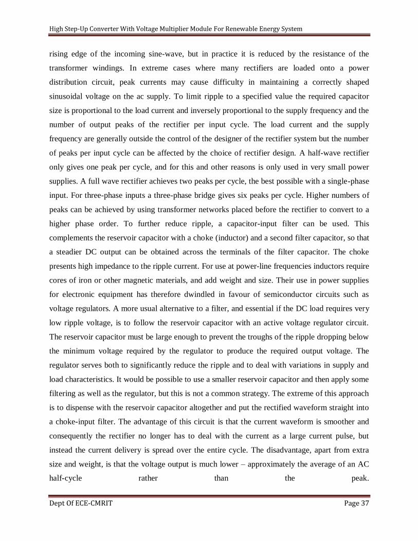
High Step-Up Converter With Voltage Multiplier Module For Renewable Energy System
Dept Of ECE-CMRIT Page 37
rising edge of the incoming sine-wave, but in practice it is reduced by the resistance of the
transformer windings. In extreme cases where many rectifiers are loaded onto a power
distribution circuit, peak currents may cause difficulty in maintaining a correctly shaped
sinusoidal voltage on the ac supply. To limit ripple to a specified value the required capacitor
size is proportional to the load current and inversely proportional to the supply frequency and the
number of output peaks of the rectifier per input cycle. The load current and the supply
frequency are generally outside the control of the designer of the rectifier system but the number
of peaks per input cycle can be affected by the choice of rectifier design. A half-wave rectifier
only gives one peak per cycle, and for this and other reasons is only used in very small power
supplies. A full wave rectifier achieves two peaks per cycle, the best possible with a single-phase
input. For three-phase inputs a three-phase bridge gives six peaks per cycle. Higher numbers of
peaks can be achieved by using transformer networks placed before the rectifier to convert to a
higher phase order. To further reduce ripple, a capacitor-input filter can be used. This
complements the reservoir capacitor with a choke (inductor) and a second filter capacitor, so that
a steadier DC output can be obtained across the terminals of the filter capacitor. The choke
presents high impedance to the ripple current. For use at power-line frequencies inductors require
cores of iron or other magnetic materials, and add weight and size. Their use in power supplies
for electronic equipment has therefore dwindled in favour of semiconductor circuits such as
voltage regulators. A more usual alternative to a filter, and essential if the DC load requires very
low ripple voltage, is to follow the reservoir capacitor with an active voltage regulator circuit.
The reservoir capacitor must be large enough to prevent the troughs of the ripple dropping below
the minimum voltage required by the regulator to produce the required output voltage. The
regulator serves both to significantly reduce the ripple and to deal with variations in supply and
load characteristics. It would be possible to use a smaller reservoir capacitor and then apply some
filtering as well as the regulator, but this is not a common strategy. The extreme of this approach
is to dispense with the reservoir capacitor altogether and put the rectified waveform straight into
a choke-input filter. The advantage of this circuit is that the current waveform is smoother and
consequently the rectifier no longer has to deal with the current as a large current pulse, but
instead the current delivery is spread over the entire cycle. The disadvantage, apart from extra
size and weight, is that the voltage output is much lower – approximately the average of an AC
half-cycle rather than the peak.
High Step-Up Converter With Voltage Multiplier Module For Renewable Energy System
Dept Of ECE-CMRIT Page 38
Fig10:
The primary application of rectifiers is to derive DC power from an AC supply (AC to
DC converter). Virtually all electronic devices require DC, so rectifiers are used inside the power
supplies of virtually all electronic equipment. Converting DC power from one voltage to another
is much more complicated. One method of DC-to-DC conversion first converts power to AC
then uses a transformer to change the voltage, and finally rectifies power back to DC. A
frequency of typically several tens of kilohertz is used, as this requires much smaller inductance
than at lower frequencies and obviates the use of heavy, bulky, and expensive iron-cored units.
Output voltage of a full-wave rectifier with controlled thyristors. Rectifiers are also used for
detection of amplitude modulated radio signals. The signal may be amplified before detection. If
not, a very low voltage drop diode or a diode biased with a fixed voltage must be used. When
using a rectifier for demodulation the capacitor and load resistance must be carefully matched:
too low a capacitance makes the high frequency carrier pass to the output, and too high makes
the capacitor just charge and stay charged.
Rectifiers supply polarised voltage for welding. In such circuits control of the output
current is required. This is sometimes achieved by replacing some of the diodes in a bridge
rectifier with thyristors, effectively diodes whose voltage output can be regulated by switching
on and off with phase fired controllers.
High Step-Up Converter With Voltage Multiplier Module For Renewable Energy System
Dept Of ECE-CMRIT Page 39
Thyristors are used in various classes of railway rolling stock systems so that fine control
of the traction motors can be achieved. Gate turn-off thyristors are used to produce alternating
current from a DC supply, for example on the Eurostar Trains to power the three-phase traction
motors.
FILTER:
In this method capacitor acts as filter. Electronic filters are analog circuits which perform
signal processing functions, specifically to remove unwanted frequency components from the
signal, to enhance wanted ones, or both. Electronic filters can be:
Passive or active
Analog or digital
High-pass, low-pass, band-pass, band-stop
Discrete-time or continuous-time
Linear or non-linear
Infinite impulse response (IIR type) or finite impulse response (FIR type)
The most common types of electronic filters are linear filters, regardless of other aspects of their
design. See the article on linear filters for details on their design and analysis.
MOTOR:
The motor used in this paper acts as both dc and ac motor. The outcome from DC as 12V
and 50V came from AC. An electric motor is an electrical machine that converts electrical
energy into mechanical energy. The reverse of this would be the conversion of mechanical
energy into electrical energy and is done by an electric generator.
In normal motoring mode, most electric motors operate through the interaction between
an electric motor's magnetic field and winding currents to generate force within the motor. In
certain applications, such as in the transportation industry with traction motors, electric motors
can operate in both motoring and generating or braking modes to also produce electrical energy
from mechanical energy.Found in applications as diverse as industrial fans, blowers and pumps,
machine tools, household appliances, power tools, and disk drives, electric motors can be
powered by direct current (DC) sources, such as from batteries, motor vehicles or rectifiers, or by
High Step-Up Converter With Voltage Multiplier Module For Renewable Energy System
Dept Of ECE-CMRIT Page 40
alternating current (AC) sources, such as from the power grid, inverters or generators. Small
motors may be found in electric watches. General-purpose motors with highly standardized
dimensions and characteristics provide convenient mechanical power for industrial use. The
largest of electric motors are used for ship propulsion, pipeline compression and pumped-storage
applications with ratings reaching 100 megawatts. Electric motors may be classified by electric
power source type, internal construction, application, type of motion output, and so on. Electric
motors are used to produce linear or rotary force (torque), and should be distinguished from
devices such as magnetic solenoids and loudspeakers that convert electricity into motion but do
not generate usable mechanical powers, which are respectively referred to as actuators and
transducers.
BUFFER:
By using buffer along with micro-controller, it is possible to reduce the effect of 'back
EMF' or 'Spiking Effect'. The capacity of any micro-controller is to sink or source current up to
25mA and its ports gets damaged if it is more. So buffer protects ports of micro-controller
getting damaged. And it is possible to get appropriate data trans-receiving by using buffer in
micro-controller.
DRIVER CIRCUIT
A driver circuit for an inverter includes a switching circuit formed of a first switching
element and a second switching element connected in series, which are turned on and off in
complementary with one another; a first DC power supply connected parallel to the switching
circuit; a first driver circuit connected to the first switching element for driving the same; a
second driver circuit connected to the second switching element for driving the same; a second
DC power supply connected to the second driver circuit for supplying electric power to the
second driver circuit; and a first capacitor connected to the first driver circuit and having a
charge-up path communicating with the second DC power supply.
High Step-Up Converter With Voltage Multiplier Module For Renewable Energy System
Dept Of ECE-CMRIT Page 41
INVERTER:
Most modern power inverters produce either modified square (or modified sine) waves, or pure
sine (or true sine) waves. Modified square wave inverters don't provide the smooth peaks and
valleys that AC power from a home's electrical outlet does, but it can deliver power that is
consistent and efficient enough to run most devices. This type of inverter is relatively
inexpensive, and probably the most popular type.
Pure sine wave inverters are the most expensive, but they also deliver the smoothest and
most even wave output. Any device will run on a pure sine wave, but some sensitive equipment,
like certain medical equipment and variable speed or rechargeable tools, requires this type of
inverter to operate correctly. Radios, for example, work better with pure sine wave inverters
because the modified square wave inverter's less smooth waves disrupt the radio's reception,
causing static and other noise.
Today, the multilevel inverters are considered as the most suitable power converters for
high voltage capability and high power quality demanding applications with the voltage
operation above classic semiconductor limits, lower common-mode voltages and near-sinusoidal
outputs.
The multilevel converter has found widespread applications in industry. They can be used
for pipeline pumps in the petrochemical industry, as fans in the cement industry, pumps in water
pumping stations, traction applications in transportation industry, steel rolling mills in the metals
industry, grid integration of renewable energy sources, for reactive power compensation and
other applications.
Multilevel inverter systems are generally classified as diode-clamping inverters, cascade
inverters, and flying-capacitor inverters. Among multilevel inverters, the three-level diode
clamped inverter, which is called the neutral point clamped (NPC) inverter is commonly used in
the design.
High Step-Up Converter With Voltage Multiplier Module For Renewable Energy System
Dept Of ECE-CMRIT Page 42
CONVERTER:
The dc-ac converter, also known as the inverter, converts dc power to ac power at desired output
voltage and frequency. The dc power input to the inverter is obtained from an existing power
supply network or from a rotating alternator through a rectifier or a battery, fuel cell,
photovoltaic array or magneto hydrodynamic generator. The filter capacitor across the input
terminals of the inverter provides a constant dc link voltage.
The inverter therefore is an adjustable-frequency voltage source. The configuration of ac
to dc converter and dc to ac inverter is called a dc-link converter. Inverters is, referring to the
type of the supply source and topology relationship of the power circuit, can be classified as
voltage source inverters (VSIs) and current source inverters (CSIs). In this project only the
voltage source inverter will be discuss.
Furthermore, the power inverter can produce different types of output wave form such as
square wave, modified sine wave, and pure sine wave signal. These signal outputs represent
different qualities of power output. Square wave inverters result in uneven power delivery that is
not efficient for running most devices. Square wave inverters were the first types of inverters
made and are obsolete.
Modified sine wave inverters deliver power that is consistent and efficient enough to run
most devices fine. Some sensitive equipment requires a sine wave signal, like certain medical
equipment and variable speed or rechargeable tools. Modified sine wave signal or quasi-sine
wave inverters were the second generation of power inverter. These popular types of inverters
represent a compromise between the low harmonics (a measure of waveform quality) of a true
sine wave inverter and the higher cost and lower efficiency of a true sine wave inverter.
Modified sine wave inverters approximate a sine wave and have low enough harmonics
that they do not cause problems with household equipment. They run stereos, induction motors
(including capacitor start), universal motors, computers, microwave, TVs and more quite well.
The main disadvantage of a modified sine wave inverter is that the peak voltage varies with the
battery voltage. Inexpensive electronic devices with no regulation of their power supply may
behave erratically when the direct current voltage fluctuates.
High Step-Up Converter With Voltage Multiplier Module For Renewable Energy System
Dept Of ECE-CMRIT Page 43
virtually eliminated and all appliances operate properly with this type of inverter. They are,
however, significantly more expensive than their modified sine wave.
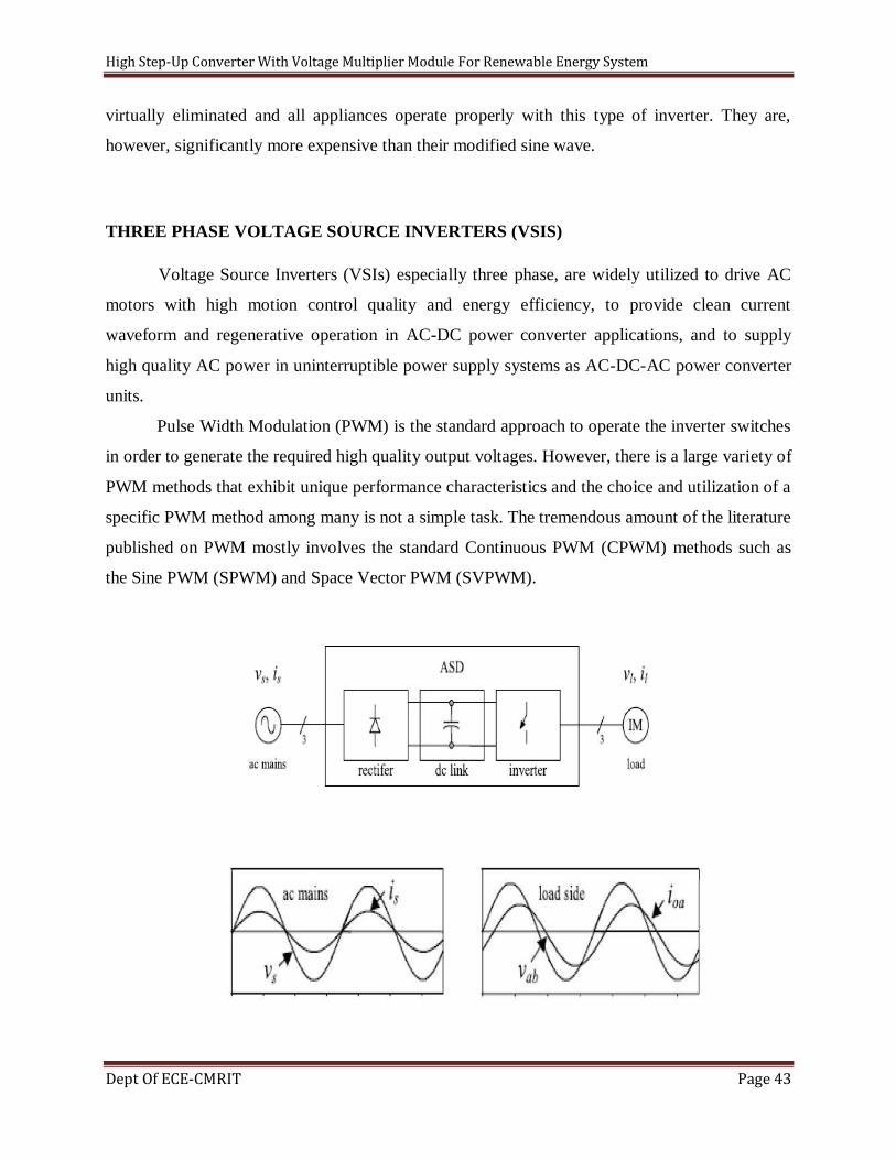
THREE PHASE VOLTAGE SOURCE INVERTERS (VSIS)
Voltage Source Inverters (VSIs) especially three phase, are widely utilized to drive AC
motors with high motion control quality and energy efficiency, to provide clean current
waveform and regenerative operation in AC-DC power converter applications, and to supply
high quality AC power in uninterruptible power supply systems as AC-DC-AC power converter
units.
Pulse Width Modulation (PWM) is the standard approach to operate the inverter switches
in order to generate the required high quality output voltages. However, there is a large variety of
PWM methods that exhibit unique performance characteristics and the choice and utilization of a
specific PWM method among many is not a simple task. The tremendous amount of the literature
published on PWM mostly involves the standard Continuous PWM (CPWM) methods such as
the Sine PWM (SPWM) and Space Vector PWM (SVPWM).
High Step-Up Converter With Voltage Multiplier Module For Renewable Energy System
Dept Of ECE-CMRIT Page 44
The ac output voltage produced by the VSI:
(a) The electrical power conversion topology;
(b) The ideal input (ac mains) and output (load) waveforms; and
(c) The actual input (ac mains) and output (load) waveforms.
The ac output voltage produced by the VSI of a standard Adjustable Speed Drives
(ASDs) can be seen in Figure 2.1. Although this waveform is not sinusoidal as expected (Figure
1(b), its fundamental component behaves as such. This behaviour should be ensured by a
modulating technique that controls the amount of time and the sequence used to switch the
power valves on and off.
Single-phase VSIs cover low-range power applications and three-phase VSIs cover the
medium- to high-power applications. The main purpose of these topologies is to provide a three-
phase voltage source, where the amplitude, phase, and frequency of the voltages should always
be controllable. Although most of the applications require sinusoidal voltage waveforms (e.g.,
ASDs, uninterruptible power supplies and flexible ac transmission systems), arbitrary voltages
are also required in some emerging applications (e.g., active filters, voltage compensators).
The standard three-phase VSI topology is shown in Figure 2.2 and the eight valid switch
states are given in Table 1. As in single-phase VSIs, the switches of any leg of the inverter (S1
and S4, S3 and S6, or S5 and S2) cannot be switched on simultaneously because this would
result in a short circuit across the dc link voltage supply. Similarly, in order to avoid undefined
states in the VSI, and thus undefined ac output line voltages, the switches of any leg of the
inverter cannot be switched off simultaneously as this will result in voltages that will depend
upon the respective line current polarity.
Of the eight valid states, two of them (7 and 8 in Table 2.1) produce zero ac line voltages.
In this case, the ac line currents freewheel through either the upper or lower components. The
remaining states (1 to 6 in Table 2.1) produce non-zero ac output voltages. In order to generate a
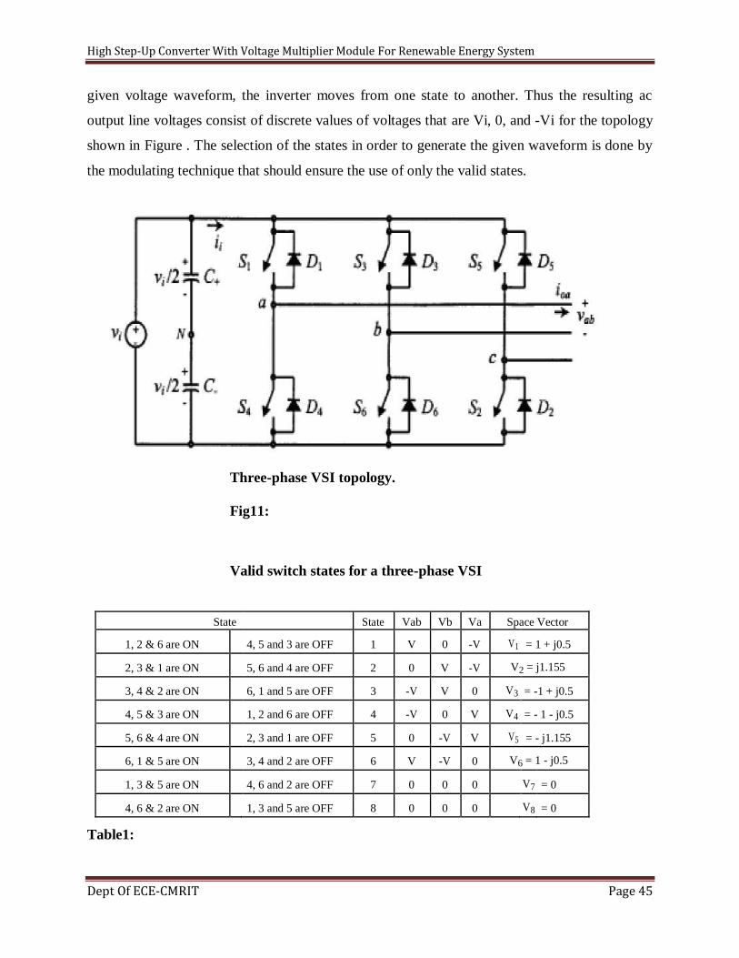
High Step-Up Converter With Voltage Multiplier Module For Renewable Energy System
Dept Of ECE-CMRIT Page 45
given voltage waveform, the inverter moves from one state to another. Thus the resulting ac
output line voltages consist of discrete values of voltages that are Vi, 0, and -Vi for the topology
shown in Figure . The selection of the states in order to generate the given waveform is done by
the modulating technique that should ensure the use of only the valid states.
Three-phase VSI topology.
Fig11:
Valid switch states for a three-phase VSI
State State Vab Vb Va Space Vector
1, 2 & 6 are ON 4, 5 and 3 are OFF 1 V 0 -V V1 = 1 + j0.5
2, 3 & 1 are ON 5, 6 and 4 are OFF 2 0 V -V V2 = j1.155
3, 4 & 2 are ON 6, 1 and 5 are OFF 3 -V V 0 V3 = -1 + j0.5
4, 5 & 3 are ON 1, 2 and 6 are OFF 4 -V 0 V V4 = - 1 - j0.5
5, 6 & 4 are ON 2, 3 and 1 are OFF 5 0 -V V V5 = - j1.155
6, 1 & 5 are ON 3, 4 and 2 are OFF 6 V -V 0 V6 = 1 - j0.5
1, 3 & 5 are ON 4, 6 and 2 are OFF 7 0 0 0 V7 = 0
4, 6 & 2 are ON 1, 3 and 5 are OFF 8 0 0 0 V8 = 0
Table1:
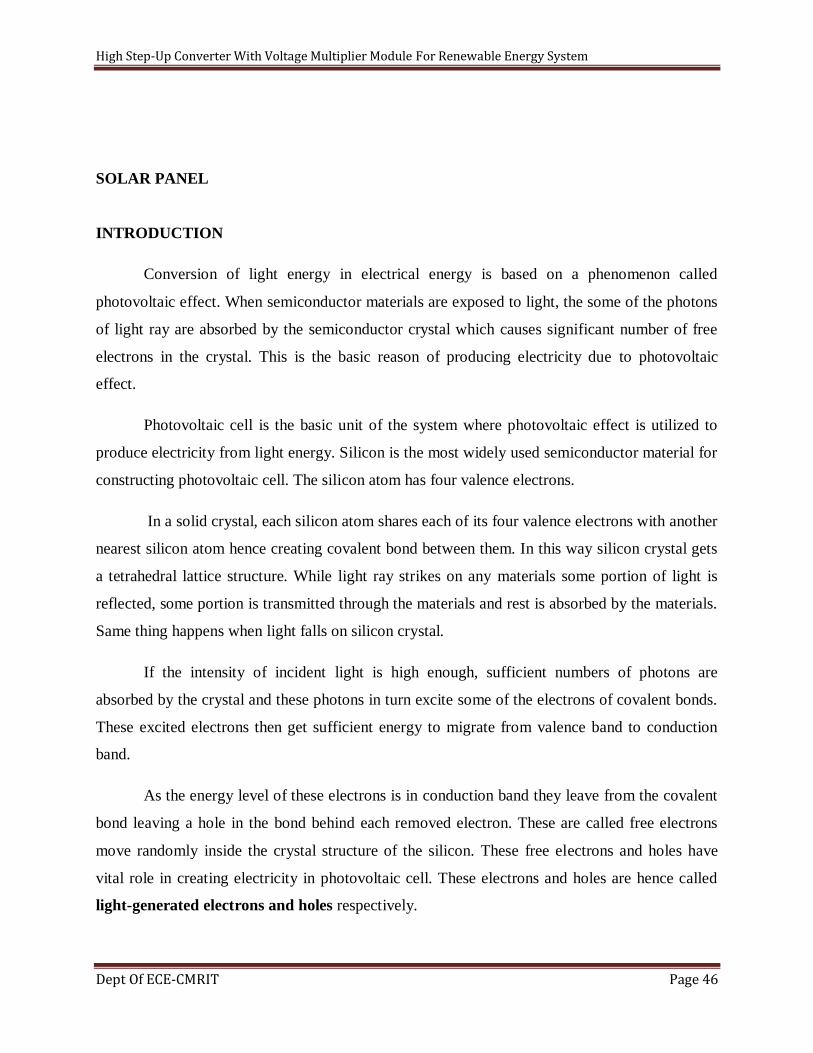
High Step-Up Converter With Voltage Multiplier Module For Renewable Energy System
Dept Of ECE-CMRIT Page 46
SOLAR PANEL
INTRODUCTION
Conversion of light energy in electrical energy is based on a phenomenon called
photovoltaic effect. When semiconductor materials are exposed to light, the some of the photons
of light ray are absorbed by the semiconductor crystal which causes significant number of free
electrons in the crystal. This is the basic reason of producing electricity due to photovoltaic
effect.
Photovoltaic cell is the basic unit of the system where photovoltaic effect is utilized to
produce electricity from light energy. Silicon is the most widely used semiconductor material for
constructing photovoltaic cell. The silicon atom has four valence electrons.
In a solid crystal, each silicon atom shares each of its four valence electrons with another
nearest silicon atom hence creating covalent bond between them. In this way silicon crystal gets
a tetrahedral lattice structure. While light ray strikes on any materials some portion of light is
reflected, some portion is transmitted through the materials and rest is absorbed by the materials.
Same thing happens when light falls on silicon crystal.
If the intensity of incident light is high enough, sufficient numbers of photons are
absorbed by the crystal and these photons in turn excite some of the electrons of covalent bonds.
These excited electrons then get sufficient energy to migrate from valence band to conduction
band.
As the energy level of these electrons is in conduction band they leave from the covalent
bond leaving a hole in the bond behind each removed electron. These are called free electrons
move randomly inside the crystal structure of the silicon. These free electrons and holes have
vital role in creating electricity in photovoltaic cell. These electrons and holes are hence called
light-generated electrons and holes respectively.

High Step-Up Converter With Voltage Multiplier Module For Renewable Energy System
Dept Of ECE-CMRIT Page 47
WORKING PRINCIPLE OF PHOTOVOLTAIC CELL OR SOLAR CELL
When instead pentavalent phosphorous atoms, trivalent impurity atoms like boron are
added to a semiconductor crystal totally opposite type of semiconductor will be created. In this
case some silicon atoms in the crystal lattice will be replaced by boron atoms in other words the
boron atoms will occupy the positions of replaced silicon atoms in lattice structure.
Three valance electrons of boron atom will pair with valance electron of three neighbour
silicon atoms to create three complete covalent bonds. For this configuration there will be a
silicon atom for each boron atom, fourth valance electron of which will not find any neighbour
valance electrons to complete its fourth covalent bond. Hence this fourth valance electron of
these silicon atoms remains unpaired and behaves as incomplete bond.
In a trivalent impurity doped semiconductor a significant number of covalent bonds are
continually broken to complete other incomplete covalent bond. When one bond is broken one
hole is created in it. When one bond in completed, the hole in it disappears. In this way one hole
appears to disappear another neighbour hole. As such holes are having relative motion inside the
semiconductor crystal.
In the view of that it can said that holes also can move freely as free electrons inside
semiconductor crystal. As each of the holes can accept electron, the trivalent impurities are
known as acceptor do pants and the semiconductors doped with acceptor decants are known as p-
type or positive type semiconductor. In n-type semiconductor mainly the free electrons carry
negative charge and in p-type semiconductor mainly the holes in turn carry positive charge
therefore free electrons in n-type semiconductor and free holes in p-type semiconductor are
called majority carrier in n-type semiconductor and p-type semiconductor respectively.
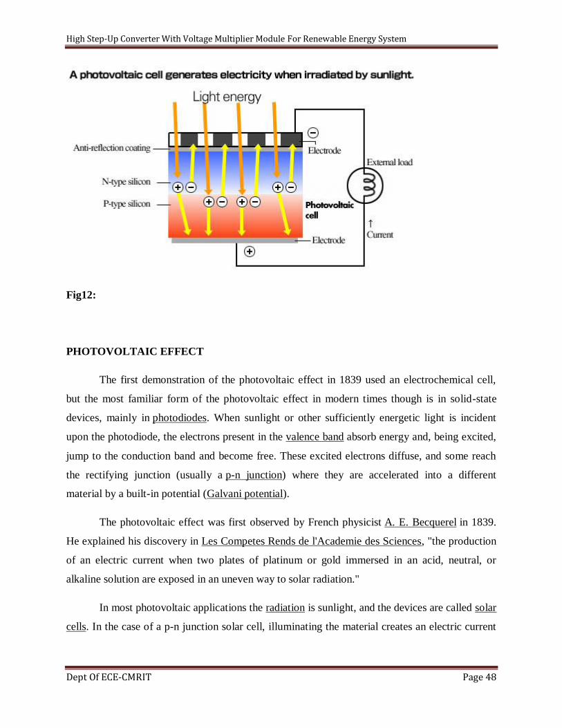
High Step-Up Converter With Voltage Multiplier Module For Renewable Energy System
Dept Of ECE-CMRIT Page 48
Fig12:
PHOTOVOLTAIC EFFECT
The first demonstration of the photovoltaic effect in 1839 used an electrochemical cell,
but the most familiar form of the photovoltaic effect in modern times though is in solid-state
devices, mainly in photodiodes. When sunlight or other sufficiently energetic light is incident
upon the photodiode, the electrons present in the valence band absorb energy and, being excited,
jump to the conduction band and become free. These excited electrons diffuse, and some reach
the rectifying junction (usually a p-n junction) where they are accelerated into a different
material by a built-in potential (Galvani potential).
The photovoltaic effect was first observed by French physicist A. E. Becquerel in 1839.
He explained his discovery in Les Competes Rends de l'Academie des Sciences, "the production
of an electric current when two plates of platinum or gold immersed in an acid, neutral, or
alkaline solution are exposed in an uneven way to solar radiation."
In most photovoltaic applications the radiation is sunlight, and the devices are called solar
cells. In the case of a p-n junction solar cell, illuminating the material creates an electric current
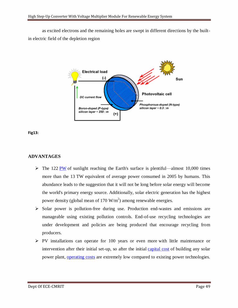
High Step-Up Converter With Voltage Multiplier Module For Renewable Energy System
Dept Of ECE-CMRIT Page 49
as excited electrons and the remaining holes are swept in different directions by the built-
in electric field of the depletion region
Fig13:
ADVANTAGES
The 122 PW of sunlight reaching the Earth's surface is plentiful—almost 10,000 times
more than the 13 TW equivalent of average power consumed in 2005 by humans. This
abundance leads to the suggestion that it will not be long before solar energy will become
the world's primary energy source. Additionally, solar electric generation has the highest
power density (global mean of 170 W/m2) among renewable energies.
Solar power is pollution-free during use. Production end-wastes and emissions are
manageable using existing pollution controls. End-of-use recycling technologies are
under development and policies are being produced that encourage recycling from
producers.
PV installations can operate for 100 years or even more with little maintenance or
intervention after their initial set-up, so after the initial capital cost of building any solar
power plant, operating costs are extremely low compared to existing power technologies.
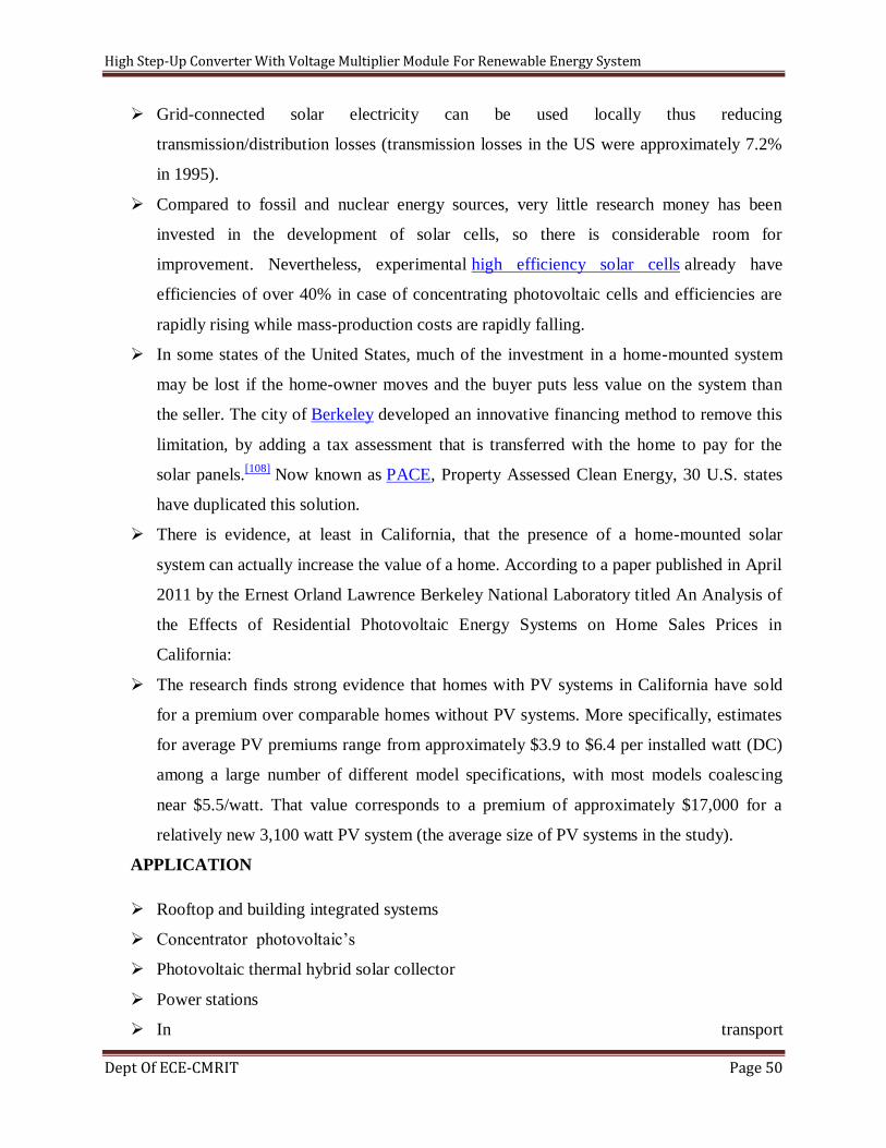
High Step-Up Converter With Voltage Multiplier Module For Renewable Energy System
Dept Of ECE-CMRIT Page 50
Grid-connected solar electricity can be used locally thus reducing
transmission/distribution losses (transmission losses in the US were approximately 7.2%
in 1995).
Compared to fossil and nuclear energy sources, very little research money has been
invested in the development of solar cells, so there is considerable room for
improvement. Nevertheless, experimental high efficiency solar cells already have
efficiencies of over 40% in case of concentrating photovoltaic cells and efficiencies are
rapidly rising while mass-production costs are rapidly falling.
In some states of the United States, much of the investment in a home-mounted system
may be lost if the home-owner moves and the buyer puts less value on the system than
the seller. The city of Berkeley developed an innovative financing method to remove this
limitation, by adding a tax assessment that is transferred with the home to pay for the
solar panels.[108]
Now known as PACE, Property Assessed Clean Energy, 30 U.S. states
have duplicated this solution.
There is evidence, at least in California, that the presence of a home-mounted solar
system can actually increase the value of a home. According to a paper published in April
2011 by the Ernest Orland Lawrence Berkeley National Laboratory titled An Analysis of
the Effects of Residential Photovoltaic Energy Systems on Home Sales Prices in
California:
The research finds strong evidence that homes with PV systems in California have sold
for a premium over comparable homes without PV systems. More specifically, estimates
for average PV premiums range from approximately $3.9 to $6.4 per installed watt (DC)
among a large number of different model specifications, with most models coalescing
near $5.5/watt. That value corresponds to a premium of approximately $17,000 for a
relatively new 3,100 watt PV system (the average size of PV systems in the study).
APPLICATION
Rooftop and building integrated systems
Concentrator photovoltaic’s
Photovoltaic thermal hybrid solar collector
Power stations
In transport
High Step-Up Converter With Voltage Multiplier Module For Renewable Energy System
Dept Of ECE-CMRIT Page 51
Telecommunication and signalling
Spacecraft applications
Specialty Power Systems
PV-PHOTOVOLTAICS
Photovoltaics (PV) is the conversion of light into electricity using semiconducting
materials that exhibit the photovoltaic effect, a phenomenon studied
in physics, photochemistry, and electrochemistry.PV has become the cheapest source of
electrical power in regions with a high potential, with price bids as low as 0.01567
US$/kWh in 2020. Panel prices have dropped by the factor of 10 within a decade. This
competitiveness opens the path to a global transition to sustainable energy which would
be required help to mitigate global warming. The situation is urgent: The emissions
budget for CO
2 to meet the 1.5 degree target would be used up in 2028 if emissions remain on the
current level. However, the use of PV as a main source requires energy storage systems
or global distribution by High-voltage direct current power lines causing additional
costs.A photovoltaic system employs solar modules, each comprising a number of solar
cells, which generate electrical power. PV installations may be ground-mounted, rooftop
mounted, wall mounted or floating. The mount may be fixed or use a solar tracker to
follow the sun across the sky. Solar PV has specific advantages as an energy source: once
installed, its operation generates no pollution and no greenhouse gas emissions, it shows
simple scalability in respect of power needs and silicon has large availability in the
Earth's crust.Photovoltaic systems have long been used in specialized applications as
stand-alone installations and grid-connected PV systems have been in use since the
1990s.
Photovoltaic modules were first mass-produced in 2000, when German
environmentalists and the Eurosolar organization got government funding for a ten
thousand roof program.Advances in technology and increased manufacturing scale have
in any case reduced the cost, increased the reliability, and increased the efficiency of
photovoltaic installations Net metering and financial incentives, such as preferential feed-

High Step-Up Converter With Voltage Multiplier Module For Renewable Energy System
Dept Of ECE-CMRIT Page 52
source in terms of global capacity. The International Energy Agency expects a growth by 700 -
880 GW from 2019 to 2024. According to the forecast, PV could become the technology with
the largest installed capacity by the mid 2020s.In 2018, worldwide installed PV capacity
increased to more than 515 gigawatts (GW) covering approximately two percent of
global electricity demand.With current technology, photovoltaics recoups the energy needed to
manufacture them in 1.5 years in Southern Europe and 2.5 years in Northern Europe.
Photovoltaic (PV) devices generate electricity directly from sunlight via an electronic process
that occurs naturally in certain types of material, called semiconductors. Electrons in these
materials are freed by solar energy and can be induced to travel through an electrical circuit,
powering electrical devices or sending electricity to the grid.PV devices can be used to power
anything from small electronics such as calculators and road signs up to homes and large
commercial businesses.
HOW DOES PV TECHNOLOGY WORK?
Photons strike and ionize semiconductor material on the solar panel, causing outer electrons to
break free of their atomic bonds. Due to the semiconductor structure, the electrons are forced in
one direction creating a flow of electrical current. Solar cells are not 100% efficient in crystalline
silicon solar cells, in part because only certain light within the spectrum can be absorbed. Some
of the light spectrum is reflected, some is too weak to create electricity (infrared) and some
(ultraviolet) creates heat energy instead of electricity.
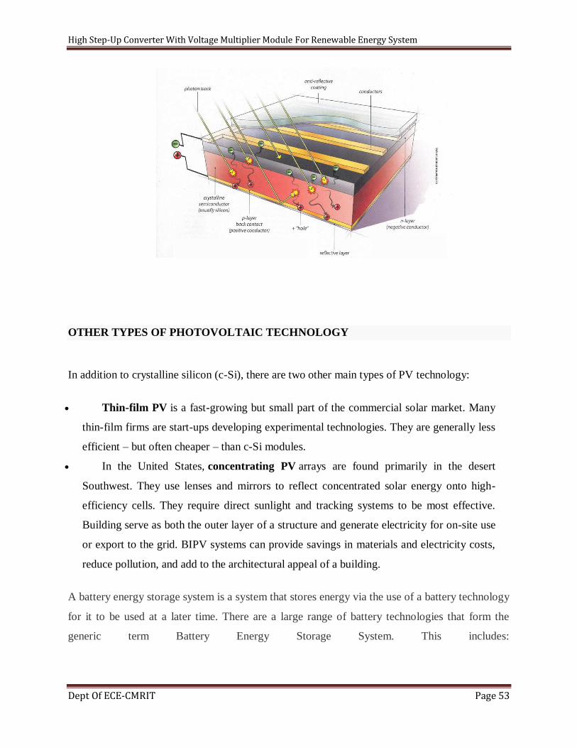
High Step-Up Converter With Voltage Multiplier Module For Renewable Energy System
Dept Of ECE-CMRIT Page 53
OTHER TYPES OF PHOTOVOLTAIC TECHNOLOGY
In addition to crystalline silicon (c-Si), there are two other main types of PV technology:
Thin-film PV is a fast-growing but small part of the commercial solar market. Many
thin-film firms are start-ups developing experimental technologies. They are generally less
efficient – but often cheaper – than c-Si modules.
In the United States, concentrating PV arrays are found primarily in the desert
Southwest. They use lenses and mirrors to reflect concentrated solar energy onto high-
efficiency cells. They require direct sunlight and tracking systems to be most effective.
Building serve as both the outer layer of a structure and generate electricity for on-site use
or export to the grid. BIPV systems can provide savings in materials and electricity costs,
reduce pollution, and add to the architectural appeal of a building.
A battery energy storage system is a system that stores energy via the use of a battery technology
for it to be used at a later time. There are a large range of battery technologies that form the
generic term Battery Energy Storage System. This includes:
High Step-Up Converter With Voltage Multiplier Module For Renewable Energy System
Dept Of ECE-CMRIT Page 54
VRLA or valve regulated lead acid batteries. These are the traditional batteries used in
Uninterruptible Power Supplies and in existence since 1934, their cost is relatively low in
comparison to other battery technologies. Deep cycle VRLA batteries are the type most
suited to energy storage to ensure that they have a long enough life span for this use.
Lithium Ion batteries. This is the type of battery that is commonly found in modern
consumer electronics such as your smartphone. They have a high energy density with the
potential for even higher capacities (lithium ion technology is constantly changing and
improving). The main benefit with lithium ion batteries are that they can be charged and
discharged more often that VRLA batteries with less deterioration in terms of storage
capacity of longevity of product. The main downside is cost although this is coming
down progressively.
Vanadium Flow batteries. This battery uses vanadium ions to store chemical potential
energy. They are currently quite bulky in size but offer the ability to completely
discharge without any adverse effects and a long life time (20+ years).
Sodium Nickel batteries. These batteries use molten salt as the electrolyte. This allows
the batteries to withstand greater temperature extremes as the cells themselves operate at
270+ degrees Celsius and are insulated so that the external chassis is just above ambient
temperature.
Liquid metal batteries. This battery technology uses liquid metals as both the
electrodes and the electrolyte. As there is a constant regeneration between cycles, the
electrodes do not degrade with time. The cost of liquid metal is currently the main
stumbling block.
As well as Battery Energy Storage Systems, there are a number of other energy storage
systems both currently available and under development. This includes:
Compressed air storage – this involves storing air under pressure which can later be
used to spin turbines and produce electricity
Molten salt storage – this involves storing energy as heat rather than a chemical storage
(e.g. battery) or gravitational potential energy (e.g. hydro-electric). Heat is stored within
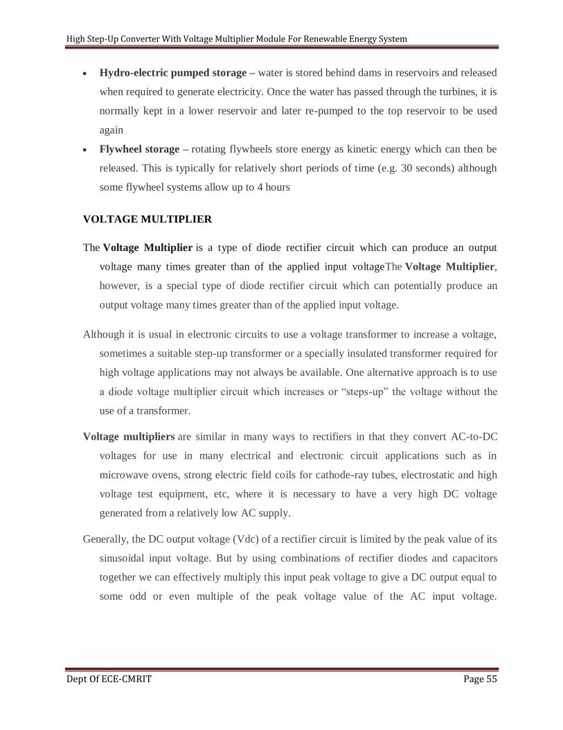
High Step-Up Converter With Voltage Multiplier Module For Renewable Energy System
Dept Of ECE-CMRIT Page 55
Hydro-electric pumped storage – water is stored behind dams in reservoirs and released
when required to generate electricity. Once the water has passed through the turbines, it is
normally kept in a lower reservoir and later re-pumped to the top reservoir to be used
again
Flywheel storage – rotating flywheels store energy as kinetic energy which can then be
released. This is typically for relatively short periods of time (e.g. 30 seconds) although
some flywheel systems allow up to 4 hours
VOLTAGE MULTIPLIER
The Voltage Multiplier is a type of diode rectifier circuit which can produce an output
voltage many times greater than of the applied input voltageThe Voltage Multiplier,
however, is a special type of diode rectifier circuit which can potentially produce an
output voltage many times greater than of the applied input voltage.
Although it is usual in electronic circuits to use a voltage transformer to increase a voltage,
sometimes a suitable step-up transformer or a specially insulated transformer required for
high voltage applications may not always be available. One alternative approach is to use
a diode voltage multiplier circuit which increases or “steps-up” the voltage without the
use of a transformer.
Voltage multipliers are similar in many ways to rectifiers in that they convert AC-to-DC
voltages for use in many electrical and electronic circuit applications such as in
microwave ovens, strong electric field coils for cathode-ray tubes, electrostatic and high
voltage test equipment, etc, where it is necessary to have a very high DC voltage
generated from a relatively low AC supply.
Generally, the DC output voltage (Vdc) of a rectifier circuit is limited by the peak value of its
sinusoidal input voltage. But by using combinations of rectifier diodes and capacitors
together we can effectively multiply this input peak voltage to give a DC output equal to
some odd or even multiple of the peak voltage value of the AC input voltage.
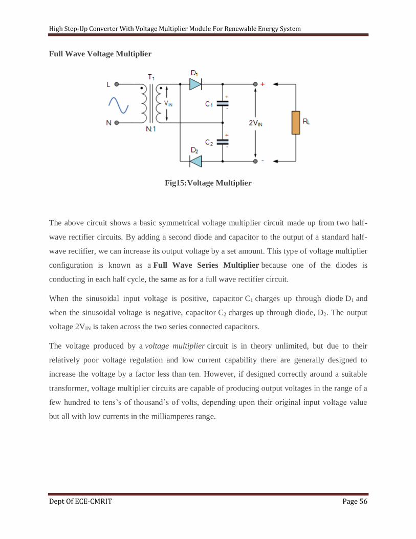
High Step-Up Converter With Voltage Multiplier Module For Renewable Energy System
Dept Of ECE-CMRIT Page 56
Full Wave Voltage Multiplier
Fig15:Voltage Multiplier
The above circuit shows a basic symmetrical voltage multiplier circuit made up from two half-
wave rectifier circuits. By adding a second diode and capacitor to the output of a standard half-
wave rectifier, we can increase its output voltage by a set amount. This type of voltage multiplier
configuration is known as a Full Wave Series Multiplier because one of the diodes is
conducting in each half cycle, the same as for a full wave rectifier circuit.
When the sinusoidal input voltage is positive, capacitor C1 charges up through diode D1 and
when the sinusoidal voltage is negative, capacitor C2 charges up through diode, D2. The output
voltage 2VIN is taken across the two series connected capacitors.
The voltage produced by a voltage multiplier circuit is in theory unlimited, but due to their
relatively poor voltage regulation and low current capability there are generally designed to
increase the voltage by a factor less than ten. However, if designed correctly around a suitable
transformer, voltage multiplier circuits are capable of producing output voltages in the range of a
few hundred to tens’s of thousand’s of volts, depending upon their original input voltage value
but all with low currents in the milliamperes range.
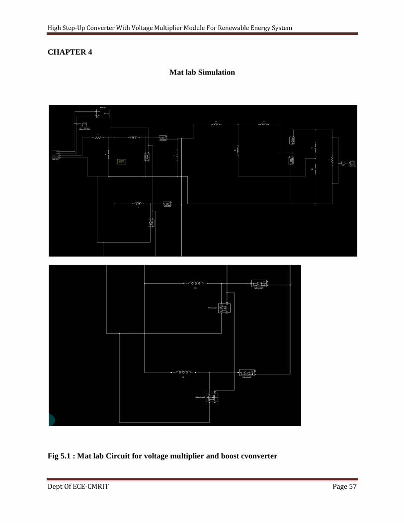
High Step-Up Converter With Voltage Multiplier Module For Renewable Energy System
Dept Of ECE-CMRIT Page 57
CHAPTER 4
Mat lab Simulation
Fig 5.1 : Mat lab Circuit for voltage multiplier and boost cvonverter
High Step-Up Converter With Voltage Multiplier Module For Renewable Energy System
Dept Of ECE-CMRIT Page 58
Fig 5.2 : Solar Cell
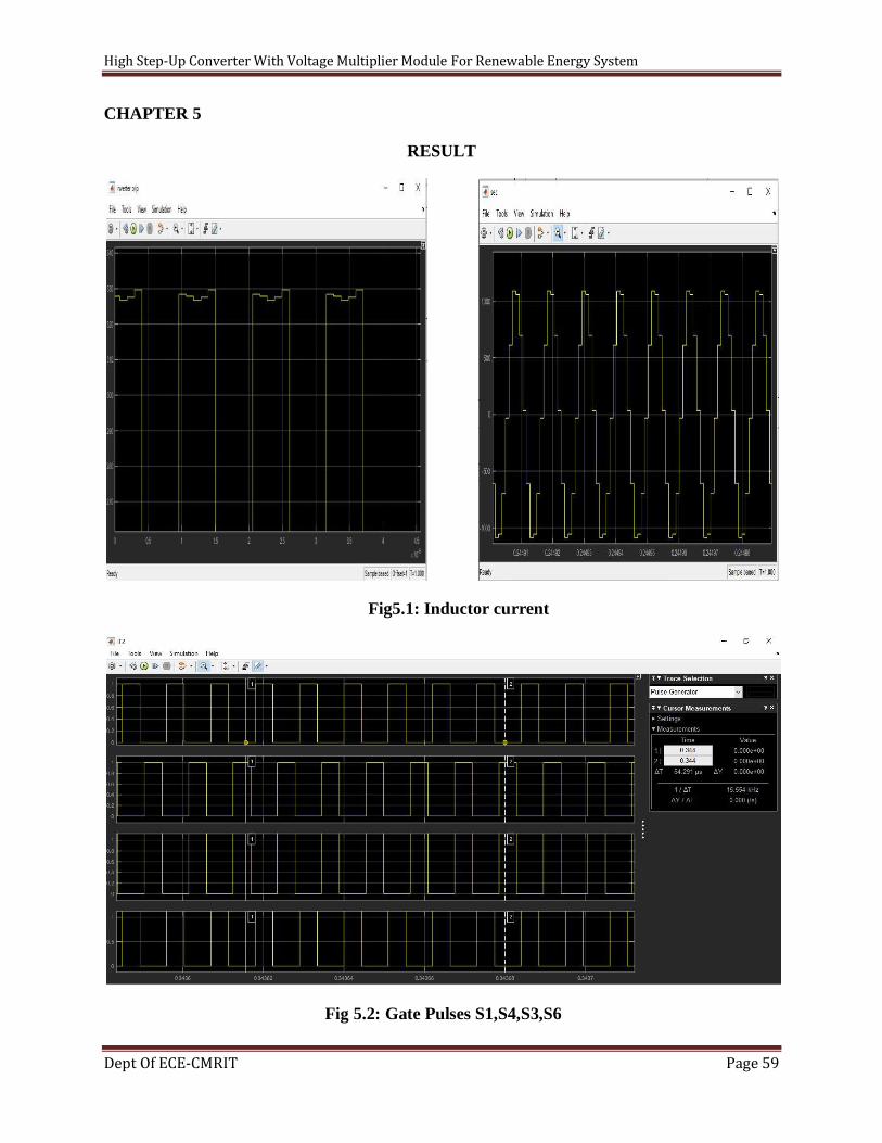
High Step-Up Converter With Voltage Multiplier Module For Renewable Energy System
Dept Of ECE-CMRIT Page 59
CHAPTER 5
RESULT
Fig5.1: Inductor current
Fig 5.2: Gate Pulses S1,S4,S3,S6
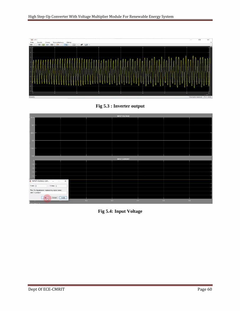
High Step-Up Converter With Voltage Multiplier Module For Renewable Energy System
Dept Of ECE-CMRIT Page 60
Fig 5.3 : Inverter output
Fig 5.4: Input Voltage
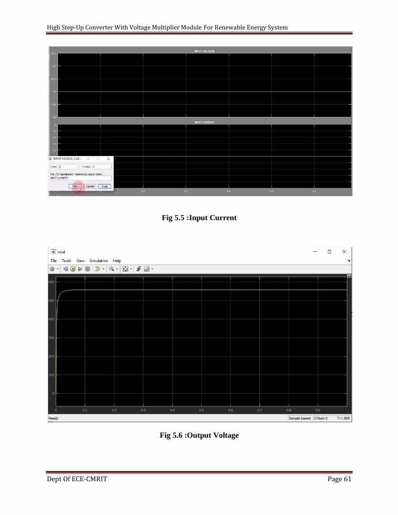
High Step-Up Converter With Voltage Multiplier Module For Renewable Energy System
Dept Of ECE-CMRIT Page 61
Fig 5.5 :Input Current
Fig 5.6 :Output Voltage
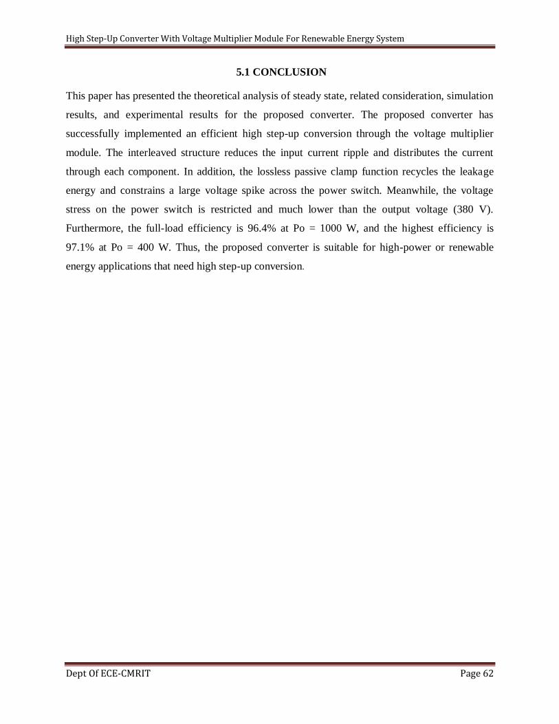
High Step-Up Converter With Voltage Multiplier Module For Renewable Energy System
Dept Of ECE-CMRIT Page 62
5.1 CONCLUSION
This paper has presented the theoretical analysis of steady state, related consideration, simulation
results, and experimental results for the proposed converter. The proposed converter has
successfully implemented an efficient high step-up conversion through the voltage multiplier
module. The interleaved structure reduces the input current ripple and distributes the current
through each component. In addition, the lossless passive clamp function recycles the leakage
energy and constrains a large voltage spike across the power switch. Meanwhile, the voltage
stress on the power switch is restricted and much lower than the output voltage (380 V).
Furthermore, the full-load efficiency is 96.4% at Po = 1000 W, and the highest efficiency is
97.1% at Po = 400 W. Thus, the proposed converter is suitable for high-power or renewable
energy applications that need high step-up conversion.
High Step-Up Converter With Voltage Multiplier Module For Renewable Energy System
Dept Of ECE-CMRIT Page 63
CHAPTER 6
REFERENCE
[1]T. Kefalas and A. Kladas, “Analysis of transformers working under heavily saturated
conditions in grid-connected renewable energy systems,” IEEE Trans. Ind. Electron., vol. 59, no.
5, pp. 2342–2350, May 2012.
[2] J. T. Bialasiewicz, “Renewable energy systems with photovoltaic power generators:
Operation and modeling,” IEEE Trans. Ind. Electron., vol. 55, no. 7, pp. 2752–2758, Jul. 2008.
[3] S. M. Chen, T. J. Liang, L. S. Yang, and J. F. Chen, “A safety enhanced, high step-up DC–
DC converter for AC photovoltaic module application,” IEEE Trans. Power Electron., vol. 27,
no. 4, pp. 1809–1817, Apr. 2012.
[4] Z. Song, C. Xia, and T. Liu, “Predictive current control of three-phase grid-connected
converters with constant switching frequency for wind energy systems,” IEEE Trans. Ind.
Electron., vol. 60, no. 6, pp. 2451–2464, Jun. 2013.
[5] L. Barote, C. Marinescu, and M. N. Cirstea, “Control structure for single-phase stand-alone
wind-based energy sources,” IEEE Trans. Ind. Electron., vol. 60, no. 2, pp. 764–772, Feb. 2013.
[6] Y.-P. Hsieh, J.-F. Chen, T.-J. Liang, and L. S. Yang, “A novel high step-up DC–DC
converter for a microgrid system,” IEEE Trans. Power Electron., vol. 26, no. 4, pp. 1127–1136,
Apr. 2011.
[7] C. T. Pan and C. M. Lai, “A high-efficiency high step-up converter with low switch voltage
stress for fuel-cell system applications,” IEEE Trans. Ind. Electron., vol. 57, no. 6, pp. 1998–
2006, Jun. 2010.