Embed Size (px)
Citation preview

Project Number: ECE-PCP - 0801
POWER SUPPLY FOR MRI ENVIRONMENT
A Major Qualifying Project Report:
submitted to the Faculty
of the
WORCESTER POLYTECHNIC INSTITUTE
in partial fulfillment of the requirements for the
Degree of Bachelor of Science
by
Bernard J. Lis III
Date: April 30, 2009
Approved:
Professor Peder C. Pedersen, Major Advisor
This report represents the work of one or more WPI undergraduate students
submitted to the faculty as evidence of completion of a degree requirement.
WPI routinely publishes these reports on its web site without editorial or peer review.
I
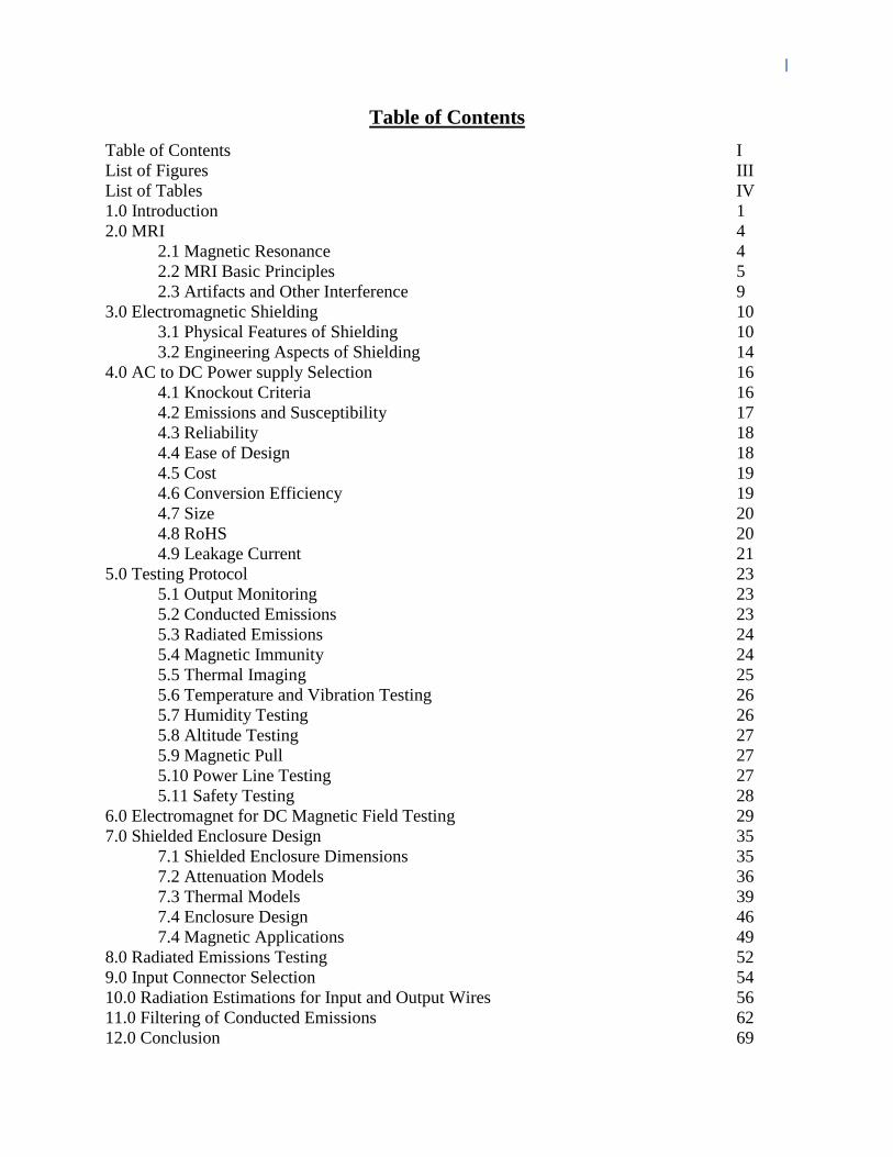
Table of Contents
Table of Contents I
List of Figures III
List of Tables IV
1.0 Introduction 1
2.0 MRI 4
2.1 Magnetic Resonance 4
2.2 MRI Basic Principles 5
2.3 Artifacts and Other Interference 9
3.0 Electromagnetic Shielding 10
3.1 Physical Features of Shielding 10
3.2 Engineering Aspects of Shielding 14
4.0 AC to DC Power supply Selection 16
4.1 Knockout Criteria 16
4.2 Emissions and Susceptibility 17
4.3 Reliability 18
4.4 Ease of Design 18
4.5 Cost 19
4.6 Conversion Efficiency 19
4.7 Size 20
4.8 RoHS 20
4.9 Leakage Current 21
5.0 Testing Protocol 23
5.1 Output Monitoring 23
5.2 Conducted Emissions 23
5.3 Radiated Emissions 24
5.4 Magnetic Immunity 24
5.5 Thermal Imaging 25
5.6 Temperature and Vibration Testing 26
5.7 Humidity Testing 26
5.8 Altitude Testing 27
5.9 Magnetic Pull 27
5.10 Power Line Testing 27
5.11 Safety Testing 28
6.0 Electromagnet for DC Magnetic Field Testing 29
7.0 Shielded Enclosure Design 35
7.1 Shielded Enclosure Dimensions 35
7.2 Attenuation Models 36
7.3 Thermal Models 39
7.4 Enclosure Design 46
7.4 Magnetic Applications 49
8.0 Radiated Emissions Testing 52
9.0 Input Connector Selection 54
10.0 Radiation Estimations for Input and Output Wires 56
11.0 Filtering of Conducted Emissions 62
12.0 Conclusion 69

II
Sources 71
Appendix A 72
III
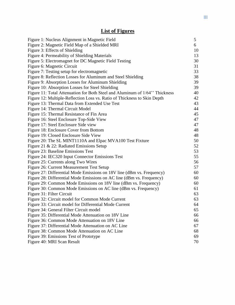
List of Figures
Figure 1: Nucleus Alignment in Magnetic Field 5
Figure 2: Magnetic Field Map of a Shielded MRI 6
Figure 3: Effects of Shielding 10
Figure 4: Permeability of Shielding Materials 13
Figure 5: Electromagnet for DC Magnetic Field Testing 30
Figure 6: Magnetic Circuit 31
Figure 7: Testing setup for electromagnetic 33
Figure 8: Reflection Losses for Aluminum and Steel Shielding 38
Figure 9: Absorption Losses for Aluminum Shielding 39
Figure 10: Absorption Losses for Steel Shielding 39
Figure 11: Total Attenuation for Both Steel and Aluminum of 1/64’’ Thickness 40
Figure 12: Multiple-Reflection Loss vs. Ratio of Thickness to Skin Depth 42
Figure 13: Thermal Data from Extended Use Test 43
Figure 14: Thermal Circuit Model 44
Figure 15: Thermal Resistance of Fin Area 45
Figure 16: Steel Enclosure Top-Side View 47
Figure 17: Steel Enclosure Side view 47
Figure 18: Enclosure Cover from Bottom 48
Figure 19: Closed Enclosure Side View 48
Figure 20: The SL MINT1110A and Elpac MVA100 Test Fixture 50
Figure 21 & 22: Radiated Emissions Setup 52
Figure 23: Baseline Emissions Test 53
Figure 24: IEC320 Input Connector Emissions Test 55
Figure 25: Currents along Two Wires 56
Figure 26: Current Measurement Test Setup 57
Figure 27: Differential Mode Emissions on 18V line (dBm vs. Frequency) 60
Figure 28: Differential Mode Emissions on AC line (dBm vs. Frequency) 60
Figure 29: Common Mode Emissions on 18V line (dBm vs. Frequency) 60
Figure 30: Common Mode Emissions on AC line (dBm vs. Frequency) 61
Figure 31: Filter Circuit 63
Figure 32: Circuit model for Common Mode Current 63
Figure 33: Circuit model for Differential Mode Current 64
Figure 34: General Filter Circuit model 65
Figure 35: Differential Mode Attenuation on 18V Line 66
Figure 36: Common Mode Attenuation on 18V Line 66
Figure 37: Differential Mode Attenuation on AC Line 67
Figure 38: Common Mode Attenuation on AC Line 68
Figure 39: Emissions Test of Prototype 69
Figure 40: MRI Scan Result 70

IV
List of Tables
Table 1: Nuclei and Their Gyromagnetic Ratio 8
Table 2: Properties of Shielding Materials at 150 kHz 12
Table 3: AC to DC Power supply Efficiency 19
Table 4: Decision Matrix 21
Table 5: Magnetic Field with Varying Current, 1’’ Gap 31
Table 6: 60 Amps through Coils, Magnetic Field 32
Table 7: Results of Magnetic Susceptibility Test 51
Table 8: Current Measurements with 18 Watt Resistor 54
Table 8: Current Measurements with 90 Watt Resistor 54
Table 9: Current Measurements with Open Output 55
Table 10: Current Measurements with Patient Monitor 55
Table 11: Filter Component Values and Derating 62

V

1
1.0 Introduction
Magnetic Resonance Imaging (MRI) has become an important diagnostic tool, because it
is a noninvasive way to diagnose almost any person at any age. In 2003, 10,000 MRI units were
in existence worldwide. This number increased to 26,503 MRI units in 2008 (Hornak, 2008).
About 75 million MRI scans are performed every year (Hornak, 2008). Using magnetic fields,
MRI can create images of the human brain, spine, and nearly every other part of the human body.
This can eliminate the need for exploratory surgery. MR can also help diagnosis many health
related issues such as carotid artery disease, screen for intracranial aneurysms, and screen for
renal artery stenosis.
An MRI room is a harsh electromagnetic (EM) environment for electronics. Sometimes a
patient monitor is needed to monitor the patient’s physiological status. Monitoring takes place
when a patient is unable to alert health care providers about pain, cardiac problems, or
respiratory problems. This patient monitor needs to be designed to function correctly within the
constraints of the EM environment. Shielding can enclose electronic devices in order to attenuate
the strength of magnetic fields to a level at which the device can survive. Without proper
shielding, the magnetic fields produced by the MRI scans might damage electronics as well as
pull ferromagnetic objects into the bore of the MRI. Conversely, interference from electronics
has the potential for causing false images to be obtained from the MRI. For these reasons and
more, there are special patient monitoring systems that are designed to work within an MRI
environment.
Philips provides one such patient monitoring system. This product can monitor a patient’s
blood pressure, blood oxygen level, respiration, and much more. It is designed to survive the
MRI environment and not affect imaging. Patient vital signs are taken by a base unit that is a
minimum of one foot away from the MRI magnet. In the observation room, a wireless monitor
displays all readings.
Currently, power supplies in the MRI environment have limited functionality according
how closely they can be placed near the MRI unit. This is due to the magnetic field that is
present, which causes some power supplies to fail. An object with ferromagnetic material will be
pulled into the MRI machine, and become attached to the MRI magnet. In order to prevent power

2
supplies from being drawn into the MRI machine, Velcro strips are commonly used to keep
power supplies attached to the floor. A long, shielded cable is used to connect the power supply
to the patient monitor it powers. This approach goes against two key features of an MR patient
monitor. Cost needs to be kept to a minimum, but the shielded cable is expensive. Mobility is
also needed, and the range of the patient monitor is limited by the shielded cable it is attached to.
Ideally, the power supply should be attached to the patient monitoring unit. This would lower the
cost of the shielded cable that connects the power supply to the patient monitor, because it can be
shorter. The mobility of the patient monitor will also be increased, because the power supply is
not attached to a fixed point.
An AC to DC power supply suitable for an MRI compatible patient monitor will be the
focus of this MQP project. This power supply will address the shortcomings of the current design
mentioned above. The Philips patient monitor requires an AC to DC power supply that converts
a worldwide line input of 100, 120, 220, or 240 Volts AC at 50 Hz or 60 Hz to an 18 Volt, 5
Amp DC output. The resources behind designing a power supply board can be extensive. A great
deal of testing needs to be performed. A custom power supply would need be produced relatively
quickly for completion of the project, and may not be at the same quality of a off the shelf power
supply, which has had years of resources given to it. Any power supply would also have to
comply with safety regulations regarding patient monitoring systems, such as IEC60601.
Because such a power supply would have already gone through the regulation process, it would
just need to be qualified for the purposes of this project.
This project will require research into the basic principles of MRI in order to understand
what to expect from the environment. This will be useful to help predict noise on the power line,
the strength and frequency of electromagnetic interference produced by these power lines, and
unacceptable interference that can be produced by the power supply. Research in
electromagnetic compatibility, shielding techniques, and filtering will help decide what designs
will be considered to protect the AC to DC power supply from the MRI environment. This will
require the selection of a off the shelf power supply. Test procedures will be researched and
created in order to test design options. Also, a test procedure that can emulate an MRI would be
helpful so that scheduling field tests with a hospital will be minimized. Research and/or

3
consultation will also be needed to create the casing and shielding for the power supply. Both of
these tasks will require some mechanical design to create.
The deliverables that will come from this project are as follows:
Research into shielding techniques
Research into testing which could emulate an MRI room. This is important so that
hospital field tests can be kept to a minimum. In general, hospital tests are hard to
schedule, and provide small windows in which to test designs
Provide a prototype for a new power supply which can supply 18 Volts DC at 5
Amps to an MRI compatible patient monitor. This power supply will need to
survive the MRI environment, and not interfere with the MRI imaging process

4
2.0 MRI
This section will discuss some of the principles in magnetic resonance imaging (MRI).
The focus of this section will be the magnetic fields and radiofrequency pulses which make the
MRI environment a challenge for electronics design.
2.1 Magnetic Resonance
To understand the concepts behind the MRI, magnetic resonance (MR) first needs to be
understood. MR is a concept based on the spin of an atom’s nucleus. This spin occurs naturally,
and creates a magnetic field parallel to the axis of rotation. There are a select group of elements,
which have a net spin and therefore can be detected in MRI. These elements include 1H,
2H,
31P,
23Na,
14N,
13C, and
19F. Without the presence of a magnetic field, any volume of tissue contains
a collection of nuclei with random orientation. The seven nuclei mentioned above will produce
magnetic fields created by their spin. The direction of the magnetic field of each of these nuclei
will depend on the random orientation of that nucleus’s axis of rotation. The magnetic field of
each nucleus is of equal magnitude. However, a vector addition of a very large number of these
magnetic fields will produce a net magnetization of approximately zero in the volume of tissue.
When placed in a magnetic field (B0), the specified nuclei will align slightly away from
the direction of the magnetic field at an angle (θ) (Haacke et al, 1999). However, these nuclei
will not remain in this orientation. Instead, they will have an axis of rotation parallel to the
magnetic field. For a better understanding of how this works, refer to Figure 1. The magnetic
field (B0) is directed along the z axis. The vector μ shows the orientation of the nucleus’ axis.
The nucleus will rotate in this orientation around the z axis at a frequency ω0, which is called the
Larmor frequency. This frequency is dependent on the strength of the field and on the specific
molecule being imaged (water, fat, etc) (Haacke et al, 1999). The angle dΦ is the phase
difference as the nucleus rotates at the Larmor frequency. This is relative the angle at which the
nucleus begins its rotation. Because each nucleus is randomly oriented away from the z axis, the
net magnetization perpendicular to the magnetic field is zero. However, because each nucleus is
spinning around the z axis over time, the net magnetization will not be zero. When there is no
magnetic field present, the nuclei no longer are oriented about the z axis, and instead return again
to their random orientation in the volume of tissue.

5
Figure 1: Nucleus Alignment in Magnetic Field (Haacke et al, 1999)
Magnetic resonance is a process of absorption and reemission of energy. Atoms will be
subjected to a magnetic field, resulting in a fraction of the protons aligning with the magnetic
field. At this point, the atoms will be in a low energy state. To get to a high energy state, the
atoms will absorb photons. This energy is defined in eq. (1) (Hornak, 2008).
E = h ω0 (1)
where h is Plank’s constant (6.626x10⁻³⁴
J s), E is energy, and ω0 is the Larmor frequency. The
atom will absorb some of this energy at the Larmor frequency, and then reemit this energy at the
same frequency. The atom will then return to the original low energy state, and reemit the energy
it absorbed. It is this reemitted energy that can be captured and observed. A loop of wire is used
to induce a voltage from the emitted energy of each nucleus. This induced voltage, which is
called the free induction decay, will decay over time as the atoms emit their absorbed energy and
return to their original state (Brown and Semelka, 1999). The free induction decay consists of
many frequencies superimposed onto each other. From these frequencies, images can be created.
2.2 MRI Basic Principles
Magnetic Resonance Imaging (MRI) uses the concepts of magnetic resonance with some
additional concepts of its own. The first principle of MRI is the DC magnetic field to orient the

6
nuclei with atomic spin. Some clinical MRI systems can achieve up to 10 Tesla, but typically up
to 3 or 4 Tesla MRI machines are used. The strength of static magnetic fields use in MRI is
increasing with new generations of MRI machines, because the signal to noise ratio increases
linearly with the strength of the magnetic field. This is because there is larger percentage of
nuclei aligned with the magnetic field as the magnitude of the magnetic field increases. To keep
magnetic field levels outside the MRI bore at a constant level, higher magnetic fields in MRIs
lead to the need for shielding. Usually, shielding in accomplished through additional coils.
Figure 2 shows a magnetic field map of a shielded MRI.
Figure 2: Magnetic Field Map of a Shielded MRI (Overweg, 2006)
The purpose of the shielded MRI is to attenuate the magnetic fields leaving the MRI for
safety purposes. With the typical shielded magnet seen above, the magnetic field outside of the
MRI is proportional to 1/r5 (Overweg, 2006). There will be a significant drop off when moving
away from the magnet. However, the magnetic fields seen in the MRI environment are strong
enough, even with a significant drop off, to damage electronics and pull magnetic objects.

7
An additional concept important to MRI is the use of gradient fields that create
differences in the magnetic field. Gradient fields are generated by current flowing through
individual loops of wire mounted together into a single gradient coil. These gradient fields cause
rapid changes in the magnetic field that can be in the kilohertz range or smaller, depending on
the speed of the gradient. When the gradient is introduced, the Larmor frequency of the atoms in
a body that were once uniform in the presence of the magnetic field will vary with location due
to the gradient field. Each location now corresponds to a different frequency, and these
frequency differences become a kind of coordinate system.
It is important to understand what frequency values the Larmor frequencies can take on,
because these will be the frequencies that can’t be interfered with by the patient monitor power
supply. Different molecules of the body will have different Larmor frequencies if subjected to
the same magnetic field. This is dependent on the gyromagnetic ratio (γ) (Brown and Semelka,
1999). Water and fat are examples of nuclei that experience different Larmor frequencies. The
magnitude of the magnetic field applied to an atom will also affect the Larmor frequency. Eq (2)
gives an understanding of the impact of the gyromagnetic ratio (Hornak, 2008).
ω0 = 2 π γ B0 eq (2)
Images are created of these different molecules by recognizing the frequency at the location that
was scanned. In order to obtain the MR signal as a function of frequency instead of time, a
Fourier transformation is used. This information is then processed, and an image is created. This
project is not too concerned with the imaging process. This project is concerned with the levels
of interference between the MRI and power supply.
The patient is subjected to pulses of radiofrequency energy. The purpose of these
radiofrequency pulses is to change the orientation of a selected grouping of atoms to the high
energy state. This high energy state is called the anti-parallel state. In this state, atoms are tilted
at an angle of 90° with respect to the magnetic field. As shown by eq (1), the radiofrequency
energy will be a pulse at the Larmor frequency in order to excite the atom. Remember that the
Larmor frequency is proportional to the magnetic field. Because the magnetic field has a linear
change due to the gradient field, Larmor frequencies will be different at each location (Brown
and Semelka, 1999). This means that the range of frequencies for the radio frequency energy can

8
be selected so that only desired sections of the body are tilted into the anti-parallels state. This is
useful when MRIs are only needed of select areas, such as the brain or heart. Frequencies
corresponding to those areas will be used. Without a radio frequency pulse to enter the high
energy state, atoms are oriented along the magnetic field.
The radio frequency energy applied in MRI is usually a uniform magnitude of excitation
among a range of frequencies with some center frequency. The bandwidth of the radio frequency
energy will allow for selected regions of tissue to be excited. For this project, it is important to
know the frequencies of these pulses, because it will play a part in interference issues. These
frequencies are dependent on the nuclei and magnetic field intensity. This dependence is
represented by the gyromagnetic ratio. Table 1 contains a list of each nucleus that has a net spin
along with their gyromagnetic ratio.
Table 1: Nuclei and Their Gyromagnetic Ratio (Hornak, 2008)
Static magnetic fields seen from an MRI can be as low as 0.2 Tesla and exceed 4 Tesla. The
element predominately used in MRI is the proton in the 1H hydrogen atom (Brown and Semelka,
1999). Using eq (1) and the values for the static magnetic field and gyromagnetic ratio, the
Larmor frequencies might reach as low as 3 MHz (0.2 Tesla) and exceed 170 MHz (4 Tesla) for
1H. If MRIs reach as high as 8 Tesla, which is the current limit for adults, children, and infants
above the age of one month (Hornak, 2008), Larmor frequencies as high as 425 MHz may be
seen for 1H. This is a wide range of frequencies that must not be interfered with.
9
When the radio frequency energy is no longer introduced, every atom will return to their
origin orientation. Frequency and phase maps are created of each atom by the unique magnetic
field located at each point (Brown and Semelka, 1999). These maps are what create MRI images.
2.3 Artifacts and Other Interference
MRI images are susceptible to image artifacts. Artifacts are pixels in an MRI image that
do not accurately represent the anatomy being shown. An important aspect of this project is to
ensure that no artifacts will be created by the power supply being designed. Sources of artifacts
include the physical motion of the patient, limitations in measurement process, and external
sources. This project’s concern is with the external source, which would be the patient monitor
power supply. One source of artifacts is time varying signals detected by the receiver. Artifacts
from this source will appear as lines of constant frequency in the image. The largest concern of
interference will be emissions in the range of the RF pulses used by the MRI. Any interference
from devices on these frequencies will be received by the receiver coil, and cause errors in MRI
images. As stated above, these can will RF pulses can range from 8.5 MHz to 170 MHz.
However, as the strength of magnetic fields increase this range will increase.
The increasing strength in the MRI magnetic field also poses a concern to the power
supply. Interference with the static magnetic field and gradient field will not be of concern,
because the power supply will not be able to produce any magnetic field close to the scale of the
MRI. Instead, the interference onto the power supply by the MRI is a concern. Ferromagnetic
materials in electronics components such as inductors and transformers can saturate under the
magnetic field. This saturation will cause large increases in current that can damage the power
supply itself. The patient monitor power supply may therefore have to be shielded from the
magnetic fields present from an MRI, as well as shield the MRI from emissions in the range
specified that originates from the power supply.

10
3.0 Electromagnetic Shielding
Due to the intense magnetic fields of an MRI, the AC to DC power supply that will be
selected is likely to need some sort of shielding. Also, radiated emission from the AC to DC
power supply and any cabling connected to it may cause artifacts to appear on the MRI image.
Both these issues are related to electromagnetic interference. A solution to electromagnetic
interference applied to an electrical device is to create an electromagnetic shield. This shield will
attenuate electromagnetic interference according to three physical features of transmission losses
introduced by the electromagnetic shielding. These features, which can be seen in Figure 3, are
external reflection, absorption, and internal reflection.
3.1 Physical Features of Shielding
Figure 3: Effects of Shielding (Hemming, 1992)
The first attenuation of a shielding enclosure occurs when the amplitude of an incident
wave is reflected from the surface of the electromagnetic shield. This attenuation is due to the
fact that there is an impedance mismatch between the air to metal boundary. External reflection
loss is dependent on both the surface and wave impedance. It is helpful to think of this as a
transmission line system. The input impedance would be the impedance of the source in air, and
likewise the transmission line impedance would be represented by the surface impedance of the

11
shielding material. A mismatch will introduce a reflection back to the source. The surface
impedance of the electromagnetic shield can be expressed by the eq 3 (Hemming, 1992).
Zs = [ jωμ ( ζ + jωε ) ]1/2
Ω (3)
where Ω, μ, ζ, and ε are resistance, permeability, conductivity and permittivity, respectively.
The surface impedance, Zs, is a function of the source type, which is either an electric or
magnetic field, and the distance from the source to the shield. There are various equations for the
external reflection loss depending on the type of source, which includes magnetic fields, plane-
waves, and electric fields. Plane-waves and electric fields have high impedance, and will have
external reflection losses from the air to metal boundary. This allows for thin shielding. Magnetic
fields have low impedance. For magnetic fields, there will be internal reflection losses from the
metal to air boundary, but external reflection losses will be negligible from the air to metal
boundary. Magnetic fields require thick shielding as well (Barnes, 1987). Reflection losses of
shielding will be important for the interference from the power supply onto the MRI, but not for
shielding the power supply from the magnetic fields present in the MRI. This is because constant
magnetic fields can be diverted, but not reflected. The effectiveness of this feature of shielding
will be diminished by interface connections such as screws, rivets, and welds. Bowing or
waviness to the shielding will cause slits or gaps which will allow for leakage. It is important to
make sure that the shielded enclosure is as close to a homogeneous wall or material as possible.
Energy that is not reflected is then absorbed by passing through the shielding. In a
transmission line system, this would be the losses incurred while the wave propagates along the
transmission line. This absorption loss can be expressed in the following equation (Hemming,
1992).
A = 1.314[(ω ∙ μr ∙ ζr /(2π)] ½ ∙ d (4)
where d, μr, and ζr are shield thickness, relative permeability to air, and relative conductivity to
copper.
It is important to realize that the relative permeability will not remain constant for all
frequencies. Shielding materials will have specific frequency ranges in which they are more
effective due to its relative permeability. Below is a table of the electrical properties of shielding

12
materials at 150 kilohertz, as well as a graph displaying the relative permeability of shielding
materials at low frequencies. Mumetal and permalloy have a relative permeability of over 10,000
at low frequencies, and are still an effective shielding material at higher frequencies. In fact, they
are more effective material than most other shielding materials for magnetic fields at both low
and high frequencies. These look to be the most likely candidates for shielding. Absorption will
be more effective for the RF pulses present in an MRI environment than for the magnetic fields
present. The absorption of low frequency magnetic fields will require more thickness. This is
evident when looking at eq 4.
Table 2: Properties of Shielding Materials at 150 kHz (Hemming, 1992)

13
Figure 4: Permeability of Shielding Materials (Haacke et al, 1999)
One of the difficulties in shielding design is that the ferromagnetic materials should not
be saturated; otherwise they will lose their ability to attenuate the magnetic field. One solution to
this is to create a double-layered shield. The outer layer will have a low relative permeability and
low susceptibility to saturation. This will reduce the incident magnetic field and allow the second
shield to work properly (Paul, 2006).
Just as the incident wave hitting the surface of the shielding was reflected, any remaining
incident wave inside the shielding will be attenuated by the internal reflection losses introduced
by the second metal to air boundary. In a transmission line system, this internal reflection loss
would be similar to the reflection loses due to a mismatch of impedances between the
transmission line and the load. For most cases, only the initial reflection losses and absorption
losses need to be calculated. This second reflection loss is usually negligible. This is especially
the case for most materials when shielding against waves in the Megahertz range (Hemming,
1992). However, as mentioned before, this will be a factor of transmission loss for low frequency
magnetic fields.

14
3.2 Engineering Aspects of Shielding
There are some rules of thumb in shielding for safety margins. These safety margins are
additional attenuation loss above the minimum requirement for interference on the power supply
from the MRI as well as on the MRI from the power supply. In general, shielding should provide
at least 20 dB of attenuation above the required attenuation levels at frequencies above 10 MHz.
Shielding should also provide at least 10 dB above requirement at 10 MHz, and 6 dB above
requirement below 100 kHz (Hemming, 1992). Of all these frequency ranges, low frequency
magnetic shielding is the most difficult shielding to achieve. Using these safety margins will
ensure that interference is at an acceptable level. For this project’s applications, there are two
areas of concern. The first is low frequency magnetic fields. The static magnetic field and
gradient field may affect ferromagnetic devices such as transformers and inductors in the power
supply. These ferromagnetic devices may reach their saturation points. This will cause large
currents in the device that may damage the power supply. The second area of concern is
interference from the power supply in the order of Megahertz. This may come from the device
output, the switching frequency, or some other high frequency source within the device.
All the losses that were described rely on the fact that a continuous layer of shielding
material is used to attenuate fields. When a layer of shielding is not continuous, the shielding
loses effectiveness, as fields are now allowed to penetrate the shielding without being attenuate
as the shield was designed. Penetration of the electromagnetic shield is the biggest challenge for
shielding design. Seams are one area of concern. The most reliable shielding seam is welded.
However, it is expensive because there must be a minimum thickness, which is usually 16 gauge
or higher (Hemming, 1992). This type of seam has the best performance. Seams can also be
clamped. If there is not a continuous metal to metal seal, then this can provide a source of
leakage. Plane wave shielding is usually the most difficult for this type of seam, because plane
waves will cause the most leakage. A sandwich seam uses waveguide-beyond cutoff principle for
RF seals. Unlike other seaming approaches, it does not rely on continuous metal to metal seals.
This is good for high frequency performance, because this is where the reliance on continuous
metal to metal seals can cause issues. Copper tape can also be used. However, it does not allow
for highly effective shielding above 60 dB.

15
A requirement of shielded enclosures is that all external connection to the inside of the
shielding enclosure must be filtered. This is due to the interference on wiring outside of the
shielded enclosure. The most common filters used for shielded enclosures are reflective filters,
which are combinations of capacitors and inductors mounted inside a sealed metal can. It is
important to note that any inductors used in filtering must be non-ferrous core. This is due to the
fact that any ferromagnetic materials used for inductors could be saturated due to the magnetic
fields present in an MRI environment. Reflective filters, made for low sources and impedances,
most commonly use a T shaped combination of inductors and capacitors, while those made for
high sources and impedances most commonly use a pi shaped combination (Hemming, 1992).
Low pass filters are the most common filter for electromagnetic compatibility. Filters are
characterized by their attenuation at given frequencies, impedance levels, voltage ratings, current
rating, size, weight, temperature, and reliability. The filtering mentioned above will be a concern
for the AC line input to the power supply. The largest concern is the noise on top of the AC
power signal. This would most likely be due to the RF pulses of the MRI. The output to the
patient monitor will also be of concern. Again, any high frequency interference in the Megahertz
range cannot emanate from the output line. In order to prevent this, shielded wire will be needed.
16
4.0 AC to DC Power Supply Selection
The first step of designing proper shielding and filtering for a patient monitor power
supply is to select a capable AC to DC power supply. The selection process will need to be an
objective weighting of various aspects of the AC to DC power supplies that are important to take
into account. These aspects will be referred to as decision factors. This process of deciding the
best available AC to DC power supply will use a matrix for a visual aid. This matrix will list all
the decision factors considered for selecting an AC to DC power supply. These decision factors
were determined in discussion with Paul Bailey, who is the Philip’s project manager. Each
decision factor will be weighted on a scale of 0 to 100, with 100 being the most important. To
relate each AC to DC power supply to another, grades will be assigned to each AC to DC power
supply for each decision factor. Each AC to DC power supply will be graded on a scale of 0 to
10 for each decision factor. Grades will be multiplied by the decision factor it corresponds to.
Then, totals will be added to determine the best AC to DC power supply. There are four AC to
DC power supplies that will be evaluated. These are the Elpac MVA100, the Emerson LPS174-
M, the SL MINT1110A, and the Tectrol 1402. All of these AC to DC power supplies have data
sheets available in the Appendix, except for the Tectrol 1402. The data that was used to relate the
Tectrol 1402 to the other power supplies is part of a Philips report. This report was not included
in this document.
4.1 Knockout Criteria
A must for each AC to DC power supply is 90 Watts of output power. The AC to DC
power supply will provide 18 Volts at 5 Amps. If a power supply cannot supply this in some
form, it will not be considered for this application. This will be considered knockout criteria.
This decision factor is weighted at 100, as it is a must. The Elpac, Emerson, and SL AC to DC
power supplies all provide this amount of power. They are all graded at 10. The Tectrol 1402
however only supplies 35 Watts of power. However, three 1402s can be combined in parallel for
the power needed. For this reason, the Tectrol 1402 was given a 5.
There are two other factors that are knockout criteria. The first is that these AC to DC
power supplies must fulfill medical standards such as UL/IEC 60601-1-2 and CSA 22.2, because
they are powering patient monitoring equipment. The other is that these supplies must have

17
universal inputs. This means that they must be able to operate with power outlets anywhere in
the world. These decision factors are weighted at 100, because all AC to DC power supplys must
fulfill these conditions. All supplies meet these conditions, and receive a 10 for a grade.
4.2 Emissions and Magnetic Field Susceptibility
These factors are radiated emissions, conducted emissions, output noise, and magnetic
field susceptibility. A 3 Tesla MRI machine will be one of the more predominant environments
the power supply will face. However, MRI machines are now reaching levels of 5 Tesla, and
levels will increase further in the future. Emissions in the Megahertz range will be unwanted,
because this will interfere with the MRI at the Larmor frequencies. These factors will determine
what needs to be shielded or filtered later in the design process. The less emissions or magnetic
susceptibility will mean that less shielding will be required. This may save money, and simplify
design. These design factors were given a weight of 80.
The first consideration is magnetic field susceptibility. The Tectrol 1402 was tested with
a real MRI and survived. It was given a 10 for susceptibility. The SL and Elpac supplies were
tested using an electromagnetic to simulate the MRI. The SL supply passed. However, it did not
survive in a true MRI environment, so it was only given an 8. The Elpac supply did fail to
operate once after increasing the magnetic field significantly in an instant. However, this was a
onetime incident that could not be replicated. It passed otherwise. It was therefore given a 7. The
Emerson supply was not tested, because it was eliminated from consideration early in the
decision making process.
Emissions testing was also completed on all supplies. Two types of emission test were
performed. The first, radiated emissions testing, used an antenna to measure emissions from the
power supply. The second, conducted emissions testing, monitored noise on the AC power cable.
With the exception of the Tectrol 1402, supplies were tested at 90 Watts and 18 Watts. The
Tectrol 1402 cannot supply 90 Watts unless connected together with others. For this reason,
emissions are expected to be additive when 90 Watts is needed. The Astec supply did not
perform well, and was given a 1 accordingly. The SL and Elpac supplies both performed well,
and were very close. Each was given a 9. The Tectrol 1402 performed well at low power, but

18
again it is expected to perform worse when multiple supplies are connected. It is unsure what this
will result it. It was therefore given a 5.
4.3 Reliability
Reliability is an important aspect of this design. An operating temperature range of 10°C
to 40°C is the minimal requirement. A storage temperature range of -15°C to 50°C is the
minimal requirement. If a supply cannot operate at the maximum temperature range, additional
cooling solutions are needed. This will only complicate the design. A humidity rating of 80% is
also needed. These are general reliability requirements. Because of the emphasis on reliability,
this decision factor was given a weight of 90. The Tectrol 1402 is used with many Philips
products, and has reportedly performed well. However, one concern was noticed while reading
its datasheet. Beyond 35°C, power will linearly decline to 25W at 55°C. This could be a concern
because the power supply will only be able to dissipate heat through the casing. The 1402 was
given a reliability grade of 9, because it is used is many reliable Philips products. The Emerson
and SL power supplies were given a grade of 6, because of their high operating ranges for
temperature and humidity. However, very little information is known otherwise. The Elpac
power supply has lower operating ranges, so it received a grade of 5. Again, little will be known
about these other supplies until they are tested for performance with the final design.
4.4 Ease of Design
Ease of design is another factor that should be taken into consideration. Ease of design is
the ease at which an AC to DC power supply can be integrated into an enclosure and conduct
thermally. AC to DC power supplies that have ways to attach to an outside cover will make
mechanical design easier. If the AC to DC power supply also includes a thermal contact to
dissipate heat it will also help to keep the unit within the desired temperature range. These design
factors were given a weight of 70. The Emerson supply offers space for thermal contacts, and is
able to be mounted with its current casing. However, Emerson offers very little customization if
modifications are needed. It received a grade of 7. The SL power supply offers much of the
same, except that modifications can be made to the unit. It received a grade of 10. The Elpac
power supply is small and offers little room for thermal contacts, and dissipates most heat
through metal contacts of the side of the unit. It received a grade of 5. The 1402 will include a

19
cover that can dissipate heat, and heat sinks can easily be added. The 1402 can also be easily
held inside the shielded enclosure. For this reason, the 1402 was given a grade of 9.
4.5 Cost
There are other design characteristics which are easier to explain, such as cost. This was
weighted with a 70. However, quality is the most desired characteristic. Therefore, cost can be
sacrificed for important performance related decision factors. Three Tectrol 1402s will be
needed. However, these will be about two thirds of the cost of the Emerson power supply. Both
the Elpac and SL power supplies are close in price, which is about two thirds the price of three
Tectrol 1402s. The Elpac and SL supplies were given 10s. The Tectrol 1402 was given a 7. The
Emerson power supply was given a 4.
4.6 Conversion Efficiency
Conversion efficiency is an important decision factor for many reasons. The better the
efficiency, the less power is wasted. This will also reduce the heat generated in the device. This
decision factor was given a weight of 80, because it serves as an important part of other factors.
A test was performed to determine the efficiencies of each AC to DC power supply. Two
international AC line extremes of 270 Volts AC at 66 Hertz and 88 Volts AC at 47 Hertz were
used. The results of this test are shown in Table 3. The Elpac power supply was given a 10 due to
it being the best. The SL power supply was given a grade of 7, as it performed lower than the
Elpac power supply. Both the Emerson and Tectrol 1402 performed poorly. They were both
given a 3.
Table 3: AC to DC Power supply Efficiency
Power
Supply
Input
Voltage
(V)
Input
Frequency
(Hz)
Load
Current
(A)
Power
In (W)
Power Out
(W)
Efficiency
(%)
Emerson 270 66 5 116 90 77.586
Emerson 270 66 1 35 18 51.428
Emerson 88 47 5 118 90 76.271
Emerson 88 47 1 35.1 18 51.282
SL 270 66 5 106.1 90 84.825
SL 270 66 1 25.3 18 71.146
SL 88 47 5 108.7 90 82.796
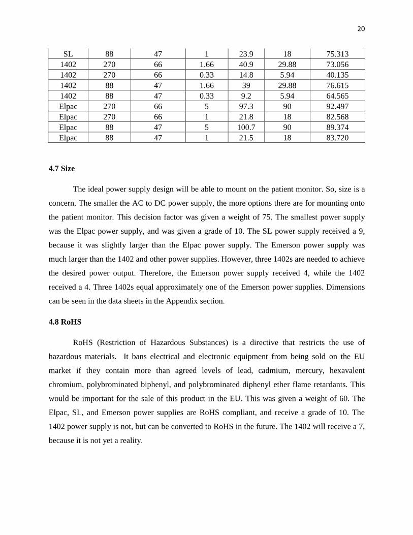
20
SL 88 47 1 23.9 18 75.313
1402 270 66 1.66 40.9 29.88 73.056
1402 270 66 0.33 14.8 5.94 40.135
1402 88 47 1.66 39 29.88 76.615
1402 88 47 0.33 9.2 5.94 64.565
Elpac 270 66 5 97.3 90 92.497
Elpac 270 66 1 21.8 18 82.568
Elpac 88 47 5 100.7 90 89.374
Elpac 88 47 1 21.5 18 83.720
4.7 Size
The ideal power supply design will be able to mount on the patient monitor. So, size is a
concern. The smaller the AC to DC power supply, the more options there are for mounting onto
the patient monitor. This decision factor was given a weight of 75. The smallest power supply
was the Elpac power supply, and was given a grade of 10. The SL power supply received a 9,
because it was slightly larger than the Elpac power supply. The Emerson power supply was
much larger than the 1402 and other power supplies. However, three 1402s are needed to achieve
the desired power output. Therefore, the Emerson power supply received 4, while the 1402
received a 4. Three 1402s equal approximately one of the Emerson power supplies. Dimensions
can be seen in the data sheets in the Appendix section.
4.8 RoHS
RoHS (Restriction of Hazardous Substances) is a directive that restricts the use of
hazardous materials. It bans electrical and electronic equipment from being sold on the EU
market if they contain more than agreed levels of lead, cadmium, mercury, hexavalent
chromium, polybrominated biphenyl, and polybrominated diphenyl ether flame retardants. This
would be important for the sale of this product in the EU. This was given a weight of 60. The
Elpac, SL, and Emerson power supplies are RoHS compliant, and receive a grade of 10. The
1402 power supply is not, but can be converted to RoHS in the future. The 1402 will receive a 7,
because it is not yet a reality.

21
4.9 Leakage Current
Limitations on leakage current are due to the risk of shock from touching the casing. IEC
60601 is a standard that only allows for 500μA of leakage current. A power supply with less
leakage current provides more leeway when designing external filters. This was given a weight
of 65. The SL power supply has a leakage current of less than 50μA, and was given a 10 due to it
being the best. The Emerson power supply has a leakage current of less than 100μA, and was
given a grade of 7. The Elpac power supply has a leakage current of less than 100μA normally,
but can possibly reach 200μA in international applications. It was given a grade of 5. The 1402
power supply has a leakage current of less than 500μA with the multiple supplies needed to
reach 90 Watts of power. Therefore, it was given a grade of 1.
Table 4: Decision Matrix
Decision Factor Weight Elpac
MVA100
Emerson
NSF110
SL
MINT1110A
Tectrol 1402
18V @ 5A 100 10 10 10 5
Medical Standard 100 10 10 10 10
Universal Input 100 10 10 10 10
Magnetic
Susceptibility
80 7 NA 8 10
Emissions 80 9 1 9 5
Reliability 90 5 6 6 9
Ease of Design 70 5 7 10 9
Cost 70 10 4 10 7
Efficiency 80 10 3 7 3
Size 80 10 4 9 2
RoHS 60 10 10 10 7
Leakage Current 65 5 7 10 1
Total 8555 6225* 9180 7015
* Magnetic Immunity not performed, so rating is incomplete
Without any testing, it looks as though the SL and Elpac power supplies are the best
candidates for the MRI power supply. The SL MINT1110A appears to be the better supply of the

22
two, and will be the first choice for this project’s applications. However, testing for emissions,
susceptibility, and reliability will be important in ensuring each power supply’s ability to fill the
project’s needs. Even though each power supply has been tested by its manufacturer, it is
important to ensure that it will survive the environmental conditions the power supply will face.
Table 4 shows the grades, weights, and totals determined in this decision process.

23
5.0 Testing Protocol
There are many concerns for a power supply design for an MRI environment. Most of
those concerns deal with radiated emissions and magnetic susceptibility. The first three tests
described in this section will focus on emissions from the power supply. The fourth test
described in this section will focus on the MRIs effects on the power supply. All the other tests
in this section are for reliability purposes. Because the power supply is powering a patient
monitor, reliability testing will be very important. All testing will be done with the SL
MINT1110A as well as the Elpac MVA100. After the initial testing with the AC to DC power
supplies, the prototype power supply will be tested. The finished product will then have to go
through addition testing to be sold to hospitals.
5.1 Output Monitoring
Purpose: To measure frequencies which make up the DC output of the power supply. If the
power supply output contains noise at the Larmor frequency range, then there will be a
possibility of interference with the MRI imaging. Filtering the output and shielding the output
cable would be two ways to eliminate the noise.
Procedure: Using an oscilloscope and spectrum analyzer, the frequencies of the power supply
output will be measured. Two different electrical loads will be used at different operating
extremes. These loads will draw the current extremes, which are 1 and 5 Amps, a typical load
range of patient monitors. Two different AC operating extremes of 88 Volts AC at 47 Hertz and
270 Volts AC at 66 Hertz will be used.
5.2 Conducted Emissions
Purpose: To measure frequencies which make up the AC input of the power supply. If the power
supply input contains noise at the Larmor frequency range, then there will be a possibility of
interference with the MRI imaging. Unfortunately, the AC input cable will be a standard, non-
shielded IEC320 cable. Filtering may reduce this noise.
Procedure: Using a spectrum analyzer, the frequencies of the power supply output will be
measured. Two different electrical loads will be used at different operating extremes. These
loads will draw the current extremes, which are 1 and 5 Amps, a typical load range of patient

24
monitors. Two different AC operating extremes of 88 Volts AC at 47 Hertz and 270 Volts AC at
66 Hertz will be used.
5.3 Radiated Emissions
Purpose: To determine RF emissions from the power supply. Any emissions in the Larmor
frequency can be received by the MRI, and cause artifacts in the imaging process. A shielded
enclosure will be created to prevent this interference.
Procedure: After a finished prototype is made, screening will be performed in a Philips test
room. This room is a small, shielded enclosure that will screen for the various Larmor
frequencies that can interfere with the MRI. The project prototype will be powering a 3160 unit.
This 3160 unit is a Philips Healthcare/Invivo brand patient monitor that is compatible for the
MRI environment. The 3160 unit will be place in its designated area in the chamber. The power
supply will be placed next to the 3160 unit. Each measurement made at a specific frequency will
have its own emissions limit. The Mr. Fusion prototype must be 5 dB below the limit at each
frequency. The 5 dB will be a safety margin to ensure that the power supply will not interfere
with MRI imaging. At least ten tests will be carried out. Multiple tests will provide multiple
measurements, and provide some idea if there are any spikes that may occur over time. This will
be the last test for radiated emissions before testing the final product in an MRI environment.
Once in an MRI environment, any radiated emissions will appear as constant lines in the MRI
image. This will determine whether or not the power supply is interfering with the MRI. The first
MRI testing will be performed at the Philips’ complex at Gainesville, Florida. If the product
passes all testing at Gainesville, three MRI facilities will be used for testing.
5.4 Magnetic Immunity
Purpose: The static magnetic field of the MRI will be the greatest concern, as well as the
gradient fields around the 1-100 kHz range. Components with ferromagnetic material in the
power supply can be pushed into their saturation points by the large magnetic field. This will
cause a surge in current that may not be protected. This surge may destroy other components,
and therefore destroy the power supply itself. Therefore, testing needs to be done to determine
what magnetic field levels will cause the power supply to fail in operation.

25
Procedure: First, a general screening will be made at the Philips test center. A DC magnetic field
is needed for complete testing. In order to accomplish this, a DC magnet was made. This magnet
was created by looping 8 gauge wire around a C clamp made of iron and steel. The shielded
enclosure will be placed in the gap of the core. This gap can be adjusted to the enclosure’s size.
The magnet is discussed in section 6. A gauss meter will be used to measure the field both
outside and inside the shielded enclosure, against one of the walls. The output of the power
supply will be measured, as well as the temperatures at transformers and other areas of the power
supply. Data will be collected using a data logger. This will give an idea for the attenuation the
shielded enclosure provides. Only relative measurements can be provided by this test. An AC
power supply can also be used to test gradient field levels. Therefore, this electromagnetic will
only be able to serve as the initial magnetic immunity test.
When a finished product is created, an MRI environment will be used to measure
magnetic susceptibility as well. The power supply will start away from the MRI, and gradually
be moved toward the MRI. The power supply will move along an axis that is oriented
horizontally alone the center of the MRI. During testing, a gauss meter will show the strength of
the magnetic field at each point. Different orientations will be used at each point as well.
Measurements will be made at the output of the power supply to ensure that it is operating as it
should. Temperature measurements at points on the power supply will also be measured. This
will determine if the power supply is being interference with by the MRI.
5.5 Thermal Imaging
Purpose: Because the AC to DC power supply will be enclosed, air will not be able to move
through the unit. The main source of heat dissipation will be through the walls of the shielded
enclosure. In order to keep components below their temperature limits, heat sinks may need to be
added. Thermal Imaging will help determine whether this is the case.
Procedure: Thermal mapping is a collection of images and data taken of the power supply while
it is operating. The power supply will be under the maximum load condition of 5 Amps. This is
to ensure that the unit is dissipating maximum heat. Images were taken during using an infrared
camera. Images will give approximate temperature readings. The areas with the greatest
temperature, or hot spots, will be identified. These hot spots will then be tested through the use

26
of thermocouples. Thermocouples can be connected to a data logging device, and the
temperature can be more accurately measured.
5.6 Temperature and Vibration Testing
Purpose: For reliability purposes, the power supply will be ran at the extremes for temperature it
will face while in operation and storage. Vibration will also ensure that the product is not
damage during movement. This is important, as the patient monitor is mobile. This is to ensure
that the product will remain functional during use.
Procedure: The power supply will be place in a test chamber, which will cycle through various
temperatures. The chamber will change to temperature extremes, and then dwell for 3 hours. The
high operating temperatures will be 40°C, 45°C, and 50°C. The low operating temperatures will
be 10°C, 5°C, and 0°C. Storage temperatures of -20°C and 70°C will be tested as well. The dwell
time for these temperatures will be closer to 10 hours. After successful testing, the temperature
will be cycled from 50°C to 0°C. The chamber will stay at either temperature for a 2 hour dwell
period, and then change to the other temperature. Meanwhile, the power supply will be cycled
through various input conditions. Two different AC operating extremes of 88 Volts AC at 47
Hertz and 270 Volts AC at 66 Hertz will be used. The power supply will also go through on and
off cycles. If this is successful, vibration will be added to the beginning of each 2 hour dwell.
During this testing, the output of the power supply will be monitored and logged. This will allow
for the test to be run without the need of an observer. All information of device misbehavior will
be saved and time stamped.
5.7 Humidity Testing
Purpose: For reliability purposes, the power supply will be run at the humidity extremes that it
will face while in operation and storage. This is to ensure that the product will remain functional
during use.
Procedure: Using another test chamber, the power supply will be tested in humidity. The power
supply will spend one day in the chamber under conditions of 45ºC and 95% humidity while
operating. It will then spend a day in the chamber under conditions of 60ºC and 85% humidity
for storage. Finally, the power supply will spend another day in the chamber under conditions of

27
45ºC and 95% humidity while operating. During the testing, the output of the power supply will
be monitored and logged.
5.8 Altitude Testing
Purpose: For reliability purposes, the power supply will be ran at the extremes for altitude it will
face while in operation and storage. This is to ensure that the product will remain functional
during use.
Procedure: Using another test chamber, the power supply will be tested in humidity. The power
supply will spend one day in the chamber under conditions of -10ºC at 9900ft without power. It
will then spend a day in the chamber under conditions of 50ºC at 9900ft while operating. Finally,
the power supply will spend another day in the chamber under conditions of 10ºC at 9900ft while
operating while operating. During the testing, the output of the power supply will be monitored
and logged.
5.9 Magnetic Pull
Purpose: Because of the intense magnetic fields present in MRIs, metallic objects will be pulled
towards the magnetic. The power supply will be subject to pull from the MRI’s magnetic field
when placed on the ground. In order to ensure that the power supply is safe and will not harm
both the patient and the MRI, magnetic pull tests need to be performed.
Procedure: The power supply will be subject to a DC magnetic field. The power supply will be
attached to a meter which can measure the force exerted on the power supply by the magnetic
field. The power supply should not be pulled with a force more than a tenth of its weight. If the
power supply is pulled by a force less than a tenth of its weight, then gravity will ensure that the
power supply is not pulled into the MRI magnet. Measurements will be made both with the
magnet made for magnetic testing as well as at the Gainesville complex.
5.10 Power Line Testing
Purpose: Voltage spikes and drop outs will occur on the AC line. Hospital power often is subject
to these conditions. In fact, it is often the most common place for these occurrences. Therefore,
the power supply must be tested under these conditions to ensure that it will not fail.
28
Procedure: The AC line of the power supply will be placed into an AC power generator. This
generator is capable of creating the surge and power dropout conditions such as brownout and
blackout that will occur. The power supply will be connected to an oscilloscope. Unlike the
reliability tests, the AC line tests are fast. Data logging will not be able to see any problems that
occur, unless the power supply is permanently damage. For this reason, the oscilloscope will be
used to monitor the power supply output.
5.11 Safety Testing
Purpose: Two tests fall under safety testing. The first is leakage current testing. The Mr. Fusions
power supply cannot have a leakage higher than 500 μA according to safety regulations. This is
to protect any users from receiving a substantial shock. The second test is ESD testing. This is to
ensure that a user cannot harm the power supply from the buildup of static shock.
Procedure: For leakage current testing, the power supply is placed into a unit that measures the
leakage current. The power supply will be powering the 3160 unit. As for ESD testing, the power
supply will be shocked with 8 kV spikes. This will simulate human static shock. The output of
the power supply will be monitored to ensure that ESD will not affect operation.

29
6.0 Electromagnet for DC Magnetic Field Testing
One aspect of this project is to protect the power supply from magnetic fields that would
otherwise cause the device to deviate from its desired performance. It is not practical to use a
real MRI for initial testing, due to limited availability. Therefore, either a permanent magnet or
an electromagnet can be used to emulate the MRI environment. The benefit of an electromagnet
is the ability to control the magnetic field. The field can be turned on or off. When turned on,
varying current in the electromagnet’s coils will allow for variable magnetic fields. The
electromagnetic will be used to measure both power supply susceptibility to magnetic fields and
the effectiveness of magnetic shielding.
Figure 5 shows the test setup used for DC magnetic field testing. A C-clamp was used as
the electromagnet’s core, which coils are wrapped around. These coils will create a magnetic
field directed through their center. The C-clamp is a combination of steel and iron, which are
both materials with a high permeability. The magnetic field is directed across a gap of the C-
clamp. Directing the field across a gap allows for a concentrated field. Because the C-clamp gap
can be varied, the magnetic field can be increased by shortening the gap as much as possible.
Also, the magnetic field will decrease rapidly moving away from the gap. This limits the safety
issues present in the lab area. Another safety issue with the electromagnet was presented by the
large amounts of current through the coils. The wire used for the coils was rated for temperatures
up to 90 °C. After a certain period of time (depending on the magnitude of the current), the coils
would reach their maximum rated temperature. To extend this period of time, a fan was used to
cool the electromagnet. The temperature of the electromagnet was measured with an infrared
temperature sensor as well as thermocouple wire. The thermocouples were attached to a data
logger, which made graphing the temperature over time possible.

30
Figure 5: Electromagnet for DC Magnetic Field Testing. A fan is used to cool the coils. The
power supply to the right is driving the current of the coils.
As stated, the magnetic field can be increased by varying both current and gap size. The
largest DC supply available to this project without purchase could provide up to 105 Amps. The
gap size was limited by the size of the device under test. Tables of initial data on the magnet’s
magnetic field can be found on the following page. This data was composed using a DC power
supply that could provide only a maximum of 60 Amps. A 105 Amp supply was used later in
experimentation, because the magnetic field intensity was not strong enough using the 60 Amp
maximum of the previous supply.
Tables 5 and 6 show the field measurements taken for varying current levels and gap
lengths. These field measurements can be estimated using a “magnetic circuit”. The magnetic
circuit uses circuit analysis to show the properties of the electromagnet. The first component of
the magnetic circuit is a voltage source that represents the magnetomotive force. This is equal to
the number of turns multiplied by the current (NI). The other components of the circuit are
resistances that model the steel C-clamp, the adjustable iron bar, and the air gap. The current in
this circuit is the magnetic flux. The magnetic circuit for the electromagnet can be shown in
Figure 6.

31
Figure 6: Magnetic Circuit
The number of turns in the electromagnet is approximately 140. The resistance of each
material is equal to L/(μA), where L is the length, μ is the permeability, and A is the area. Rsteel is
equal to 886 N/(m A2). The other resistances, Riron and Rgap, are dependent on the length of each.
Riron is equal to 981*L N/(m A)2. Rgap is equal to 196*L N/(m A)
2. Obtaining the magnetic flux,
which is simply obtaining the current of the magnetic circuit, will in turn provide the information
for the magnetic field. The equation for magnetic flux is the following
Φ = ∫S B∙dS eq. (1)
where Φ, B, and S are magnetic flux, magnetic field, and surface area. In Tables 5 and 6 are
both the expected and measured magnetic fields.
Table 5: Magnetic Field with Varying Current, 1’’ Gap, measured at left end of gap
Current
(Amps)
Voltage
(Volts)
Resistance
(Ohms)
Power
(Watts)
Measured Magnetic
Field (kilogauss)
Expected Magnetic
Field (kilogauss)
10 0.685 0.0685 6.9 0.225 0.159
20 1.354 0.0677 27.1 0.265 0.318
30 2.054 0.0685 61.6 0.31 0.476
40 2.754 0.0689 110.2 0.35 0.635
50 3.525 0.0705 176.3 0.41 0.794
60 4.205 0.0701 252.3 0.43 0.953

32
Table 6: 60 Amps through Coils, Magnetic Field measured at left end and midpoint of gap
Gap
(inches)
Magnetic Field @ Left End
(kilogauss)
Expected Magnetic Field
(kilogauss)
Magnetic Field @
Midpoint (kilogauss)
2 0.34 0.069 0.175
3 0.32 0.059 0.1
4 0.315 0.052 0.068
5 0.315 0.046 0.055
6 0.31 0.042 0.045
7 0.31 0.038 0.038
From the expected magnetic fields, it looks as though the electromagnet is not performing
as well as expected in Table 5 when current was increased. However, increasing the gap did not
have as great an effect as expected, as Table 6 shows. In this case, the electromagnet
outperformed expectations. There may be some variation in the measurements, but these are
interesting results. It may be due to eq. 1 assuming one layer of wire wrapped around the
electromagnet. In fact, multiple layers were wound. However, the cause is uncertain.
The first magnetic testing was performed with both the Elpac and the SL power supplies.
This test would determine the magnetic susceptibility of the power supplies. Each supply placed
inside the C clamp, as shown in Figure 7. A load of 5.3 Ohms was placed on the DC output to
represent the 90W maximum load that a patient monitor would draw. Each supply was tested
along each of its three axis. The gap was decreased to the size of the power supplies at each axis.
These dimensions are located in each supply’s datasheet, found in Appendix A. A data logger
was used to measure the output voltage and temperature of magnetic components (transformers
and inductors). This data was taken every tenth of a second. The reason for the quick sampling
time was to see the AC ripple on the 18 Volt output. If either power supply malfunctioned, the
data logger would be able to show it. An increase in temperature in any magnetic component
might indicate if it was the part that malfunctioned.

33
Figure 7: Testing setup for electromagnetic
Initially, the current in the coils was increased by 10 Amps until the limit of 60 Amps
was reached. However, both supplies were able to survive the magnetic fields applied to each
axis. Therefore, a DC power supply was used that could provide up to 105 Amps. Again, both
power supplies were able to survive the magnetic fields applied to each axis. However, there was
an issue presented by the Elpac supply. When increasing from 0 to 60 Amps, the output voltage
dropped out. The supply was unplugged and then reconnected, which fixed the problem.
Additional trials of rapid magnetic field changes were performed, but the Elpac supply did not
show the failure again. No failures occurred while testing the SL supply. The largest magnetic
field measured was either 1 kilogauss or 1.8 kilogauss. There is an uncertainty with the gauss
meter used. The gauss probe was place perpendicular to the magnetic field as instructed.
However, placing it horizontally and vertically presented two different measurements.
The results are uncertain as to whether or not the power supplies need much in terms of
magnetic shielding. This was due to the inability to emulate totally the magnetic fields present in
the MRI environment. At the bore of a Philips MRI, the magnetic field parallel to the MRI bed
was measured at 1.2 kilogauss. The magnetic field perpendicular to the MRI bed was measured
at 0.55 kilogauss. The magnetic field vertical to the MRI bed was measured at 0.25 kilogauss.
All these measurements were taken as close to the bore as possible at the point the power supply
would be mounted on a patient monitor.

34
Magnetic field intensities tested with the electromagnet surpassed the perpendicular and
vertical magnetic field intensities seen in the MRI environment. However, the 1.2 kilogauss field
parallel to the MRI bed could only be replicated by the electromagnet with a very narrow gap
corresponding to the vertical dimensions of both supplies. Because the power supply will be
oriented similarly to Figure 7, there was too large of a gap to obtain the 1.2 kilogauss field
intensity that was desired. Also, magnetic fields were only tested one axis at a time. The
presence of magnetic fields along each axis could add up to an intensity that could cause failures
in the power supply.
In order to obtain a true answer as to whether or not the power supply will survive in the
MRI’s magnetic field, a magnetic susceptibility test using an MRI was needed. For this test, both
the Elpac and the SL supplies were tested with both a 1.5 Tesla and 3.0 Tesla Philips MRI. Each
supply was tested at the height it would be mounted onto the MRI patient monitor.

35
7.0 Shielded Enclosure Design
The following is a section devoted to the design and calculations associated with the
shielded enclosure.
7.1 Shielded Enclosure Dimensions
The purpose of a shielded enclosure is to shield the power supply from magnetic fields
of the MRI, attenuate radiated noise from the power supply that affects MRI imaging, and help
dissipate heat from the power supply. The first area of concern with this shielded enclosure is
size. The ultimate goal of this project is to place the power supply underneath the MRI patient
monitor. So, the first step of the design process was to realize the special constraints. The
shielded enclosure is limited to dimensions of approximately 0.114 x 0.305 x 0.041 meters (4.5’’
x 12’’ x 1.6’’). While these are the absolute maximums, an even smaller enclosure will allow for
extended lifetime of the power supply as new patient monitors become smaller.
Using the SL power supply’s dimensions, an inner width needs to be at the least 0.076
meters (3’’). Additional space will be needed in order to compensate for tolerances in the
manufacturing process. The ideal situation is to have all three sides of the power supply’s bracket
to contact the side walls. The reason for this is to obtain the best heat transfer through the
enclosure. Contact with three walls of the enclosure presents two problems. The first is that the
bracket of the SL power supply will not perfectly contact the enclosure due to roughness of the
two metals. By applying thermal grease between the metal bracket of the power supply and the
enclosure, there will be complete contact between the two. The second problem is the ability to
contact three sides of the enclosure. With tolerances added to the enclosure dimensions, the
power supply will only contact two sides. In order to remedy this, thermal pads can be added
between the power supply’s bracket and the enclosure.
There are constraints on the length of the enclosure as well. In additional to the 0.305
meter (12’’) limit of space, 0.0254 meters (1’’) will need to be taken off each side. The reason
for this is to add mounting holes to the enclosure. These mounting holes allow for the power
supply to be attached to the underside of a patient monitor. This allows for a maximum of 0.254
meters (10’’) for the actual enclosure. Half of this space will be occupied by the power supply,
which is approximately 0.127 meters (5’’) in length.

36
Using the SL power supply’s dimensions, an inner height needs to be at the least 0.0305
meters (1.2’’). A cover would be screwed in over top of the bottom part of the shielded
enclosure. Height will be the limiting factor in wall thickness. There is an overall maximum
height of 0.0407 meters (1.6’’). Mesh will need to be included to fill in the gaps between the
enclosure and cover with material to attenuate any radiated fields. The reason for this is to limit
the EMI that is present due to leakage from the cover. Allowing some spacing for mesh, the
maximum wall thickness will be approximately 0.00318 meters (0.125’’).
The following sections will include calculations to determine how thick the walls of the
enclosure should be, and if any additions, such as fins for thermal dissipation, will be needed.
7.2 Attenuation Models
Attenuation of the power supply’s electromagnetic interference (EMI) is of importance. It
is the coils of the MRI that pick up the radiated energy absorbed by the patient. Because these
coils are very sensitive to noise, the EMI from the power supply needs to be attenuated. The
shielded enclosure will be part of this attempt to limit the power supply’s EMI.
EMI can be generated by either conducted or radiated interference. Conducted
interference occurs when the generator of EMI creates a large antenna through the cabling to
which the generator is connected. This usually occurs most on the AC line cord that the
generator uses. This type of interference problem can be solved through shielded line cords and
placing a low pass filter in the line cord. This is not the type of interference that will be solved
with a shielded enclosure, however. Radiated interference occurs when the generator radiates
electromagnetic or magnetic fields by itself to the receiver. This type of interference will be
solved through the shielded enclosure.
Now that the focus is on radiated interference, the next step to creating an attenuation
model is determining the type of radiation emitted from the power supply. First, it needs to be
determined the receiver’s distance relative to the radiator (the power supply). Distance, in this
case, needs to be looked at in terms of wavelengths. At frequencies in the range of 1 to 150 MHz,
the wavelength is in the range of 300 meters to 2 meters. The power supply, attached to the
patient monitor, can be right near the bore of the MRI magnet. Specifically, this is within 2
meters, and means that the radiation on the MRI coils from the power supply will be in the near
field for almost all of the frequencies this project is concerned with.

37
As a rule of thumb, generally the near field of radiation is located in a radius from the
radiator that is one sixth of the wavelength. (Hemming, 1992) Around this distance, the radiation
is located in the far field. The far field of the radiation is where the radiation fields resemble a
plane wave. The radiation fields rely on the inverse of the distance (1/r) from the radiation
source. In the near field, radiation fields rely on factors of 1/r, 1/r2, and 1/r
3. Radiation fields no
longer resemble a plane wave. Instead, the radiation fields resemble more of either an
electromagnetic or magnetic field. With the power supply, radiation fields will most likely
resemble magnetic fields. This is due to the transformers that are used in the power supply. Like
the magnet created for testing, the transformers are constructed with wires wound around a
magnetic core. This will create the magnetic interference.
Some simulations were created in Matlab to look into the issue of attenuation. The goal
of the simulations was to determine how varying thickness would perform for attenuation. These
thicknesses are 0.003175, 0.001588, 0.000794, and 0.000397 meters (1/8’’, 1/16’’, 1/24’’, and
1/32’’). Two types of materials, aluminum and steel, were used for these calculations. This
project was only concerned with attenuation in the frequency range of 1 to 150 MHz, as these are
the range in which the Larmor frequencies are present. There are two equations that we are
concerned with to model the attenuation from the enclosure. These equations are for reflection
loss and absorption loss. The equation for reflection loss is given as the following for magnetic
fields in the near field(Hemming, 1992)
Reflection Loss [dB] = 20 log [1.173 (μr / f ζr )1/2
/d] + 0.0535 d (f ζr /μr )1/2
+ 0.354 eq (2)
where d, f, μr, and ζr are distance from shield in meters, frequency, relative permeability, and
relative conductivity, respectively. μr and ζr will change with frequency. However, to make
calculations easier constant values were used. The μr and ζr values for aluminum are 1 and 0.61.
The μr and ζr values for steel are 100 and 0.02. It can be seen that the reflection losses are not
dependent on thickness. Figure 8 shows the expected reflection losses for an ideal aluminum and
steel enclosures. These ideal enclosures have no imperfections or holes that would cause leakage.
However, they will be relatively accurate.
It can be seen from Figure 8 that steel will have reflection losses well below the
reflections losses provided by aluminum. Because the relative permeability of steel changes over
frequency, this result is not entirely accurate. However, even with an overestimate of 1000 for

38
the relative permeability, steel is still below the reflection losses for aluminum. This makes
aluminum that much more of an effective EMI shield than steel in terms of reflection.
Figure 8: Reflection Losses for Aluminum and Steel Shielding
The second losses that occur with a shielded enclosure are absorption losses. For
absorption loss, considerations for near field and far field do not need to be taken into account.
The equation for absorption losses is given as (Hemming, 1992)
Absorption Loss [dB] = 1.314 d √ (f μr ζr) eq (3)
where d, f, μr, and ζr are shield thickness in centimeters, frequency, relative permeability, and
relative conductivity, respectively. The same values for μr and ζr were used. Absorption loss for
four different shield thicknesses, which are 3.175, 1.588, 0.794, and 0.397 milli-meters (1/8’’,
1/16’’, 1/24’’, and 1/32’’), was calculated. In Figures 9 and 10, line thickness corresponds to
shield thickness.
From the results of the simulation, it can be seen that absorption loss is a more important
factor than reflection loss and that changing the thickness has a significant effect on the
absorption loss. For a more accurate representation of the aluminum enclosure that will be used,
leakage from connector holes, screw holes, and gaps in the lid would need to be taken into
consideration. Again, the same analysis can be done for steel. It can be seen that steel is much
better than aluminum in terms of absorption losses.

39
Figure 9: Absorption Losses for Aluminum Shielding
Figure 10: Absorption Losses for Steel Shielding
Figure 11 shows the total attenuation for both steel and aluminum with a thickness of
1/64’’. This is a combination of both reflection and absorption losses. While a more accurate
estimate would show more attenuation for steel at lower frequencies, it can be seen that there

40
will be a significant amount of attenuation even with a small thickness. At 1 MHz, aluminum
provides over 50 dB of attenuation. With a more accurate estimate, steel might be able to provide
over 100 dB of attenuation at 1 MHz. 50 dB of attenuation is good enough for this project.
Figure 11: Total Attenuation for Both Steel and Aluminum of 1/64’’ Thickness
There will be a limiting factor to how thin the shield can be. which is related to the skin
depth. The skin depth is the depth needed for the aluminum or steel to attenuate an incident wave
by 1/e through absorption. The skin depth (in inches) of aluminum and steel is found using the
following equation
δ = 6.604 / √( f μr ζr ) [cm] eq (4)
where f, μr, and ζr are frequency, relative permeability, and relative conductivity. Using the same
values for μr and ζr of aluminum, we get a value of 83 μm for 1 MHz and a value of 5.3 μm for
150 MHz. Using the same values for μr and ζr of steel, we get a value of 1.5 μm for 1 MHz and a
value of 0.12 μm for 150 MHz. Again, these are the extreme values of frequencies this project
concerned with. The importance of this skin depth comes into effect regarding multiple
reflections inside the enclosure. When an incident wave is reflected back inside the shielded
enclosure, it will continue to reflect off another wall of the shielded enclosure. This continues as
the incident wave gets reflected and absorbed. If the shield thickness is much greater than the
skin depth, these multiple reflection can be disregarded and only the first reflection needs to be
taken into consideration.

41
To take a look into what ratio of thickness to skin depth will cause losses due to multiple
reflections, the equation for multiple reflection loss is needed. (Paul, 2006)
Mdb = 20log10 | 1 – e-2t/δ
e-j2t/δ
| eq (5)
where t/δ is the ratio of thickness to skin depth. Figure 12 below shows a graph of multiple
reflection loss according to this ratio. It can be seen that a ratio of at least two to one is needed.
The best multiple reflection loss value is zero. A negative number means that the shielding
effectiveness of the enclosure is being compromised.
Figure 12: Multiple-Reflection Loss vs. Ratio of Thickness to Skin Depth
7.3 Thermal Models
Thermal dissipation can also dictate how thick the shield can be. The thermal model used
here will be a simple one dimensional analysis along four planes. For now, it is assume 3 walls
of the power supply can be contacted with the aluminum enclosure via thermal grease. The
thermal resistance between the aluminum enclosure and the bracket of the power supply will be
small. Looking at thermal grease products through various distributors such as Newegg, a low-
cost thermal grease has a thermal resistance as high as 0.03 K/W (Kelvin per Watt). It is now
assumed there is a perfect contact, as opposed to having the power supply imperfectly contacting
the aluminum due to roughness of the surface.

42
All the following thermal characteristics were found using Introduction to Heat Transfer
by Bergman et al.
The thermal resistance of the aluminum is the variable, because the thickness of the
aluminum can be varied according to this equation(Bergman et al, 2007)
Rcond, aluminum = L/kA eq (6)
where L, k, and A are the thickness, thermal conductivity, and area. The thermal conductivity for
aluminum can approximately be around 180 W/m*K (4.572 W/inch*K), but can be larger
(approximately 237 W/m*K) the purer the aluminum. 180 W/m*K was assumed to be the
thermal conductivity, because it would be the largest resistance and thus the worst case. For the
sides of the power supply, the area is equal to about 38.7 cm2 (1.2 inches by 5 inches = 6
inches2). Rcond is approximately 0.0364L. For the top and bottom of the power supply, the area is
equal to about 96.8 cm2 (3 inches by 5 inches = 15 inches
2). Rcond is approximately 0.0146L.
Heat will be dissipated through the aluminum enclosure by both convection and
radiation. The thermal resistance from aluminum to air by radiation is given by (Bergman et al,
2007)
Rrad= 1/hrA eq (7)
where hr and A are the radiation heat transfer coefficient and area. The equation for hr is given as
(Bergman et al, 2007)
hr = εζ (Ts + Tsur) (Ts2 + Tsur
2) eq (8)
where ε, ζ, Ts, and Tsur are emissivity, conductivity, surface temperature, and surrounding
temperature. Given ε is approximately 0.82 for anodized aluminum, a conductivity of a surface
temperature of about 326 K, and an ambient of 296 K, hr is equal to 5.5 W/m2K (0.0035
W/inch2*K). The surface temperature and ambient temperature were found through an extended
use test of the power supply within the enclosure. A 90 Watt load was connected to the power
supply, and allowed to operate. Thermocouples measured temperature data on each side of the
enclosure, both inside and out. Allowing the power supply to run for an extended period of time
removed any thermal capacitance from affecting the results. Figure 13 shows the results of that
test.

43
Figure 13: Thermal Data from Extended Use Test
It is assumed the maximum heat dissipation will occur in a small area of the enclosure. It is
assumed this radiation area will be approximately an inch extended from either side of the power
supply. The radiation area of the bottom is about 148 cm2 (3.25 inches by 7 inches = 23 inches
2).
This gives a thermal resistance of 12.4 K/W. The area of the two sides is about 72.3 cm2 (1.6
inches by 7 inches = 11.2 inches2). This gives a thermal resistance of 25.5 K/W.
Along with this radiated heat dissipation, there is also convection. The convection
thermal resistance through air is given as (Bergman et al, 2007)
Rconv = 1/hA eq (9)
where h is the convection coefficient and A is the area. The value for h is 10 W/m2K (0.0065
W/inch2*K). The same areas are assumed. This gives a thermal resistance of 6.69 K/W for the
bottom of the enclosure, and a thermal resistance of 13.7 K/W for the sides.
The rest of the power will be dissipated through the air inside the enclosure, through the
aluminum, and then through the air outside the enclosure. So, air will provide thermal resistance
to the sides. Instead of assuming one area of the box, this heat dissipation will occur through the
entire box, minus the area already accounted for in the previous calculations. The top the
enclosure will not be accounted for. This is because the top will be attached to the patient
monitor, and it is not desired to rely on conduction through the patient monitor. The remaining
20.00
25.00
30.00
35.00
40.00
45.00
50.00
55.00
10
:48
.4
16
:48
.4
22
:48
.4
28
:48
.4
34
:48
.4
40
:48
.4
46
:48
.4
52
:48
.4
58
:48
.4
04
:48
.4
10
:48
.4
16
:48
.4
22
:48
.4
28
:48
.4
34
:48
.4
40
:48
.4
46
:48
.4
52
:48
.4
Farside1_In(C)
Farside1_Out(C)
Farside2_In (C)
Side1_In(C)
Side1_Out (C)
Top_Out (C)
Top_In (C)
Side2_Out(C)
Farside2_Out (C)
Ambient (C)

44
area of the bottom is 64.5 cm2 (3.25 inches by 10.25 inches – 23 inches2 = 10 inches
2). This gives
a convection thermal resistance of 15.38 K/W. The area of the two sides is about 33.5 cm2 (1.6
inches by 10.25 inches - 11.2 inches2 = 5.2 inches2). This gives a convection thermal resistance
of 14.79 K/W. The radiation thermal resistances are 28.6 K/W for the bottom, and 27.5 K/W for
the sides. The conduction thermal resistances for the entire enclosure are 0.0073L K/W on the
bottom/top and 0.018*L K/W on the sides. The far sides will have an area of approximately 23.2
cm2 (3.6 inches
2). This gives a conduction thermal resistance of 0.061L K/W, a convection
thermal resistance of 42.7 K/W, and a radiation thermal resistance of 79.4 K/W.
Now, we model the thermal dissipation as a current source connected to resistors and a
voltage source. The current source represents power being dissipated by the power supply. There
are four parallel paths for this power to escape, each corresponding to a side of the aluminum
enclosure. The voltage source represents the ambient temperature. The input power to the SL
MINT1110A was found to be 108.7 Watts at the maximum 90 Watt load. Assuming all other
power is dissipated thermally, we obtain the power dissipated thermally. This value is 18.7
Watts. Assuming that the power supply will be within an ambient temperature of 296K (the
temperature operated at in Figure 13), the expected bracket temperature can be obtained. The
circuit equivalent of the thermal analysis is shown below.
Figure 14: Thermal Circuit Model
According to this analysis, at 296 K ambient temperature the inside bracket can be
expected around 329 K. This is 33 K rise from inside to outside temperature. The first enclosure
was tested, and a temperature rise of approximately 30 K was seen. The first enclosure’s value
was expected to be higher, as there was no thermal grease in the initial prototype. The higher

45
resistance would be the cause of the additional heat. However, the model expects a rise that is
slightly higher. This is due to the ignoring of thermal conduction through the top of the
enclosure.
If the power supply would provide 90 Watts at 40°C, operating on the upper limit may
damage the power supply over time. The expected temperature rise puts the power supply at that
limit. Because the SL power supply is only rated for 70°C, fins will be needed to ensure the
lifetime of the power supply. Unfortunately, due to the special constraints underneath the patient
monitor, there is only one space to place the fins. This space is the side of the enclosure with
both the IEC320 and XLR connectors used for the input and output.
In order to model the effect of fins, the following equation is used (Bergman et al, 2007)
Rfin = 1/η0hAt eq (7)
where η0, h, and At are the fin array efficiency, convection coefficient, and total area of the fin
array. Without going into much detail, the values for fin array efficiency and total area of the fin
area will depend on the type of fins used. In this case, it is assumed that rectangular fins are used.
The fin resistance then replaces the convection and radiation resistances for one side of the
power supply. Using a fin width, length, and thickness of 1’’, 1’’, and 1/10’’, the following graph
can be created to show the fin resistance according to the number of fins in the array.
Figure 15: Thermal Resistance of Fin Area

46
One note is that thickness will not have too much of an effect on the thermal resistance if
the thickness is significantly less than the width and length. The greatest factors are the fin
length, fin width, and number of fins. At maximum load at 40°C, 60°C was deemed a reasonable
inside temperature of the enclosure. In order to obtain this result, approximately 22 fins would be
needed. The values for h and k where again assumed to be the worst case. However, this ensures
that the power supply will operate to the desired specification.
One final concern is that the power supply will not be able to contact all three sides as
this analysis assumed. This is due to imprecision in the enclosure making process. A thermal pad
will be used to conduct through the third side. This will cause a slight increase in resistance. The
most important aspect in the thermal dissipation is the contact from the power supply to the
aluminum enclosure. The thermal resistance of the aluminum enclosure is insignificant compared
to the thermal resistance of the thermal grease or air.
7.4 Enclosure Design
Two initial shielded enclosures were constructed with a wall thickness of 0.003175
meters (0.125’’) and a length of 0.3048 meters (12’’). One consists of aluminum, which will
provide the best heat transfer and noise attenuation. The other shielded enclosure consists of
steel. Steel is a good material for shielding against magnetic fields. Because little was known
about the effectiveness of DC shields, this enclosure would be used to experimentally measure
the magnetic field attenuation. Calculations are shown later for some of these aspects, and
investigate different wall thicknesses. Both shielded enclosures employ the same design.
Schematics and pictures are provided below of the shielded enclosure.

47
Figure 16: Steel Enclosure Top-Side View with SL Power Supply and AC Line Filter Inside
Figure 17: Steel Enclosure Side view, with cutouts for the AC and DC connectors

48
Figure 18: Enclosure Cover from Bottom. Mesh can be seen on the top cover.
Figure 19: Closed Enclosure Side View. DC and AC connector holes can be seen, as well as
screw holes for the lid.
1/8’’ walls were chosen due to restrictions on the enclosure dimensions. With only a
height of about 1.6’’ available and a power supply height of approximately 1.2’’, 1/8’’ walls
were the maximum thickness. The thickness could be greater on the sides, but it was determined
that thicker walls would only increase absorption loses through the shield slightly. Therefore, it
was not worth the extra thickness. If a ferromagnetic material were to be used later on for
shielding purposes, it would provide greater absorption than the aluminum. This could be an

49
option. Also, if costs can be drastically decreased by decreasing shield thickness, there would be
an obvious decision to thin the aluminum.
7.5 Magnetic Applications
The steel shielded enclosure was used in the electromagnetic testing previously
mentioned. Orienting the magnetic field along the vertical axis of the enclosure, a gauss probe
was used to measure the magnetic field inside and outside the enclosure. Depending on
orientation the gauss probe horizontally or vertically, measurements of 1.0 kilogauss and 1.8
kilogauss were measured outside the shielded enclosure. No matter the orientation, the maximum
field measured inside the shielded enclosure was 0.02 kilogauss. This is a 17 dB minimum
attenuation of the electric field. This does not seem important for the shielding of the power
supply, as both the Elpac and SL supplies seem like they can survive the MRI magnetic field
with minimal shielding. However, it does allow the possibility for magnetic core inductors for
filtering purposes. Previously, only non magnetic inductors were considered. Non magnetic
inductors can be expensive and sizable components.
To determine whether or not magnetic shielding was required, a magnetic susceptibility
test was performed. The SL MINT1110A and Elpac MVA100 were both tested without any
additional hardware. These power supplies are the primary candidates to be used in the power
supply prototype. Both the SL MINT1110A and Elpac MVA100 were attached to a piece of
wood as seen below in Figure 20. This allowed for someone to hold the supplies so that they
were not pulled into the bore of the MRI magnet. A resistive load was added to the supplies to
simulate an 18 Watt load from the patient monitor. An LED indicator was added to show
whether or not the supplies were performing properly.

50
Figure 20: The SL MINT1110A and Elpac MVA100 Test Fixture
The magnetic susceptibility test was performed using the test fixture seen in Figure 20.
With both supplies un-energized, the test fixture was stepped towards the MRI’s bore. The
supplies were turned in all six possible orientations. Both supplies were subjected to a 30 kGauss
field for all axis. When the supplies were energized, they functioned normally.
The next step was to test the supplies energized with no load and full load. Again, all
possible axis were tested, and the power supplies were gradually stepped closer to the MRI’s
bore. The Elpac MVA100 was able to function properly when oriented on any axis up until the 2
kGauss maximum of the test. The SL MINT1110A was not functional in all axis. When oriented
with its vertical axis facing the MRI bore, the SL MINT1110A was only able to function to a
maximum of 440 Gauss. This is not a cause for concern however, as the supply will only see a
250 Gauss magnetic field on its orientation underneath either the 3160 or 3160P. The SL
MINT1110A also did not function properly when oriented with the AC connector facing the
MRI’s bore with a field intensity of 1.7 kGauss or greater. The SL MINT1110A was not
damaged during failure. However, the output did turn on and off periodically. Table 7 shows the
results of the magnetic susceptibility testing.

51
Table 7: Results of Magnetic Susceptibility Test
Axis Max Level SL Max Level Elpac Max Level
Parallel to MRI Bed 1.2 kGauss 2 kGauss 2 kGauss
Perpendicular to MRI bed 0.55 kGauss 2 kGauss 2 kGauss
Vertical 0.25 kGauss 0.44 kGauss 2 kGauss
From these tests, it can be concluded that magnetic shielding will not be needed for the
power supply. Even with the increasing field strength that is seen in future generations of MRI
technology, the increasing shielding is keeping field levels outside the bore relatively close to
older generations. This is encouraging, because it will increase the longevity of the product that
will result from this project.
As an addition to the susceptibility test, a magnetic pull test was performed. This test
measures the force of the MRI on a patient monitor with or without the power supply. For this
test, a prototype was used. This prototype contained filtering and connectors to be discussed
later. A patient was tested without the prototype first outside the magnetic field and then inside
the field, which was next to the bore of the MRI. Measuring outside the magnetic field measured
the force of gravity, while the measurements taken near the bore provided both the force of
gravity and magnetic pull. This was again repeated with the prototype. The goal was to have the
pull on the patient monitor and power supply to be much less than the pull of gravity. Without
going into proprietary information, this goal was accomplished. In fact, the prototype that was
used did not add much more magnetic pull than the current supply that is used. This pull force
can be lessened by the use of non-magnetic materials.

52
8.0 Radiated Emissions Testing
Radiated emissions testing is an important part of the design process. This testing would
give an idea of the interference the power supply could have on the MRI image. First, a baseline
comparison needs to be made. For this, a single power supply was connected without any
additional components other than connectors for wiring. This provided a baseline test used for
comparison. When modifications are made, the effectiveness of the modifications can be tested
by looking for improvements in the noise levels. This would then give an idea as to what
modifications are successful.
The patient monitor will not be a perfect resistor, but draws current at a nearly constant
rate. Therefore, any reactance was ignored for initial tests, which were performed with a load
resistor. These tests resulted in measurement error, because the resistor was a noisy source when
compared to a patient monitor. For those reasons, results with a load resistor aren’t believed to be
as reliable as tests done with an actual patient monitor for a load.
Radiated emissions tests were done in a Philips test area built to measure and record
emissions from products. This test area contains a shielded RF enclosure big enough to contain
the patient monitor, power supply, and antenna. The antenna sweeps the frequencies ranges that
are of concern for MRI interference. Measurements were recorded in dBm at each frequency that
was swept. Below are pictures of the test setup used. The patient monitor and power supply are
placed on the wooden area, and the antenna measures the radiated noise.
Figure 21 & 22: Radiated Emissions Setup

53
Figure 23 shows the results of the baseline test. The x axis shows the measurement
frequencies, which are in Megahertz. The y axis is the emissions level in dBm. In red one can see
the maximum noise threshold. These are thresholds established through Philips. Any noise above
threshold would cause a faulty MRI image. In orange you can see the baseline’s emissions level.
Again, this base test is nothing but the power supply and wiring to power it. The patient monitor
is the device at the load side of the power supply.
Figure 23: Baseline Emissions Test
Frequencies in the range of 16 to 30 MHz were observed to be approximately 15 dB
above the threshold. Frequencies in the range of 63 to 65 MHz were observed to be
approximately 3 dB above the threshold. Also, frequencies around 8 MHz are very close to the
threshold. These will be frequencies of concern for later design in section 11, which is where
input and output filters are implemented.
54
9.0 Input Connector Selection
The input connector of the power supply requires certain specifications to be met. The
input connector needs to be an IEC320 Type C14, 3 pin male recessed receptacle. This power
supply will be rated at voltages of 110 Volts for the US, 220 Volts for Europe, 100 Volts for
Japan, and 220 Volts for Universal. Any connector will also need to be medical standard.
Because of the magnetic field intensity present, any filter on the input connector should not
include inductors. These inductors could saturate and malfunction in the present of the MRI
magnetic field. If inductors are needed, air core inductors can be made for an additional filter.
Two input connectors were found that matched these specifications. They are the
Schurter 5150 Series and the Corcom SRB series. Two tests were done to determine which
IEC320 connector would be used. First, a ground leakage test was performed. Per regulations,
the leakage current of the power supply cannot exceed 500 μA. If one connector provides less
leakage current than the other, then it can allow for more capacitance to ground. This would
allow for more filtering of the AC input. The Schurter 5150 Series was measured to have a
leakage current of 150 μA at 250 Volts AC. At the same 250 Volts AC, the Corcom SRB Series
was measured to have a leakage current of 150 μA. The Schurter 5150 can allow for more
capacitance to ground than the Corcom SRB.
The second test of the input connectors was to test their emissions levels. Each connector
was connected to the SL MINT1110A. In order to ensure that the connectors were the only
variable, the same power supply was used. No shielding or additional hardware was included.
Using the screen test previously mentioned in section 8, it can be determined which input
connector performs the best. Figure 24 is a graph of the results.
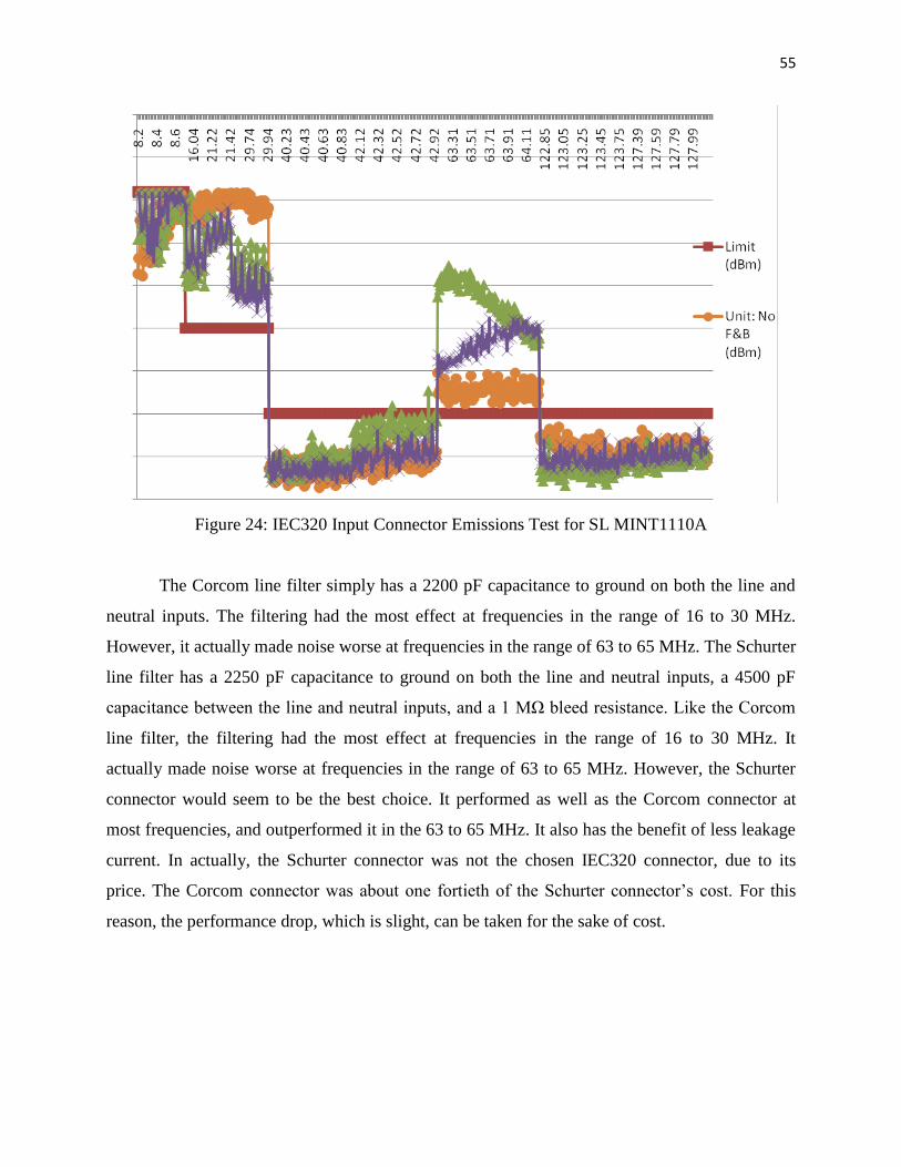
55
Figure 24: IEC320 Input Connector Emissions Test for SL MINT1110A
The Corcom line filter simply has a 2200 pF capacitance to ground on both the line and
neutral inputs. The filtering had the most effect at frequencies in the range of 16 to 30 MHz.
However, it actually made noise worse at frequencies in the range of 63 to 65 MHz. The Schurter
line filter has a 2250 pF capacitance to ground on both the line and neutral inputs, a 4500 pF
capacitance between the line and neutral inputs, and a 1 MΩ bleed resistance. Like the Corcom
line filter, the filtering had the most effect at frequencies in the range of 16 to 30 MHz. It
actually made noise worse at frequencies in the range of 63 to 65 MHz. However, the Schurter
connector would seem to be the best choice. It performed as well as the Corcom connector at
most frequencies, and outperformed it in the 63 to 65 MHz. It also has the benefit of less leakage
current. In actually, the Schurter connector was not the chosen IEC320 connector, due to its
price. The Corcom connector was about one fortieth of the Schurter connector’s cost. For this
reason, the performance drop, which is slight, can be taken for the sake of cost.

56
10.0 Radiation Estimations for Input and Output Wires
One large part of radiated emissions comes from the input and output wires of the power
supply. Two modes of current, which are differential and common mode, can cause emissions
from cabling. Differential mode current results from the difference in current between two wires.
Common mode current is current that travels along both wires in the same direction.
Figure 25: Currents along Two Wires
Figure 25 shows currents along two wires. Ic represents common mode current, while Id
represents the differential mode current. I1 and I2 are the individual currents in each wire. Since
one wire with differential mode current has an opposing direction than the other, it will help
cancel some of the emissions. However, it still plays a significant part in high frequency
emissions on cables. Common mode current does not cancel out. In both cases, a filter can be
introduced to attenuate these EMI generators by returning them back to the source. In order to
understand how much attenuation is needed, there needs to be a way to determine the differential
and common mode currents. They are related by the following equations (Paul, 2006)
Id = 0.5*(I1-I2) eq (7)
Ic = 0.5*(I1+I2) eq (8)
By measuring the currents along each wire, the differential mode and common mode
currents can be calculated. A current probe was connected to an oscilloscope. Using the Fast
Fourier Transform setting of the oscilloscope, the currents measured by the probe was given
according to frequency. In order to measure the differential and common mode current, I1 and I2
needed to be measured. To do this, the current probe simply needed to be aligned on the
corresponding wire in the correction direction. The test setup is shown in Figure 26, and the
results are shown for certain frequencies in Tables 8 through 10. The probe is not as reliable at
frequencies above 100 MHz. However, it can give a relative measure.

57
Figure 26: Current Measurement Test Setup
The next step is to determine the emission levels. The following equations give estimates
emissions in the far field. This means that radiation is the predominant factor for emissions. In
this case, emissions measurements are not in the far field. However, these equations can be
helpful for obtaining information on what mode will be the predominant emissions factor, and
how much so. To calculate the differential mode emissions (Paul, 2006):
(differential mode) Emax = (1.316 x 10⁻¹⁴
|Id| f2 L s) / d eq (9)
where Id is the differential mode current, f is frequency, L is line length, s is line separation, and
d is distance from the wires. To calculate the common mode emissions (Paul, 2006):
(common mode) Emax = (1.257 x 10⁻⁶
|Ic| f L) / d eq (10)
where Ic is the common mode current, f is frequency, L is line length, and d is distance from the
wires.

58

59

60
Figure 27: Differential Mode Emissions on 18V line (dBm vs. Frequency)
Figure 28: Differential Mode Emissions on AC line (dBm vs. Frequency)
Figure 29: Common Mode Emissions on 18V line (dBm vs. Frequency)

61
Figure 30: Common Mode Emissions on AC line (dBm vs. Frequency)
All frequencies shown in Figure 27 through 30 were in Megahertz. The results for
differential mode emissions are reasonable given the baseline emissions tests. This is not the case
for common mode emissions, as they are too high given the baseline emissions tests. These
results do show, however, that common mode current will be the predominant emissions
generator. According to the results, at least 60 dB of attenuation will be needed on the AC input,
but that is uncertain given the overestimate of the results, which is a result of the assumption the
radiation occurs in the far field. The extra attenuation can be used to ensure that the power
supply will not interfere with the MRI. As restrictions on interference in the MRI environment
increase, this will allow for the power supply to continue being used.

62
11.0 Filtering of Conducted Emissions
As stated in section 7.2 Attenuation Models, EMI from the power supply can be
separated into conducted and radiated emissions. Conducted emissions relates to the emissions
generated by cabling of the power supply. Two solutions to this problem are shielding the
cabling or filtering.
In order to lessen emissions on the input and output cables, filters need to be designed.
These filters will lower the high frequencies currents that lead to radiated emission. In filter
design, it is important to look at the flow of current as opposed to voltages. The impedance of a
capacitor is given by the equation 1/jωC, where ω is the frequency and C is the capacitor value.
The impedance of an inductor is given by the equation jωL, where ω is the frequency and L is
the inductor value. With increasing frequency, the impedance of a capacitor decreases while the
impedance of an inductor increases. Current will travel through the path with the least
impedance. The objective of the low pass filter is to block high frequency currents from traveling
through the filter, and instead divert them through the capacitors back to the source. When
radiated emissions testing is conducted with the output line filter, it should show significant
improvement.
Before finding values for the capacitors, inductors, or common mode chokes to be used,
derated values are calculated for each component. Derating is a practice of ensuring component
lifetime. Instead of operating components to their limits, there is a margin that ensures the
components are not being stressed. Below is a table of derating factors, and what maximum
ratings each component selected should have. All derating factors were used from the book
Handbook of Reliability Engineering and Management.
Table 11: Filter Component Values and Derating
Component Aspect Maximum Value from Supply Derating Factor Component Value
Capacitor Voltage 18 Volts 0.6 30 Volts
Capacitor Temperature 0 °C, 50 °C 40 °C to extremes -40 °C, 90 °C
Inductor Voltage 18 Volts 0.7 26 Volts
Inductor Current 5 Amps 0.7 7.14 Amps
The next step is to determine the filter shape and component value. A three pole low pass
filter was decided on. This would provide 60 dB/decade of attenuation (until parasitic effects

63
arise). Two capacitor and one common mode choke would be used. The next step is to create a
model for the filter circuit shown below.
Figure 31: Filter Circuit
The next step is to create the equivalent circuits for both common mode and differential
mode filtering. Figures 32 and 33 are these circuits. (Paul, 2006) Cc1 and Cc2 both represent
capacitors connected from the line to ground. These capacitors will become short circuits at high
frequencies, and will be help attenuate common mode current. Cd1 and Cd2 both represent
capacitors connected from the line to line. Like Cc1 and Cc2, they will act as short circuits across
both lines, and will only attenuate differential mode current. Lchoke is the representation of the
choke’s inductance for each mode. Ideally, the choke will block the common mode current, and
pass all differential mode current. However, this is not actually the case. The inductance of the
choke for the common mode is equal to the sum of the inductance of the separate windings and
their mutual inductance. The inductance of the choke for the differential mode, which is called
the leakage inductance, is equal to the inductance of the separate windings minus their mutual
inductance.
Figure 32: Circuit model for Common Mode Current
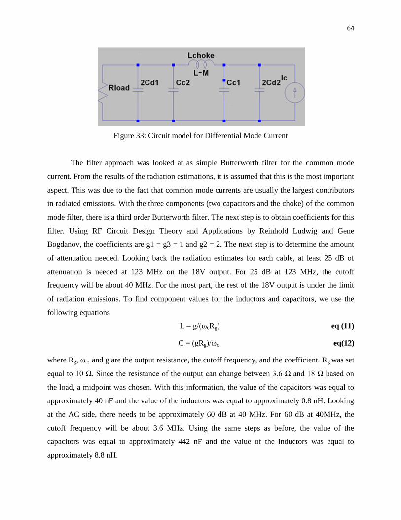
64
Figure 33: Circuit model for Differential Mode Current
The filter approach was looked at as simple Butterworth filter for the common mode
current. From the results of the radiation estimations, it is assumed that this is the most important
aspect. This was due to the fact that common mode currents are usually the largest contributors
in radiated emissions. With the three components (two capacitors and the choke) of the common
mode filter, there is a third order Butterworth filter. The next step is to obtain coefficients for this
filter. Using RF Circuit Design Theory and Applications by Reinhold Ludwig and Gene
Bogdanov, the coefficients are g1 = g3 = 1 and g2 = 2. The next step is to determine the amount
of attenuation needed. Looking back the radiation estimates for each cable, at least 25 dB of
attenuation is needed at 123 MHz on the 18V output. For 25 dB at 123 MHz, the cutoff
frequency will be about 40 MHz. For the most part, the rest of the 18V output is under the limit
of radiation emissions. To find component values for the inductors and capacitors, we use the
following equations
L = g/(ωcRg) eq (11)
C = (gRg)/ωc eq(12)
where Rg, ωc, and g are the output resistance, the cutoff frequency, and the coefficient. Rg was set
equal to 10 Ω. Since the resistance of the output can change between 3.6 Ω and 18 Ω based on
the load, a midpoint was chosen. With this information, the value of the capacitors was equal to
approximately 40 nF and the value of the inductors was equal to approximately 0.8 nH. Looking
at the AC side, there needs to be approximately 60 dB at 40 MHz. For 60 dB at 40MHz, the
cutoff frequency will be about 3.6 MHz. Using the same steps as before, the value of the
capacitors was equal to approximately 442 nF and the value of the inductors was equal to
approximately 8.8 nH.

65
From the circuits in figure 32 and 33, the expected attenuation can be found. First, the
circuit below is the starting point.
Figure 34: General Filter Circuit model
Now solve for the attenuation (i3/i):
i = i1 + i2 + i3
Rloadi3 = i2Zcap1 => i2 = (Rload/ Zcap1)i3
i – i1 = i3(Rload/ Zcap1 +1)
i1Zcap2 = Zchoke(i-i1) + Rloadi3 = Zchoke i3(Rload/ Zcap1 +1)+ Rloadi3
i1 = (i3/Zcap2) [Zchoke (Rload/ Zcap1 +1)+ Rload]
i – i2 - i3 = i - i3(Rload/ Zcap1 +1) = (i3/Zcap2) [Zchoke (Rload/ Zcap1 +1)+ Rload]
i = i3[(1/Zcap2) [Zchoke (Rload/ Zcap1 +1)+ Rload] + (Rload/ Zcap1 +1)] eq (13)
There are multiple issues with the values of the components found with the Butterworth
coefficients. First, the common mode choke that needs to be used is an air core. The reason for
this is that an air core inductor will lessen the chance of any failures in the magnetic field of the
MRI. The minimum air core choke for the 18V side was 100 μH (Gowanda CMF4-1003H). The
capacitor values will also need to be changed because of parasitic properties. For the 18V output,
a 0.1 μF capacitor (AVX Corp 22255A104FAT2A) will become a short circuit around the 10 to
100 MHz range.
Using equation 13, a model both the common mode and differential mode attenuation can
be found. This was simply the ratio of output to input current in dB. Figures 35 and 36 show this
expected attenuation. You’ll see that in both graphs that the noise is attenuated well beyond the
needs of current MRI technology. However, to extend the longevity of this product, additional
attenuation will actually be desirable.

66
35: Differential Mode Attenuation on 18V Line
Figure 36: Common Mode Attenuation on 18V Line
Even though the 18 Volt output filter somewhat followed the Butterworth design, the AC
input filter will not. The first reason is the inductor. Again, air core common mode chokes are
preferable for the MRI environment. However, air core common mode chokes rated for the AC
line were not found. So, a common mode choke was not included in the input filter. Another
limitation of the input filter are in capacitor values. In order to follow regulations, the power
supply cannot generate more than 500 μA of leakage current to the ground. Original datasheets
of the SL MINT1110A showed the supply to generate less than 50 μA. An updated datasheet
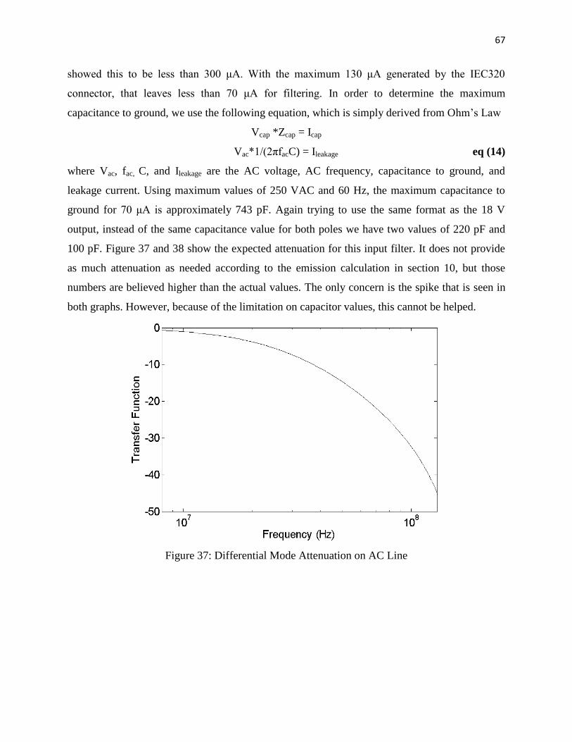
67
showed this to be less than 300 μA. With the maximum 130 μA generated by the IEC320
connector, that leaves less than 70 μA for filtering. In order to determine the maximum
capacitance to ground, we use the following equation, which is simply derived from Ohm’s Law
Vcap *Zcap = Icap
Vac*1/(2πfacC) = Ileakage eq (14)
where Vac, fac, C, and Ileakage are the AC voltage, AC frequency, capacitance to ground, and
leakage current. Using maximum values of 250 VAC and 60 Hz, the maximum capacitance to
ground for 70 μA is approximately 743 pF. Again trying to use the same format as the 18 V
output, instead of the same capacitance value for both poles we have two values of 220 pF and
100 pF. Figure 37 and 38 show the expected attenuation for this input filter. It does not provide
as much attenuation as needed according to the emission calculation in section 10, but those
numbers are believed higher than the actual values. The only concern is the spike that is seen in
both graphs. However, because of the limitation on capacitor values, this cannot be helped.
Figure 37: Differential Mode Attenuation on AC Line

68
Figure 38: Common Mode Attenuation on AC Line
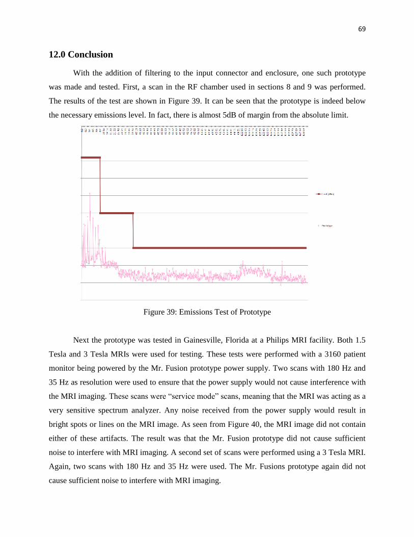
69
12.0 Conclusion
With the addition of filtering to the input connector and enclosure, one such prototype
was made and tested. First, a scan in the RF chamber used in sections 8 and 9 was performed.
The results of the test are shown in Figure 39. It can be seen that the prototype is indeed below
the necessary emissions level. In fact, there is almost 5dB of margin from the absolute limit.
Figure 39: Emissions Test of Prototype
Next the prototype was tested in Gainesville, Florida at a Philips MRI facility. Both 1.5
Tesla and 3 Tesla MRIs were used for testing. These tests were performed with a 3160 patient
monitor being powered by the Mr. Fusion prototype power supply. Two scans with 180 Hz and
35 Hz as resolution were used to ensure that the power supply would not cause interference with
the MRI imaging. These scans were “service mode” scans, meaning that the MRI was acting as a
very sensitive spectrum analyzer. Any noise received from the power supply would result in
bright spots or lines on the MRI image. As seen from Figure 40, the MRI image did not contain
either of these artifacts. The result was that the Mr. Fusion prototype did not cause sufficient
noise to interfere with MRI imaging. A second set of scans were performed using a 3 Tesla MRI.
Again, two scans with 180 Hz and 35 Hz were used. The Mr. Fusions prototype again did not
cause sufficient noise to interfere with MRI imaging.

70
Figure 40: MRI Scan Result
These results are encouraging. However, due to a change in the SL MINT1110A’s
datasheet, the input filtering used more capacitance to ground. Because of the limited amount of
time left, this was not completed before the end of D term. However, there will be a prototype
made at some point, and the same testing will be repeated. Additional testing from section 5 will
be performed to ensure that this product will be safe for consumers, and will be compliant with
all regulations. With this complete, this project may result in a product that will be used for MRI
patient monitoring.

71
Sources
Barnes, John. (1992) Electronic System Design: Interference and Noise Control Techniques.
Prentice-Hall, Inc.
Brown, Mark, Semelka, Richard. (1999) MRI Basic Principles and Applications, Second
Edition. Wiley-Liss, Inc.
Clayton, Paul. (2006) Introduction to Electromagnetic Compatibility. John Wiley & Sons, Inc.
Haacke, Mark, Brown, Robert, Thompson, Michael, Venkatesan, Ramesh. (1999) Magnetic
Resonance Imaging Physical Principles and Sequence Design. Wiley-Liss, Inc.
Hemming, Leland. (1992) Architectural Electromagnetic Shielding Handbook. Institute of
Electrical and Electronics Engineers, Inc.
Hornak, Joseph. (1996-2008) The Basics of MRI. http://www.cis.rit.edu/htbooks/mri/index.html
Overweg, Johan. (2006) MRI Magnet Design, Modeling. Philips Research.

72
Appendix A


Embedded Power forBusiness-Critical Continuity
NFS110 MedicalSeriesSingle and quad output
Special Features• 7.0 x 4.25 x 1.8 inch package• Medical, dental and
laboratory applications• Overvoltage and short circuit
protection• 110 W with 20 CFM• UL, VDE and CSA safety
approvals• EN60601-1 and UL2601
medical approvals• Available RoHS compliant• 2 year warranty
Total Power: 80 - 110 WInput Voltage: 90 - 253 Vac
127 - 357 Vdc# of Outputs: Single, quad
SafetyVDE0805/EN60601-1/IEC601/IEC1010 File No. 10401-3336-1049 Licence No. 2874
UL2601 File No. E147937
CSA C22.2 No. 125 File No. LR41062C
Rev. 06.10.08
NFS110 Series
1 of 5
Electrical SpecificationsOutput
Voltage adjustability +5.1 V o/p on multi’s ±3.0%5.1 V single output ±3.0%12 V single output 12-14 V15 V single output 15-18 V24 V single output 24-30 V
Line regulation LL to HL, FL ±0.1% max.All outputs on all units
Overshoot/undershoot At turn-on no lead 0%Temperature coefficient All outputs ±0.02%/°COvervoltage protection Multi o/p 5.1 V only 6.25 V ±0.75 V
5.1 V single 6.25 V ±0.75 V12 V single 15.75 V ±1.0 V15 V single 22 V ±1.5 V24 V single 33 V ±2.5 V
Output power limit Primary power Pin max. 160 Wlimited Pout min. 110 W
Short circuit protection Burst mode operation
InputInput voltage range 90-253 Vac
127-357 Vdc
Input frequency range 47-440 Hz
Input surge current 110 Vac. 50 Hz 17 A230 Vac. 50 Hz 35 A
Safety ground leakage current 132 Vac 50 μA264 Vac 100 μA
All specifications are typical at nominal input, full load at
25°C unless otherwise stated
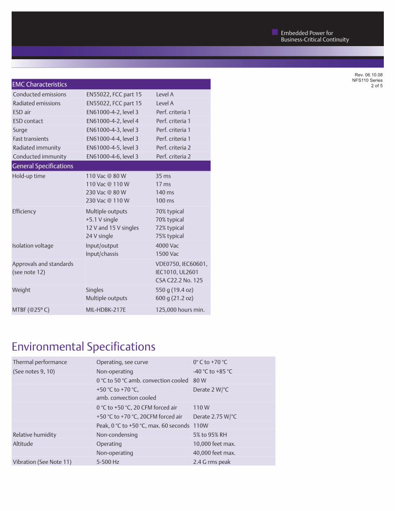
Rev. 06.10.08
NFS110 Series
2 of 5
Embedded Power forBusiness-Critical Continuity
Environmental SpecificationsThermal performance Operating, see curve 0° C to +70 °C
(See notes 9, 10) Non-operating -40 °C to +85 °C
0 °C to 50 °C amb. convection cooled 80 W
+50 °C to +70 °C, amb. convection cooled
Derate 2 W/°C
0 °C to +50 °C, 20 CFM forced air 110 W
+50 °C to +70 °C, 20CFM forced air Derate 2.75 W/°C
Peak, 0 °C to +50 °C, max. 60 seconds 110W
Relative humidity Non-condensing 5% to 95% RH
Altitude Operating 10,000 feet max.
Non-operating 40,000 feet max.
Vibration (See Note 11) 5-500 Hz 2.4 G rms peak
EMC Characteristics
Conducted emissions EN55022, FCC part 15 Level A
Radiated emissions EN55022, FCC part 15 Level A
ESD air EN61000-4-2, level 3 Perf. criteria 1
ESD contact EN61000-4-2, level 4 Perf. criteria 1
Surge EN61000-4-3, level 3 Perf. criteria 1
Fast transients EN61000-4-4, level 3 Perf. criteria 1
Radiated immunity EN61000-4-5, level 3 Perf. criteria 2
Conducted immunity EN61000-4-6, level 3 Perf. criteria 2
General Specifications
Hold-up time 110 Vac @ 80 W 35 ms110 Vac @ 110 W 17 ms230 Vac @ 80 W 140 ms230 Vac @ 110 W 100 ms
Efficiency Multiple outputs 70% typical+5.1 V single 70% typical12 V and 15 V singles 72% typical24 V single 75% typical
Isolation voltage Input/output 4000 VacInput/chassis 1500 Vac
Approvals and standards(see note 12)
VDE0750, IEC60601, IEC1010, UL2601CSA C22.2 No. 125
Weight Singles 550 g (19.4 oz)Multiple outputs 600 g (21.2 oz)
MTBF (@25º C) MIL-HDBK-217E 125,000 hours min.

Rev. 06.10.08
NFS110 Series
3 of 5
Embedded Power forBusiness-Critical Continuity
Notes1 Convection cooled, 80 W maximum.2 Peak outputs lasting less than 60 seconds with duty cycle less than 10%. Total
peak power must not exceed 110 W.3 Forced air, 20 CFM at 1 atmosphere, 110 W maximum.4 Figure is peak-to-peak. Output ripple is measured across a 50 MHz bandwidth
using a 12 inch twisted pair terminated with a 47 μF capacitor.5 Total regulation is defined at the static output regulation at 25 °C, including
initial tolerance, line voltage within stated limits and output voltages adjustedto their factory settings. Also for NFS110-7902PJ, for 24 V output statedregulation IA / IB ² 5. This output will maintain ±5.0% regulation if IA ² 5 A, where IA = +5.1 V output current and IB = +24 V output current.
6 Single output models have floating outputs which may be referenced as eitherpositive or negative. Higher voltage supplies, may be adjusted over a wideoutput voltage range, as long as the total output power does not exceed 80Watts (natural convection) or 110 Watts (forced air).
7 Power fail detect not available on single output models.8 Derating curve is application specific for ambient temperatures > 50 °C, for
optimum reliability no part of the heatsink should exceed 90 °C and nosemiconductor case temperature should exceed 100 °C.
9 Caution: Allow a minimum of 1 second after disconnecting the power whenmaking thermal measurements.
10 The user should read the PSU installation instructions in conjunction with therelevant national safety regulations in order to ensure compliance.
11 Three orthogonal axes, random vibration, 10 minute test for each axis.12 This product is only for inclusion by professional installers within other
equipment and must not be operated as a stand alone product.13 The ‘J’ suffix indicates that these parts are Pb-free (RoHS 6/6) compliant. TSE
RoHS 5/6 (non Pb-free) compliant versions may be available on special request,please contact your local sales representative for details.
14 NOTICE: Some models do not support all options. Please contact your localEmerson Network Power representative or use the on-line model numbersearch tool at http://www.powerconversion.com to find a suitable alternative.
TRANSIENT RESPONSE
NFS110-7901PJ +5.1 V (7.5-10 A) 150 mV peak,1 ms recovery
+12 V (2.5-5 A) 100 mV peak,0.5 ms recovery
-12 V (0.5-1 A) 100 mV peak,0.5 ms recovery
-5 V (0.5-1 A) 100 mV peak,0.5 ms recovery
NFS110-7902PJ +5.1 V (7.5-10 A) 150 mV peak,1 ms recovery
+12 V (2.5-5 A) 100 mV peak,0.5 ms recovery
-12 V (0.5-1 A) 100 mV peak,0.5 ms recovery
24 V (1.5-3 A) 300 mV peak,1 ms recovery
NFS110-7904PJ +5.1 V (7.5-10 A) 150 mV peak,1 ms recovery
+15 V (2.5-5 A) 100 mV peak,0.5 ms recovery
-15 V (0.5-1 A) 100 mV peak,0.5 ms recovery
-5 V (0.5-1 A) 100 mV peak,0.5 ms recovery
NFS110-7905J +5.1 V (10-20 A) 250 mV peak,1 ms recovery
NFS110-7912J +12 V (4.5-9 A) 360 mV peak,1 ms recovery
NFS110-7915J +15 V (3.65-7.3 A) 450 mV peak,1 ms recovery
NFS110-7924J +24 V (2.25-4.5 A) 720 mV peak,
Ordering Information
Output
Voltage
Output Currents
Ripple (4)
Total
Regulation (5) Model Numbers (13, 14, F)Max (1) Peak (2) Fan (3)
+5.1 V 8 A 20 A 10 A 50 mV ±2.0% NFS110-7901PJ
+12 V 4.5 A 9 A 5 A 120 mV ±3.0%
–12 V 0.5 A 1.5 A 1 A 120 mV ±3.0%
–5 V 0.5 A 1.5 A 1 A 50 mV ±3.0%
+5.1 V (IA) 8 A 20 A 10 A 50 mV ±2.0% NFS110-7902PJ
+24 V (IB) (6) 3.5 A 4.5 A 4.5 A 240 mV +10/–5.0%
+12 V 4.5 A 9 A 5 A 120 mV ±3.0%
–12 V 0.5 A 1.5 A 1 A 120 mV ±3.0%
+5.1 V 8 A 20 A 10 A 50 mV ±2.0% NFS110-7904PJ
+15 V 4 A 7.5 A 5 A 150 mV ±4.0%
–15 V 0.5 A 1.5 A 1 A 150 mV ±3.0%
–5 V 0.5 A 1.5 A 1 A 50 mV ±3.0%
12 V 7 A 9 A 9 A 120 mV ±2.0% NFS110-7912J (7,8)
15 V 5 A 7.3 A 7.3 A 150 mV ±2.0% NFS110-7915J (7,8)
24 V 3.5 A 4.5 A 4.5 A 240 mV ±2.0% NFS110-7924J (7,8)
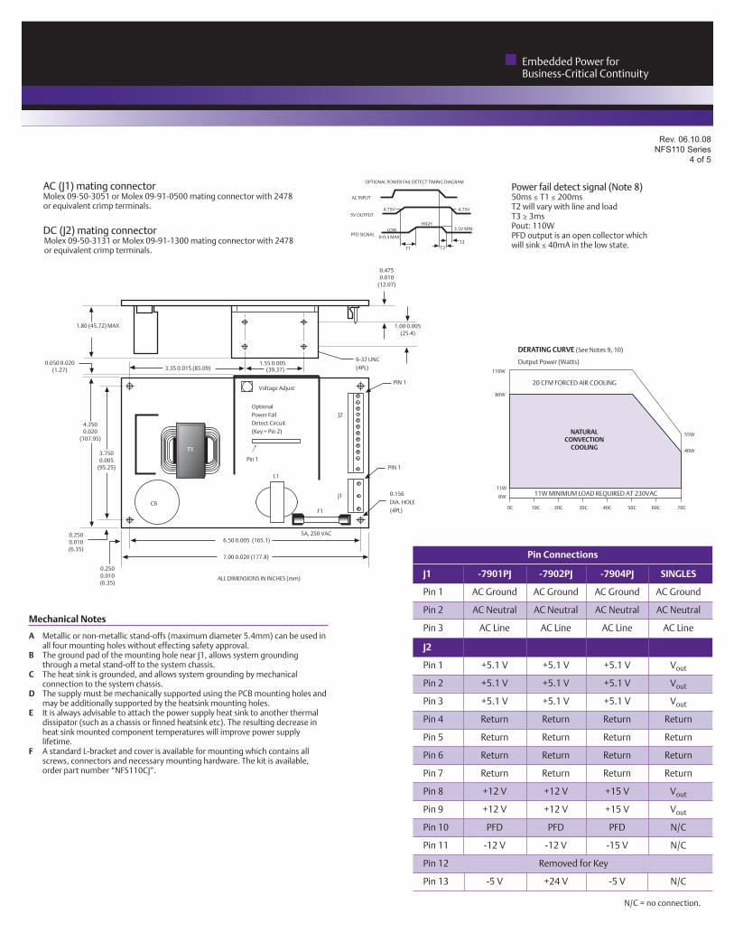
Rev. 06.10.08
NFS110 Series
4 of 5
Embedded Power forBusiness-Critical Continuity
AC (J1) mating connectorMolex 09-50-3051 or Molex 09-91-0500 mating connector with 2478or equivalent crimp terminals.
DC (J2) mating connectorMolex 09-50-3131 or Molex 09-91-1300 mating connector with 2478or equivalent crimp terminals.
ALL DIMENSIONS IN INCHES (mm)
OptionalPower FailDetect Circuit(Key = Pin 2)
Pin 1
6-32 UNC(4PL)
PIN 1
1.00 0.005(25.4)
Voltage Adjust
J2
J1
F1
L1
T1
C6
PIN 1
0.156DIA. HOLE(4PL)
5A, 250 VAC
0.4750.010
(12.07)
1.55 0.005(39.37)3.35 0.015 (85.09)
1.80 (45.72) MAX
0.050 0.020(1.27)
4.250 0.020
(107.95)
3.750 0.005
(95.25)
0.250 0.010(6.35)
0.250 0.010(6.35)
6.50 0.005 (165.1)
7.00 0.020 (177.8)
T1
Power fail detect signal (Note 8)50ms ≤ T1 ≤ 200msT2 will vary with line and loadT3 ≥ 3msPout: 110WPFD output is an open collector whichwill sink ≤ 40mA in the low state.
HIGH
T1 T2T3
4.75V
3.5V MIN
0-0.4 MAX
LOW
4.75V5V OUTPUT
PFD SIGNAL
AC INPUT
OPTIONAL POWER FAIL DETECT TIMING DIAGRAM
80W
20 CFM FORCED AIR COOLING
40W
55W
0W
11W11W MINIMUM LOAD REQUIRED AT 230VAC
NATURAL CONVECTION
COOLING
0C 10C 20C 30C 40C 50C 60C 70C
DERATING CURVE (See Notes 9, 10)
Output Power (Watts)110W
N/C = no connection.
Pin Connections
J1 -7901PJ -7902PJ -7904PJ SINGLES
Pin 1 AC Ground AC Ground AC Ground AC Ground
Pin 2 AC Neutral AC Neutral AC Neutral AC Neutral
Pin 3 AC Line AC Line AC Line AC Line
J2
Pin 1 +5.1 V +5.1 V +5.1 V Vout
Pin 2 +5.1 V +5.1 V +5.1 V Vout
Pin 3 +5.1 V +5.1 V +5.1 V Vout
Pin 4 Return Return Return Return
Pin 5 Return Return Return Return
Pin 6 Return Return Return Return
Pin 7 Return Return Return Return
Pin 8 +12 V +12 V +15 V Vout
Pin 9 +12 V +12 V +15 V Vout
Pin 10 PFD PFD PFD N/C
Pin 11 -12 V -12 V -15 V N/C
Pin 12 Removed for Key
Pin 13 -5 V +24 V -5 V N/C
Mechanical Notes
A Metallic or non-metallic stand-offs (maximum diameter 5.4mm) can be used inall four mounting holes without effecting safety approval.
B The ground pad of the mounting hole near J1, allows system groundingthrough a metal stand-off to the system chassis.
C The heat sink is grounded, and allows system grounding by mechanicalconnection to the system chassis.
D The supply must be mechanically supported using the PCB mounting holes andmay be additionally supported by the heatsink mounting holes.
E It is always advisable to attach the power supply heat sink to another thermaldissipator (such as a chassis or finned heatsink etc). The resulting decrease inheat sink mounted component temperatures will improve power supplylifetime.
F A standard L-bracket and cover is available for mounting which contains allscrews, connectors and necessary mounting hardware. The kit is available,order part number “NFS110CJ” .

Americas 5810 Van Allen WayCarlsbad, CA 92008USATelephone: +1 (760) 930 4600Facsimile: +1 (760) 930 0698
Europe (UK)Waterfront Business ParkMerry Hill, DudleyWest Midlands, DY5 1LXUnited KingdomTelephone: +44 (0) 1384 842 211Facsimile: +44 (0) 1384 843 355
Asia (HK)14/F, Lu Plaza2 Wing Yip StreetKwun Tong, KowloonHong KongTelephone: +852 2176 3333Facsimile: +852 2176 3888
For global contact, visit:[email protected] every precaution has been taken to ensure accuracy and completeness in this literature, EmersonNetwork Power assumes no responsibility, and disclaims all liability for damages resulting from use of this information or for any errors or omissions.
Embedded Power forBusiness-Critical Continuity
Rev. 06.10.08
NFS110 Series
5 of 5
Emerson Network Power and the EmersonNetwork Power logo are trademarks andservice marks of Emerson Electric Co.©2008 Emerson Electric Co.
EmersonNetworkPower. com
Embedded Computing
Embedded Power
Monitoring
Outside Plant
Power Switching & Controls
Precision CoolingRacks & Integrated Cabinets
Services
Surge Protection
Emerson Network Power. The global leader in enablingbusiness-critical continuity.
AC Power
Connectivity
DC Power

Embedded Power forBusiness-Critical Continuity
LPS170-M SeriesMedical175 Watts
Special Features• Medical safety approvals• Active power factor correction• IEC EN61000-3-2 compliance• Wide Range Adjustable output
Remote sense on main output• Single wire current sharing• Power fail and remote inhibit • Built-in EMI filter• Low output ripple• Overvoltage protection• Overload protection• Thermal overload protection• DC power good• 5 V standby output• 12 V Aux output• Optional cover (-C suffix)
Total Power: 100 - 175 WattsInput Voltage: 85-264 VAC
120-300 VDC# of Outputs: Single
Electrical Specifications
Safety
InputInput ra nge 85-264 VAC; 120-300 VDC
Frequency 47-67 Hz
Inrush current 38 A max, cold start @ 25°C
Efficiency 75% typical at full loadEMI filter FCC Class B conducted
CISPR 22 Class B conductedEN55022 Class B conductedVDE 0878 PT3 Class B conducted
Power Factor 0.99 typical
Safety ground leakage current
<250 μA @ 50/60 Hz, 264 VAC inputS
OutputMaximum power 110 W convection (75 W with cover)
175 W with 30 CFM forced air (130 W with cover)
Adjustment range 2:1 wide ratio minimum
Standby outputs 5 V @ 2 A regulated ±5%Hold-up time 20 ms @175 W load at nominal line
Overload protection Short circuit protection on all outputs. Case overload protected @ 110-145% above peak rating
Overvoltage protection 10% to 40% above nominal output
Aux output 12 V @ 1 A -5 %, +10%
VDE 0750/EN60601-1 (IEC601)UL UL2601CSA CSA 22.2 No. 601.1CE Mark (LVD)
Rev. 08.07.07
LPS170-M Series
1 of 3
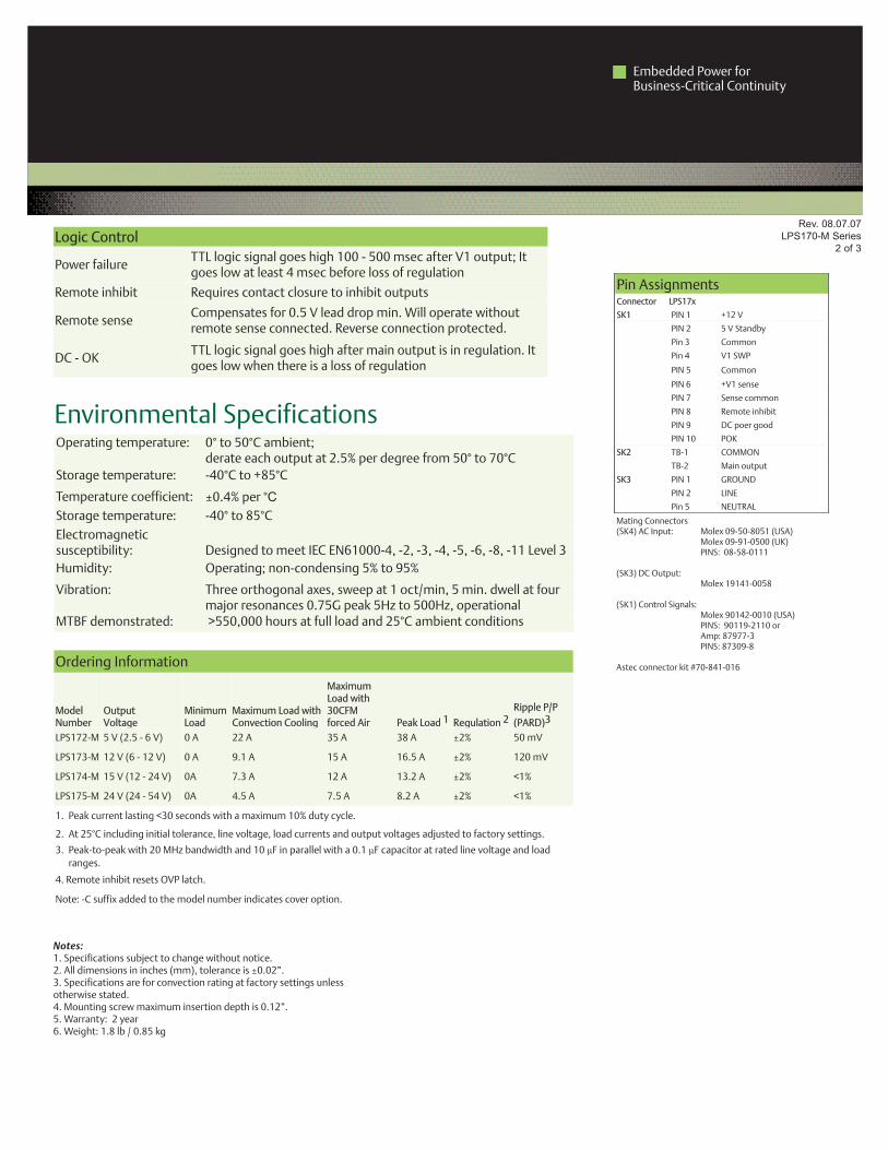
Embedded Power forBusiness-Critical Continuity
Ordering Information
ModelNumber
OutputVoltage
Minimum Load
Maximum Load withConvection Cooling
MaximumLoad with30CFM forced Air Peak Load 1 Regulation 2
Ripple P/P
(PARD)3
LPS172-M 5 V (2.5 - 6 V) 0 A 22 A 35 A 38 A ±2% 50 mV
LPS173-M 12 V (6 - 12 V) 0 A 9.1 A 15 A 16.5 A ±2% 120 mV
LPS174-M 15 V (12 - 24 V) 0A 7.3 A 12 A 13.2 A ±2% <1%
LPS175-M 24 V (24 - 54 V) 0A 4.5 A 7.5 A 8.2 A ±2% <1%
1. Peak current lasting <30 seconds with a maximum 10% duty cycle.
2. At 25°C including initial tolerance, line voltage, load currents and output voltages adjusted to factory settings.
3. Peak-to-peak with 20 MHz bandwidth and 10 μF in parallel with a 0.1 μF capacitor at rated line voltage and loadranges.
4. Remote inhibit resets OVP latch.
Note: -C suffix added to the model number indicates cover option.
Rev. 08.07.07
LPS170-M Series
2 of 3
Operating temperature: 0° to 50°C ambient;derate each output at 2.5% per degree from 50° to 70°C
Storage temperature: -40°C to +85°C
Temperature coefficient: ±0.4% per °CStorage temperature: -40° to 85°CElectromagnetic susceptibility: Designed to meet IEC EN61000-4, -2, -3, -4, -5, -6, -8, -11 Level 3Humidity: Operating; non-condensing 5% to 95%
Vibration: Three orthogonal axes, sweep at 1 oct/min, 5 min. dwell at fourmajor resonances 0.75G peak 5Hz to 500Hz, operational
MTBF demonstrated: >550,000 hours at full load and 25°C ambient conditions
Environmental Specifications
Logic Control
Power failureTTL logic signal goes high 100 - 500 msec after V1 output; Itgoes low at least 4 msec before loss of regulation
Remote inhibit Requires contact closure to inhibit outputs
Remote senseCompensates for 0.5 V lead drop min. Will operate withoutremote sense connected. Reverse connection protected.
DC - OKTTL logic signal goes high after main output is in regulation. Itgoes low when there is a loss of regulation
Mating Connectors(SK4) AC Input: Molex 09-50-8051 (USA)
Molex 09-91-0500 (UK)PINS: 08-58-0111
(SK3) DC Output:Molex 19141-0058
(SK1) Control Signals:Molex 90142-0010 (USA)PINS: 90119-2110 orAmp: 87977-3PINS: 87309-8
Astec connector kit #70-841-016
Notes:1. Specifications subject to change without notice.2. All dimensions in inches (mm), tolerance is ±0.02”.3. Specifications are for convection rating at factory settings unless otherwise stated.4. Mounting screw maximum insertion depth is 0.12”.5. Warranty: 2 year6. Weight: 1.8 lb / 0.85 kg
Pin AssignmentsConnector LPS17x
SK1 PIN 1 +12 V
PIN 2 5 V Standby
Pin 3 Common
Pin 4 V1 SWP
PIN 5 Common
PIN 6 +V1 sense
PIN 7 Sense common
PIN 8 Remote inhibit
PIN 9 DC poer good
PIN 10 POK
SK2 TB-1 COMMON
TB-2 Main output
SK3 PIN 1 GROUND
PIN 2 LINE
Pin 5 NEUTRAL

Emerson Network Power and the EmersonNetwork Power logo are trademarks andservice marks of Emerson Electric Co.©2007 Emerson Electric Co.
Embedded Power forBusiness-Critical Continuity
Emerson Network Power. The global leader in enablingbusiness-critical continuity.
EmersonNetworkPower. com
AC Power
Connectivity
DC Power
Embedded Power
Inbound Power
Integrated Cabinet SolutionsOutside Plant
Precision Cooling
Site Monitoring and Services
Americas 5810 Van Allen WayCarlsbad, CA 92008USATelephone: +1 760 930 4600Facsimile: +1 760 930 0698
Europe (UK)Waterfront Business ParkMerry Hill, DudleyWest Midlands, DY5 1LXUnited KingdomTelephone: +44 (0) 1384 842 211Facsimile: +44 (0) 1384 843 355
Asia (HK)16th - 17th Floors, Lu Plaza2 Wing Yip Street, Kwun TongKowloon, Hong KongTelephone: +852 2176 3333Facsimile: +852 2176 3888
For global contact, visit:www.astecpower.comwww.artesyn.comtechnicalsupport@[email protected] every precaution has been taken to ensure accuracy and completeness in this literature, EmersonNetwork Power assumes no responsibility, and disclaims all liability for damages resulting from use of this information or for any errors or omissions.
Rev. 08.07.07
LPS170-M Series
3 of 3Mechanical Drawing

Engineering Specification – 110W, MINT1110A Medical Family
Preliminary 9-2008
Typical 85% efficiency
Less than 1.27” height
EN60601-1 Medical approval
Rugged, EMC compliant design
OUTPUT SPECIFICATIONS
Total regulation (Line and load): +/- 2%
Turn-on time: < 2S
Hold up time: 16mS minimum from loss of AC input at full load,
nominal line (120Vac/60 Hz)
Ripple & noise: p-p max
Transient response: 0.5 msec. for 50% load change typical
Input connector: 2 Pin LANDWIN P/N 3361P03E3TSN02
Output connector: 4 Pin LANDWIN P/N 3361P04E3T
Earth Ground connection to be via 0.187” faston tab
P/N 3201T122R LANDWIN
INPUT SPECIFICATIONS
Input voltage: 100-240 VAC, +/-10%
Input frequency: 47-63Hz
Input current: 1.4A max. at 115 VAC input
Input surge current: 264Vac (Cold start) 30A max
Input fuse: UL/IEC127 T3.15A, 250Vac
Power factor: IEC61000-3-2
Leakage current: 115Vac@60Hz <50uA
Input configuration:
GENERAL SPECIFICATIONS
Efficiency: up to 90% typically
Isolation voltage: Input/output 4000Vac
Input/Earth 1800Vac
Output/Earth 500Vac
Safety approval: UL2601, CSA 22.2 No. 601.1-M90,
IEC 601-1 (1988), EN 60601-1(1999):
EMC SPECIFICATIONS
Conducted emissions:
FCC Part 18 Subpart B / EN55011 Class B
Radiated emissions:
FCC Part 18 Subpart B / EN55011 Class B
ESD air: IEC 61000-4-2, 15kV
ESD contact: IEC 61000-4-2, 8kV
Conducted immunity: IEC61000-4-6, 3Vrms
Radiated immunity: IEC 61000-4-3, 10V/m
Fast transients: IEC 61000-4-4, 2kV/5kHz
Surge: IEC 61000-4-5, 1kV Differential, 2kV Common
Power freq. Mag. Field: IEC61000-4-8, 3A/m
Voltage dip immunity: IEC61000-4-11 240Vac, 0%/0.5 cycle,
40%/5cycles, 70%/25 cycles
PROTECTION SPECIFICATIONS
Over current protection: Hiccup mode
Short circuit protection: Hiccup mode.
Over voltage protection: Built-in, latch off
Over temperature protection: Option
MECHANICAL SPECIFICATIONS
Dimensions: W 3.0”X L5.0”x H 1.2”
See Figure 1
Weight: TBD gm
ENVIROMENT SPECIFICATIONS
Operating temp.: 0-70°C
Storage temp.: -40-+85°C
Relative humidity: 0%-95%
Altitude: Operating: -500 to 10,000 ft. MSL
Non-Operating: -500 to 40,000 ft .MSL
Model Output
Voltage
Output
Current
50°°°°C
Output
Current
60°°°°C (1)
Total
Regulation
Initial
Set point
Tolerance
OVP
Limit
Ripple or
Noise Pk-Pk(max)
MINT1110A1208K01 12V 7.5A 8,3A 2% 1% 15±1V 1%
MINT1110A1508K01 15V 6.5A 7.2A 2% 1% 18±1V 1%
MINT1110A1808K01 18V 5.8A 6.3A 2% 1% 23±1V 1%
MINT1110A2408K01 24V 4.6A 4.8A 2% 1% 28±1V 1%

Engineering Specification – 110W, MINT1110A Medical Family
Preliminary 9-2008
Fig. 1
Input Connector – J1
Pin 1 AC Line
Pin 2 AC Neutral
J1 Mates with AMP MTA-156 3P connector (Middle Pin Removed)
J2 Mates with AMP MTA-156 8P Connector
Output Connector – J2
Pin Single
1 +V1
2 +V1
3 +V1
4 +V1
5 RTN
6 RTN
7 RTN
8 RTN

Design and specifi cations are each subject to change without notice. Ask factory for the current technical specifi cations before purchase and/or use.Should a safety concern arise regarding this product, please be sure to contact us immediately.
Ceramic Disc Capacitors (Safety Regulations)
E
1
C
2
K
3 4 5 6 7 8 9 10 11 12
Product CodeClassClass 1Class 2
CodeECCECK
SuffixType NameCodeNATSVS
TypeType NS-AType TSType VS
CodeGBEF
Char.SL/GPB/Y5PE/Y5UF/Y5V
Temp. CharLead StyleCode
A
N
StyleKinked LeadBulkKinked LeadTaped
Cap.100 pF
1000 pF2200 pF4700 pF
10000 pF
Nominal Capacitance
N T S 1 0 2 M E
Ex.101102222472103
Cap. Tol.±5 %
±10 %±20 %
+80, –20 %
Cap. ToleranceCode
JKMZ
Ceramic Disc Capacitors (Safety Regulations)
Type NS-A IEC60384-14 Sub-class Y1/X1, UL, CSAType TS IEC60384-14 Sub-class Y2/X1, UL, CSAType VS IEC60384-14 Sub-class Y2/X1, UL, CSA Smaller size
Recommended Applications Interference suppressors for IT equipment (for eg.
Modem) Interference suppressors for AC Primary Line of electronic
equipment (Switching power supplies, Inverter type lighting apparatus etc.)
Other electronic equipment for AC primary Line.
Features Related by IEC60384-14 2nd Ed. and approved by
European Safety Regulations (Types NS-A, TS and VS) Reinforced Body Insulation /0.4mm min. approved by
BSI, VDE (Type NS-A, Y1, Reinforced Insulation) Flame-retardant insulated coating Easy mounting through kinked leads and radial tap ing
Explanation of Part Numbers
Specifi cations
Characteristics Type NS-A Type TS Type VS
RelatedStandards
IEC 60384-14(Y1/,X1) BSI, VDE, SEV, SEMKO FIMKO, NEMKO, DEMKOUL,CSA, KTL
IEC 60384-14(Y2/,X1) BSI, VDE, SEV, SEMKO FIMKO, NEMKO, DEMKOUL,CSA, KTL
IEC 60384-14(Y2/, X1) VDE, SEMKO, FIMKO NEMKO, DEMKOUL, KTL
OperatingTemperature Range –25 to 125 °C
Rated Voltage 250 VAC/440 VAC
Dielectric WithstandingVoltage
4000 VAC for 1 minute 2600 VAC for 1 minute 1500 VAC for 1 minute
Capacitance Within the tolerance, when mea sured at 1 kHz ± 20 %, 1 Vrms, and 20 °C
Q (Temp. Char. SL) 30 pF or under Q > 400+20C (C : Cap. pF)over 30 pF Q > 1000 at 1 MHz ±20 % 1 to 5 Vrms. and 20 °C
DissipationFactor(tand)
tan d < 0.025, when measured at 1 kHz ±20 %, 1 Vrms, and 20 °C
Insulation Resistance 10000 M min at 500 VDC 1 minute electrifi cation.
TemperatureCharacteristics
Char. max. Cap. Change Temperature RangeSL/GP +350 to –1000 ppm/°C 20 to 85 °CB/Y5P ±10 % –25 to 85 °CE/Y5U +20, –55 % –25 to 85 °CF/Y5V +30, –80 % –25 to 85 °C
Feb. 2006

Design and specifi cations are each subject to change without notice. Ask factory for the current technical specifi cations before purchase and/or use.Should a safety concern arise regarding this product, please be sure to contact us immediately.
Ceramic Disc Capacitors (Safety Regulations)
Related Standards and Certifi cate Numbers Type NS-A
Certifying Body Related Standard Certifi cateNumber
Sub-class
RatedVoltage
DielectricWithstanding
Voltage
OperatingTemperature
RangeBSI (UK)
EN 132 400:1994Sub-class Y2(IEC 60384-14 2nd Ed.)
226319
Y1, X1 Y1:250 VACX1:440 VAC
Y1:4000 VACX1:1892 VDC –25 to 125 °C
VDE (Germany) 087472SEV (Switzerland) 05.0123SEMKO (Sweden) 9918234/01-02FIMKO (Finland) F1 13556NEMKO (Norway) P99101676DEMKO (Denmark) DK99-02495KTL (Korea) K60384-14 (IEC 60384-14 2nd Ed.) SU03012-3002UL (USA) UL1414 E62674
— 250 VAC 1500 VAC –25 to 85 °CCSA (Canada) CSA C22.2 No.1 LR58064Note:Certifi cation Number sometimes changes with the change of the approval contents and so on. CQC and KTL marks are indicated on the label. Type TS
Certifying Body Related StandardCertifi cate Number Sub-
classRated
VoltageDielectric
WithstandingVoltage
OperatingTemperature
RangePlant Code H Plant Code MBSI (UK)
EN132 400:1994Sub-class Y2
(IEC 60384-14 2nd Ed.)
228035
Y2, X1 Y2:250 VACX1:440 VAC
Y2:1500 VACX1:1892 VDC –25 to 125 °C
VDE (Germany) 1220129 118911SEV (Switzerland) 05.0122
SEMKO (Sweden) 9618031/01(Y2)9909191/01(X1) 9909196/01-02
FIMKO (Finland) Fl13324A1
NEMKO (Norway) P96102354(Y2)P99101084(X1) P99101190
DEMKO (Denmark) 305880(Y2)DK99-01676(X1) DK99-01749
KTL (Korea) K60384-14(IEC 60384-14 2nd Ed.) SU03012-3001 SU03013-3002UL (USA) UL 1414 E62674 — 250 VAC 1500 VAC –25 to 85 °CCSA (Canada) CSA C22.2 No.1 LR58064 LR31605Note:Certifi cation Number sometimes changes with the change of the approval contents and so on. KTL marks are indicated on the label.
Type VS
Certifying Body Related Standard Certifi cateNumber
Sub-class Rated Voltage
DielectricWithstanding
Voltage
OperatingTem per a ture
RangeVDE (Germany)
EN 132 400:1994Sub-class Y2(IEC 60384-14 2nd Ed.)
123139
Y2, X1 Y2:250 VACX1:440 VAC
Y2:1500 VACX1:1892 VDC –25 to 125 °C
SEMKO (Sweden) 0042075/01-02FIMKO (Finland) FI16196NEMKO (Norway) P00102412DEMKO (Denmark) 310308-01KTL (Korea) K60384-14 (IEC 60384-14 2nd Ed.) SU03013-3003
UL (USA) UL1414
E62674 — – 250 VAC 1500 VAC –25 to 85 °CCSA C22.2 No.1
Note: is for Line-by-pass capacitors. Certifi cation Number sometimes changes with the change of the approval contents and so on. KTL marks is indicated on the label. Certifi cation contents are subject to differ in capacitance values.
Marking Examples (Ex. Type NS-A, 4700 pF)
Note: The actual marking is sometimes different from the above example with the change of the safety approval contents and so on.
Marking Items Examples (Marking of the face and the reverse)Manufacturer's Identifi cation
NS-A472
64HY1-250VX1-440V
D EV
LL2
Type Designation NS-Asub-class and Y1-250V ~Rated Voltage X1-440V~Capacitance 472
Recognized
Marking
(Logo or Monogram)
BSI VDE SEV SEMKO FIMKO NEMKO DEMKO UL CSA
Plant Code HDate Code (Ex. Apr. 2006) 64
Feb. 2006

Design and specifi cations are each subject to change without notice. Ask factory for the current technical specifi cations before purchase and/or use.Should a safety concern arise regarding this product, please be sure to contact us immediately.
Ceramic Disc Capacitors (Safety Regulations)
D T
4.0
max
.
F
d±0.05
20.0
min
.D
fd fD0
W2
t2
t1
H0
L
WW0 W
1
∆h1 ∆h2
T
e
P
P0
P2
P1 F fd
PD
P1
P2
P0
F4.
0m
ax.
F
Dimensions in mm (not to scale) Standard lead styles are available in Kinked Lead and Kinked Lead Taping shown below.
Kinked Lead Type
Kinked Lead Taping Type N0, N1 Type N2
Same dimensions as Type N0, N1 except for special di men sions.
Dim. F(Nominal) Tolerance of Dim. F5.0 ±1.07.5 ±1.5
10.0±1.5
(+1.5 for Type NS–A)
Note:Tolerance of Lead Space
–1.0
Under kinked lead style are applied to only 3300 pF and over have a lead space (F) 7.5 mm of Type TS
TapingType
SymbolN0 N1 N2
P 12.7±1.0 15.0±2.0 30.0±2.0
P0 12.7±0.3 15.0±0.3 15.0±0.3
F 5.0±0.8 7.5±1.0 7.5±1.0
P1 3.85±0.70 3.75±0.80 3.75±0.80
P2 6.35±1.30 7.5±1.5 7.5±1.5
D To comply with each individual spec i fi ca tion
W 18.0+1.0
W0 10.0 min.
W1 9.0±0.5
W2 3.0 max.
H0 18.0+2.0
e 4.0 max.
fD0 4.0±0.2
fd 0.60±0.05 0.65±0.05 0.65±0.05
t1 0.6±0.3
t2 1.5 max.
T To comply with each individual specifi cation
∆ h1, ∆ h2 2.0 max.
L 11.0 max.
Unit (mm)
–0.5
–0
Type Part Number Minimum Packing Quantity
Packing Quantity in Carton
CartonLWH (mm)
Type NS-A Kinked Lead Bulk ECKANA100 to 2200 pF 200 3000
3651971263300, 4700 pF 200 2000
Type TSKinked Lead Bulk ECKATS
100 to 2200 pF 200 3000
3651971263300, 4700 pF 200 2000
10000 pF 200 1000
Kinked Lead Taped Type ECKNTS 100 to 10000 pF 500 2500 358232305
Type VS
Kinked Lead Bulk
ECCAVS 5 to 68 pF 200 4000
365197126
ECKAVS 100 to 3300 pF 200 4000
ECKAVS472MF 4700 pF 200 4000
ECKAVS472ME 4700 pF 200 3000
ECKAVS103MF 10000 pF 200 3000
Kinked Lead Taped Type
ECCNVS 5 to 68 pF 1000 5000
358232305ECKNVS 100 to 4700 pF 1000 5000
ECKNVS103MF 10000 pF 500 2500
Minimum Quantity/Packing Unit
Feb. 2006

Design and specifi cations are each subject to change without notice. Ask factory for the current technical specifi cations before purchase and/or use.Should a safety concern arise regarding this product, please be sure to contact us immediately.
Ceramic Disc Capacitors (Safety Regulations)
Ratings and Characteristics Type NS-A (IEC60384-14 Sub-class Y1, X1) Ratings and Characteristics
Cap.in pF
CapacitanceTolerance
(%)
Temp.Char.
Dimensions in mm Kinked Lead Type (Bulk)D
max.T
max. Part NumberDim. in mmF d
100 ±10, ±20 B/Y5P 11.0 8.0 ECKANA101B 10.0 0.65150 ±10, ±20 B/Y5P 11.0 8.0 ECKANA151B 10.0 0.65220 ±10, ±20 B/Y5P 11.0 8.0 ECKANA221B 10.0 0.65330 ±10, ±20 B/Y5P 11.0 8.0 ECKANA331B 10.0 0.65470 ±10, ±20 B/Y5P 11.0 8.0 ECKANA471B 10.0 0.65680 ±10, ±20 B/Y5P 11.0 8.0 ECKANA681B 10.0 0.65
1000 ±10, ±20 B/Y5P 11.0 8.0 ECKANA102B 10.0 0.651000 ±20 E/Y5U 10.0 8.0 ECKANA102ME 10.0 0.651500 ±20 E/Y5U 11.0 8.0 ECKANA152ME 10.0 0.652200 ±20 E/Y5U 11.0 8.0 ECKANA222ME 10.0 0.653300 ±20 E/Y5U 13.0 8.0 ECKANA332ME 10.0 0.654700 ±20 E/Y5U 16.0 8.0 ECKANA472ME 10.0 0.65
Remark·Type NS-A is approved by BSI and VDE for Reinforced Body Insulation (0.4 mm min.)
·Redial Taped version is available. (Lead space is available only in 10 mm)
· :Capacitance Tolerance Code K:(±10 %) or M(±20 %)
BSI (UK) GB386W
CB certifi cation No.
VDE (Germay)087469
087472
Certifi cation No.
Note 1 : -- Capacitance Tolerance Code D (±0.5 pF) or F (±1 pF) or J (±5 %) or K(±10 %) or M(±20 %) 2 : -- except for VDE and KTL.
Type VS (IEC60384-14 Sub-class Y2, X1 Smaller type) Ratings and Characteristics
Cap.in pF
CapacitanceTolerance
(%)
Temp.Char.
Dimensions in mm Kinked Lead Type (Bulk) Kinked Lead Taped TypeD
max.T
max. Part NumberDim. in mm
Part Number TapedType
Dim. in mmF d F d
10 ±0.5pF, ±1pF SL/GP 8.0 6.0 ECCAVS100G 5.0 0.60 ECCNVS100G N0 5.0 0.6015 ±5, ±10 SL/GP 8.0 6.0 ECCAVS150G 5.0 0.60 ECCNVS150G N0 5.0 0.6022 ±5, ±10 SL/GP 8.0 6.0 ECCAVS220G 5.0 0.60 ECCNVS220G N0 5.0 0.6033 ±5, ±10 SL/GP 8.0 6.0 ECCAVS330G 5.0 0.60 ECCNVS330G N0 5.0 0.6047 ±5, ±10 SL/GP 8.0 6.0 ECCAVS470G 5.0 0.60 ECCNVS470G N0 5.0 0.6068 ±5, ±10 SL/GP 8.0 6.0 ECCAVS680G 5.0 0.60 ECCNVS680G N0 5.0 0.60
100 ±10, ±20 B/Y5P 8.0 6.0 ECKAVS101B 5.0 0.60 ECKNVS101B N0 5.0 0.60150 ±10, ±20 B/Y5P 8.0 6.0 ECKAVS151B 5.0 0.60 ECKNVS151B N0 5.0 0.60220 ±10, ±20 B/Y5P 8.0 6.0 ECKAVS221B 5.0 0.60 ECKNVS221B N0 5.0 0.60330 ±10, ±20 B/Y5P 8.0 6.0 ECKAVS331B 5.0 0.60 ECKNVS331B N0 5.0 0.60470 ±10, ±20 B/Y5P 8.0 6.0 ECKAVS471B 5.0 0.60 ECKNVS471B N0 5.0 0.60680 ±10, ±20 B/Y5P 8.0 6.0 ECKAVS681B 5.0 0.60 ECKNVS681B N0 5.0 0.60
1000 ±20 E/Y5U 8.0 6.0 ECKAVS102ME 5.0 0.60 ECKNVS102ME N0 5.0 0.601500 ±20 E/Y5U 8.0 6.0 ECKAVS152ME 5.0 0.60 ECKNVS152ME N0 5.0 0.602200 ±20 E/Y5U 9.0 6.0 ECKAVS222ME 5.0 0.60 ECKNVS222ME N0 5.0 0.603300 ±20 E/Y5U 10.0 6.0 ECKAVS332ME 5.0 0.60 ECKNVS332ME N0 5.0 0.604700 ±20 E/Y5U 11.0 6.0 ECKAVS472ME 5.0 0.60 ECKNVS472ME N0 5.0 0.604700 ±20 F/Y5V 10.0 6.0 ECKAVS472MF 5.0 0.60 ECKNVS472MF N0 5.0 0.60
10000 ±20 F/Y5V 14.0 6.0 ECKAVS103MF 7.5 0.65 ECKNVS103MF N1 7.5 0.65
Type TS (IEC60384-14 Sub-class Y2, X1) Ratings and Characteristics
Cap.in pF
CapacitanceTolerance
(%)
Temp.Char.
Dimensions in mm Kinked Lead Type (Bulk) Kinked Lead Taped TypeD max.(Tol.)
Tmax. Part Number
Dim. in mmPart Number Taped
TypeDim. in mm
F d F d100 ±10, ±20 B/Y5P 8.0(7.0±1.0) 7.0 ECKATS101B 7.5 0.65 ECKNTS101B N1 7.5 0.65150 ±10, ±20 B/Y5P 8.0(7.0±1.0) 7.0 ECKATS151B 7.5 0.65 ECKNTS151B N1 7.5 0.65220 ±10, ±20 B/Y5P 8.0(7.0±1.0) 7.0 ECKATS221B 7.5 0.65 ECKNTS221B N1 7.5 0.65330 ±10, ±20 B/Y5P 8.0(7.0±1.0) 7.0 ECKATS331B 7.5 0.65 ECKNTS331B N1 7.5 0.65470 ±10, ±20 B/Y5P 8.0(7.0±1.0) 7.0 ECKATS471B 7.5 0.65 ECKNTS471B N1 7.5 0.65680 ±10, ±20 B/Y5P 9.0(8.0±1.0) 7.0 ECKATS681B 7.5 0.65 ECKNTS681B N1 7.5 0.65
1000 ±10, ±20 B/Y5P 10.5(9.5±1.0) 7.0 ECKATS102B 7.5 0.65 ECKNTS102B N1 7.5 0.651000 ±20 E/Y5U 8.0(7.0±1.0) 7.0 ECKATS102ME 7.5 0.65 ECKNTS102ME N1 7.5 0.651500 ±20 E/Y5U 9.0(8.0±1.0) 7.0 ECKATS152ME 7.5 0.65 ECKNTS152ME N1 7.5 0.652200 ±20 E/Y5U 9.5(9.0±1.0) 7.0 ECKATS222ME 7.5 0.65 ECKNTS222ME N1 7.5 0.653300 ±20 E/Y5U 12.5(11.5±1.0) 7.0 ECKATS332ME 7.5 0.65 ECKNTS332ME N1 7.5 0.654700 ±20 E/Y5U 15.0(14.0±1.0) 7.0 ECKATS472ME 10.0 0.65 ECKNTS472ME N2 7.5 0.654700 ±20 F/Y5V 12.5(11.5±1.0) 7.0 ECKATS472MF 7.5 0.65 ECKNTS472MF N1 7.5 0.65
10000 ±20 F/Y5V 17.0(16.0±1.5) 7.0 ECKATS103MF 10.0 0.65 ECKNTS103MF N2 7.5 0.65Note : -- Capacitance Tolerance Code K (±10 %) or M (±20 %)
Feb. 2006

Design and specifi cations are each subject to change without notice. Ask factory for the current technical specifi cations before purchase and/or use.Should a safety concern arise regarding this product, please be sure to contact us immediately.
Ceramic Disc Capacitors (Safety Regulations)
–30
–20
–10
0
10
–20 0 20 40 60 80 100 120
Cap
acita
nce
Cha
nge
(%)
Temperature (˚C)
–60
–40
–20
0
20
–20 0 20 40 60 80 100 120
Cap
acita
nce
Cha
nge
(%)
Temperature (˚C)
–60
–40
–80
–20
0
20
–20 0 20 40 60 80 100 120
Cap
acita
nce
Cha
nge
(%)
Temperature (˚C)
100
10
1
0.11 10 100 1000
10000pF
470pF220pF
100pF
2200pF4700pF(E)
1000pF
Imp
edan
ce(
)
Frequency (MHz)
Imp
edan
ce(
)
100
10
1
0.11 10 100 1000
Frequency (MHz)
470pF220pF
100pF
2200pF
4700pF(E)
1000pF(E)
10000pF 4700pF
2200pF
1000pF470pF
220pF
100pF
100
10
1
0.11 10 100 1000
Imp
edan
ce(
)
Frequency (MHz)
–15
–10
–5
0
+5
+10
–20 0 20 40 60 80 100 120
Cap
acita
nce
Cha
nge
(%)
Temperature (˚C)
Typical Temperature Characteristics (Type TS, and Type NS-A)
Char. B/Y5P
Temp. Range : –25 to 85 °max.Cap.Change : +10 %( )
Char. E/Y5U
Temp. Range : –25 to 85 ° max.Cap.Change : +20, –55 %( )
Char. F/Y5V
Temp. Range : –25 to 85 ° max.Cap.Change : +30, –80 %( )
Char. SL/GP
(Temp. Coeff. : +350 to –1000 ppm/°C)
Impedance vs. Frequency Characteristics
Type TSType NS-A Type VS
Feb. 2006
Design and specifi cations are each subject to change without notice. Ask factory for the current technical specifi cations before purchase and/or use.Should a safety concern arise regarding this product, please be sure to contact us immediately.
Ceramic Disc Capacitors (Safety Regulations)
Cur
rent
(mA
)
5.0
6.0
4.0
3.0
2.0
1.0
0 500 1000 1500 2000 2500 3000
10000pF
3300pF
2200pF
4700pF(E)
1000pF
Voltage (Vrms)
Cur
rent
(mA
)
5.0
6.0
4.0
3.0
2.0
1.0
0 500 1000 1500 2000 2500 3000 3500 4000
3300pF
2200pF
4700pF
1000pF(B)
1000pF(E)
Voltage (Vrms)
1.0
0.8
0.6
0.4
0.2
0 500 1000 1500 2000 2500 3000
470pF
220pF
100pF
Cur
rent
(mA
)
Voltage (Vrms)
1.0
0.8
0.6
0.4
0.2
0 500 1000 1500 2000 2500 3000 3500 4000
470pF
220pF
100pF
Cur
rent
(mA
)
Voltage (Vrms)
2.4
2.24700pF (E)
2200pF
1000pF
470pF
220pF100pF
2.0
1.8
1.6
1.4
1.2
1.0
0.8
0.6
0.4
0.2
0.00 200 400 600 800 1000 1200 1400 1600
Cur
rent
(mA
)
Voltage (Vrms)
00.0
1.0
2.0
10000 pF
4700 pF(F)
3.0
200 400 600 800 1000 1200 160014000
Cur
rent
(mA
)
Voltage (Vrms)
Type TSType NS-A Type VS
Current vs. Voltage (Leakage Current Characteristics) Conditions Temperature: 20 °C, Applied Voltage: Sine Wave 60 Hz
Feb. 2006

12
0805
Size(L" x W")
5
Voltage4V = 4
6.3V = 610V = Z16V = Y25V = 350V = 5
100V = 1200V = 2500V = 7
C
DielectricX7R = C
103
CapacitanceCode (In pF)2 Sig. Digits +
Number ofZeros
M
CapacitanceToleranceJ = ± 5%K = ±10%M = ± 20%
A
FailureRate
A = NotApplicable
T
TerminationsT = Plated Ni
and Sn7 = Gold
Plated
2
Packaging2 = 7" Reel 4 = 13" Reel7 = Bulk Cass.9 = Bulk
ContactFactory For
Multiples
A
SpecialCode
A = Std.Product
X7R DielectricGeneral Specifications
X7R formulations are called “temperature stable” ceramicsand fall into EIA Class II materials. X7R is the most popularof these intermediate dielectric constant materials. Its tem-perature variation of capacitance is within ±15% from-55°C to +125°C. This capacitance change is non-linear.Capacitance for X7R varies under the influence of electricaloperating conditions such as voltage and frequency.X7R dielectric chip usage covers the broad spectrum ofindustrial applications where known changes in capaci-tance due to applied voltages are acceptable.
PART NUMBER (see page 2 for complete part number explanation)
% C
ap C
hang
e
10
-60 -40 -20 0 20 40 60 80 100 120 140
Temperature °C
X7R DielectricTypical Temperature Coefficient
5
0
-5
-10
-15
-20
-25
%
Cap
acita
nce
+10
+20
+30
0
-10
-20
-301KHz 10 KHz 100 KHz 1 MHz 10 MHz
Frequency
Capacitance vs. Frequency
Insu
latio
n R
esis
tanc
e (O
hm-F
arad
s)
1,000
10,000
100
00 20 12040 60 80
Temperature °C
Insulation Resistance vs Temperature
100
Imp
edan
ce,
10 100 1000
Frequency, MHz
Variation of Impedance with Cap ValueImpedance vs. Frequency
1,000 pF vs. 10,000 pF - X7R0805
0.10
0.01
1.00
1,000 pF
10,000 pF
10.00
Imp
edan
ce,
1 10 100 1,000
Frequency, MHz
Variation of Impedance with Chip SizeImpedance vs. Frequency
100,000 pF - X7R
0.1
.01
1.0
12060805
10
1210
Imp
edan
ce,
1 10 100 1,000
Frequency, MHz
Variation of Impedance with Chip SizeImpedance vs. Frequency
10,000 pF - X7R
0.1
.01
1.0
12060805
10
1210
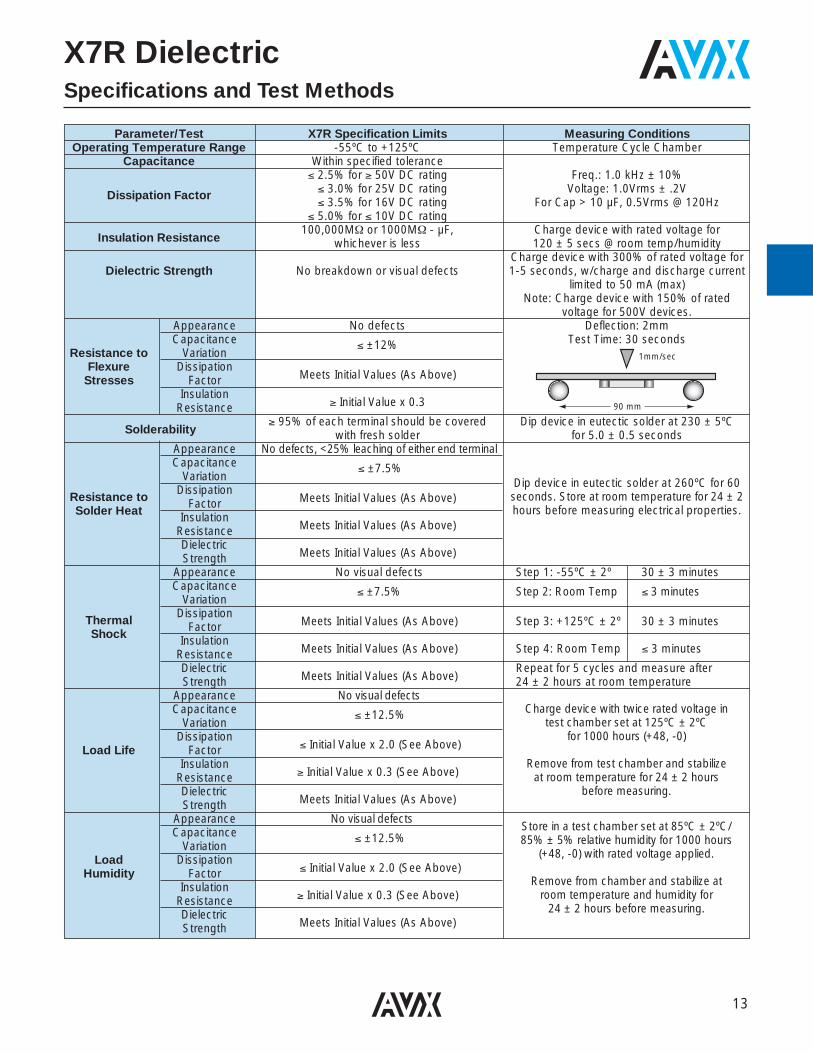
13
X7R DielectricSpecifications and Test Methods
Parameter/Test X7R Specification Limits Measuring ConditionsOperating Temperature Range -55ºC to +125ºC Temperature Cycle Chamber
Capacitance Within specified tolerance≤ 2.5% for ≥ 50V DC rating Freq.: 1.0 kHz ± 10%
Dissipation Factor ≤ 3.0% for 25V DC rating Voltage: 1.0Vrms ± .2V≤ 3.5% for 16V DC rating For Cap > 10 µF, 0.5Vrms @ 120Hz
≤ 5.0% for ≤ 10V DC rating
Insulation Resistance100,000MΩ or 1000MΩ - µF, Charge device with rated voltage for
whichever is less 120 ± 5 secs @ room temp/humidityCharge device with 300% of rated voltage for
Dielectric Strength No breakdown or visual defects 1-5 seconds, w/charge and discharge currentlimited to 50 mA (max)
Note: Charge device with 150% of ratedvoltage for 500V devices.
Appearance No defects Deflection: 2mmCapacitance Test Time: 30 seconds
Resistance to Variation≤ ±12%
Flexure DissipationMeets Initial Values (As Above)Stresses Factor
Insulation≥ Initial Value x 0.3Resistance
Solderability≥ 95% of each terminal should be covered Dip device in eutectic solder at 230 ± 5ºC
with fresh solder for 5.0 ± 0.5 secondsAppearance No defects, <25% leaching of either end terminalCapacitance
Variation≤ ±7.5%
Dip device in eutectic solder at 260ºC for 60DissipationMeets Initial Values (As Above) seconds. Store at room temperature for 24 ± 2Resistance to Factor hours before measuring electrical properties.Solder Heat InsulationMeets Initial Values (As Above)Resistance
Dielectric Meets Initial Values (As Above)Strength
Appearance No visual defects Step 1: -55ºC ± 2º 30 ± 3 minutesCapacitance
Variation≤ ±7.5% Step 2: Room Temp ≤ 3 minutes
DissipationMeets Initial Values (As Above) Step 3: +125ºC ± 2º 30 ± 3 minutesThermal FactorShock InsulationMeets Initial Values (As Above) Step 4: Room Temp ≤ 3 minutesResistance
Dielectric Meets Initial Values (As Above)
Repeat for 5 cycles and measure afterStrength 24 ± 2 hours at room temperature
Appearance No visual defectsCapacitance
Variation≤ ±12.5%
Dissipation≤ Initial Value x 2.0 (See Above)Load Life Factor
Insulation≥ Initial Value x 0.3 (See Above)Resistance
Dielectric Meets Initial Values (As Above)Strength
Appearance No visual defectsCapacitance
Variation≤ ±12.5%
Load Dissipation≤ Initial Value x 2.0 (See Above)Humidity Factor
Insulation≥ Initial Value x 0.3 (See Above)Resistance
Dielectric Meets Initial Values (As Above)Strength
Charge device with twice rated voltage intest chamber set at 125ºC ± 2ºC
for 1000 hours (+48, -0)
Remove from test chamber and stabilize at room temperature for 24 ± 2 hours
before measuring.
Store in a test chamber set at 85ºC ± 2ºC/85% ± 5% relative humidity for 1000 hours
(+48, -0) with rated voltage applied.
Remove from chamber and stabilize atroom temperature and humidity for
24 ± 2 hours before measuring.
1mm/sec
90 mm

14
X7R DielectricCapacitance Range
PREFERRED SIZES ARE SHADED
SIZE 0201 0402 0603 0805 1206Soldering Reflow Only Reflow Only Reflow Only Reflow/Wave Reflow/WavePackaging All Paper All Paper All Paper Paper/Embossed Paper/Embossed
(L) Length MM 0.60 ± 0.03 1.00 ± 0.10 1.60 ± 0.15 2.01 ± 0.20 3.20 ± 0.20 (in.) (0.024 ± 0.001) (0.040 ± 0.004) (0.063 ± 0.006) (0.079 ± 0.008) (0.126 ± 0.008)
(W) Width MM 0.30 ± 0.03 0.50 ± 0.10 0.81 ± 0.15 1.25 ± 0.20 1.60 ± 0.20(in.) (0.011 ± 0.001) (0.020 ± 0.004) (0.032 ± 0.006) (0.049 ± 0.008) (0.063 ± 0.008)
(t) Terminal MM 0.15 ± 0.05 0.25 ± 0.15 0.35 ± 0.15 0.50 ± 0.25 0.50 ± 0.25(in.) (0.006 ± 0.002) (0.010 ± 0.006) (0.014 ± 0.006) (0.020 ± 0.010) (0.020 ± 0.010)
WVDC 16 16 25 50 10 16 25 50 100 10 16 25 50 100 200 10 16 25 50 100 200 500Cap 100 A(pF) 150 A
220 A C330 A C G G J J J J J J K470 A C G G J J J J J J K680 A C G G J J J J J J K
1000 A C G G J J J J J J K1500 C G G J J J J J J J J J J J J M2200 C G G J J J J J J J J J J J J M3300 C C G G J J J J J J J J J J J J M4700 C G J J J J J J J J J J J J M6800 C C G J J J J J J J J J J J J P
Cap 0.010 C G J J J J J J J J J J J J P(µF 0.015 C G G J J J J J J J J J J J M
0.022 C G J J J J J M J J J J J M0.033 G J J J J M J J J J J M0.047 G G J J J J M J J J J J M0.068 G J J J J J J J J J P0.10 G G G J J J J J J J J M0.15 G J J J J J J J0.22 G J J M J J J J0.33 M M J J M M0.47 N M M M M0.68 N M M1.0 N M M Q1.5 P2.2 Q3.34.7102247
100WVDC 16 16 25 50 10 16 25 50 100 10 16 25 50 100 200 10 16 25 50 100 200 500
SIZE 0201 0402 0603 0805 1206
L
W
T
t
Letter A C E G J K M N P Q X Y ZMax. 0.33 0.56 0.71 0.86 0.94 1.02 1.27 1.40 1.52 1.78 2.29 2.54 2.79
Thickness (0.013) (0.022) (0.028) (0.034) (0.037) (0.040) (0.050) (0.055) (0.060) (0.070) (0.090) (0.100) (0.110)PAPER EMBOSSED

15
X7R DielectricCapacitance Range
Letter A C E G J K M N P Q X Y ZMax. 0.33 0.56 0.71 0.86 0.94 1.02 1.27 1.40 1.52 1.78 2.29 2.54 2.79
Thickness (0.013) (0.022) (0.028) (0.034) (0.037) (0.040) (0.050) (0.055) (0.060) (0.070) (0.090) (0.100) (0.110)PAPER EMBOSSED
PREFERRED SIZES ARE SHADED
SIZE 1210 1812 1825 2220 2225Soldering Reflow Only Reflow Only Reflow Only Reflow Only Reflow OnlyPackaging Paper/Embossed All Embossed All Embossed All Embossed All Embossed
(L) Length MM 3.20 ± 0.20 4.50 ± 0.30 4.50 ± 0.30 5.70 ± 0.40 5.72 ± 0.25(in.) (0.126 ± 0.008) (0.177 ± 0.012) (0.177 ± 0.012) (0.225 ± 0.016) (0.225 ± 0.010)
(W) Width MM 2.50 ± 0.20 3.20 ± 0.20 6.40 ± 0.40 5.00 ± 0.40 6.35 ± 0.25(in.) (0.098 ± 0.008) (0.126 ± 0.008) (0.252 ± 0.016) (0.197 ± 0.016) (0.250 ± 0.010)
(t) Terminal MM 0.50 ± 0.25 0.61 ± 0.36 0.61 ± 0.36 0.64 ± 0.39 0.64 ± 0.39(in.) (0.020 ± 0.010) (0.024 ± 0.014) (0.024 ± 0.014) (0.025 ± 0.015) (0.025 ± 0.015)
WVDC 10 16 25 50 100 200 500 50 100 200 500 50 100 6.3 50 100 200 50 100Cap 100(pF) 150
220330470680
10001500 J J J J J J M2200 J J J J J J M3300 J J J J J J M4700 J J J J J J M6800 J J J J J J M
Cap 0.010 J J J J J J M K K K K M M X X X X M P(µF 0.015 J J J J J J P K K K P M M X X X X M P
0.022 J J J J J J Q K K K P M M X X X X M P0.033 J J J J J J K K K X M M X X X X M P0.047 J J J J J J K K K Z M M X X X X M P0.068 J J J J J M K K K M M X X X X M P0.10 J J J J J M K K K M M X X X X M P0.15 J J J J M K K P M M X X X X M P0.22 J J J J P K K P M M X X X M P0.33 J J J J Z K M M M X X X M P0.47 M M M M Z K P M M X X X M P0.68 M M P X Z M Q M X X X M P1.0 N N P X Z M X M Z M P1.5 N N M M X2.2 X Z M3.34.7 Q Z10 Z2247
100WVDC 10 16 25 50 100 200 500 50 100 200 500 50 100 6.3 50 100 200 50 100
SIZE 1210 1812 1825 2220 2225
L
W
T
t

60
Packaging of Chip ComponentsAutomatic Insertion Packaging
TAPE & REEL QUANTITIESAll tape and reel specifications are in compliance with RS481.
8mm 12mm
Paper or Embossed Carrier 0612, 0508, 0805, 1206,1210
Embossed Only 1812, 18251808 2220, 2225
Paper Only 0201, 0306, 0402, 0603
Qty. per Reel/7" Reel 2,000, 3,000 or 4,000, 10,000, 15,000 3,000 500, 1,000Contact factory for exact quantity Contact factory for exact quantity
Qty. per Reel/13" Reel 5,000, 10,000, 50,000 10,000 4,000Contact factory for exact quantity
REEL DIMENSIONS
Tape A B* C D* N W1W2 W3Size(1) Max. Min. Min. Min. Max.
7.90 Min.8mm 14.4 (0.311)
(0.567) 10.9 Max.330 1.5 20.2 50.0 (0.429)
(12.992) (0.059) (0.795) (1.969) 11.9 Min.12mm 18.4 (0.469)
(0.724) 15.4 Max.(0.607)
Metric dimensions will govern.English measurements rounded and for reference only.(1) For tape sizes 16mm and 24mm (used with chip size 3640) consult EIA RS-481 latest revision.
13.0 +0.50-0.20
(0.512 +0.020)-0.008
8.40 +1.5-0.0
(0.331 +0.059 )-0.0
12.4 +2.0-0.0
(0.488 +0.079 )-0.0

61
Tape Size B1 D1 E2 F P1 R T2 W A0 B0 K0Max. Min. Min. Min. Max.
See Note 5 See Note 2
8mm4.35 1.00 6.25 3.50 ± 0.05 4.00 ± 0.10 25.0 2.50 Max. 8.30
See Note 1(0.171) (0.039) (0.246) (0.138 ± 0.002) (0.157 ± 0.004) (0.984) (0.098) (0.327)
12mm8.20 1.50 10.25 5.50 ± 0.05 4.00 ± 0.10 30.0 6.50 Max. 12.3
See Note 1(0.323) (0.059) (0.404) (0.217 ± 0.002) (0.157 ± 0.004) (1.181) (0.256) (0.484)
8mm 4.35 1.00 6.25 3.50 ± 0.05 2.00 ± 0.10 25.0 2.50 Max. 8.30See Note 11/2 Pitch (0.171) (0.039) (0.246) (0.138 ± 0.002) (0.079 ± 0.004) (0.984) (0.098) (0.327)
12mm 8.20 1.50 10.25 5.50 ± 0.05 8.00 ± 0.10 30.0 6.50 Max. 12.3 See Note 1Double (0.323) (0.059) (0.404) (0.217 ± 0.002) (0.315 ± 0.004) (1.181) (0.256) (0.484)Pitch
Embossed Carrier Configuration8 & 12mm Tape Only
P0
B0
P1
P2D0T2
T
TOP COVERTAPE
DEFORMATIONBETWEEN EMBOSSMENTS
CENTER LINESOF CAVITY MAX. CAVITY
SIZE - SEE NOTE 1
D1 FOR COMPONENTS2.00 mm x 1.20 mm ANDLARGER (0.079 x 0.047)
10 PITCHES CUMULATIVE TOLERANCE ON TAPE±0.2mm (±0.008)
B1
E1
F
EMBOSSMENT
User Direction of Feed
E2W
K0
T1S1
A0
B1 IS FOR TAPE READER REFERENCE ONLYINCLUDING DRAFT CONCENTRIC AROUND B0
8 & 12mm Embossed TapeMetric Dimensions Will GovernCONSTANT DIMENSIONS
VARIABLE DIMENSIONS
NOTES:1. The cavity defined by A0, B0, and K0 shall be configured to provide the following:
Surround the component with sufficient clearance such that:a) the component does not protrude beyond the sealing plane of the cover tape.b) the component can be removed from the cavity in a vertical direction without mechanical
restriction, after the cover tape has been removed.c) rotation of the component is limited to 20º maximum (see Sketches D & E).d) lateral movement of the component is restricted to 0.5mm maximum (see Sketch F).
2. Tape with or without components shall pass around radius “R” without damage.
3. Bar code labeling (if required) shall be on the side of the reel opposite the round sprocket holes.Refer to EIA-556.
4. B1 dimension is a reference dimension for tape feeder clearance only.
5. If P1 = 2.0mm, the tape may not properly index in all tape feeders.
Tape Size D0 E P0 P2 S1 Min. T Max. T1
8mm 1.75 ± 0.10 4.0 ± 0.10 2.0 ± 0.05 0.60 0.60 0.10and (0.069 ± 0.004) (0.157 ± 0.004) (0.079 ± 0.002) (0.024) (0.024) (0.004)
12mm Max.
0.50mm (0.020)Maximum
0.50mm (0.020)Maximum
Top View, Sketch "F"Component Lateral Movements
1.50 +0.10-0.0
(0.059 +0.004 )-0.0
Chip Orientation

62
Tape Size P1 E2 Min. F W A0 B0 TSee Note 4
8mm 4.00 ± 0.10 6.25 3.50 ± 0.05 See Note 1(0.157 ± 0.004) (0.246) (0.138 ± 0.002)
12mm 4.00 ± 0.010 10.25 5.50 ± 0.05 12.0 ± 0.30(0.157 ± 0.004) (0.404) (0.217 ± 0.002) (0.472 ± 0.012)
8mm 2.00 ± 0.05 6.25 3.50 ± 0.051/2 Pitch (0.079 ± 0.002) (0.246) (0.138 ± 0.002)
12mm 8.00 ± 0.10 10.25 5.50 ± 0.05 12.0 ± 0.30Double (0.315 ± 0.004) (0.404) (0.217 ± 0.002) (0.472 ± 0.012)Pitch
Paper Carrier Configuration8 & 12mm Tape Only
P0
B0
P1
P2D0T
TOP COVERTAPE
BOTTOM COVERTAPE
CENTER LINESOF CAVITY
CAVITY SIZESEE NOTE 1
10 PITCHES CUMULATIVE TOLERANCE ON TAPE±0.20mm (±0.008)
E1
F
G
User Direction of Feed
E2W
T1
T1 A0
8 & 12mm Paper TapeMetric Dimensions Will GovernCONSTANT DIMENSIONS
Tape Size D0 E P0 P2 T1 G. Min. R Min.
8mm 1.75 ± 0.10 4.00 ± 0.10 2.00 ± 0.05 0.10 0.75 25.0 (0.984)and (0.069 ± 0.004) (0.157 ± 0.004) (0.079 ± 0.002) (0.004) (0.030) See Note 2
12mm Max. Min. Min.
VARIABLE DIMENSIONS
1.10mm (0.043) Max.
for Paper BaseTape and
1.60mm (0.063) Max.
for Non-PaperBase Compositions
NOTES:1. The cavity defined by A0, B0, and T shall be configured to provide sufficient clearance
surrounding the component so that:a) the component does not protrude beyond either surface of the carrier tape;b) the component can be removed from the cavity in a vertical direction without
mechanical restriction after the top cover tape has been removed;c) rotation of the component is limited to 20º maximum (see Sketches A & B);d) lateral movement of the component is restricted to 0.5mm maximum
(see Sketch C).
2. Tape with or without components shall pass around radius “R” without damage.
3. Bar code labeling (if required) shall be on the side of the reel opposite the sprocketholes. Refer to EIA-556.
4. If P1 = 2.0mm, the tape may not properly index in all tape feeders.
0.50mm (0.020)Maximum
0.50mm (0.020)Maximum
Top View, Sketch "C"Component Lateral
1.50 +0.10-0.0
(0.059 +0.004 )-0.0
8.00 +0.30-0.10
(0.315 +0.012 )-0.004
8.00 +0.30-0.10
(0.315 +0.012 )-0.004
Bar Code Labeling StandardAVX bar code labeling is available and follows latest version of EIA-556

63
Bulk Case Packaging
CASE QUANTITIESPart Size 0402 0603 0805 1206
Qty. 10,000 (T=.023") 5,000 (T=.023")(pcs / cassette) 80,000 15,000 8,000 (T=.031") 4,000 (T=.032")
6,000 (T=.043") 3,000 (T=.044")
BENEFITS BULK FEEDER• Easier handling
• Smaller packaging volume(1/20 of T/R packaging)
• Easier inventory control
• Flexibility
• Recyclable
CASE DIMENSIONS
ShutterSlider
Attachment Base
110mm
12mm
36mm
Case
Cassette
Gate
Shooter
Chips
Expanded DrawingMounter
Head
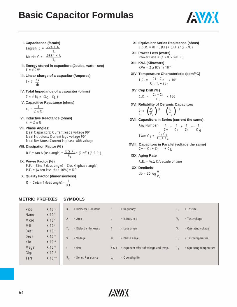
64
I. Capacitance (farads)
English: C = .224 K A TD
Metric: C = .0884 K ATD
II. Energy stored in capacitors (Joules, watt - sec)E = 1⁄2 CV2
III. Linear charge of a capacitor (Amperes)
I = C dVdt
IV. Total Impedance of a capacitor (ohms)
Z = R2S + (XC - XL )2
V. Capacitive Reactance (ohms)
xc = 12 π fC
VI. Inductive Reactance (ohms)xL = 2 π fL
VII. Phase Angles:Ideal Capacitors: Current leads voltage 90°Ideal Inductors: Current lags voltage 90°Ideal Resistors: Current in phase with voltage
VIII. Dissipation Factor (%)
D.F.= tan (loss angle) = E.S.R. = (2 πfC) (E.S.R.)Xc
IX. Power Factor (%)P.F. = Sine (loss angle) = Cos f (phase angle)P.F. = (when less than 10%) = DF
X. Quality Factor (dimensionless)
Q = Cotan (loss angle) = 1D.F.
XI. Equivalent Series Resistance (ohms)E.S.R. = (D.F.) (Xc) = (D.F.) / (2 π fC)
XII. Power Loss (watts)Power Loss = (2 π fCV2) (D.F.)
XIII. KVA (Kilowatts)KVA = 2 π fCV2 x 10 -3
XIV. Temperature Characteristic (ppm/°C)
T.C. = Ct – C25 x 106
C25 (Tt – 25)
XV. Cap Drift (%)
C.D. = C1 – C2 x 100C1
XVI. Reliability of Ceramic CapacitorsL0 = Vt X Tt YLt
( Vo ) ( To
)XVII. Capacitors in Series (current the same)
Any Number: 1 = 1 + 1 --- 1 CT C1 C2 CN
C1 C2Two: CT =C1 + C2
XVIII. Capacitors in Parallel (voltage the same)CT = C1 + C2 --- + CN
XIX. Aging Rate
A.R. = %D C/decade of time
XX. Decibels
db = 20 log V1
V2
Pico X 10-12
Nano X 10-9
Micro X 10-6
Milli X 10-3
Deci X 10-1
Deca X 10+1
Kilo X 10+3
Mega X 10+6
Giga X 10+9
Tera X 10+12
K = Dielectric Constant f = frequency Lt = Test life
A = Area L = Inductance Vt = Test voltage
TD = Dielectric thickness = Loss angle Vo = Operating voltage
V = Voltage f = Phase angle Tt = Test temperature
t = time X & Y = exponent effect of voltage and temp. To = Operating temperature
Rs = Series Resistance Lo = Operating life
METRIC PREFIXES SYMBOLS
Basic Capacitor Formulas

65
General Description
Formulations – Multilayer ceramic capacitors are availablein both Class 1 and Class 2 formulations. Temperaturecompensating formulation are Class 1 and temperature stable and general application formulations are classified as Class 2.
Class 1 – Class 1 capacitors or temperature compensatingcapacitors are usually made from mixtures of titanateswhere barium titanate is normally not a major part of themix. They have predictable temperature coefficients and in general, do not have an aging characteristic. Thus theyare the most stable capacitor available. The most popularClass 1 multilayer ceramic capacitors are C0G (NP0) temperature compensating capacitors (negative-positive 0 ppm/°C).
Class 2 – EIA Class 2 capacitors typically are based on thechemistry of barium titanate and provide a wide range ofcapacitance values and temperature stability. The mostcommonly used Class 2 dielectrics are X7R and Y5V. TheX7R provides intermediate capacitance values which varyonly ±15% over the temperature range of -55°C to 125°C. Itfinds applications where stability over a wide temperaturerange is required.The Y5V provides the highest capacitance values and isused in applications where limited temperature changes areexpected. The capacitance value for Y5V can vary from22% to -82% over the -30°C to 85°C temperature range.All Class 2 capacitors vary in capacitance value under theinfluence of temperature, operating voltage (both AC andDC), and frequency. For additional information on perfor-mance changes with operating conditions, consult AVX’ssoftware, SpiCap.
Basic Construction – A multilayer ceramic (MLC) capaci-tor is a monolithic block of ceramic containing two sets ofoffset, interleaved planar electrodes that extend to twoopposite surfaces of the ceramic dielectric. This simple
structure requires a considerable amount of sophistication,both in material and manufacture, to produce it in the qualityand quantities needed in today’s electronic equipment.
Ceramic LayerElectrode
TerminatedEdge
TerminatedEdge
End Terminations
Margin Electrodes
Multilayer Ceramic Capacitor
Figure 1

66
In specifying capacitance change with temperature for Class2 materials, EIA expresses the capacitance change over anoperating temperature range by a 3 symbol code. The firstsymbol represents the cold temperature end of the temper-ature range, the second represents the upper limit of theoperating temperature range and the third symbol repre-sents the capacitance change al lowed over the operating temperature range. Table 1 provides a detailedexplanation of the EIA system.
Effects of Voltage – Variations in voltage have little effecton Class 1 dielectric but does affect the capacitance anddissipation factor of Class 2 dielectrics. The application ofDC voltage reduces both the capacitance and dissipationfactor while the application of an AC voltage within a reasonable range tends to increase both capacitance anddissipation factor readings. If a high enough AC voltage isapplied, eventually it will reduce capacitance just as a DCvoltage will. Figure 2 shows the effects of AC voltage.
Capacitor specifications specify the AC voltage at which tomeasure (normally 0.5 or 1 VAC) and application of thewrong voltage can cause spurious readings. Figure 3 givesthe voltage coefficient of dissipation factor for various ACvoltages at 1 kilohertz. Applications of different frequencieswill affect the percentage changes versus voltages.
Typical effect of the application of DC voltage is shown inFigure 4. The voltage coefficient is more pronounced forhigher K dielectrics. These figures are shown for room tem-perature conditions. The combination characteristic knownas voltage temperature limits which shows the effects ofrated voltage over the operating temperature range isshown in Figure 5 for the military BX characteristic.
General Description
Figure 2
50
40
30
20
10
012.5 25 37.5 50
Volts AC at 1.0 KHz
Cap
acita
nce
Cha
nge
Per
cent
Cap. Change vs. A.C. VoltsX7R
Figure 3
Curve 3 - 25 VDC Rated CapacitorCurve 2 - 50 VDC Rated CapacitorCurve 1 - 100 VDC Rated Capacitor Curve 3
Curve 2
Curve 1
.5 1.0 1.5 2.0 2.5AC Measurement Volts at 1.0 KHz
Dis
sip
atio
n Fa
ctor
Per
cent
10.0
8.0
6.0
4.0
2.0
0
D.F. vs. A.C. Measurement VoltsX7R
EIA CODEPercent Capacity Change Over Temperature Range
RS198 Temperature Range
X7 -55°C to +125°CX6 -55°C to +105°CX5 -55°C to +85°CY5 -30°C to +85°CZ5 +10°C to +85°C
Code Percent Capacity Change
D ±3.3%E ±4.7%F ±7.5%P ±10%R ±15%S ±22%T +22%, -33%U +22%, - 56%V +22%, -82%
MIL CODE
Symbol Temperature Range
A -55°C to +85°CB -55°C to +125°CC -55°C to +150°C
Symbol Cap. Change Cap. ChangeZero Volts Rated Volts
R +15%, -15% +15%, -40%S +22%, -22% +22%, -56%W +22%, -56% +22%, -66%X +15%, -15% +15%, -25%Y +30%, -70% +30%, -80%Z +20%, -20% +20%, -30%
Table 1: EIA and MIL Temperature Stable and GeneralApplication Codes
EXAMPLE – A capacitor is desired with the capacitance value at 25°Cto increase no more than 7.5% or decrease no more than 7.5% from -30°C to +85°C. EIA Code will be Y5F.
Temperature characteristic is specified by combining range andchange symbols, for example BR or AW. Specification slash sheetsindicate the characteristic applicable to a given style of capacitor.

67
General Description
Typical Cap. Change vs. D.C. VoltsX7R
Typical Cap. Change vs. TemperatureX7R
Effects of Time – Class 2 ceramic capacitors changecapacitance and dissipation factor with time as well as tem-perature, voltage and frequency. This change with time isknown as aging. Aging is caused by a gradual re-alignmentof the crystalline structure of the ceramic and produces anexponential loss in capacitance and decrease in dissipationfactor versus time. A typical curve of aging rate for semi-stable ceramics is shown in Figure 6.If a Class 2 ceramic capacitor that has been sitting on theshelf for a period of time, is heated above its curie point,(125°C for 4 hours or 150°C for 1⁄2 hour will suffice) the partwill de-age and return to its initial capacitance and dissi-pation factor readings. Because the capacitance changes rapidly, immediately after de-aging, the basic capacitance measurements are normally referred to a time period some-time after the de-aging process. Various manufacturers usedifferent time bases but the most popular one is one day or twenty-four hours after “last heat.” Change in the agingcurve can be caused by the application of voltage and other stresses. The possible changes in capacitance due tode-aging by heating the unit explain why capacitancechanges are allowed after test, such as temperature cycling,moisture resistance, etc., in MIL specs. The application ofhigh voltages such as dielectric withstanding voltages also
tends to de-age capacitors and is why re-reading of capaci-tance after 12 or 24 hours is allowed in military specifica-tions after dielectric strength tests have been performed.
Effects of Frequency – Frequency affects capacitanceand impedance characteristics of capacitors. This effect ismuch more pronounced in high dielectric constant ceramicformulation than in low K formulations. AVX’s SpiCap soft-ware generates impedance, ESR, series inductance, seriesresonant frequency and capacitance all as functions of frequency, temperature and DC bias for standard chip sizesand styles. It is available free from AVX and can be down-loaded for free from AVX website: www.avx.com.
25% 50% 75% 100%
Percent Rated Volts
Cap
acita
nce
Cha
nge
Per
cent 2.5
0
-2.5
-5
-7.5
-10
0VDC
-55 -35 -15 +5 +25 +45 +65 +85 +105 +125
Temperature Degrees Centigrade
Cap
acita
nce
Cha
nge
Per
cent
+20
+10
0
-10
-20
-30
Figure 4
Figure 5
1 10 100 1000 10,000 100,000 Hours
Cap
acita
nce
Cha
nge
Per
cent
+1.5
0
-1.5
-3.0
-4.5
-6.0
-7.5
Characteristic Max. Aging Rate %/Decade C0G (NP0)X7R, X5RY5V
None27
Figure 6
Typical Curve of Aging RateX7R

68
Effects of Mechanical Stress – High “K” dielectricceramic capacitors exhibit some low level piezoelectricreactions under mechanical stress. As a general statement,the piezoelectric output is higher, the higher the dielectricconstant of the ceramic. It is desirable to investigate thiseffect before using high “K” dielectrics as coupling capaci-tors in extremely low level applications.Reliability – Historically ceramic capacitors have been oneof the most reliable types of capacitors in use today. The approximate formula for the reliability of a ceramiccapacitor is:
Lo = Vt X Tt Y
Lt Vo To
whereLo = operating life Tt = test temperature andLt = test life To = operating temperatureVt = test voltage in °CVo = operating voltage X,Y = see text
Historically for ceramic capacitors exponent X has beenconsidered as 3. The exponent Y for temperature effectstypically tends to run about 8.
A capacitor is a component which is capable of storingelectrical energy. It consists of two conductive plates (elec-trodes) separated by insulating material which is called thedielectric. A typical formula for determining capacitance is:
C = .224 KAt
C = capacitance (picofarads)K = dielectric constant (Vacuum = 1)A = area in square inchest = separation between the plates in inches
(thickness of dielectric).224 = conversion constant
(.0884 for metric system in cm)Capacitance – The standard unit of capacitance is thefarad. A capacitor has a capacitance of 1 farad when 1coulomb charges it to 1 volt. One farad is a very large unitand most capacitors have values in the micro (10-6), nano(10-9) or pico (10-12) farad level.Dielectric Constant – In the formula for capacitance givenabove the dielectric constant of a vacuum is arbitrarily cho-sen as the number 1. Dielectric constants of other materialsare then compared to the dielectric constant of a vacuum.Dielectric Thickness – Capacitance is indirectly propor-tional to the separation between electrodes. Lower voltagerequirements mean thinner dielectrics and greater capaci-tance per volume.Area – Capacitance is directly proportional to the area ofthe electrodes. Since the other variables in the equation areusually set by the performance desired, area is the easiestparameter to modify to obtain a specific capacitance withina material group.
Energy Stored – The energy which can be stored in acapacitor is given by the formula:
E = 1⁄2CV2
E = energy in joules (watts-sec)V = applied voltageC = capacitance in farads
Potential Change – A capacitor is a reactive componentwhich reacts against a change in potential across it. This isshown by the equation for the linear charge of a capacitor:
I ideal = C dVdt
whereI = Current
C = CapacitancedV/dt = Slope of voltage transition across capacitor
Thus an infinite current would be required to instantlychange the potential across a capacitor. The amount ofcurrent a capacitor can “sink” is determined by the aboveequation.Equivalent Circuit – A capacitor, as a practical device,exhibits not only capacitance but also resistance andinductance. A simplified schematic for the equivalent circuitis:
C = Capacitance L = Inductance Rs = Series Resistance Rp = Parallel Resistance
Reactance – Since the insulation resistance (Rp) is normal-ly very high, the total impedance of a capacitor is:
Z = R2S + (XC - XL)2
whereZ = Total Impedance Rs = Series ResistanceXC = Capacitive Reactance = 1
2 π fCXL = Inductive Reactance = 2 π fL
The variation of a capacitor’s impedance with frequencydetermines its effectiveness in many applications.Phase Angle – Power Factor and Dissipation Factor areoften confused since they are both measures of the loss ina capacitor under AC application and are often almostidentical in value. In a “perfect” capacitor the current in thecapacitor will lead the voltage by 90°.
General Description
R
L R
C
P
S

69
General Description
In practice the current leads the voltage by some otherphase angle due to the series resistance RS. The comple-ment of this angle is called the loss angle and:
Power Factor (P.F.) = Cos f or Sine Dissipation Factor (D.F.) = tan
for small values of the tan and sine are essentially equalwhich has led to the common interchangeability of the twoterms in the industry.
Equivalent Series Resistance – The term E.S.R. orEquivalent Series Resistance combines all losses bothseries and parallel in a capacitor at a given frequency sothat the equivalent circuit is reduced to a simple R-C seriesconnection.
Dissipation Factor – The DF/PF of a capacitor tells whatpercent of the apparent power input will turn to heat in thecapacitor.
Dissipation Factor = E.S.R. = (2 π fC) (E.S.R.)XC
The watts loss are:Watts loss = (2 π fCV2) (D.F.)
Very low values of dissipation factor are expressed as theirreciprocal for convenience. These are called the “Q” orQuality factor of capacitors.Parasitic Inductance – The parasitic inductance of capac-itors is becoming more and more important in the decou-pling of today’s high speed digital systems. The relationshipbetween the inductance and the ripple voltage induced onthe DC voltage line can be seen from the simple inductanceequation:
V = L di dt
The seen in current microprocessors can be as high as0.3 A/ns, and up to 10A/ns. At 0.3 A/ns, 100pH of parasiticinductance can cause a voltage spike of 30mV. While thisdoes not sound very drastic, with the Vcc for microproces-sors decreasing at the current rate, this can be a fairly largepercentage.Another important, often overlooked, reason for knowingthe parasitic inductance is the calculation of the resonantfrequency. This can be important for high frequency, by-pass capacitors, as the resonant point will give the mostsignal attenuation. The resonant frequency is calculatedfrom the simple equation:
fres = 1
2 LCInsulation Resistance – Insulation Resistance is the resistance measured across the terminals of a capacitorand consists principally of the parallel resistance RP shownin the equivalent circuit. As capacitance values and hencethe area of dielectric increases, the I.R. decreases andhence the product (C x IR or RC) is often specified in ohmfaradsor more commonly megohm-microfarads. Leakagecurrent is determined by dividing the rated voltage by IR(Ohm’s Law).Dielectric Strength – Dielectric Strength is an expressionof the ability of a material to withstand an electrical stress.Although dielectric strength is ordinarily expressed in volts, itis actually dependent on the thickness of the dielectric andthus is also more generically a function of volts/mil.Dielectric Absorption – A capacitor does not dischargeinstantaneously upon application of a short circuit, butdrains gradually after the capacitance proper has been dis-charged. It is common practice to measure the dielectricabsorption by determining the “reappearing voltage” whichappears across a capacitor at some point in time after it hasbeen fully discharged under short circuit conditions.Corona – Corona is the ionization of air or other vaporswhich causes them to conduct current. It is especiallyprevalent in high voltage units but can occur with low voltagesas well where high voltage gradients occur. The energydischarged degrades the performance of the capacitor andcan in time cause catastrophic failures.
di dt
I (Ideal)I (Actual)
PhaseAngle
LossAngle
VIRs
f
E.S.R. C

70
Surface Mounting GuideMLC Chip Capacitors
Component pads should be designed to achieve good solder filets and minimize component movement duringreflow soldering. Pad designs are given below for the mostcommon sizes of multilayer ceramic capacitors for bothwave and reflow soldering. The basis of these designs is:
• Pad width equal to component width. It is permissible todecrease this to as low as 85% of component width but itis not advisable to go below this.
• Pad overlap 0.5mm beneath component.• Pad extension 0.5mm beyond components for reflow and
1.0mm for wave soldering.
D1
D2
D3
D4
D5
Case Size D1 D2 D3 D4 D50402 1.70 (0.07) 0.60 (0.02) 0.50 (0.02) 0.60 (0.02) 0.50 (0.02)0603 2.30 (0.09) 0.80 (0.03) 0.70 (0.03) 0.80 (0.03) 0.75 (0.03)0805 3.00 (0.12) 1.00 (0.04) 1.00 (0.04) 1.00 (0.04) 1.25 (0.05)1206 4.00 (0.16) 1.00 (0.04) 2.00 (0.09) 1.00 (0.04) 1.60 (0.06)1210 4.00 (0.16) 1.00 (0.04) 2.00 (0.09) 1.00 (0.04) 2.50 (0.10)1808 5.60 (0.22) 1.00 (0.04) 3.60 (0.14) 1.00 (0.04) 2.00 (0.08)1812 5.60 (0.22) 1.00 (0.04)) 3.60 (0.14) 1.00 (0.04) 3.00 (0.12)1825 5.60 (0.22) 1.00 (0.04) 3.60 (0.14) 1.00 (0.04) 6.35 (0.25)2220 6.60 (0.26) 1.00 (0.04) 4.60 (0.18) 1.00 (0.04) 5.00 (0.20)2225 6.60 (0.26) 1.00 (0.04) 4.60 (0.18) 1.00 (0.04) 6.35 (0.25)Dimensions in millimeters (inches)
REFLOW SOLDERING
WAVE SOLDERING
Component SpacingFor wave soldering components, must be spaced sufficientlyfar apart to avoid bridging or shadowing (inability of solderto penetrate properly into small spaces). This is less impor-tant for reflow soldering but sufficient space must beallowed to enable rework should it be required.
Preheat & SolderingThe rate of preheat should not exceed 4°C/second to prevent thermal shock. A better maximum figure is about2°C/second.For capacitors size 1206 and below, with a maximum thickness of 1.25mm, it is generally permissible to allow atemperature differential from preheat to soldering of 150°C.In all other cases this differential should not exceed 100°C.For further specific application or process advice, pleaseconsult AVX.CleaningCare should be taken to ensure that the capacitors arethoroughly cleaned of flux residues especially the spacebeneath the capacitor. Such residues may otherwisebecome conductive and effectively offer a low resistancebypass to the capacitor.Ultrasonic cleaning is permissible, the recommended conditions being 8 Watts/litre at 20-45 kHz, with a processcycle of 2 minutes vapor rinse, 2 minutes immersion in theultrasonic solvent bath and finally 2 minutes vapor rinse.
D1
D2
D3
D4
D5
Case Size D1 D2 D3 D4 D50603 3.10 (0.12) 1.20 (0.05) 0.70 (0.03) 1.20 (0.05) 0.75 (0.03)0805 4.00 (0.15) 1.50 (0.06) 1.00 (0.04) 1.50 (0.06) 1.25 (0.05)1206 5.00 (0.19) 1.50 (0.06) 2.00 (0.09) 1.50 (0.06) 1.60 (0.06)
Dimensions in millimeters (inches)
≥1mm (0.04)
≥1.5mm (0.06)
≥1mm (0.04)
Component Pad Design

71
Surface Mounting GuideMLC Chip Capacitors
APPLICATION NOTES
StorageGood solderability is maintained for at least twelve months,provided the components are stored in their “as received”packaging at less than 40°C and 70% RH.
SolderabilityTerminations to be well soldered after immersion in a 60/40tin/lead solder bath at 235 ± 5°C for 2 ± 1 seconds.
LeachingTerminations will resist leaching for at least the immersiontimes and conditions shown below.
Recommended Soldering Profiles
Lead-Free Reflow Profile
Lead-Free Wave SolderingThe recommended peak temperature for lead-free wave soldering is 250°C-260°C for 3-5 seconds. The other para-meters of the profile remains the same as above.The following should be noted by customers changing fromlead based systems to the new lead free pastes.a) The visual standards used for evaluation of solder joints
will need to be modified as lead free joints are not asbright as with tin-lead pastes and the fillet may not be aslarge.
b) Resin color may darken slightly due to the increase in temperature required for the new pastes.
c) Lead-free solder pastes do not allow the same self align-ment as lead containing systems. Standard mountingpads are acceptable, but machine set up may need to bemodified.
GeneralSurface mounting chip multilayer ceramic capacitors are designed for soldering to printed circuit boards or othersubstrates. The construction of the components is such thatthey will withstand the time/temperature profiles used in bothwave and reflow soldering methods.
HandlingChip multilayer ceramic capacitors should be handled withcare to avoid damage or contamination from perspirationand skin oils. The use of tweezers or vacuum pick ups is strongly recommended for individual components. Bulkhandling should ensure that abrasion and mechanical shockare minimized. Taped and reeled components provides theideal medium for direct presentation to the placementmachine. Any mechanical shock should be minimized duringhandling chip multilayer ceramic capacitors.
PreheatIt is important to avoid the possibility of thermal shock duringsoldering and carefully controlled preheat is thereforerequired. The rate of preheat should not exceed 4°C/second
Termination Type Solder Solder Immersion TimeTin/Lead/Silver Temp. °C Seconds
Nickel Barrier 60/40/0 260 ± 5 30 ± 1
Reflow
300
250
200
150
100
50
0
Sol
der
Tem
p.
10 sec. max1min1min
(Minimize soldering time)
NaturalCooling
220°Cto
250°C
Preheat
Wave
300
250
200
150
100
50
0
Sol
der
Tem
p.
(Preheat chips before soldering)T/maximum 150°C
3 sec. max1 to 2 min
PreheatNaturalCooling
230°Cto
250°C
T
3002502001501005000 50 100 150 200 250 300
• Pre-heating: 150°C ±15°C / 60-90s• Max. Peak Gradient 2.5°C/s• Peak Temperature: 245°C ±5°C• Time at >230°C: 40s Max.
Tem
per
atur
e °C
Time (s)

72
Surface Mounting GuideMLC Chip Capacitorsand a target figure 2°C/second is recommended. Althoughan 80°C to 120°C temperature differential is preferred,recent developments allow a temperature differentialbetween the component surface and the soldering temper-ature of 150°C (Maximum) for capacitors of 1210 size andbelow with a maximum thickness of 1.25mm. The user iscautioned that the risk of thermal shock increases as chipsize or temperature differential increases.
SolderingMildly activated rosin fluxes are preferred. The minimumamount of solder to give a good joint should be used.Excessive solder can lead to damage from the stressescaused by the difference in coefficients of expansionbetween solder, chip and substrate. AVX terminations aresuitable for all wave and reflow soldering systems. If handsoldering cannot be avoided, the preferred technique is theutilization of hot air soldering tools.
CoolingNatural cooling in air is preferred, as this minimizes stresseswithin the soldered joint. When forced air cooling is used,cooling rate should not exceed 4°C/second. Quenching is not recommended but if used, maximum temperature differentials should be observed according to the preheat conditions above.
CleaningFlux residues may be hygroscopic or acidic and must beremoved. AVX MLC capacitors are acceptable for use withall of the solvents described in the specifications MIL-STD-202 and EIA-RS-198. Alcohol based solvents are acceptableand properly controlled water cleaning systems are alsoacceptable. Many other solvents have been proven successful,and most solvents that are acceptable to other componentson circuit assemblies are equally acceptable for use withceramic capacitors.
POST SOLDER HANDLINGOnce SMP components are soldered to the board, anybending or flexure of the PCB applies stresses to the sol-dered joints of the components. For leaded devices, thestresses are absorbed by the compliancy of the metal leadsand generally don’t result in problems unless the stress islarge enough to fracture the soldered connection.Ceramic capacitors are more susceptible to such stressbecause they don’t have compliant leads and are brittle innature. The most frequent failure mode is low DC resistanceor short circuit. The second failure mode is significant lossof capacitance due to severing of contact between sets ofthe internal electrodes.Cracks caused by mechanical flexure are very easily identi-fied and generally take one of the following two generalforms:
Mechanical cracks are often hidden underneath the termi-nation and are difficult to see externally. However, if one endtermination falls off during the removal process from PCB,this is one indication that the cause of failure was excessivemechanical stress due to board warping.
Type A: Angled crack between bottom of device to top of solder joint.
Type B: Fracture from top of device to bottom of device.

73
Surface Mounting GuideMLC Chip Capacitors
PCB BOARD DESIGNTo avoid many of the handling problems, AVX recommends that MLCs be located at least .2" away from nearest edge ofboard. However when this is not possible, AVX recommends that the panel be routed along the cut line, adjacent to where theMLC is located.
Solder Tip Solder Tip
Preferred Method - No Direct Part Contact Poor Method - Direct Contact with Part
No Stress Relief for MLCs Routed Cut Line Relieves Stress on MLC
COMMON CAUSES OF MECHANICAL CRACKINGThe most common source for mechanical stress is boarddepanelization equipment, such as manual breakapart, v-cutters and shear presses. Improperly aligned or dull cuttersmay cause torqueing of the PCB resulting in flex stressesbeing transmitted to components near the board edge.Another common source of flexural stress is contact duringparametric testing when test points are probed. If the PCBis allowed to flex during the test cycle, nearby ceramiccapacitors may be broken.A third common source is board to board connections atvertical connectors where cables or other PCBs are con-nected to the PCB. If the board is not supported during theplug/unplug cycle, it may flex and cause damage to nearbycomponents.Special care should also be taken when handling large (>6"on a side) PCBs since they more easily flex or warp thansmaller boards.
REWORKING OF MLCsThermal shock is common in MLCs that are manuallyattached or reworked with a soldering iron. AVX stronglyrecommends that any reworking of MLCs be done with hotair reflow rather than soldering irons. It is practically impossi-ble to cause any thermal shock in ceramic capacitors whenusing hot air reflow.However direct contact by the soldering iron tip often caus-es thermal cracks that may fail at a later date. If rework bysoldering iron is absolutely necessary, it is recommendedthat the wattage of the iron be less than 30 watts and thetip temperature be <300ºC. Rework should be performedby applying the solder iron tip to the pad and not directlycontacting any part of the ceramic capacitor.

One Magnetics Pkwy, Gowanda, NY 14070 • (t) 716-532-2234 • (f) 716-532-2702 • [email protected] www.gowanda.com84
POWER INDUCTORS - THRU HOLE
CMF4 HLF RoHS Horizontal Mount Common Modes
PART INDUCTANCE DCR CURRENT LEAKAGE INTERWINDING A B C D E NUMBER @ 10 kHz OHMS RATING L CAPACITANCE DIM. DIM. DIM. DIM. DIM. µH ± 30%* MAX.* AMPS µH REF. pF REF. NOM. NOM. NOM. NOM. NOM.
CMF4-1003HLF 100 .0025 15.0 1.5 4.8 1.04(26.42) .440(11.18) .800(20.32) .300(7.62) .051(1.30)CMF4-2503HLF 250 .0038 12.0 3.2 8.0 1.04(26.42) .440(11.18) .800(20.32) .300(7.62) .051(1.30)CMF4-5003HLF 500 .006 10.0 5.8 9.7 1.04(26.42) .425(10.80) .800(20.32) .300(7.62) .045(1.14)CMF4-7503HLF 750 .013 6.7 8.0 12.0 1.00(25.40) .425(10.80) .800(20.32) .300(7.62) .036(0.91)CMF4-1004HLF 1000 .018 5.7 11.0 12.0 1.00(25.40) .400(10.16) .800(20.32) .300(7.62) .032(0.81)CMF4-1704HLF 1700 .060 3.1 22.0 11.0 .950(24.13) .370(9.40) .800(20.32) .300(7.62) .020(0.51)CMF4-2504HLF 2500 .073 2.8 29.0 15.0 .950(24.13) .370(9.40) .800(20.32) .300(7.62) .020(0.51)CMF4-3304HLF 3300 .125 2.2 38.0 15.0 .950(24.13) .370(9.40) .800(20.32) .300(7.62) .016(0.41)CMF4-5004HLF 5000 .150 2.0 48.0 17.0 .950(24.13) .370(9.40) .800(20.32) .300(7.62) .016(0.41)CMF4-7504HLF 7500 .300 1.4 80.0 20.0 .950(24.13) .370(9.40) .800(20.32) .300(7.62) .013(0.33)CMF4-1005HLF 10000 .390 1.2 95.0 20.0 .935(23.75) .370(9.40) .800(20.32) .300(7.62) .011(0.28)
SIDEVIEW
CMF4-XXXXHGOWANDA B
Edia.
CCENTERS
.500±.062(12.7±1.57)
BOTTOMVIEW
2
3
1
4
ADCENTERS
1
2 3
4
NOTES:
•InductanceandDCRisforeachsideorsinglewinding
•Operatingtemperature-55°Cto+125°C
PACKAGING SPECS:
Bulkonly.
in.(mm)


5mm LED Panel Mount Indicator 5V or 12V Integral Resistor.250” Mounting Hole, Snap In Mounting 559 Series
Dialight
Peak lv Vf Min Viewing DC Temperature °CPart Termination Wavelength Typical Volts If (mA) Reverse Angle Forward Number Color Options (nm) (mcd) (V) Typ Max Voltage 2Θ1/2 Voltage Operating Storage559-0102-00x R 1,3,7 655 2 5 13 20 5 60 7.5 -40/+85 -55/+100559-0103-00x R 1,3,7 655 2 12 13 20 5 60 15 -40/+85 -55/+100559-0202-00x G 1,3,7 565 8 5 12 15 5 60 7.5 -20/+85 -55/+100559-0203-00x G 1,3,7 565 4 12 13 20 5 60 15 -20/+85 -55/+100559-0302-00x Y 1,3,7 583 8 5 10 15 5 60 7.5 -40/+85 -55/+100559-0303-00x Y 1,3,7 583 8 12 13 20 5 60 15 -40/+85 -55/+100
Typical Operating Characteristics (TA=25°C) Absolute DIFFUSED LED Maximum Ratings
COLOR CODES:
R RedG GreenY Yellow
BENEFITS• Available with a variety of LEDs• Designed for quick positive insertions in panels from .787mm [.031] through 1.57mm [.062] thick. Recommended hole size from 6.32mm [.249] to 6.40mm [.252].
• Front panel mounting• Uniform illumination• Snap-in mounting requires no additional hardware• IC compatible• Housing meets UL94V-0• High reliability - 100,000 hour life• Black housing enhances LED contrast• Straight terminals suitable for wire-wrapping
CUSTOM CAPABILITIESConnectors and terminals can be added to wire leads
5 5 9 X X X X 0 0 X@@@@@@@@e?@@@@@@@@e?@@h?@@h?@@h?@@h?@@h?@@h?
@@@@@@@@e?@@@@@@@@?e@@@@@@@@e?@@@@@@@@?e@@@@@@@@e?@@@@@@@@?e@@@@@@@@e?@@@@@@@@e?@@@@@@@@?e@@@@@@@@e?@@@@@@@@?e@@@@@@@@e?@@@@@@@@?e@@@@@@@@e?
@@@@@@@@@@@@@@@@@@@@@@@@@@@@
@@@@@@@@@@@@@@@@
@@@@@@@@@@@@@@@@
?@@?@@?@@?@@?@@?@@
?@@@@@@@@?@@@@@@@@
?@@@@@@@@?e@@@@@@@@e?@@@@@@@@?e@@@@@@@@e?@@@@@@@@?e@@@@@@@@e?@@@@@@@@?@@@@@@@@?e@@@@@@@@e?@@@@@@@@?e@@@@@@@@e?@@@@@@@@?e@@@@@@@@e?@@@@@@@@
@@g@@g@@g@@g@@g@@g@@@@@@@@@@@@@@@@
@@@@@@@@@@@@@@@@
@@@@@@@@@@@@@@@@
Termination Option1 = Straight Terminals3 = 6” Wire Leads7 = 14” Wire Leads
PART NUMBER ORDERING CODE
Series
– –
7.41[.281]
15.88[.625] MAX
5.33[.210]MAX
7 . 6 2[ . 3 0 0 ]
M I N1.27
[.050]
.46/.69[.018/.02]
SQ.
3.18[.125]CATHODE
LEAD ( – )
12.70[.500]
1.47[.058]
3.18[.125]
355.60[14.0]
NOTE: WIRE LEAD COLORS RED (ANODE)& BLACK (CATHODE)
STRAIGHT TERMINALS – TERMINAL OPTION 1
24 AWG WIRE LEADS – TERMINAL OPTION 3 FOR 6”TERMINAL OPTION 7 FOR 14”
7.41[.281]
Dia l ight Corporat ion • 1501 State Route 34 • Farmingdale, NJ 07727 • TEL: (732) 919-3119 • FAX: (732) 751-5778 • www.d ia l ight .com
Example

2007-05-291
BCR401R
LED Driver • Supplies stable bias current even at low battery voltage
• Suitable for PWM control up to 100kHz• Ideal for stabilizing bias current of LEDs• Negative temperature coefficient protects LEDs against thermal overload
• Pb-free (RoHS compliant) package1)
• Qualified according AEC Q101
1
24
3
EHA07188
4 3
21
Type Marking Pin Configuration PackageBCR401R W5s 1 = GND 2 = Iout 3 = VS 4 = Rext SOT143R
Maximum RatingsParameter Symbol Value UnitSource voltage VS 18 V
Output current Iout 60 mAOutput voltage Vout 16 V
Reverse voltage between all terminals VR 0.5
Total power dissipation, TS = 75 °C Ptot 330 mWJunction temperature Tj 150 °C
Storage temperature Tstg -65 ... 150
Thermal ResistanceParameter Symbol Value UnitJunction - soldering point2) RthJS 225 K/W
1Pb-containing package may be available upon special request2For calculation of RthJA please refer to Application Note Thermal Resistance

2007-05-292
BCR401R
Electrical Characteristics at TA=25°C, unless otherwise specifiedParameter Symbol Values Unit
min. typ. max.CharacteristicsSupply current VS = 10 V
IS 350 440 540 µA
Output current VS = 10 V, Vout = 7.6 V
Iout 9 10 11 mA
DC Characteristics with stabilized LED loadLowest sufficient battery voltage overhead Iout > 8mA
VSmin - 1.2 - V
Voltage drop (VS - VCE) Iout = 20 mA
Vdrop - 0.75 -
Output current change versus TA VS = 10 V
∆Iout/Iout - -0.3 - %/K
Output current change versus VS VS = 10 V
∆Iout/Iout - 2 - %/V

2007-05-293
BCR401R
Total power dissipation Ptot = f(TS)
0 15 30 45 60 75 90 105 120 °C 150
TS
0
30
60
90
120
150
180
210
240
270
300
mA360
Pto
t
Permissible Pulse Load RthJS = f (tp)
10 -7 10 -6 10 -5 10 -4 10 -3 10 -2 10 0 s
tp
0 10
1 10
2 10
3 10
K/W
Rth
JS0.50.20.10.050.020.010.005D = 0
Permissible Pulse Load Ptotmax / PtotDC = f (tp)
10 -7 10 -6 10 -5 10 -4 10 -3 10 -2 10 0 s
tp
0 10
1 10
2 10
-
P tot
max
/ Pto
tDC
D = 00.0050.010.020.050.10.20.5
Output current versus supply voltageIout = f (VS); Rext = ParameterLoad: two LEDs with VF = 3.8V in series
0 2 4 6 8 10 12 14 16 V 20
VS
-3 10
-2 10
-1 10
A
I out
Rext = 36 OhmRext = 82 OhmRext = 160 OhmRext = open

2007-05-294
BCR401R
Supply current versus supply voltageIS = f(VS)Load: two LEDs with VF = 3.8V in series
0 2 4 6 8 10 12 14 16 V 20
VS
-5 10
-4 10
-3 10
A
I S
Application Circuit:

2007-05-295
BCR401RPackage SOT143R
1.1
0.8 0.81.20.
90.
9
0.8 0.8 1.2
Package Out l ine
Foot Pr int
Marking Layout
Standard Packing
Reel ø180 mm = 3.000 Pieces/ReelReel ø330 mm = 10.000 Pieces/Reel
1.9
1.7
0.4 -0.05+0.1
+0.1-0.050.8
B
A
0.25 M B
2.9 ±0.1
1.1 MAX.
2˚... 30˚
2.6
MAX
.
10˚
10˚
0.1 MAX.
1.3±
0.1
0.08...0.15
AM0.20
0.25 +0.1
MAX
.
MAX
.
1 2
4 3
2.6
4
3.15Pin 1
8
0.2
1.15
Reverse bar
Date code (Year/Month)
Type code
2005, June
BFP181R
Manufacturer
Example
Pin 1
2007-05-296
BCR401R
Published byInfineon Technologies AG81726 München, Germany© Infineon Technologies AG 2007.All Rights Reserved. Attention please! The information given in this data sheet shall in no event be regarded as a guarantee of conditions or characteristics (“Beschaffenheitsgarantie”). With respect to anyexamples or hints given herein, any typical values stated herein and/or any informationregarding the application of the device, Infineon Technologies hereby disclaims anyand all warranties and liabilities of any kind, including without limitation warranties of non-infringement of intellectual property rights of any third party. Information For further information on technology, delivery terms and conditions and prices please contact your nearest Infineon Technologies Office (www.infineon.com). Warnings Due to technical requirements components may contain dangerous substances.For information on the types in question please contact your nearest Infineon Technologies Office.Infineon Technologies Components may only be used in life-support devices orsystems with the express written approval of Infineon Technologies, if a failure ofsuch components can reasonably be expected to cause the failure of that life-support device or system, or to affect the safety or effectiveness of that device or system. Life support devices or systems are intended to be implanted in the human body, or to support and/or maintain and sustain and/or protect human life. If they fail,it is reasonable to assume that the health of the user or other persons may be endangered.

Cost Effective, Reduced Depth, Shielded Line Filter
With one of the smallest depths available on the markettoday, the SRB Series features a complete shield designwith various capacitance values. This unique combinationoffers varying levels of common mode performance whichminimizes conducted emissions and may reduce radiatedemissions.
The SRB Series is rated up to 15 Amps, 250 VAC.* All configurations are available unfiltered or with one of eightdifferent capacitor values to address different performanceneeds. The SRB Series features a multitude of installationand termination options including flange or snap-in mount-ing, and quick connect terminal, wire leaded, and pin ter-mination options. This product is ideally suited for powersupplies or other applications which require a minimumdepth low cost solution.
*10 Amps VDE
SpecificationsMaximum leakage current,each line-to-ground
Capacitor Identifier/Value @120 VAC @250 VAC60 Hz 50Hz
Blank/None 2uA 5uAQ / 33pF 2.1uA 3.65uAR / 100pF 9.6uA 16.6uAS / 220pF 19.2uA 33.2uAT / 330pF 24.0uA 41.5uAW / 470pF 0.04mA 0.07mAX / 1000pF 0.07mA 0.13mAY / 2200pF 0.16mA 0.28mAZ / 3300pF 0.24mA 0.42mA
Hipot rating (one minute):line-to-ground 1500 VDCline-to-line 1450 VDC
Operating frequency: 50/60 Hz
Rated voltage (max.): 250 VAC
Minimum insertion loss in dB:Line-to-ground in 50 ohm circuit
92Catalog 1654001 Dimensions are in inches and Dimensions are shown for USA Cust. Svc.: 1-800-468-2023 www.corcom.com Revised 05-07 millimeters unless otherwise reference purposes only. CORCOM Prods: 1-847-680-7400 www.tycoelectronics.com
specified. Values in italics Specifications subject Germany: 49-89-6089-0 are metric equivalents. to change.
SRB Series
SRB Series
CORCOM Product Guide
UL RecognizedCSA CertifiedVDE Approved
Electrical Schematic
Capacitor Options
PCB Layout
Case Styles
Capacitor Value Identifier Capacitor ValueQ 33pFR 100pFS 220pFT 330pFW 470pFX 1000pFY* 2200pFZ * 3300pF
*Not available in SRB8 Styles.
SRB1
DE
A B
C
0.551
0.520
0.075 Dia.
Center pin topanel .685 _ .015+
Capacitor Frequency MhzID 1 5 10 50 100 300Q - - - - - 20R - - - 3 6 22S - - 1 6 17 19T - - 2 13 13 19W - 2 4 18 13 20X - 5 9 25 10 17Y 1 10 15 20 8 22Z 2 14 18 17 7 15

Cost Effective, Reduced Depth, Shielded Line Filter (Continued)
93Catalog 1654001 Dimensions are in inches and Dimensions are shown for USA Cust. Svc.: 1-800-468-2023 www.corcom.com Revised 05-07 millimeters unless otherwise reference purposes only. CORCOM Prods: 1-847-680-7400 www.tycoelectronics.com
specified. Values in italics Specifications subject Germany: 49-89-6089-0 are metric equivalents. to change.
RFIPowerLine
Filters
SRB Series
CORCOM Product Guide
Recommended Panel Cutouts
.2345.94
.90022.9
1.57540.01
1.20030.48 0.12
3.05 TYP.
∅ 0.1403.56 .820
20.8
1.57540.01
1.20030.48
2X
∅ 0.1403.56
2X
RR
TYP.
A±.002.05 0.188
4.784X
0.815±.00220.70.05
RPanel Thickness A Dim. ±.002.031-.052 [.79-1.32] 1.260 [32.00]0.046-0.068 [1.17-1.73] 1.350 [34.29]
Notes:Tolerance ± .005 [0.13] Panel Thickness .031-.047 [.78-1.19] SRB1 and SRB8 styles allow for front or back mountingSRB2 and SRBP allow for back mounting only
Case Styles (continued)
E
D
C
A
B
SRBS8
SRB2
C
DE
A
B
SRBP
E
D
C
A
B
SRB8
B
A
C
E
D
Case Dimensions
Part No. A B C D E± .015(max) (max) (max) (max)± .380
15SRB1 1.75 1.13 0.96 1.580 2.0444.45 28.70 24.38 40.00 51.76
15SRB2 1.54 1.13 0.96 1.58 2.0439.12 28.70 24.38 40.00 51.76
15SRBP 1.54 1.13 0.96 1.58 2.0439.12 28.70 24.38 40.00 51.76
15SRB8 .94 1.13 0.96 1.58 2.0423.82 28.70 24.38 40.00 51.76
15SRBS1 1.75 1.13 0.96 1.19 1.4144.45 28.70 24.38 30.10 35.81
15SRBS8 1.12 1.13 0.96 1.19 1.4128.45 28.70 24.38 30.10 35.81
Typical dimensions:Terminals: .250 [6.35] (3) Holes: .07 [1.8] Dia.(2) Slot: .07 x .16 [1.8 x 4.1]Mounting holes: .132 [3.35] Dia. (2) w/.236 Dia. x 90˚ countersunk for a #4 flathead screwStyle 8 wire leads: 4.0 [101.6] min. 1-15A, 18AWG
SRBS
SRB
Panel Cutout (front mount) Panel Cutout (back mount)
E
AD
B
C
SRBS1
Part Numbers
015SRB115SRBS115SRB215SRB815SRBS815SRBP15SRB1-Q15SRBS1-Q15SRB2-Q15SRB8-Q15SRBS8-Q15SRBP-Q15SRB1-R15SRBS1-R15SRB2-R15SRB8-R15SRBS8-R15SRBP-R
15SRB1-S15SRBS1-S15SRB2-S15SRB8-S15SRBS8-S15SRBP-S15SRB1-T15SRBS1-T15SRB2-T15SRB8-T15SRBS8-T15SRBP-T15SRB1-W15SRBS1-W15SRB2-W15SRB8-W15SRBS8-W15SRBP-W
15SRB1-X15SRBS1-X15SRB2-X15SRB8-X15SRBS8-X15SRBP-X15SRB1-Y15SRBS1-Y15SRB2-Y15SRBP-Y15SRB1-Z15SRBS1-Z15SRB2-Z15SRBP-Z