Embed Size (px)
Citation preview

Page 1 of 47
PROJECT FINAL REPORT Grant Agreement number: 257750 Project acronym: GREEN SILICON Project title: Generate Renewable Energy Efficiently using Nanofabricated Silicon Funding Scheme: FP7 ICT FET Period covered: from 1st August 2010 to 31st July 2013 Name of the scientific representative of the project's co-ordinator, Title and Organisation: Prof Douglas J. Paul, University of Glasgow, U.K. Tel: +44 141 330 5219 Fax: +44 141 330 4907 E-mail: Douglas. [email protected]
Project website address: http://www.greensilicon.eu/GREENSilicon/index.html
Page 2 of 47
4.1 Final publishable summary report
4.1.1 Executive summary
Thermoelectric materials use the Seebeck effect to convert thermal energy in the form of heat into electricity. Present commercial thermoelectric materials have a number of problems which includes the use of rare, unsustainable and toxic materials along with low efficiency compared to other forms of energy generation. The GREEN Silicon project has developed sustainable and non-toxic thermoelectric materials with substantially improved thermoelectric efficiency and used microelectronic technology to produce microfabricated thermoelectric generators of 1 cm2 area that produce mW/m2 of electricity. The figure of merit for thermoelectric materials is ZT defined as ZT = α2σT/κ where α is the Seebeck coefficient, σ is the electrical conductivity, T is the absolute temperature and κ is the thermal conductivity. The amount of power that can be generated by a thermoelectric material defines the power factor, α2σ. The best commercial Bi(Sb)Te-alloy based thermoelectric materials used in thermoelectric generators have ZTs of around 0.8 at room temperature but use the rare element tellurium. The GREEN Silicon project has used Ge/SiGe superlattice designs with electronic bandgap and phononic bandgap engineering to develop improved non-tellurium based thermoelectric materials. The low dimensional structures produced enhancements to the Seebeck coefficient and also reduced the thermal conductivity through phonon scattering. N-type vertical Ge/SiGe superlattices have ZT = 0.49 ± 0.04 with a power factor of 10.4 ± 1.0 WK–2m–1 at room temperature which is the highest ZT for a non-tellurium material at room temperature and has a power factor which is 2.8 times larger than n-Bi2Te3. Bulk Si0.15Ge0.85 has a ZT of 0.159 for comparison. The p-type vertical Ge/SiGe material produced a lower ZT = 0.080 ± 0.011 with a power factor of 1.3 ± 0.15. Analysis demonstrates that interface roughness scattering is presently limiting the performance and this suggests that lower Si content in the barriers could potentially improve the performance. Lateral modulation doped Ge quantum well p-type material produced higher values of 0.135 ± 0.074 which is higher than bulk p-Si0.3Ge0.7 which has a ZT = 0.013. Si nanowire were demonstrated with widths of 45 nm and fully electrically and thermally characterised. The ZT = 0.057 corresponds to an enhancement of x118 over bulk n-type silicon of comparable doping. Ge/SiGe nanowires were also developed in the project. Microfabricated thermoelectric generators have been developed using vertical n- and p-type Ge/SiGe superlattices with 122 legs over a ~1 cm2 area. Output powers of 0.15 mW/m2 have been produced with a temperature differential of ~ 30 ˚C but the devices still require optimisation. Simulations suggest that power outputs of mW/cm2 should be achievable with optimised generator designs with the developed SiGe material.
4.1.2 Summary description of project context and objectives
The primary objective of this project was to demonstrate integrated on-chip thermoelectric energy harvesting using micro-/nano-fabricated Si/SiGe nanostructures to improve efficiencies through the use of band-structure engineering and phonon bandgaps. Bulk 2D Si/SiGe superlattices, laterally patterned 1D nanowires and 0D quantum dots made from Si/SiGe heterostructure technology were investigated aiming for high performance thermoelectrics in microsystems and other applications. The optimum 2D superlattices were combined with 1D nanowire patterning to further improve the thermoelectric performance of microgenerators. The final optimised thermoelectric generator demonstrated was integrated with a capacitor energy store on a cm-sized single silicon chip to demonstrate a power source for an autonomous system. This was used to power a micropower CMOS sensor to demonstrate its use as an energy harvesting system. The developed technology was compatible with the power supply requirements for wireless autonomous systems such as those defined in the IEEE 802.15.4 standard. WP1
This work package provided the effective management to ensure the smooth running of the programme to ensure the timely completion of milestones and deliverables and to undertake the required reporting and dissemination information of the progress in the programme. A further objective was also to engage with
Page 3 of 47
European industry who would be interested in using or exploiting successfully developed technology from the programme.
WP2 • Develop simulation and design tools to predict thermal and electrical transport in 2D Si/SiGe
superlattice materials. • Develop and demonstrate fast epitaxial growth by LEPECVD of Si/SiGe superlattices for
enhanced thermoelectric performance. • Characterise the heterolayer epitaxial growth using XRD, TEM, EDX and thermal AFM. • Measure the electrical (4-terminal measurements) and thermal transport (3ω technique and
thermal AFM) through (a) bulk silicon (reference) (b) Si/SiGe superlattices and (c) Ge quantum dots in a Si or SiGe matrix allowing electrical conductivity, thermal conductivity, ZT and thermoelectric efficiency to be determined.
• Validate the simulation and design tools using the experimental measurements and analysis. • Determine the optimal material (high efficiency at small ΔT) for micro-sized thermoelectric
generators.
WP3 • Develop and demonstrate anisotropic etching of Si and Si/SiGe heterostructures to produce
nanowires with widths down to 10 nm and heights up to 10 µm. Find the optimum aspect ratio for 10 µm long, robust nanowires (or of the best length and width for optimised thermoelectric modules). Develop appropriate sidewall passivation.
• Develop stable Ohmic contact technologies and measure the electrical conductivity of 1D nanowires fabricated from (a) Si (reference), (b) Si/SiGe superlattices and (c) material with 0D Ge/SiGe quantum dots in a matrix.
• Undertake electrical (2 and 4 terminal) and thermal conductivity measurements (thermal AFM) of a single 1D nanowire fabricated from (a) Si (reference), (b) Si/SiGe superlattices and (c) 3D arrangements of 0D Ge/SiGe quantum dots in a Si matrix.
• Physically characterise 1D nanowires using SEM, XRD, TEM and EDX. • Validate the simulation and design tools using the experimental measurements and analysis.
WP4 • Develop a full micro- and nano-fabrication process to produce thermoelectric modules on a single
silicon chip. The technology should be able to encompass 2D Si/SiGe superlattices, 1D nanowires from Si/SiGe superlattices and material with 0D Ge/SiGe quantum dots in a silicon matrix. Both lateral and vertical leg modules will be investigated.
• Demonstrate fabricated thermoelectric modules with optimised low-dimensional structures as determined in WP3.
• Demonstrate the fabrication process first on Si to demonstrate a thermoelectric generator and then on optimised material from WP2 and optimised nanofabrication from WP3. At least 100 legs will be fabricated in series to demonstrate the technology and produce sufficient voltage to drive the sensor being developed in WP5. The generator should have a volume of approximately 1 cm x 1 cm x 1 mm.
• Measure the open circuit voltage and close circuit current for the fabricated generator as a function of temperature differential (e.g. 1 to 100 ˚C) for a range of substrate temperatures from 273 ˚C.
WP5 • Fabricate a thermoelectric generator using the optimised material from WP2 and the optimised
nanostructures from WP3 with the optimised module design from WP4. The thermoelectric module will integrated with a metal-insulator-metal capacitor (e.g. Al/Si3N4/Al) as a CMOS compatible energy store and both will be used, bonded to a micropower-CMOS sensor chip to demonstrate the potential of an integrated thermoelectric power source.

Page 4 of 47
4.1.3 Description of the main S&T results/foregrounds
WP2 Modelling A key part of the programme is undertaking modelling to understand how to optimise the thermoelectric
properties of the materials. The particular techniques we are using are unlikely to give precise, absolute values for the electrical conductivity, thermal conductivity and Seebeck coefficient, but the modelling will allow the changes in each parameter to be determined for the important design parameters and variables in each wafer design. We will therefore need to undertake validation with the experimental results to allow the model to accurately produce the precise experimental values. For design, it is the ability to understand if the ZT performance improves by a particular factor if e.g. the quantum well width is increased or decreased that is important rather than providing a precise absolute modelled value for any of the major thermoelectric parameters. The present modelling will give us this required capability.
We are using the Kubo-Greenwood formalism to calculate the electrical conductivity using 6-band k.p theory for the valence band to extract effective masses for the non-parabolic valence band. The thermal conductivity is calculated using the technique of Nag1 combined with Callaway’s expression for the thermal conductivity2. The Seebeck coefficient (or thermopower as described in a number of text books and the older literature), is calculated for each 2D electronic subband i using the expression [8]:
!! = 1!"
!"!− !!
The initial modelling was undertaken on the designs for the modulation doped Ge and Si quantum wells with the electrical and thermal transport along the quantum wells. The first issue was to determine the length scales for the system. Fig. 1 shows the calculated cumulative contribution to the heat transport in bulk Si and bulk Ge as a function of the acoustic phonon wavelength. Basically the majority of the heat is transported by acoustic phonons with wavelengths between 1.2 and 3.5 nm. A full list of the length scales for 2D and 3D Si and Ge materials is given in Table 1. Therefore while the electrical transport is considered for the modulation doped quantum well designs as 2D, the phonon transport is 3D in these structures being modelled.
Fig. 1: The calculated cumulative contribution to the heat transport in both Si and Ge as a function of the acoustic phonon wavelength.
Fig. 2: The calculated Seebeck coefficient (thermoelectric power) as a function of threading dislocation density in p-Ge lateral devices and n-Si lateral devices for a doping density of NA/D = 1018 cm–3.
Material Phonon
mean free path
Acoustic phonon wavelength
3D Fermi wavelength
3D electron mean free path
2D Fermi wavelength
2D electron mean free path
n-Si 260 nm 1.2 - 10 nm 6 - 10 nm ~4 nm 15-25 nm 20-50 nm p-Si 260 nm 1.2 - 10 nm 6 - 10 nm ~1 nm 15-25 nm n-Ge 199 nm 1.3 - 10 nm 6 - 10 nm 40 - 45 nm 15-25 nm p-Ge 199 nm 1.3 - 10 nm 6 - 10 nm ~5 nm 15-25 nm 30-50 nm Table 1: A summary of the length scales for 2D and 3D Si and Ge.
0 0.5 1 1.5 2 2.5 3 3.5 4
Wavelength [nm]
0.0
0.2
0.5
0.8
1.0
Cum
ula
tive
dis
trib
uti
on
GermaniumSilicon
Cumulative Distribution FunctionSi and Ge [300K]
21
FIG. 3:
100 102 104 106 108 1010 1012 1014
Dislocation Density [cm-2]
0.00025
0.0003
0.00035
0.0004
0.00045
0.0005
0.00055
0.0006
Therm
oelec
tric P
ower
[V/K
]
n-channel Si1-xGex designp-channel Si1-xGex design
Page 5 of 47
The ideal design of wafers would have a very thin strain relaxation buffer but the growth of such buffers
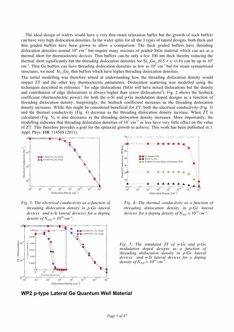
can have very high dislocation densities. In the wafer splits for all the 3 types of lateral designs, both thick and thin graded buffers have been grown to allow a comparison. The thick graded buffers have threading dislocation densities around 106 cm–2 but require many microns of graded SiGe material which can act as a thermal short for thermoelectric devices. Thin buffers can be only a few 100 nm thick thereby reducing the thermal short significantly but the threading dislocation densities for Si1-yGey (0.5 < y <1.0) can be up to 109 cm–2. Thin Ge buffers can have threading dislocation densities as low as 107 cm–2 but for strain symmetrised structures, we need Si1-yGey thin buffers which have higher threading dislocation densities. The initial modelling was therefore aimed at understanding how the threading dislocation density would impact ZT and the other key thermoelectric parameters. Dislocation scattering was modelled using the techniques described in reference 3 for edge dislocations (SiGe will have mixed dislocations but the density and contribution of edge dislocations is always higher than screw dislocations4). Fig. 2 shows the Seebeck coefficient (thermoelectric power) for both the n-Si and p-Ge modulation doped designs as a function of threading dislocation density. Surprisingly, the Seebeck coefficient increases as the threading dislocation density increases. While this might be considered beneficial for ZT, both the electrical conductivity (Fig. 3) and the thermal conductivity (Fig. 4) decrease as the threading dislocation density increase. When ZT is calculated (Fig. 5), it also decreases as the threading dislocation density increases. More importantly, the modelling indicates that threading dislocation densities of 107 cm–2 or less have very little effect on the value of ZT. This therefore provides a goal for the epitaxial growth to achieve. This work has been published in J. Appl. Phys. 110, 114508 (2011).
Fig. 3: The electrical conductivity as a function of
threading dislocation density in p-Ge lateral devices and n-Si lateral devices) for a doping density of NA/D = 1018 cm–3.
Fig. 4: The thermal conductivity as a function of threading dislocation density in p-Ge lateral devices for a doping density of NA/D = 1018 cm–3.
WP2 p-type Lateral Ge Quantum Well Material
22
FIG. 4:
100 102 104 106 108 1010 1012 1014
Dislocation Density [cm-2]
100
102
104
106
Elec
trica
l Con
ducti
vity [
Sm-1 ]
n-channel Si1-xGex designp-channel Si1-xGex design
23
FIG. 5a:
100 102 104 106 108 1010 1012 1014
Dislocation Density [cm-2]
0
10
20
30
40
50
60
70
Therm
al Co
nduc
tivity
[W/K
m]
Ge Quantum WellBarrier Si0.3Ge0.7Weighted Average (Barrier and Quantum Well)
Fig. 5: The simulated ZT of n-Ge and p-Ge modulation doped designs as a function of threading dislocation density in p-Ge lateral devices and n-Si lateral devices for a doping density of NA/D = 1018 cm–3.
20
FIG. 2:
100 102 104 106 108 1010 1012 1014
Dislocation Density [cm-2]10-6
10-4
10-2
100
ZT - D
imen
sionle
ss
n-channel Si1-xGex designp-channel Si1-xGex design
100 104 108 1012
Dislocation Density [cm-2]
0
0.0005
0.001
0.0015
0.002
0.0025
0.003
Z - Fi
gure
of M
erit [K
-1 ]

Page 6 of 47
The samples for this work were grown on 100mm diameter silicon-on-insulator (SOI) substrates consisting of a top Si layer of 340 nm and a SiO2 layer of 1 µm thickness purchased from SOITEC. A thin Si top layer was chosen to minimize parasitic thermal conducting layers for device measurements. The SiGe heterolayers were grown by low energy plasma-enhanced chemical vapor deposition (LEPECVD) at POLIMI. For the design 1 wafer, a single step buffer of nominally 1 µm Si0.2Ge0.8 was grown at a rate of 6 nms–1. For design 2, a two-step (500 nm Si0.6Ge0.4 at 2 nms–1, 500 nm Si0.25Ge0.75 at 6 nms–1) strain relaxed buffer was grown at 475 ˚C in order to form a virtual substrate for the QWs. While this thin buffer features a higher threading dislocation density (TDD) than that which can be obtained with thick graded buffers, a thick buffer would present a significant parallel thermal conduction channel. The superlattices themselves were grown at a rate of around 1.4 nm s–1, a growth rate chosen to allow control of layer content and thickness while ensuring that the whole thermoelectric stack can be realized in a reasonable time. Design 1 consisted of 378 repeats of a 9 nm i-Ge QW, 5 nm i-Si0.3Ge0.7 spacer, 7.5 nm p- Si0.3Ge0.7 supply layer (NA = 1 x 1019 cm–3), and a 5 nm i- Si0.3Ge0.7 spacer all grown on a Si0.2Ge0.8 relaxed buffer layer. The surface of the superlattice was capped with a 5 nm i- Si0.3Ge0.7 spacer, a 7.5 nm p- Si0.3Ge0.7 supply layer (NA = 1 x 1019 cm–3), a 5 nm i- Si0.3Ge0.7 spacer, a 30 nm i-Si0.2Ge0.8 spacer, and a 4 nm i-Si cap. Design 2 consisted of 378 repeats of a 9 nm i-Ge QW, 5 nm i- Si0.4Ge0.6 spacer, 7.66 nm p-Si0.4Ge0.6 supply layer (NA = 1 x 1019 cm–3), and a 5 nm i- Si0.4Ge0.6 spacer all grown on a Si0.25Ge0.75 relaxed buffer layer. The surface of the superlattice was capped with a 5 nm i- Si0.4Ge0.6 spacer, a 7.5 nm p- Si0.4Ge0.6 supply layer (NA = 1 x 1019 cm–3), a 5 nm i-Si0.4Ge0.6 spacer, a 30 nm i-Si0.25Ge0.75 spacer, and a 4 nm i-Si cap. In both cases a 10 µm thick superlattice was chosen so that the active material was approximately 10 times the thickness of the buffer to reduce the electrical and thermal contributions of the buffer and top Si substrate of the SOI. Fig. 6 demonstrates the reciprocal space maps for high resolution x-ray diffraction (HRXRD) scans of the centre of the design 1 wafer undertaken at JKU. From the peak positions in the reciprocal space maps we find that the superlattice structure is pseudomorphic to the relaxed buffer of Si0.18Ge0.82 and is completely strain symmetrized throughout the structure. The clear superlattice peaks in the HRXRD images demonstrate the high quality of the crystal growth.
Fig. 7: The thicknesses (solid symbols) and Ge content (open symbols) across the Design 1 wafer.
Fig. 6: Reciprocal space maps around the (004) and (224) Si-substrate Bragg peak for the centre of the Design 1 wafer. In addition to the substrate peak, superlattice oscillations are observed. The dashed line in the (004) map corresponds to the position of the radial scan used for dynamical scattering theory simulations. The dashed triangle in the (224) map corresponds to the relaxation triangle, spanned by the Si and theoretical Ge (fully relaxed and pseudomorph) Bragg peaks. It can be seen that the 0th-order superlattice peak (SL0) lies exactly on the relaxed line, confirming strain symmetrization.

Page 7 of 47
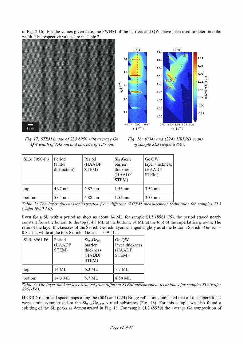
HRXRD characterization was undertaken across all the full wafers by JKU to allow an accurate determination of the heterolayer thicknesses and the Ge content for the barriers and buffer layers. Fig. 7 shows the thicknesses of the QW, barriers and period along with the Ge content of the barriers and buffer layers across the Design 1 wafer. Whilst the HRXRD modelling and results suggest an error in the Ge contents of the barriers of ± < 0.4%, the data measured across the wafer suggests that accuracy may be closer to ±1 %. A similar distribution and uncertainty of thicknesses and Ge contents was also obtained by HRXRD maps for Design 2 (not shown). The SLs were investigated in a Tecnai F30ST TEM operated at 300 kV (0.19 nm point-to-point resolution) at ETH Zurich. The samples were prepared by conventional cross-section preparation (mechanical pre-preparation and Ar-ion etching). TEM was used to provide information about local details not detectable with XRD, such as the origin of surface roughness and short correlation length. The HRXRD quantification of the superlattice period was confirmed by TEM. The layer thicknesses were measured on HRTEM and scanning TEM (STEM) images from the bottom of a QW to the bottom of the next or next-but-one overlaying QW. For the determination of the layer thicknesses, intensity profiles along the growth direction averaged parallel to the interfaces were used. The TEM and HRXRD values of the period thicknesses for the samples are generally in good agreement. Within these studies, it was also found that the bottom heterolayers are undulating (the variation of the periodicity is larger than 1 nm, the exact values depend on the specific area) while the top part of the superlattice stack demonstrates significantly flatter interfaces (Fig. 8(a)). These data are in agreement with the X-ray reflectivity results (which are most sensitive to the top part of the structure). Regarding the material quality, TEM measurements indicated the presence of a rather high TDD, as expected for thin SiGe relaxed buffers. Counting the number of threads on TEM images from a range of samples, TDD densities between 1 and 5 x 109 cm–2 were determined. The dislocations form in the buffer layer and continue to thread into the superlattice layers (Fig. 8 (b, c)). These dislocations give rise to a change of the local heterolayer thicknesses (Fig. 8 (d)). The QWs appear to be thinner close to a threading dislocation. This is partly compensated by a larger thickness of the barriers, which tend to flatten the superlattice surface again. Typically, the thickness change is of the order of 3 to 4 nm over an in-plane length of 30 nm. Similarly to the situation in Si-rich superlattices, the Ge QWs typically provide a rougher surface while Si-rich barriers tend to smoothen the surface again.
Fig. 8: The layer thickness characterization in the top part of the design 1 superlattice demonstrates a high interface quality and a low roughness on a scale of 50 nm. The faint blue frame in the image indicates where the extracted intensity profile, shown in the inset, was taken. b, c A high TDD can be recognized in bright field TEM images in the (220) Bragg condition using only the undiffracted beam for imaging. Dislocations are not restricted to the bottom part of the layers but reach the surface with high density. d High angle annular dark field scanning transmission electron microscopy image in (110) zone axis orientation shows that in the vicinity of dislocations the QWs (bright contrast) are clearly thinner. This is partly compensated by a corresponding increase in thickness of the next barrier layer.

Page 8 of 47
The project started by using the 3ω technique for measuring thermal conductivity but quickly realised that this did not provide accurate results for superlattice material. Therefore a new test structure was developed which allowed the electrical conductivity, thermal conductivity and Seebeck coefficient to be obtained on a single device. To obtain high accuracy of the electrical measurements a Hall bar geometry sample is preferable as provided the correct geometry and length scales are chosen, errors in the measurement of less than 1 part in 104 can be achieved. The Hall bar devices were patterned using i-line photolithography and etched using an inductively coupled plasma reactive ion etch (ICP-RIE) process using a mixture of SF6 and C4F8 to obtain a sloping sidewall profile5. This profile allows metal to run continuously down the sides of the mesa. The SOI buried oxide was used as an etch stop. The Al Ohmic contacts were formed after the sputtering of 300 nm of Al followed by an anneal at 400 ˚C which results in low resistivity electrical contacts to the Ge QWs6. The top of the Hall bar was then coated with 50 nm of inductively-coupled plasma-enhanced chemical vapour deposition Si3N4 to provide an electrically insulating layer to prevent the heaters and thermometers being electrically shorted. Next the heaters were evaporated using 75 nm of NiCr and patterned by lift-off. Then the thermometers were evaporated using a 20 nm Ti, 100 nm Pt bilayer film. 300 nm thick Al interconnects were sputter deposited and patterned by lift-off to provide interconnects to all the electrical connections required to the Hall bar, heaters and thermometers. Photolithography was then used to define rectangles on the oxide beside the Hall bar before RIE was used to first etch through the oxide before a SF6 and N2 isotropic dry etch was used to remove the silicon substrate underneath the Hall bar. Fig. 9 provides a scanning electron microscope (SEM) image of the device and Fig. 10 shows an optical microscope image of the finished devices. A key issue for the design and placement of the heaters and thermometers on the Hall bar is that the heaters provide a uniform temperature across the full cross section of the Hall bar (i.e. the top and bottom of the superlattice stack are at the same temperature) and whilst the thermometers are measuring the surface temperature, this is the same as the bottom of the superlattice. Finite element analysis using Comsol was used to solve Fourier's law to allow the heat transport in the Hall bar device to be modelled for a range of powers being applied to the heaters and for a range of thermal conductivities of the superlattice material. The superlattice was modelled as a uniform layer with 3 different thermal conductivities of 2, 10 and 40 Wm–1K–1 and in all cases, the temperature at the top and bottom of the superlattice stack was identical to within our thermometer measurement accuracy all the way from the hot side thermometer to the cold side thermometer along the Hall bar. The devices were measured in atmospheric pressure as simulations indicated that convection currents should provide an error of 1% or less in the measurement of the temperature along the Hall bar. The electrical conductivity as a function of quantum well width is plotted in Fig. 11. For bulk Ge doped at a comparable level the electrical conductivity is 33,300 S/m and so the modulation doping technique has clearly produced higher values. As the quantum well width is reduced, there is a sudden transition to a reduced electrical conductivity for the design 1 samples which can be attributed to an increase in interface roughness scattering. This is only observed for the samples with a larger amount of Si in the barriers which is why
Fig. 9: A SEM image of a free standing Hall bar device with heaters, electrical contacts and thermometers.
Fig. 10: An optical microscope image of the free standing Hall bar shown in Fig. 9.

Page 9 of 47
interface roughness is the suggested mechanisms. This spacer layer (the undoped spacer between the doping supply layer and the quantum well) is not a constant and will also decrease for the narrower quantum well. The position of the dopant has not been measured in these samples and so the thickness of the spacer layer between the quantum well and the doping supply layer is unknown. Whilst the uncertainty in the measurement of electrical conductivity is below 1% of the measured values, the variation observed between the samples is much larger than this value. It is believed that local variations in the high threading dislocation density for each sample results in the variability as the electrical conductivity is very sensitive to the dislocation density in this regime.
The Seebeck coefficient was taken as the gradient of the Seebeck voltage versus the temperature difference measured down the length of the Hall bar as a heater at one end created the temperature difference. Fig. 12 demonstrates the variation of the Seebeck coefficient measured as a function of the quantum well width. For this set of samples, the results suggest that the Seebeck coefficient is near constant and it is believed that the small variability in the results is related to local changes in the threading dislocation across the samples being characterized. These results with values between 236.0 ± 3.5 and 279.5 ± 1.2 µV/K should be compared with a bulk p-type Ge Seebeck coefficient of 90 µV/K at 300 K with comparable doping density of ~1019 cm–3 and thin film p-Ge samples of 300 µV/K. As a high dislocation density can also increase the Seebeck coefficient, the present results do not yet demonstrate beyond all reasonable doubt that the enhanced Seebeck coefficient is the result of a larger asymmetry across the chemical potential as suggested by the Cutler & Mott equation7. Further samples with lower dislocation density are required before the true mechanism for the enhanced Seebeck coefficient can be determined. The power factor as a function of quantum well width has been plotted in Fig. 13. The values need to be compared with bulk p-Ge of 2.45 x 10⁻⁴ Wm–1K–2 and for thin film p-Ge of 1.33 x 10⁻³ Wm–1K–2. All the values demonstrate enhancements with the best samples producing power factors six times larger than bulk thin film Ge for a comparable doping density8. To obtain the thermal conductivity, a measurement of the heat flux being injected into the hot end of the Hall bar is required. To obtain this, the temperature at each end of the Hall bar was measured using the calibrated thermometers. The Hall bar was then removed allowing the heat that is being transported through parasitic channels such as the electrical, heater and thermometer contacts to the Hall bar to be measured. By evaluating how much additional power is required with the Hall bar central section in place to get the hot end of the device to the same temperature, an accurate heat flux being injected into the Hall bar can be extracted. Fourier's law can then be used to calculated the thermal conductivity since the temperature gradient along the Hall bar is known as well as the heat flux entering the Hall bar at the hot end and the length of the measurement section. Fig. 14 presents the thermal conductivity results from the samples as a function of quantum well width. There is a general trend of lower thermal conductivities for narrower quantum wells for the design 1 samples as would be expected since the diffuse phonon scattering should increase as the quantum well width is reduced. For the design 2 samples with the larger Si content in the barriers, more interface
Fig. 11: The electrical conductivity of the samples as a function of quantum well width at 300 K. Design 1 (blue squares), design 2 (red circles).
Fig. 12: The Seebeck coefficient as a function of quantum well width at 300 K. Design 1 (blue squares), design 2 (red circles).
Fig. 13: The Power factor as a function of quantum well width at 300 K. Design 1 (blue squares), design 2 (red circles).

Page 10 of 47
roughness scattering is expected and this will make the phonon scattering less diffuse and more specular resulting in higher thermal conductivity9,10.
The ZT for the samples as a function of quantum well width is presented in Fig. 15. For bulk Ge, the ZT is 1.15 x 10⁻³ ref. 11 whilst for thin film Ge it is 6.23 x 10⁻³. The present results represent an order of magnitude increase in the ZT figure of merit over bulk Ge demonstrating the benefits of low dimensional structures for improving the ZT. The values, however, are also higher than the best reported Si0.3Ge0.7 results at the same carrier density12 although the present modulation doped samples also have a power factor which is six times larger than the bulk values. The ZT values are still rather low compared to the best bulk material at 300 K Bi2Te3. Initial analysis suggests that all the present samples have significant electrical conductivity in the Si1-xGex barriers and therefore optimising the spacer and doping supply layers should allow improved results especially through enhancements to the Seebeck coefficient through the reduced doping. A second issue is that the ZT is strongly dependent on the threading dislocation density for densities above 107 cm–2 as shown in the modelling section above. The modelling at UGLA suggests that a reduction of the threading dislocation density to 107 cm–2 or below would increase the ZT by an order of magnitude13 which would result in ZT values comparable to the best Bi2Te3 results at room temperature. The power factors are already above bulk Bi2Te3 at room temperature and these values are expected to improve by a reduction of the threading dislocation density. p-type Vertical Superlattice Thermoelectric Designs A range of p-type Ge/Si0.5Ge0.5 superlattices with different QW, barrier thicknesses and doping were designed and grown to investigate the cross-plane thermoelectric properties i.e. with the electrical and thermal transport perpendicular to the QWs and barriers. Cross-plane designs should have higher Seebeck coefficients from the higher density of states asymmetry in the thinner QWs14,15 and lower thermal conductivity due to increased heterolayer phonon scattering16,17 over the in-plane designs. The samples were grown on 100 mm diameter p-Si (001) substrates of 5-10 Ω-cm using low-energy plasma enhanced chemical vapor deposition (LE-PECVD) by Polimi. A ~13 µm graded buffer layer from Si to Si0.175Ge0.825 was grown at a rate of between 5 and 10 nms–1. This graded buffer has a threading dislocation density ~106 cm–2 which is substantially below the densities for thin buffers. Then a 500 nm bottom contact of p-Si0.175Ge0.825 (NA = 2.0 x 1018 cm–3) layer was grown. The superlattices were grown at a rates of 1.0 to 1.5 nm.s–1 for designs SL1 (wafer 9097) and SL2 (wafer 9151) and 0.25 nm.s–1 for SL3 (wafer 8950), SL4 (wafer 8957) and SL5 (wafer 8961). These growth rates were chosen to allow control of the layer content and thickness while ensuring that the whole thermoelectric stack could be realized in a reasonable time. First 10
Fig. 14: The thermal conductivity as a function of quantum well width at 300 K. Design 1 (blue squares), design 2 (red circles), design 2 ThAFM (green triangle).
Fig. 15: The ZT as a function of quantum well width at 300 K. Design 1 (blue squares), design 2 (red circles).

Page 11 of 47
nm of graded p-Si1-xGex with x from 0.8 to 1.0 and a 5 nm p-Ge heterolayer were grown before the superlattices. Two experiments have been undertaken. The first was aimed at investigating the effect of doping density. Designs SL1 to SL4 consisted of 922 repeats of QWs of 2.85 ± 1.5 nm p-Ge and 1.1 ± 0.6 nm of p-Si0.5Ge0.5 with the doping density increasing from NA = 1.9 x 1017 cm–3 to 2.0 x 1018 cm–3. The second experiment was to investigate the effect of smaller QWs and barriers on samples with larger miniband width. Design SL5 consisted of 2338 repeats of QWs of 1.1 nm p-Ge and 0.6 nm of p-Si0.5Ge0.5. For design SL4, only the barriers were doped at NA = 6.0 x 1018 cm–3 to produce an average doping of NA = 1.2 x 1018 cm–3. Finally a cap of 60 nm of p-Ge (NA = 2.0 x 1018 cm–3) was grown for a top Ohmic contact. A summary of the designs is shown in table 2.
The band structure for SL2 with the 2.57 nm Ge QW was calculated using a self-consistent 8-band k.p Poisson-Schrödinger solver with the deformation potentials in ref.18. The valence bands and the three lowest uncoupled subband states are shown in Fig. 16 left. The barriers are thin enough that minibands are formed from the coupling of the subband states in each QW. The miniband widths for SL1 to SL4 are between 8 meV and 26.3 meV. SL5 with the narrower QWs has a miniband width of 263 meV. For all the results presented, increasing the doping has a significantly larger effect on the electrical conductivity than increasing the miniband width. The thin QW (a = 1.18 nm and b = 0.51 nm) and barriers of SL5 also produces phonon bandgaps of around 5 meV in the acoustic phonon spectra as calculated using a 1D Rytov model19 (see Fig. 16 right). The heterolayer thicknesses were determined by HRXRD at JKU and scanning transmission electron microscopy (STEM) at ETH. Fig. 17 demonstrates a STEM image of SL3. For a SL with a period of about 36 monolayers (ML) the variations are in the range of 35.7 ± 0.4 ML which is within the measuring error (the average over 5 – 10 periods was used in order to reduce the influence of local variations of the layer thicknesses). From diffraction a value of 5.04 nm at the bottom and one of 4.97 nm at the top have been determined for the period of this superlattice. The deviation is within the measuring error of about 2% and demonstrates excellent uniformity of the period thickness through the ≥4 µm superlattice growth. The determination of the thicknesses of the individual layers was not totally unambiguous, because on one side they are not totally flat, which leads to an averaging in the projection view of a TEM image. Additionally, the top interface of the Si-rich layers is more abrupt than the one of the Ge-rich layers (see intensity line scans
Fig. 16: Left: The valence band edges and the superlattice dispersion as calculated by 8-band k.p theory for sample SL2 (9151). Right: The acoustic phonon superlattice dispersion for samples SL5 (8961) demonstrating phonon bandgaps. a is the QW width, b is the barrier width and kz is the superlattice phonon wavevector in the quantised direction.
Page 12 of 47
in Fig. 2.16). For the values given here, the FWHM of the barriers and QWs have been used to determine the width. The respective values are in Table 2.
SL3: 8950-F6 Period (TEM diffraction)
Period (HAADF STEM)
Si0.5Ge0.5 barrier thickness (HAADF STEM)
Ge QW layer thickness (HAADF STEM)
top 4.97 nm 4.87 nm 1.55 nm 3.32 nm
bottom 5.04 nm 4.88 nm 1.55 nm 3.33 nm Table 2: The layer thicknesses extracted from different (S)TEM measurement techniques for samples SL3 (wafer 8950-F6). Even for a SL with a period as short as about 14 ML for sample SL5 (8961 F5), the period stayed nearly constant from the bottom to the top (14.3 ML at the bottom, 14 ML at the top) of the superlattice growth. The ratio of the layer thicknesses of the Si-rich:Ge-rich layers changed slightly as at the bottom: Si-rich : Ge-rich = 0.8 : 1.2, while at the top: Si-rich : Ge-rich = 0.9 : 1.1.
SL5: 8961 F6 Period (HAADF STEM)
Si0.5Ge0.5 barrier thickness (HADDF STEM)
Ge QW layer thickness (HAADF STEM)
top 14 ML 6.3 ML 7.7 ML
bottom 14.3 ML 5.7 ML 8.58 ML Table 3: The layer thicknesses extracted from different STEM measurement techniques for samples SL5(wafer 8961-F6). HRXRD reciprocal space maps along the (004) and (224) Bragg reflections indicated that all the superlattices were strain symmetrized to the Si0.175Ge0.825 virtual substrates (Fig. 18). For this sample we also found a splitting of the SL peaks as demonstrated in Fig. 18. For sample SL3 (8950) the average Ge composition of
Fig. 18: (004) and (224) HRXRD scans of sample SL3 (wafer 8950).
Fig. 17: STEM image of SL3 8950 with average Ge QW width of 3.43 nm and barriers of 1.17 nm.

Page 13 of 47
the red enclosed peaks was found to be 86 % whereas for the green enclosed peaks an average composition of 85.7 % was found. Interestingly the period seemed to stay constant. From the conventional laboratory measurements with a large X-ray beam of a few mm diameter, it was not clear whether this abrupt change in composition happened laterally or vertically along growth direction. For this reason reciprocal space maps with a 1x1 mm beam were obtained on one sample piece at 9 different positions with a rotating anode setup. The obtained reciprocal space maps showed the same picture (within the known gradual period change due to the lateral growth inhomogeneities) for the 9 different positions. Thus it could be concluded, that at some point during the growth a composition change must have occurred, which resulted in this splitting. Unfortunately this could not be seen in the TEM analysis due to the limited field of view. A variation in the Ge content of 0.3% for the barriers over the complete 4 µm stack will have negligible effect on the thermoelectric properties under study. Indeed, a variation of 0.3% in Ge content combined with the STEM measurements of the layer thicknesses indicates that the LEPECVD has excellent reproducibility throughout the superlattice.
The cross-plane electrical conductivity was measured by fabricating a range of different circular transfer line method (CTLM) devices each with different gap spacings between the two terminal Ohmic contacts. Ni was deposited by an electron-beam evaporator and annealed at 340 ˚C to form NiGe Ohmic contacts6. These devices were measured as a function of gap spacing to extract the contact resistances due to the metal-semiconductor junction. After this initial measurement, the devices were modified by etching anisotropically the film between the contacts by a fluorine based low-damage reaction ion etch5 developed in the project. They were measured again as a function of the gap spacing for eight different etch depths from 0 µm to the maximum thickness of the thin film, 3.5 µm. For each of these eight etches the intercept resistance, when the gap spacing was 0 µm, was extracted and plotted as a function of etch depth, see Fig. 19 and 20. The two terminal resistance which is measured will extract two contact resistances (2Rc) for the Ohmic metal to the superlattice, twice the suerlattice resistance (2RSL) and a contribution from the lateral resistance (RLateral) which should be negligible due to the 500 nm thick p-SiGe buried contact and the electrical conductivity of the thick substrate. The gradient of these data points allowed the electrical conductivity perpendicular to the superlattice to be calculated (Fig. 20). The measured values of the electrical conductivity are presented in Table 4 and are smaller than bulk p-Ge and p-SiGe results. This is to be expected with the additional interface roughness scattering at the Ge/Si0.5Ge0.5 heterointerfaces.
Fig. 19: A schematic diagram showing a cross section of the CLTM structures with variable etch depth used to extract the vertical electrical conductivity of the superlattices.
Fig. 20: The two terminal electrical conductivity from CTLM structures as a function of etch depth for SL1: Insert: an optical microscope image of the CTLM device and a schematic diagram of the measurement.
Page 14 of 47
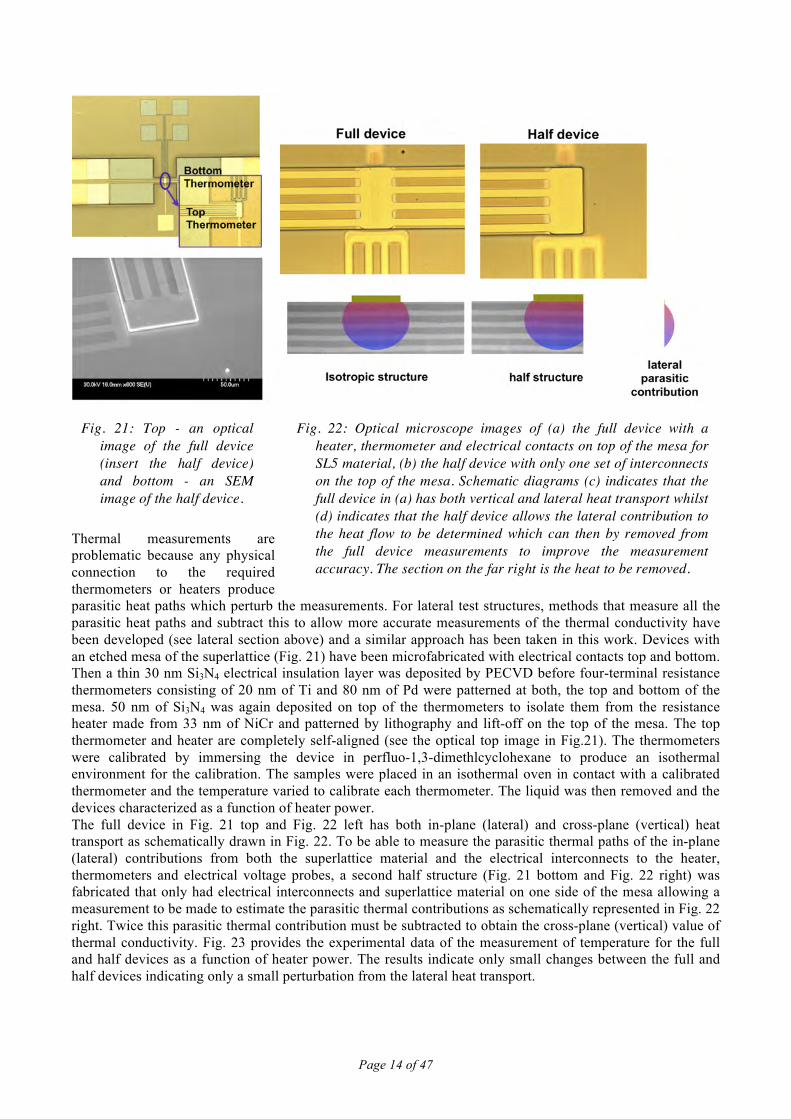
Thermal measurements are problematic because any physical connection to the required thermometers or heaters produce parasitic heat paths which perturb the measurements. For lateral test structures, methods that measure all the parasitic heat paths and subtract this to allow more accurate measurements of the thermal conductivity have been developed (see lateral section above) and a similar approach has been taken in this work. Devices with an etched mesa of the superlattice (Fig. 21) have been microfabricated with electrical contacts top and bottom. Then a thin 30 nm Si3N4 electrical insulation layer was deposited by PECVD before four-terminal resistance thermometers consisting of 20 nm of Ti and 80 nm of Pd were patterned at both, the top and bottom of the mesa. 50 nm of Si3N4 was again deposited on top of the thermometers to isolate them from the resistance heater made from 33 nm of NiCr and patterned by lithography and lift-off on the top of the mesa. The top thermometer and heater are completely self-aligned (see the optical top image in Fig.21). The thermometers were calibrated by immersing the device in perfluo-1,3-dimethlcyclohexane to produce an isothermal environment for the calibration. The samples were placed in an isothermal oven in contact with a calibrated thermometer and the temperature varied to calibrate each thermometer. The liquid was then removed and the devices characterized as a function of heater power. The full device in Fig. 21 top and Fig. 22 left has both in-plane (lateral) and cross-plane (vertical) heat transport as schematically drawn in Fig. 22. To be able to measure the parasitic thermal paths of the in-plane (lateral) contributions from both the superlattice material and the electrical interconnects to the heater, thermometers and electrical voltage probes, a second half structure (Fig. 21 bottom and Fig. 22 right) was fabricated that only had electrical interconnects and superlattice material on one side of the mesa allowing a measurement to be made to estimate the parasitic thermal contributions as schematically represented in Fig. 22 right. Twice this parasitic thermal contribution must be subtracted to obtain the cross-plane (vertical) value of thermal conductivity. Fig. 23 provides the experimental data of the measurement of temperature for the full and half devices as a function of heater power. The results indicate only small changes between the full and half devices indicating only a small perturbation from the lateral heat transport.
Fig. 21: Top - an optical image of the full device (insert the half device) and bottom - an SEM image of the half device.
Fig. 22: Optical microscope images of (a) the full device with a heater, thermometer and electrical contacts on top of the mesa for SL5 material, (b) the half device with only one set of interconnects on the top of the mesa. Schematic diagrams (c) indicates that the full device in (a) has both vertical and lateral heat transport whilst (d) indicates that the half device allows the lateral contribution to the heat flow to be determined which can then by removed from the full device measurements to improve the measurement accuracy. The section on the far right is the heat to be removed.

Page 15 of 47
The measured values of Seebeck coefficients and thermal conductivities with standard deviations are presented in Table 2.4. The expected uncertainties in the thermal conductivity measurement is about 10 % whilst the standard deviations are well below this figure. Measurement of reference samples of SiO2 produced a thermal conductivity of 1.7 ± 0.6 Wm–1K–1 which compares well with literature values of 1.6 Wm–1K–1 20 and provides some confidence in the approach. For samples SL5 with QW of 1.18 nm and barriers 0.5 nm in thickness, the measured Seebeck coefficients were 91.8 µV/K and comparable to bulk SiGe12 and SiGe quantum dot21 values suggesting the holes see the material as a random bulk alloy rather than a superlattice. The thermal conductivities are between 5.1 and 5.6 Wm–1K–1 which are lower than comparably doped bulk Si0.3Ge0.7 but higher than undoped Si/Ge superlattices on Si (111) and Si (100) substrates22. The low electrical conductivity results in the electronic contribution to thermal conductivity being only a few percent. This is also clearly demonstrated by measurement on the undoped superlattice 8997 which has comparable thermal conductivity to the doped samples (see Table 4). The measured figure of merit ZT was 0.080 which is ~60 % the values for lateral p-type Ge/SiGe superlattices and SiGe quantum dots but four times higher than bulk SiGe alloys with comparable Ge content. The highest ZT occurred for uniform doping with one of the widest QWs and the power factor is comparable to the best p-SiGe ZT material. The major difference is that the thermal conductivity is twice the value of the SiGe QD results. Chen23 demonstrated that on Si/Ge superlattices a high specular scattering coefficient was required to understand the thermal conductivity values using an inelastic acoustic mismatch model implying that interface roughness scattering had a strong influence on the thermal conductivity. Such models for the present Si0.5Ge0.5 barriers and superlattice periodicity suggest a minimum of the thermal conductivity value of ~1 Wm–1K–1 indicating that interface roughness scattering is still a significant influence in the present vertical p-type samples. Interface roughness in SiGe materials is known to increase as a function of strain (and therefore Ge content difference) suggesting a reduction in the strain difference (Ge content difference) between the QWs and barriers should reduce the thermal conductivity and increase the electrical conductivity resulting in higher power factors and ZTs. Sample NA (cm–3) QW
/barrierwidth (nm)
σ (S m–1) κ (W m–
1K–1) α (µV K–
1) ZT (300 K) α2σ
(mWK–2m–
1) SL1: 9097 1.9x10¹⁷ 3.03 / 0.97 2220±62 6.0 ± 0.4 533 ± 25 0.031±0.003 0.63±0.06 SL2: 9151 9.7x10¹⁷ 2.57 / 0.82 6680±8630 4.5 ± 0.4 393 ± 7 0.068±0.010 1.03±0.06 SL3: 8950 2.0x10¹⁸ 3.43 / 1.17 8630±910 5.1 ± 0.4 394 ± 6 0.080±0.011 1.34±0.15 SL4: 8957 δ:
1.2x10¹⁸ 2.48 / 1.12 17600±3330 5.6 ± 0.3 113 ± 7 0.012±0.003 0.22±0.05
SL5: 8961 2.0x10¹⁸ 1.18 / 0.51 15500±1490 5.1 ± 0.1 91.8 ± 2.8
0.0077±0.0001 0.13±0.015
8997 undoped 2.6 / 0.9 5.28 ± 0.4
Table 4: A summary of the main results from the different samples along with a comparison with a range of bulk materials at 300 K. The QW widths were extracted by HRXRD measurements of each sample.
Fig. 23: The thermometers on the top (TH) and on the bottom (Tc) of the full and half devices for SL1 - 9097.

Page 16 of 47
n-type Vertical Superlattice Thermoelectric Designs Two different designs were undertaken for the n-type vertical thermoelectric material. Our designs have
concentrated on barriers with nm dimensions with the aim to scatter the acoustic phonons that contribute the most to the thermal conduction. The first set of samples investigates whether thick or thin QWs have any significant impact on the ZT. The expectation is that the wider QWs will have a lower Seebeck but a higher electrical conductivity and a comparable thermal conductivity. Designs 1 and 4 (see Table 5) have narrow and wide quantum wells respectively to investgate which will give the higher ZT. Fig. 24 provides the conduction band edges for the L- and Δ-valleys and the L-miniband dispersion for Design 1. The miniband width is 45.4 meV as calculated by self-consistent Poisson-Schrödinger equation using the deformation potentials in ref.18. The Δ2 valleys in the L-valley barrier have the lowest subband energies in the structure but these states are not coupled to form minibands since the effective mass for the Δ2-valley electrons is m* = 1.22m0 in the barrier and m* = 1.35m0 in the Ge QW. The states are confined and not extended and therefore do not contribute to the conduction except through scattering other carriers. For the L-valley electrons, the effective masses are m* = 0.118m0 in the Ge QW and m* = 0.139m0 in the barrier so the subbands are coupled forming extended states of minibands as shown in Fig. 24. For design 4, the miniband width is calculated to be 2.45 meV i.e. substantially smaller than Design 1. Therefore if miniband transport dominates the vertical electrical transport, from the Tsu-Esaki model where mobility is proportional to the width of the miniband, one would expect Design 1 to have higher electrical transport. The superlattice acoustic phonon dispersion was also calculated using the 1D model of Rytov19. For these QW and barrier widths, whilst phonon bandgaps are produced, the gaps are only ~1 meV in energy and therefore are unlikely to have any major effect on the thermal transport.
Fig. 24: Left: The superlattice dispersion of the lowest 2 L-valley minibands and the band edges for the L-
and Δ-valleys for Design 1, sample 8719. Right: the superlattice acoustic phonon dispersion calculated by the Rytov 1D model19.
The second design aims to scatter more acoustic phonon wavelengths by increasing the number of barriers
and different barrier widths in the important 1.2 to 3.5 nm range of acoustic phonon wavelengths for transport. The designs were grown by LEPECVD at Polimi with TEM characterisation at ETH Zurich and HR-XRD
at JKU. For these structures, thick graded buffer layers were used to minimise the number of threading dislocations. TEM images indicates that the TDD is below 108 cm–2 while further analysis on previous samples with the same buffer suggests the TDD is around 106 cm–2. Figs. 25 show the top of the superlattice stack for the Design 1, wafer 8719. Within the accuracy of the TEM technique there is very little difference in the thicknesses measured at the top and bottom of the superlattice stack. There is a level of interface roughness similar to the p-type layers of around a few monolayers.
Fig. 26 shows the top TEM images of Design 6, wafer 8722 with the heterolayer thicknesses marked. The layers appear to be better defined and narrower at the top of the superlattice close to the surface compared to the bottom at the start of the superlattice growth although the period for the top was measured as 43.40 nm

Page 17 of 47
whilst the bottom is 43.45 nm. Analysis of the TEM images of the Si0.3Ge0.7 barriers indicate that they are definitely reducing in thickness from the left to the right of each period in the images. Higher resolution images (not shown) indicate that there are local lateral variations in the barrier thicknesses (2.5 / 1.78 / 1.3 nm compared to 3.4 / 2.8 / 1.2 nm). The bottom of the layer stack in HRTEM are much more fuzzy making accurate measurements more difficult. This is probably due to beam damage during the characterisation but may also be related to a large point defect density in the material.
Figs. 27 demonstrate the (004) and (224) Bragg reflections for samples 8717 Design 4. The superlattices are homogeneously strained to the relaxed substrate. A number of artifacts are present in the images.
The electrical conductivity was measured for these n-type vertical samples using the sample CTLM structures with different etch depths as previously described for the p-type vertical samples (Figs. 19 and 20). Fig. 28 shows the electrical conductivity as a function of temperature for sample 8719 Design 1. The error bars in Fig. 2.40 were calculated from the least squares linear correlation coefficient (Pearson’s R) from the linear fit to the data. The results for Designs 4, 5 and 6 at 300 K are reported in Table 5.
Fig. 25: A STEM image of the top of the superlattice for sample 8719.
Fig. 26: HAADF-STEM image of the top of 8722 G9 Design 6: 14.9 / 2.5 / 14.3 / 1.78 / 13.9 / 1.3 nm for Ge QW and Si0.3Ge0.7 barriers.
Fig. 27: (004) and (224) HRXRD scans of sample 8722 Design 6.
Fig. 28: The electrical conductivity of sample 8719 Design 1 as a function of temperature.

Page 18 of 47
For the thermal measurements, vertical test structures with thermometers, heaters and electrical contacts were microfabricated identical to those used for the vertical p-type measurements and described in Figs. 21 and 22. The probe station used for measurements limited the maximum temperature of measurement to below 120 ˚C. The Seebeck voltage as a function of ΔT was measured between the top and bottom of the superlattice for 2 different devices fabricated using wafer 8722, Design 6 which produced a Seebeck coefficient of –405 µV/K. The doping density in the present samples was 2x1018 cm–3 which is lower than most of the bulk SiGe thermoelectric material. Therefore higher Seebeck coefficients than bulk material are expected since the Seebeck coefficient is proportional to N–2/3 for bulk materials. The increase of the Seebeck coefficient from –320 µV/K to –455 µV/K from Design 4 to Design 1 is for identical doping and the only change is the reduction in the QW from 12.2 to 4.64 nm. This is clear evidence of 2D enhancement to the Seebeck coefficient from quantum confinement. More interesting is the Seebeck enhancement from Design 4 to Design 6. Here there is enhancement but in wide QWs suggesting the miniband structure is enhancing the Seebeck coefficient rather than the QW width. The lower Seebeck coefficient from Design 5 indicates that the effect is not a simple effect and further analysis is required to fully understand how to maximise the Seebeck coefficient. The temperature dependence for samples 8719 Design 1 is shown in Fig. 29 and demonstrates a linear increase as the temperature is increased. This is to be expected in all derivations of the Seebeck coefficient. The measured gradient in Fig. 29 is 3 times larger than the expected value for bulk material given by suggesting confinement effects are involved. Here kB is Boltzmann’s constant, q is the eletron charge, h is Planck’s constant, m* is the effective mass, T is the temperature and N is the doping concentration in the material.
The thermal conductivity was measured using the full and half devices as described for the p-type vertical material. Fig. 30 shows the hot and cold temperatures for the full and half devices as a function of heat power on top of the device. There is more variability in this measurement than the p-type devices but linear fits to the results indicate on a small variation between the full and half devices. The electrical contribution to the thermal conductivity from the free electron model is κel = π2kBTσ/3q2 which corresponds to 4.7%, 4.8%, 7.5% and 5.8% contributions to the thermal conductivities for Designs 1, 4 5 and 6 respectively. The higher thermal conductivities compared to the p-type material is therefore partly related to the higher electrical conductivity and the electrical contribution. Designs 4, 5 and 6 were aimed at testing if the thermal conductivity reduces as additional barriers with different thicknesses at the key wavelengths to scatter acoustic phonons were added. The results in table 5 demonstrate a clear reduction as the number of barriers is increased. This potentially suggests that higher ZTs could be achieved by adding even more than 3 barriers to future designs.
Table 5 presents the ZT for all the designs at 300 K compared to results from the literature. All the results have higher ZTs than all reported Si, Ge and SiGe results reported in the literature. Fig. 31 presents the temperature dependence of sample 8719 Design 1 compared to the main thermoelectric materials of Bi2Te3, PbTe and bulk SiGe. The present results are the highest reported ZT for a Te-free material. Our industrial steering committee have stated that industry would like to remove tellurium from thermoelectrics as it is the 9th rarest element on earth. This makes tellurium based thermoelectrics unsustainable and at present materials
Fig. 29: The Seebeck coefficient as a function of temperature for wafer 8719 Design 1.
Fig. 30: The thermal conductivity as a function of temperature for wafer 8719 Design 1.

Page 19 of 47
markets have substantial fluctuations in the price of tellurium.
Perhaps more important for applications is that the power factor for Design 1 is 10.4 ± 1.0 mWK–2m–1 which is one of the highest reported values for high ZT materials. It is 2.8 times larger than Bi2Te3 at room temperature. Sample NA (cm–3) QW
/barrierwidth (nm)
σ (S m–1) κ(Wm–1K–
1) α (µV.K–1) ZT (300
K) α2σ (mWK–
2m–1) Design 1 8719
2x10¹⁸ 4.64 / 1.55 50,200 ± 4,200
6.4 ± 0.7 –455 ± 9 0.49 ± 0.04
10.4 ± 1.0
Design 4 8717
2x10¹⁸ 12.2 / 2.3 55,900 ± 7,700
8.6 ± 0.5 –320 ± 4 0.20 ± 0.03
5.7 ± 0.8
Design 5 8802
2x10¹⁸ 9.3 / 1.8 9.3 / 2.6
82,000 ± 12,400
7.4 ± 0.5 –295 ± 33 0.29 ± 0.08
7.1 ± 1.9
Design 6 8722
2x10¹⁸ 16.7 / 2.8 16.0 / 2.0 15.5 / 1.5
53,000 ± 9,200
6.6 ± 0.5 –403 ± 3 0.39 ± 0.08
8.6 ± 1.5
Table 5: A summary of the results from each n-type vertical design. Si and SiGe Nanowires
Si nanowires were developed with integrated electrical contacts, heaters and thermometers to allow all the
main thermoelectric parameters to be measured. Fig. 32 shows a SEM image of the finished array of one hundred 45 nm wide Si nanowires. One hundred nanowires in parallel were chosen to aid the characterisation as the electrical and thermal resistance of a single nanowire is so high.
The nanowires were fabricated by UGLA. For the fabrication of the silicon nanowires, 200 mm diameter Silicon-On-Insulator (SOI) substrates with a Si top layer of 55 nm p-doped to 4 x 1015 cm–3 and with a buried oxide of 150 nm were used. The starting p-type wafers were implanted with P to doping densities ranging between 1x1018 cm–3 and 5x1020 cm–3 followed by activation of the dopant with a two step process with a short 900 °C spike anneal of 3 seconds followed by a long 600 °C anneal of 30 minutes. A dilution of hydrogen silsesquioxane (HSQ) 1:7 methyl isobutyl ketone (MIBK) was spin coated onto the substrates at 5000 rpm resulting in a measured 30 nm thick resist on the SOl substrate. A Vistec VB6 UHR electron-beam lithography tool was used to write the patterns with nanowires of widths from 5 to 100 nm line and a dose of 2700 µC/cm–2 with a 1 nA current at 100 keV accelerating voltage. The devices were subsequently developed using a 25 % tetramethyl ammonium hydroxide (TMAH) based solution diluted further 1:3 with deionized water at a temperature of 23°C for 1 minute followed by 2 separate rinses in deionized water for 30 seconds each and a final IPA rinse for 15 seconds. This process has been optimized to achieve high resolution features with resist line widths below 5 nm.
Fig. 31: The ZT as a function of temperature for wafer 8719 Design 1 and compared to n-Bi2Te3, n-PbTe and n-Si0.7Ge0.3. The red line is a linear fit to the data.

Page 20 of 47
Fig. 32: SEM images of one hundred 45 nm wide free-standing Si nanowires on a 150 nm SiO2 membrane
with heaters, thermometers and electrical contacts to measure ZT. TEM cross sections are present in Fig. 33.
The devices were then etched using a STS inductivity coupled plasma (ICP) reactive ion etch tool using
SF6/C4F8 : 25/90 sccm gas flow ratio, 10 mtorr of chamber pressure and 600/6 (coil/platen) RF power. The etching chemistry and parameters were optimized to deliver highly anisotropic etch in silicon under a bias voltage of –20 V. The nanowires were thermally oxidised at 950 ˚C for 90 seconds in O2 gas to form a 3 nm SiO2 passivation. Electrical contacts were made by etching holes in the SiO2 thermal oxide before depositing 20 nm of Ni followed by 50 nm of Pt and patterning by lift-off. An anneal at 450 ˚C was used to form NiSi electrical Ohmic contacts with specific contact resistivities of ~10–8 Ω-cm2. Next heaters consisting of 75 nm of electron beam evaporated NiCr were patterned, deposited and lifted off. Four terminal thermometers were patterned close to the ends of the nanowires using 20 nm of Ti with 100 nm of Pt. Al interconnects to the thermometer and Ohmic contacts were then patterned before holes were etched in the buried 150 nm SiO2. Finally a SF6 isotropic etch was used to etch away the substrate leaving the whole structure free standing as demonstrated in Fig. 32. TEM cross sections of some of the different width fabricated nanowires are presented in Fig. 33.
All the measurements to be reported are for one hundred 45 nm wide Si nanowires doped to 8x1019 cm–3 which have measured sheet resistivities indicating doping of 4x1019 cm–3. It is believed that during the thermal processing some of the dopant diffused out of the nanowires thus resulting in the lower measured doping density although non-activation of the dopants would be another possible reason for the difference.
Fig. 33: Two TEM images demonstrating the cross sections of Si nanowires before being made free standing.
Fig. 34: The 2 terminal and 4 terminal electrical measurements at 300 K for the Si nanowires doped at 4 x 1019 cm–3.

Page 21 of 47
The Seebeck voltage was measured as a function of ΔT across the nanowires as one of the heaters had a current being applied. The Seebeck voltage as a function of ΔT has a gradient of –271 µV/K for the Seebeck coefficient. This value of Seebeck coefficient is around 3 times higher than the value of –95 µV/K for bulk Si of comparable doping.
To obtain the thermal conductivity, a technique similar to the lateral devices was used. First the hot and cold temperatures along the complete set of nanowires on top of the SiO2 membrane was measured as a function of the heater power before a second measurement was undertaken on a nominally identical sample fabricated without the Si nanowires. This allows the parasitic thermal paths to be measured and subtracted from the complete device thermal measurements leaving the results for only the thermal conductivity of the nanowires. The result is a thermal conductivity of 7.8 W m–1K–1 which is around a 20 times reduction in the thermal conductivity from bulk Si. These numbers are quite comparable to the thermal conductivity for polycrystalline Si materials and SiGe alloys indicating that the phonon scattering lengths in the nanowires must be becoming comparable to those in polycrystalline material and SiGe alloys.
Finally the electrical conductivity was measured as shown in Fig. 34. For the 45 nm nanowires used in this work, the four terminal measurements of a single nanowire produce an electrical conductivity of 20,300 S/m. This is a little higher than bulk Si with a slightly lower doping of 1x1019 cm–3 suggesting that the electrical properties at these length scales are still 3D in electrical behaviour. Further measurements are planned after the project to extract the carrier density and mobility to fully understand the electrical behaviour of these nanowire devices. Putting all the measurements together produces a ZT of 0.057 at 300 K which is an enhancement of 117 over bulk Si of comparable doping density.
Sample Width (nm) σ (S m–1) κ (W m–
1K–1) α (µV K–1) ZT (300 K) α2σ (WK–
2m–1) n-Si lateral nanowire
45 nm width
20,300 7.8 –271 0.057 0.00149
Table 6: The electrical and thermal properties of the Si nanowires. Whilst these enhancements are impressive over bulk Si, the ZT is still quite modest for the nanowires. Also
lateral nanowires would produce very low nanowire densities if integrated into lateral modules. SiGe nanowires and even better from the high ZT results from Ge/SiGe superlattices suggests that superlattice nanowires could potentially have substantially higher ZTs. Therefore work was undertaken to form n-Ge/SiGe superlattice nanowires. Fig. 35 is an SEM image of 50 nm wide n-Ge/Si0.3Ge0.7 nanowires which are 4 µm tall. These have been fabricated with the aim of ultimately being able to use the array to flip chip bond into modules. With more time in the project then thermoelectric measurements of these Ge/SiGe nanowires would have been undertaken but unfortunately there was not sufficient time to complete this work before the final report.
Fig. 35: A SEM image of 50 nm wide and 4 µm tall Ge/SiGe superlattice nanowires etched by low-damage fluorine dry etch.
Page 22 of 47
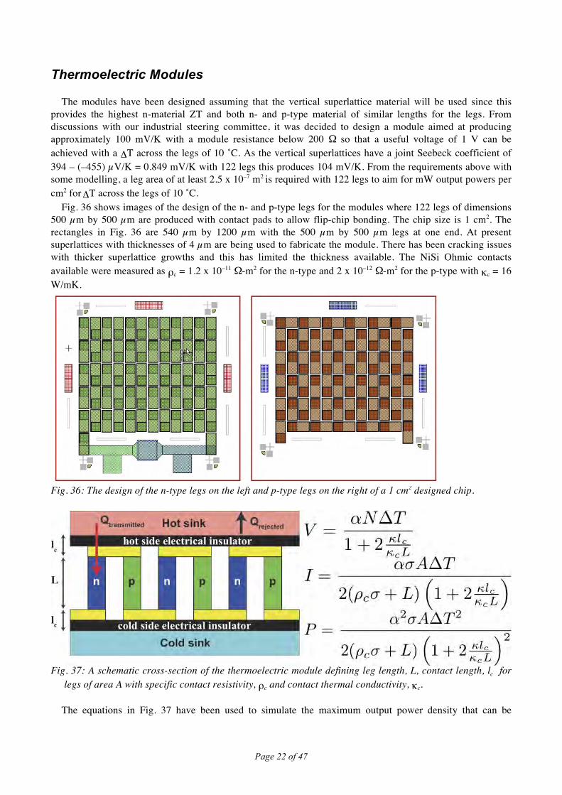
Thermoelectric Modules The modules have been designed assuming that the vertical superlattice material will be used since this
provides the highest n-material ZT and both n- and p-type material of similar lengths for the legs. From discussions with our industrial steering committee, it was decided to design a module aimed at producing approximately 100 mV/K with a module resistance below 200 Ω so that a useful voltage of 1 V can be achieved with a ΔT across the legs of 10 ˚C. As the vertical superlattices have a joint Seebeck coefficient of 394 – (–455) µV/K = 0.849 mV/K with 122 legs this produces 104 mV/K. From the requirements above with some modelling, a leg area of at least 2.5 x 10⁻⁷ m2 is required with 122 legs to aim for mW output powers per cm2 for ΔT across the legs of 10 ˚C.
Fig. 36 shows images of the design of the n- and p-type legs for the modules where 122 legs of dimensions 500 µm by 500 µm are produced with contact pads to allow flip-chip bonding. The chip size is 1 cm2. The rectangles in Fig. 36 are 540 µm by 1200 µm with the 500 µm by 500 µm legs at one end. At present superlattices with thicknesses of 4 µm are being used to fabricate the module. There has been cracking issues with thicker superlattice growths and this has limited the thickness available. The NiSi Ohmic contacts available were measured as ρc = 1.2 x 10⁻¹¹ Ω-m2 for the n-type and 2 x 10–12 Ω-m2 for the p-type with κc = 16 W/mK.
Fig. 36: The design of the n-type legs on the left and p-type legs on the right of a 1 cm2 designed chip.
Fig. 37: A schematic cross-section of the thermoelectric module defining leg length, L, contact length, lc for
legs of area A with specific contact resistivity, ρc and contact thermal conductivity, κc.
The equations in Fig. 37 have been used to simulate the maximum output power density that can be
Page 23 of 47
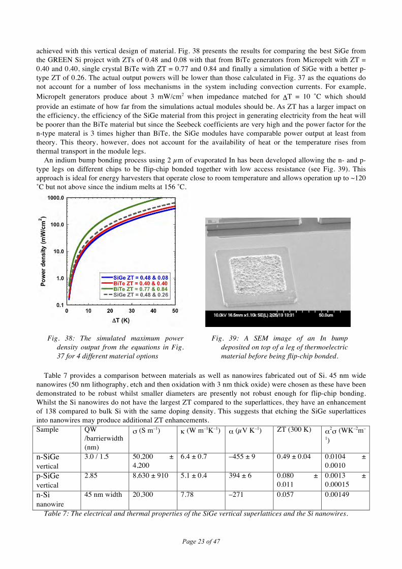
achieved with this vertical design of material. Fig. 38 presents the results for comparing the best SiGe from the GREEN Si project with ZTs of 0.48 and 0.08 with that from BiTe generators from Micropelt with ZT = 0.40 and 0.40, single crystal BiTe with ZT = 0.77 and 0.84 and finally a simulation of SiGe with a better p-type ZT of 0.26. The actual output powers will be lower than those calculated in Fig. 37 as the equations do not account for a number of loss mechanisms in the system including convection currents. For example, Micropelt generators produce about 3 mW/cm2 when impedance matched for ΔT = 10 ˚C which should provide an estimate of how far from the simulations actual modules should be. As ZT has a larger impact on the efficiency, the efficiency of the SiGe material from this project in generating electricity from the heat will be poorer than the BiTe material but since the Seebeck coefficients are very high and the power factor for the n-type materal is 3 times higher than BiTe, the SiGe modules have comparable power output at least from theory. This theory, however, does not account for the availability of heat or the temperature rises from thermal transport in the module legs.
An indium bump bonding process using 2 µm of evaporated In has been developed allowing the n- and p-type legs on different chips to be flip-chip bonded together with low access resistance (see Fig. 39). This approach is ideal for energy harvesters that operate close to room temperature and allows operation up to ~120 ˚C but not above since the indium melts at 156 ˚C.
Table 7 provides a comparison between materials as well as nanowires fabricated out of Si. 45 nm wide
nanowires (50 nm lithography, etch and then oxidation with 3 nm thick oxide) were chosen as these have been demonstrated to be robust whilst smaller diameters are presently not robust enough for flip-chip bonding. Whilst the Si nanowires do not have the largest ZT compared to the superlattices, they have an enhancement of 138 compared to bulk Si with the same doping density. This suggests that etching the SiGe superlattices into nanowires may produce additional ZT enhancements. Sample QW
/barrierwidth (nm)
σ (S m–1) κ (W m–1K–1) α (µV K–1) ZT (300 K) α2σ (WK–2m–
1)
n-SiGe vertical
3.0 / 1.5 50,200 ± 4,200
6.4 ± 0.7 –455 ± 9 0.49 ± 0.04 0.0104 ± 0.0010
p-SiGe vertical
2.85 8,630 ± 910 5.1 ± 0.4 394 ± 6 0.080 ± 0.011
0.0013 ± 0.00015
n-Si nanowire
45 nm width 20,300 7.78 –271 0.057 0.00149
Table 7: The electrical and thermal properties of the SiGe vertical superlattices and the Si nanowires.
Fig. 38: The simulated maximum power density output from the equations in Fig. 37 for 4 different material options
Fig. 39: A SEM image of an In bump deposited on top of a leg of thermoelectric material before being flip-chip bonded.

Page 24 of 47
Fig. 40 shows images of the fabricated n- and p-type legs for the modules where 122 legs of dimensions
500 µm by 500 µm were produced with contact pads to allow flip-chip bonding. Also on the same mask but still to be deposited are the Al interconnects and the Al pads to make up the capacitor. Finally there is a resistor that will act as a thermometer for the sensor that is to be powered by the output from the thermoelectric harvesters. The rectangles in Fig. 4.5 are 540 µm by 1200 µm with the 500 µm by 500 µm legs at one end. The indium bump bonding process was used to flip-chip bond the n- and p-type legs on different chips to each other. Finally a capacitor with an area of 1 µm2 and 100 nm of Si3N4 as the dielectric has been designed to have a capacitance of ~ 664 pF to store the generated charge and thermometers have been integrated as sensors to allow the ΔT to be determined across the legs.
Fig. 40: Left: An optical microscope images of the fabricated design of the n-type legs for the module before
they are flip-chip bonded together using an indium bump bonding process. The device is ~1 cm2. Right: An optical microscope image of the p-type legs before flip-chip bonding.
Fig. 41 and Fig. 42 demonstrate the Seebeck voltage and the power density respectively from the completed
module. The voltages and powers are quite small and are related to a number of issues in this first attempt at a complete module demonstrator. The first is that both the n- and the p-type material are grown on graded buffer
Fig. 41: The Seebeck voltage as a function of ΔT across the module with the cold sink at ~300 K.
Fig. 42: The power density as a function of ΔT across the module with the cold sink at ~ 300 K.
Page 25 of 47
layers which do not provide a high level of electrical isolation to the substrate. The Seebeck voltage measured is too small indicating that either the ΔT across the legs is not correct or that there is parallel electrical conduction rather than serial through the legs due to the lack of electrical substrate isolation. If one calculates the expected Seebeck voltage by considering the legs electrically in parallel (i.e. with no electrical isolation to the substrate) then the expected Seebeck coefficient over 122 legs is 0.028 µV/K rather than 849 µV/K when in series (i.e. with electrical isolation to the substrate). The actual value is ~70 µV/K suggesting there is some electrical isolation to the substrate but this is not complete. The thick ~15 µm graded Si1-yGey buffer provides a low thermal conductivity connection between the legs and the hot source and the cold sink. This provides a poor thermal resistance to the legs of the module and the hot source and the cold sink. Therefore the temperature drop across the legs is not optimal and indeed the ΔT was measured between the backs of the two flip-chip bonded wafers and therefore may not directly correspond to the ΔT across the legs. Finally the legs of the module are only 4 µm long which potentially allows significant convection currents that may reduce the ΔT across the legs.
The effective ZT for the module is given by !" = !!!!!
!!
!!!!! !!
!!
which for the data in Table 7 gives a ZT of
0.061. It is clear that the p-type ZT is dominating the module performance and improvements will require much more work on the p-type material than the n-type. Also the legs have not yet been balanced for the difference in generation. This requires the Peltier and Fourier effects to be balanced for both legs which results
for legs of length L and area A to be !!!!!!!!
= !!!!!!!!
and so with the data in table 1, the p-legs should have an
area 2.7 times larger than the n-type material legs for legs of the same length. Two new wafers based on the same superlattices as those in Table 7 but with thin ~1 µm SiGe buffers
grown on top of SOI substrates with 10 µm thick superlattices have been grown by Polimi and now delivered to UGLA. The SOI should provide electrically insulating substrates (the legs will be etched to the oxide for complete electrical isolation to the substrate and between the legs to guarantee serial electrical conduction when the module is flip-chip bonded), the thin SiGe buffers should reduce the thermal resistance and the thicker superlattices should reduce convection currents. These were not available early enough for the final report but fabrication will continue after the project and it is hoped that a better module demonstration with higher output powers along with the capacitor and the powering of the sensor can be achieved by the review meeting in September.

Page 26 of 47
4.1.4 The potential impact (including the socio-economic impact and the wider societal implications of the project so far) and the main dissemination activities and exploitation of results
When the GREEN Silicon proposal was written 4 years ago, renewable energy was a hot topic with research funds being placed to improve both the efficiency and output power from renewable sources. At that stage renewable energy sources produce very little electrical output power compared to conventional coal, oil, gas and nuclear power generation. This position has not changed significantly and there have not been significant improvements in the low levels of output powers available from renewable sources compared to conventional generation. This is especially true of thermoelectric materials and generators. There has, however, been improvements with thermoelectric generation especially with a range of new sustainable materials demonstrating comparable performance to the conventional unsustainable materials and improved fabrication has increased the output powers. For thermoelectrics, the majority of the potential impacts of improved thermoelectric performance stated in the GREEN Silicon proposal still hold although there have been a number of changes. The thermodynamic conversion efficiency of thermoelectrics is still limited to ≤ 5% and n-Bi2Te3 and p-Sb2Te3 are still the dominant thermoelectric materials being used in complete generator systems. This is despite the issues with tellurium being the 9th rarest element on planet earth which is driving research to look for sustainable thermoelectric materials. Whilst even more nanostructured thermoelectric materials have been produced (see Fig. 43), none of the nanostructured materials with ZT > 1 have been reproduced by more than an individual research group. Also no thermoelectric generators have been produced with the nanostructured materials. There is a growing level of suspicion by the thermoelectric community that many of these high ZT results are not correct. Hence in the GREEN Silicon project we spent a substantial amount of time checking that our measurements had low uncertainties and collaborated with NPL and the University of Illinois to cross check our measurements especially for thermal conductivity.
Fig. 43: The n-type (left) and p-type (right) ZT values from the recent literature compared to the GREEN Silicon results. None of the literature results on nanostructured materials with ZT > 1 have been reproduced and none of the materials have been fabricated into a generator. The n-type Ge/SiGe superlattice results that have been produced in GREEN Silicon have the highest ZT and power factors reported in the literature for tellurium-free material between room temperature and 100 ˚C. The GREEN Silicon project has also demonstrated that these nanostructured materials can be microfabricated into

Page 27 of 47
complete thermoelectric generators and the project has demonstrated electrical output power. Whilst the initial output powers are modest, it is clear from simulations and modelling that with further research and development to optimise both the materials and the generator design that significantly higher output powers can be produced from the microfabricated SiGe thermoelectric generators developed in GREEN Silicon. Indeed the powers should be greater than the present BiTe-alloy devices for suitably optimised systems. Therefore the GREEN Silicon project has made impact in the thermoelectrics community by producing the highest performance Te-free thermoelectric material at room temperature and the first thermoelectric generators with complete nanostructured n- and p-type material. Societal Impacts The societal benefits and potential impacts will now be discussed. Building automation involves the use of a distributed control system to improve performance of the building as a whole. It utilises an intelligent network of electronic devices to monitor and control aspects of the building such as lighting, heating and ventilation. It also includes sensing for smart use of appliances. Such intelligent networks enable the optimisation of energy use and therefore lower total operating costs of buildings. This sector has been one of the most enthusiastic adopters of wireless solutions and the incorporation of energy harvesting as an alternative to battery power. This has been greatly helped by the existence of a compelling use case for both wireless and energy harvesting, and the growth in use of standard ultra low power wireless platforms, driven largely by EnOcean (a German company). The case for energy harvesting in building automation is therefore well established and supply chains are already in place with hundreds of products and many tens of thousands of buildings having installations. With the building industry being generally rather conservative the main successes have been in commercial buildings with significant interest in energy efficiency. There is therefore still significant scope to widen awareness of the potential of the technology. The many existing use cases make this less about technology development and more about demonstrating benefit in more situations. Particularly in large buildings the main driver for wireless sensing in building automation is the avoidance of large amounts of wiring. This has benefits in installation time and labour and material costs but also allows easy reconfiguration, particularly in commercial buildings. For example, installing occupancy sensors that turn off lights in vacant rooms can save up to 40 percent on energy and operating costs. The argument for energy harvesting over battery power is largely down to the sheer number and therefore cost and inconvenience of battery change. Future scenarios for building automation suggest an even greater trend towards embedded sensing devices that would make battery change even less of an option. The number of batteries that would be required to power wireless devices in building automation would also present a major environmental issue with disposal. Thermoelectrics are one technology along with photovoltaics (PV) that are being investigated for energy harvesting in the building environment. The thermoelectrics have the advantage of being able to run for 24 hours a day compared with the limited time for PV but only when temperature differences greater than 10 ˚C are available. Boilers and radiators in buildings are ideal heat sources to power thermoelectric energy harvesters.
In one example quoted by EnOcean 4200 wireless and batteryless light switches, occupancy sensors and daylight sensors were installed in a new building construction in Madrid. These are powered by energy harvesters and embedded in the building. This saved 40% of lighting energy costs by automatically controlling the lighting in the building, removed the need for 20 miles of cables, avoided the use and changing of 42,000 batteries (over 25 years) and saved 80% of the cost of retrofitting a wired solution.
With an ageing population, people are increasingly living longer whilst managing chronic diseases e.g. diabetes and heart disease. There is therefore a trend towards pervasive health monitoring and shifting this from the hospital to the home due to the need to reduce healthcare costs and at the same time expand provision. This means the adoption of a wide range of diagnostic and monitoring sensors, drug delivery patches and even tracking devices and alarms for vulnerable patients. Whilst these could be battery powered the sheer numbers of them and the environmental implications of battery disposal as well as a preference for

Page 28 of 47
not having patients changing batteries means that energy harvesting could potentially be a key enabling technology. There are also a number of implanted medical devices that are necessarily already wireless and therefore currently battery powered. In these battery change requires a surgical procedure e.g. heart pacemakers.
It is envisaged that the development of simple, reliable and affordable devices may through continuous monitoring enable: • Point of care diagnostics • Telemonitoring • Chronic disease self-management • Delivery of personalised healthcare • New insights into disease progression • Post operative recovery monitoring away from the hospital
General requirements are that the devices and any body area network (BAN) should be non-intrusive in terms of both use and maintenance, low cost and provide a useful rate of information provision to patients to allow for improved quality of life and to doctors in case of critical health issues. Whilst it is likely that batteries could power these devices there is some argument for avoiding the need to change batteries or the environmental impact if such sensing were to proliferate as a disposable option. Energy harvesting such as thermoelectrics is not critical to the application but would add value.
Hearing aids (discussed above) are an example of an application where energy harvesting would be desirable from a convenience and potentially cost perspective. Currently most of these are wearable devices although implantable ones also exist. The batteries in many hearing aids require frequent replacement and many of the users forget to stock replacements.
The automotive sector is presently the sole area looking at thermoelectric energy harvesting as a major technology that can improve the fuel efficiency by removing the kinetic load on the engine from the alternator. New European pollution legislation for cars is driving companies to look for energy harvesting solutions to improve fuel efficiency. This sector is aiming for kW generation from thermoelectrics which is orders of magnitude greater than the output powers required by the remaining sensor application fields and is strictly speaking energy harvesting at a much larger scale than the level being pursued by the GREEN Silicon project under the EC FET Towards Zeropower ICT. From discussions with many industrial parties, it is clear that the GREEN Silicon technology if developed further for high temperature operation (up to 500 ˚C) could have significant applications for the automotive sector. This is mainly because the two main alloys for automotive thermoelectrics using the rare and unsustainable tellurium element and the toxic and therefore banned lead (Bi(Sb)Te and PbTe alloys are the main thermoelectric materials at present).
The two key issues for the automotive applications are output power and cost. With 65% of the energy in
the fuel being lost as heat, there is enormous potential to capture parts of this heat and at least augment the electrical generation from the alternator as thermoelectrics are presently unlikely to generate sufficient electricity to be the complete solution for electricity generation. At motorway speeds there is 10s of kWs available in heat with exhaust temperature ≥ 500 ˚C potentially allowing thermodynamic conversion efficiencies up to 10% but for city journeys far less heat at lower temperatures is available. Therefore removing the alternator completely is not yet a viable solution with present thermoelectric efficiencies. The major problem in achieving high output powers is how to capture the heat from the exhaust whilst simulatanelously maintaining the cold side temperature. Therefore, a high power factor is more important than the conversion efficiency (ZT) for the thermoelectric materials since the heat is plentiful and only a fraction will be harvested by any device. Substantial work is to be done if thermoelectrics are to become standard in the automotive sector but legislation and increasing fuel costs are providing commercial drivers for the technology. Thermoelectrics are also being developed to power sensor nodes on vehicles especially close to the engine and transmission systems where substantial temperature differences are available.

Page 29 of 47
In most of the applications sectors examined above there is a clear drive towards the adoption of wireless sensing technologies. The extent of engagement with the technology varies though by sector, not least because wireless sensor networks are still generally in the early stages of commercial deployment and are therefore not yet fit for purpose in many applications. Some sectors tend to drive the exploration of both wireless sensing and of energy harvesting as a power source whilst others are followers and will benefit from advances made elsewhere.
Whilst wireless sensing is clearly needed in all of the application sectors, the case for using energy
harvesting to power them varies considerably. In some cases the sensing application is only really viable if an alternative to battery power is possible. In others the argument for energy harvesting is less critical in terms of performance of the system and would therefore need to be made in consideration of the environmental issue of a massive proliferation of battery use or just the general convenience of not having to change batteries. Of course in many wireless sensing applications there are currently no energy harvesters capable of supplying sufficient power for the duration required. This situation may change as energy harvesters are improved and power requirements of the sensing systems is reduced. In fact, a major area of focus should be on optimising the power needs of sensing systems as these have rarely been designed with power use considerations in mind. Finally, some applications will never be possible with energy harvesting due to high power requirements and/or extremely challenging operational environments.
In general, therefore, it is necessary to examine the particular use cases in a sector to understand whether or not the drive for wireless sensing is particularly strong. It is also necessary to understand the difference in each case between energy harvesting being a necessity and it being a convenience which the industry concerned does not place sufficient value at present. As always this situation may well evolve as technology, requirements and the value put on capabilities changes. Therefore whilst thermoelectrics will have clear impacts for society for automotive, building automation, healthcare automotive and a number of other areas with clear benefits towards lowering pollution and improving quality of life by providing point-of-care healthcare, the real level of impact on society will not be understood and quantifiable until 10 to 20 years time. Dissemination Europe has a significant number of companies involved in thermoelectric generation and Peltier cooling. When the supply chain of materials, fabrication and users is added to the thermoelectric companies, the number of EC companies involved with thermoelectrics at any level grows into the hundreds. The GREEN Silicon project has been involved in discussions with a range of EC based companies with an aim of exploiting the research results. The co-ordinator met has met with European Thermodynamics (U.K. SME), Johnson-Matthey (U.K.), Semefab (U.K.) and IQE (U.K.) to discuss exploitation of the results from GREEN Silicon. The co-ordinator has also had discussions with end users of the technology including Jaguar Land-Rover (U.K.) and Rolls-Royce (U.K.) about the thermoelectric requirements for applications. In addition Prof Paul and Dr Isella met with the EC project NanoHiTEC and their partners from the German companies O-flexx and Oerlikon. Fiat (Italy) is also a partner in the project. UGLA has a UK funded project with European Thermodynamics that has the aim of exploiting some of the knowledge from the GREEN Silicon project to an EC SME. GREEN Silicon will supply some material from the project to O-flexx to test the performance of the material in one of their thermoelectric modules. Therefore some of the results from the GREEN Silicon project have been directly transferred by dissemination to EC companies for potential exploitation. Also in September 2013, GREEN Silicon is presenting the results from the project at a workshop with all the FP7 funded thermoelectrics projects. The GREEN Silicon project has also disseminated the results through its public web pages, by publishing 20 papers in peer reviewed journals and by giving 29 presentations at a range of conferences and workshops. Also there are a further 3 papers in preparation at present. A full list of publications and presentations is presented in section 4.2 part A.

Page 30 of 47
4.1.5 Address of the project public website, and relevant contact details.
http://www.greensilicon.eu/GREENSilicon/index.html Contact details: UGLA: Prof Douglas J. Paul, E-mail: [email protected], Tel: +44 141 330 5219 POLIMI: Dr Giovanni Isella, E-mail: [email protected], Tel: +39 031 332 7303 JKU: Dr Julien Stangl, E-mail: [email protected], Tel: +43 732 2468 9604 ETH Zurich: Dr Elisabeth Müller Gubler, E-mail: [email protected], [email protected], Tel: +41 56 310 5411

Page 31 of 47
4.2 Use and dissemination of foreground Section A (public)
TEMPLATE A1: LIST OF SCIENTIFIC (PEER REVIEWED) PUBLICATIONS, STARTING WITH THE MOST IMPORTANT ONES
NO. Title Main
author
Title of the periodical or the series
Number, date or
frequency Publisher
Place of publication
Year of publication
Relevant pages
Permanent identifiers1
(if available)
Is/Will open access2
provided to this
publication?
1 The thermoelectric properties of Ge/SiGe modulation doped superlattices
A. Samarelli et al.
J. Appl. Phys. 113 AIP Journal 2013 233704 DOI: 10.1063/1.4811228 Yes
2 A study of the impact of dislocations on the thermoelectric propoerties of quantum wells in the Si/SiGe materials system
J.R. Watling and D.J. Paul
J. Appl. Phys.
110
AIP Journal 2011
114508
DOI: 10.1063/1.3665127 Yes
3 The cross-plane thermoelectric properties of p-Ge/Si0.5Ge0.5 superlattices
A. Samarelli et al.,
Appl. Phys. Lett.
Accepted for publication
AIP Journal 2013
Yes
4 Ohmic contacts to n-type germanium with low specific contact resistivity
K. Gallacher et al.
Appl. Phys. Lett.
100
AIP Journal 2012
022113
DOI: 10.1063/1.3676667 Yes
5 Ge/SiGe superlattices for nanostructured thermoelectric modules
D. Chrastina et al.
Thin Solid Films
543
Elsevier Journal 2013
pp. 153 - 156
DOI: 10.1016/j.tsf.2013.01.002
Yes
6 Prospects for SiGe A. Solid State Submitted Elsevier Journal 2013 Yes
1 A permanent identifier should be a persistent link to the published version full text if open access or abstract if article is pay per view) or to the final manuscript accepted for publication (link to article in repository). 2 Open Access is defined as free of charge access for anyone via Internet. Please answer "yes" if the open access to the publication is already established and also if the embargo period for open access is not yet over but you intend to establish open access afterwards.

Page 32 of 47
Thermoelectric Generators Samarelli et al.
Electronics
7 Power Factor Characterization of Ge/SiGe Thermoelectric Superlattices at 300 K
A. Samarelli et al.
J. Elec. Mat.
42
Springer Journal 2013 pp. 1449 – 1453
DOI: 10.1007/s11664-012-2287-z
Yes
8 Thermal Conductivity Measurement Methods for SiGe Thermoelectric Materials
L. Ferre Llin et al.
J. Elec. Mat.
42
Springer Journal 2013 pp. 2376 – 2380
DOI: 10.1007/s11664-013-2505-3-z
Yes
9 Ge/SiGe Superlattices for Thermoelectric Devices Grown by Low-Energy Plasma-Enhanced Chemical Vapor Deposition
S. Cecchi et al.
J. Elec. Mat.
42
Springer Journal 2013
pp. 2030 – 2034
DOI: 10.1007/s11664-013-2511-5
Yes
10 Ge/SiGe superlattices for thermoelectric energy conversion devices
S. Cecchi et al.
J. Mat. Sci.
48
Springer Journal 2013 pp. 2829 - 2835
DOI: 10.1007/s10853-012-6825-0
Yes
11 Nanofabrication of high aspect ratio (~50:1) sub-10 nm silicon nanowires using plasma etch technologies
M. Mirza et al.
J. Vac. Sci. Technol. B
30
AVS Journal 2012
06FF02
DOI: 10.1116/1.4755835 Yes
12 Si/SiGe Thermoelectric Generators
D. J. Paul et al.
Electrochem. Soc. Trans. 50(9)
ECS Journal 2012 pp. 959 - 963
doi:10.1149/05009.0959ecst
Yes
13 Low Specific Ohmic Contacts to n-type Germanium Using a Low Temperature NiGe Process
K. Gallacher et al.
Electrochem. Soc. Trans.
50(9)
ECS Journal 2012 pp. 1081 - 1084
doi:10.1149/05009.1081ecs
Yes
14
Prospects for SiGe thermoelectric generators
D.J. Paul et al.
Proc. 14th International Conference on Ultimate Integration on Silicon
IEEE Conference proceedings
2013
pp. 5-8
DOI: 10.1109/ULIS.2013.6523478
Yes
15
Si/SiGe Nanoscale Engineered Thermoelectric Materials for Energy Harvesting
D.J. Paul et al.
Proceedings of the IEEE International Conference on Nanotechnology 2012
IEEE Conference proceedings
2012
pp. 7913 - 7917
doi 10.1109/NANO.2012.6322044
Yes
16 Controlling the polarization dynamics by strong THz fields in photoexcited germanium
N. Koester et al.
New J. Phys.
15
IOP PUBLISHING LTD
Journal 2013
075004
DOI: 10.1088/1367-2630/15/7/075004
Yes

Page 33 of 47
quantum wells 17 Strong quantum-confined
Stark effect from light hole related direct-gap transitions in Ge quantum wells
P. Chaisakul et al.
Appl. Phys. Lett.
102
AIP Journal 2013
191107
DOI: 10.1063/1.4805004
Yes
18 Electro-refractive effect in Ge/SiGe multiple quantum wells
J. Frigerio et al.
Appl. Phys. Lett
102
AIP Journal 2013
061102
DOI: 10.1063/1.4792271
Yes
19 Dephasing in Ge/SiGe quantum wells measured by means of coherent oscillations
K. Kolata et al.
Phys. Rev. B
86
AIP Journal 2012
201303
DOI: 10.1103/PhysRevB.86.201303
Yes
20 Quantum-confined Stark effect at 1.3 µm in Ge/Si0.35Ge0.65 quantum-well structure
M. S. Rouifed et al.
Optics Letters
37
OSA Journal 2012
3960-3962
Yes

Page 34 of 47
TEMPLATE A2: LIST OF DISSEMINATION ACTIVITIES
NO. Type of activities3 Main leader
Title Date/Period Place Type of audience4
Size of audience
Countries addressed
1 Conference D.J. Paul GREEN Si 2013 Perugia, Italy
Scientific 50 EC & International
2 Workshop - Zeropower Summer School
D.J. Paul Introduction to harvesting thermal energy
2013 Perugia, Italy
Scientific PhD students
30 EC & International
3 Workshop - Meeting with Industrial partners of EC NanoTEC project
D.J. Paul & G. Isella
GREEN Silicon project 2013 Zurich, Switzerland
Industry 7 EC (Germany, Italy, Austria, Switzerland, U.K.)
4 Conference – ULIS 2013 D.J. Paul Prospects for SiGe Thermoelectric Generators
2013 Warwick, U.K.
Scientific 200 EC & International
5 Conference - Proceedings of the IEEE International Conference on Nanotechnology 2012
D.J. Paul Si/SiGe Nanoscale Engineered Thermoelectric Materials for Energy Harvesting 2012
Birmingham, U.K.
Scientific
200
EC & International
6 Conference - Proceedings of the IEEE International Conference on Nanotechnology 2012
D.J. Paul Silicon Nanowire Devices with Widths Below 5 nm
2012
Birmingham, U.K.
Scientific
200
EC & International
7 Conference - 31st International and 10th European Conference on Thermoelectrics
A. Samarelli
Si/SiGe Heteroepitaxial materials for
Thermoelectric Applications 2012
Aarbourg, Denmark
Scientific
200
EC & International
8 Conference - 31st International L. Ferre Accurate Measurements 2012 Aarbourg, Scientific 200 EC &
3 A drop down list allows choosing the dissemination activity: publications, conferences, workshops, web, press releases, flyers, articles published in the popular press, videos, media briefings, presentations, exhibitions, thesis, interviews, films, TV clips, posters, Other. 4 A drop down list allows choosing the type of public: Scientific Community (higher education, Research), Industry, Civil Society, Policy makers, Medias, Other ('multiple choices' is
possible).

Page 35 of 47
and 10th European Conference on Thermoelectrics
Llin of Thermal Conductivity of SiGe Thermoelectric
Materials
Denmark International
9
Conference - 31st International and 10th European Conference on Thermoelectrics
S. Cecchi Ge/SiGe Superlattices for Thermoelectric Devices Grown by Low-Energy
Plasma-Enhanced Chemical Vapor
Deposition 2012
Aarbourg, Denmark
Scientific
200
EC & International
10 Conference – ECS PRIME
D.J. Paul Si/SiGe Thermoelectric Generators 2012
Honolulu, USA
Scientific 200
International
11
Conference – ECS PRIME
D.J. Paul Low Specific Ohmic Contacts to n-type
Germanium Using a Low Temperature NiGe
Process 2012
Honolulu, USA
Scientific
200
International
12 Workshop - 2nd Thomas-Young Centre Energy Materials Workshop And Tutorial
D.J. Paul Thermoelectric Energy Harvesting
2012
London, U.K.
Scientific
100
EC & International
13 Workshop - International School on Statistical Physics at Ettore Majorana Centre
D.J. Paul Advances on Thermoelectrics Energy
Harvesting 2012
Erice, Italy Scientific
50
EC & International
14 Workshop - Zeropower
D.J. Paul GREEN Silicon 2012
Barcelona, Spain
Scientific 60
EC
15
Workshop - Zeropower
S. Cecchi The growth of Ge/SiGe superlattices for thermoelectric applications 2012
Barcelona, Spain
Scientific
60
EC
16
Workshop - Zeropower
L. Ferre Llin
Accurate measurement of thermal conductivity and
ZT of thermoelectric heterostructures 2012
Barcelona, Spain
Scientific
60
EC
17
Conference - EMRS
S. Cecchi Ge/SiGe superlattices for thermoelectric devices grown by LEPECVD 2012
Strasbourg, France
Scientific
500
EC
18
Conference - NanoSEA
D. Chrastina
Ge/SiGe superlattices for nanostructured
thermoelectric modules 2012
Sardinia, Italy
Scientific
100
International
19
Conference - EIPBN
M. Mirza Nanofabrication of high aspect ratio (~50:1) sub-10 nm silicon nanowires 2012
Waikoloa, USA
Scientific
600
International

Page 36 of 47
using plasma etch technologies
20 Industry Trade Show – IDTechEX
D.J. Paul Si/SiGe Microfabricated Thermoelectric Materials,
Devices and Modules 2013
San Jose, USA
Trade Show
2000
International
21 Science Outreach Events to Schools
D.J. Paul Energy: Can renewables save the planet 2012
Glasgow, U.K.
Schools 120
U.K.
22 Workshop – UK Energy Harvesting Network
D.J. Paul Microfabricated Thermoelectric Devices on Silicon Substrates 2013
London, U.K.
Industry
100
EU
23
Workshop
D.J. Paul SiGe thermoelectric materials
2011
NPL, Teddington, U.K.
Scientific Metrology
25
U.K.
24 Workshop - Zeropower Summer School
D.J. Paul Introduction to thermoelectrics
2011
Perugia, Italy
Scientific PhD students 40
EU & International
25 Workshop - Zeropower Workshop
S. Cecchi Ge/SiGe Superlattices for Thermoelectric Applications 2011
Perugia, Italy
Scientific PhD students 40
EU & International
26 Workshop - Zeropower Workshop
F. Isa SiGe heterostructures for optoelectronics applications 2011
Perugia, Italy
Scientific PhD students 40
EU & International
27 Workshop - Zeropower Summer School
D.J. Paul Thermoelectric energy harvesting
2010
Avigliano Umbro, Italy
Scientific PhD students 40
EU & International
28 Workshop - CECAM A. Samarelli
Thermal and Electrical Characterisation of Ge/SiGe thermoelectric materials 2013
Lausanne, Switzerland
Scientific
40
EU & International
29 Workshop – EC NANO4TE A. Samarelli
The GREEN Silicon Project 2013
Warsaw, Poland
Scientific 40
EU

Page 37 of 47
Section B (Confidential) Part B1
TEMPLATE B1: LIST OF APPLICATIONS FOR PATENTS, TRADEMARKS, REGISTERED DESIGNS, ETC.
Type of IP Rights5:
Confidential Click on YES/NO
Foreseen embargo date dd/mm/yyyy
Application reference(s)
(e.g. EP123456) Subject or title of application
Applicant (s) (as on the application)
none
5 A drop down list allows choosing the type of IP rights: Patents, Trademarks, Registered designs, Utility models, Others.

Page 38 of 47
Part B2 Please complete the table hereafter:
Type of Exploitable Foreground6
Description of
exploitable foreground
Confidential Click on YES/NO
Foreseen embargo
date dd/mm/yyyy
Exploitable product(s) or measure(s)
Sector(s) of application7
Timetable, commercial or any other use
Patents or other IPR exploitation (licences)
Owner & Other Beneficiary(s) involved
High ZT n-type SiGe thermoelectric material designs
knowledge
Yes
January 2014
High ZT n-type SiGe thermoelectric material
Energy Harvesting
2015+
A materials patent application is planned for 2013
Beneficiary UGLA (owner) Poss. licensing to EC companies European Thermodynamics and O-flexx.
• UGLA is looking to make a patent declaration of the n-type SiGe thermoelectric material designs which resulted in the high ZT results with
the aim of moving to a patent filing. Interest has already been shown by European Thermodynamics and O-flexx to use this technology. The material has the potential to replace PbTe for automotive energy harvesting applications. If successfully adopted then the potential impact could be large by aiding the reduction of pollution from automotive vehicles.
19 A drop down list allows choosing the type of foreground: General advancement of knowledge, Commercial exploitation of R&D results, Exploitation of R&D results via standards, exploitation of results through EU policies, exploitation of results through (social) innovation. 7 A drop down list allows choosing the type sector (NACE nomenclature) : http://ec.europa.eu/competition/mergers/cases/index/nace_all.html

Page 39 of 47
4.1 Report on societal implications Replies to the following questions will assist the Commission to obtain statistics and indicators on societal and socio-economic issues addressed by projects. The questions are arranged in a number of key themes. As well as producing certain statistics, the replies will also help identify those projects that have shown a real engagement with wider societal issues, and thereby identify interesting approaches to these issues and best practices. The replies for individual projects will not be made public.
A General Information (completed automatically when Grant Agreement number is entered.
Grant Agreement Number: 257750
Title of Project: Generate Renewable Energy Efficiently Using Nanofabricated
Cilison Name and Title of Coordinator: Prof Douglas J. Paul
B Ethics
1. Did your project undergo an Ethics Review (and/or Screening)? • If Yes: have you described the progress of compliance with the relevant Ethics
Review/Screening Requirements in the frame of the periodic/final project reports? Special Reminder: the progress of compliance with the Ethics Review/Screening Requirements should be described in the Period/Final Project Reports under the Section 3.2.2 'Work Progress and Achievements'
No
2. Please indicate whether your project involved any of the following issues (tick box) :
Yes
RESEARCH ON HUMANS • Did the project involve children? No • Did the project involve patients? No • Did the project involve persons not able to give consent? No • Did the project involve adult healthy volunteers? No • Did the project involve Human genetic material? No • Did the project involve Human biological samples? No • Did the project involve Human data collection? No
RESEARCH ON HUMAN EMBRYO/FOETUS • Did the project involve Human Embryos? No • Did the project involve Human Foetal Tissue / Cells? No • Did the project involve Human Embryonic Stem Cells (hESCs)? No • Did the project on human Embryonic Stem Cells involve cells in culture? No • Did the project on human Embryonic Stem Cells involve the derivation of cells from Embryos? No
PRIVACY • Did the project involve processing of genetic information or personal data (eg. health, sexual
lifestyle, ethnicity, political opinion, religious or philosophical conviction)? No
• Did the project involve tracking the location or observation of people? No RESEARCH ON ANIMALS
• Did the project involve research on animals? No • Were those animals transgenic small laboratory animals? No • Were those animals transgenic farm animals? No

Page 40 of 47
• Were those animals cloned farm animals? No • Were those animals non-human primates? No
RESEARCH INVOLVING DEVELOPING COUNTRIES • Did the project involve the use of local resources (genetic, animal, plant etc)? No • Was the project of benefit to local community (capacity building, access to healthcare, education
etc)? No
DUAL USE • Research having direct military use Yes • Research having the potential for terrorist abuse No
C Workforce Statistics 3. Workforce statistics for the project: Please indicate in the table below the number of
people who worked on the project (on a headcount basis). Type of Position Number of Women Number of Men
Scientific Coordinator 0 1 Work package leaders 1 2 Experienced researchers (i.e. PhD holders) 0 2 PhD Students 2 2 Other 3 2
4. How many additional researchers (in companies and universities) were recruited specifically for this project?
6
Of which, indicate the number of men:
4

Page 41 of 47
D Gender Aspects 5. Did you carry out specific Gender Equality Actions under the project?
¡ l
Yes No
6. Which of the following actions did you carry out and how effective were they? Not at all
effective Very
effective
q Design and implement an equal opportunity policy ¡ ¡ ¡ ¡ ¡ q Set targets to achieve a gender balance in the workforce ¡ ¡ ¡ ¡ ¡ q Organise conferences and workshops on gender ¡ ¡ ¡ ¡ ¡ q Actions to improve work-life balance ¡ ¡ ¡ ¡ ¡ ¡ Other:
7. Was there a gender dimension associated with the research content – i.e. wherever people were the focus of the research as, for example, consumers, users, patients or in trials, was the issue of gender considered and addressed?
¡ Yes- please specify
l No
E Synergies with Science Education
8. Did your project involve working with students and/or school pupils (e.g. open days, participation in science festivals and events, prizes/competitions or joint projects)?
l Yes- please specify – outreach talks to schools
¡ No
9. Did the project generate any science education material (e.g. kits, websites, explanatory booklets, DVDs)?
¡ Yes- please specify
l No
F Interdisciplinarity
10. Which disciplines (see list below) are involved in your project? l Main discipline8: Physical sciences l Associated discipline8: Electrical
engineering, electronics
l Associated discipline8: Chemical sciences
G Engaging with Civil society and policy makers 11a Did your project engage with societal actors beyond the research
community? (if 'No', go to Question 14) l Yes
11b If yes, did you engage with citizens (citizens' panels / juries) or organised civil society (NGOs, patients' groups etc.)?
l No ¡ Yes- in determining what research should be performed ¡ Yes - in implementing the research ¡ Yes, in communicating /disseminating / using the results of the project
8 Insert number from list below (Frascati Manual).

Page 42 of 47
11c In doing so, did your project involve actors whose role is mainly to organise the dialogue with citizens and organised civil society (e.g. professional mediator; communication company, science museums)?
l Yes
12. Did you engage with government / public bodies or policy makers (including international organisations)
¡ No l Yes- in framing the research agenda ¡ Yes - in implementing the research agenda ¡ Yes, in communicating /disseminating / using the results of the project
13a Will the project generate outputs (expertise or scientific advice) which could be used by policy makers?
¡ Yes – as a primary objective (please indicate areas below- multiple answers possible) l Yes – as a secondary objective (please indicate areas below - multiple answer possible) ¢ No
13b If Yes, in which fields?
Energy
Y
Information Society Public Health Research and Innovation Transport

Page 43 of 47
13c If Yes, at which level? ¡ Local / regional levels l National level l European level l International level
H Use and dissemination
14. How many Articles were published/accepted for publication in peer-reviewed journals?
19
To how many of these is open access9 provided? 0
How many of these are published in open access journals? 0
How many of these are published in open repositories? 19
To how many of these is open access not provided? 0
Please check all applicable reasons for not providing open access: q publisher's licensing agreement would not permit publishing in a repository q no suitable repository available q no suitable open access journal available q no funds available to publish in an open access journal q lack of time and resources q lack of information on open access q other10: ……………
15. How many new patent applications (‘priority filings’) have been made? ("Technologically unique": multiple applications for the same invention in different jurisdictions should be counted as just one application of grant).
0
16. Indicate how many of the following Intellectual Property Rights were applied for (give number in each box).
Trademark 0
Registered design 0
Other 0
17. How many spin-off companies were created / are planned as a direct result of the project?
0
Indicate the approximate number of additional jobs in these companies: 0
18. Please indicate whether your project has a potential impact on employment, in comparison with the situation before your project:
q Increase in employment, or n In small & medium-sized enterprises n Safeguard employment, or q In large companies q Decrease in employment, q None of the above / not relevant to the project q Difficult to estimate / not possible to quantify
19. For your project partnership please estimate the employment effect resulting directly from your participation in Full Time Equivalent (FTE = one person working fulltime for a year) jobs:
Indicate figure:
9 Open Access is defined as free of charge access for anyone via Internet. 10 For instance: classification for security project.

Page 44 of 47
Difficult to estimate / not possible to quantify
X
I Media and Communication to the general public
20. As part of the project, were any of the beneficiaries professionals in communication or media relations?
¡ Yes l No
21. As part of the project, have any beneficiaries received professional media / communication training / advice to improve communication with the general public?
¡ Yes l No
22 Which of the following have been used to communicate information about your project to the general public, or have resulted from your project?
n Press Release n Coverage in specialist press n Media briefing q Coverage in general (non-specialist) press q TV coverage / report q Coverage in national press n Radio coverage / report q Coverage in international press n Brochures /posters / flyers q Website for the general public / internet q DVD /Film /Multimedia n Event targeting general public (festival, conference,
exhibition, science café)
23 In which languages are the information products for the general public produced?
q Language of the coordinator n English q Other language(s) Question F-10: Classification of Scientific Disciplines according to the Frascati Manual 2002 (Proposed Standard Practice for Surveys on Research and Experimental Development, OECD 2002): FIELDS OF SCIENCE AND TECHNOLOGY 1. NATURAL SCIENCES 1.1 Mathematics and computer sciences [mathematics and other allied fields: computer sciences and other
allied subjects (software development only; hardware development should be classified in the engineering fields)]
1.2 Physical sciences (astronomy and space sciences, physics and other allied subjects) 1.3 Chemical sciences (chemistry, other allied subjects) 1.4 Earth and related environmental sciences (geology, geophysics, mineralogy, physical geography and
other geosciences, meteorology and other atmospheric sciences including climatic research, oceanography, vulcanology, palaeoecology, other allied sciences)
1.5 Biological sciences (biology, botany, bacteriology, microbiology, zoology, entomology, genetics, biochemistry, biophysics, other allied sciences, excluding clinical and veterinary sciences)
2 ENGINEERING AND TECHNOLOGY 2.1 Civil engineering (architecture engineering, building science and engineering, construction engineering,
municipal and structural engineering and other allied subjects) 2.2 Electrical engineering, electronics [electrical engineering, electronics, communication engineering and
systems, computer engineering (hardware only) and other allied subjects] 2.3. Other engineering sciences (such as chemical, aeronautical and space, mechanical, metallurgical and
materials engineering, and their specialised subdivisions; forest products; applied sciences such as

Page 45 of 47
geodesy, industrial chemistry, etc.; the science and technology of food production; specialised technologies of interdisciplinary fields, e.g. systems analysis, metallurgy, mining, textile technology and other applied subjects)
3. MEDICAL SCIENCES 3.1 Basic medicine (anatomy, cytology, physiology, genetics, pharmacy, pharmacology, toxicology,
immunology and immunohaematology, clinical chemistry, clinical microbiology, pathology) 3.2 Clinical medicine (anaesthesiology, paediatrics, obstetrics and gynaecology, internal medicine, surgery,
dentistry, neurology, psychiatry, radiology, therapeutics, otorhinolaryngology, ophthalmology) 3.3 Health sciences (public health services, social medicine, hygiene, nursing, epidemiology) 4. AGRICULTURAL SCIENCES 4.1 Agriculture, forestry, fisheries and allied sciences (agronomy, animal husbandry, fisheries, forestry,
horticulture, other allied subjects) 4.2 Veterinary medicine 5. SOCIAL SCIENCES 5.1 Psychology 5.2 Economics 5.3 Educational sciences (education and training and other allied subjects) 5.4 Other social sciences [anthropology (social and cultural) and ethnology, demography, geography
(human, economic and social), town and country planning, management, law, linguistics, political sciences, sociology, organisation and methods, miscellaneous social sciences and interdisciplinary , methodological and historical S1T activities relating to subjects in this group. Physical anthropology, physical geography and psychophysiology should normally be classified with the natural sciences].
6. HUMANITIES 6.1 History (history, prehistory and history, together with auxiliary historical disciplines such as
archaeology, numismatics, palaeography, genealogy, etc.) 6.2 Languages and literature (ancient and modern) 6.3 Other humanities [philosophy (including the history of science and technology) arts, history of art, art
criticism, painting, sculpture, musicology, dramatic art excluding artistic "research" of any kind, religion, theology, other fields and subjects pertaining to the humanities, methodological, historical and other S1T activities relating to the subjects in this group]
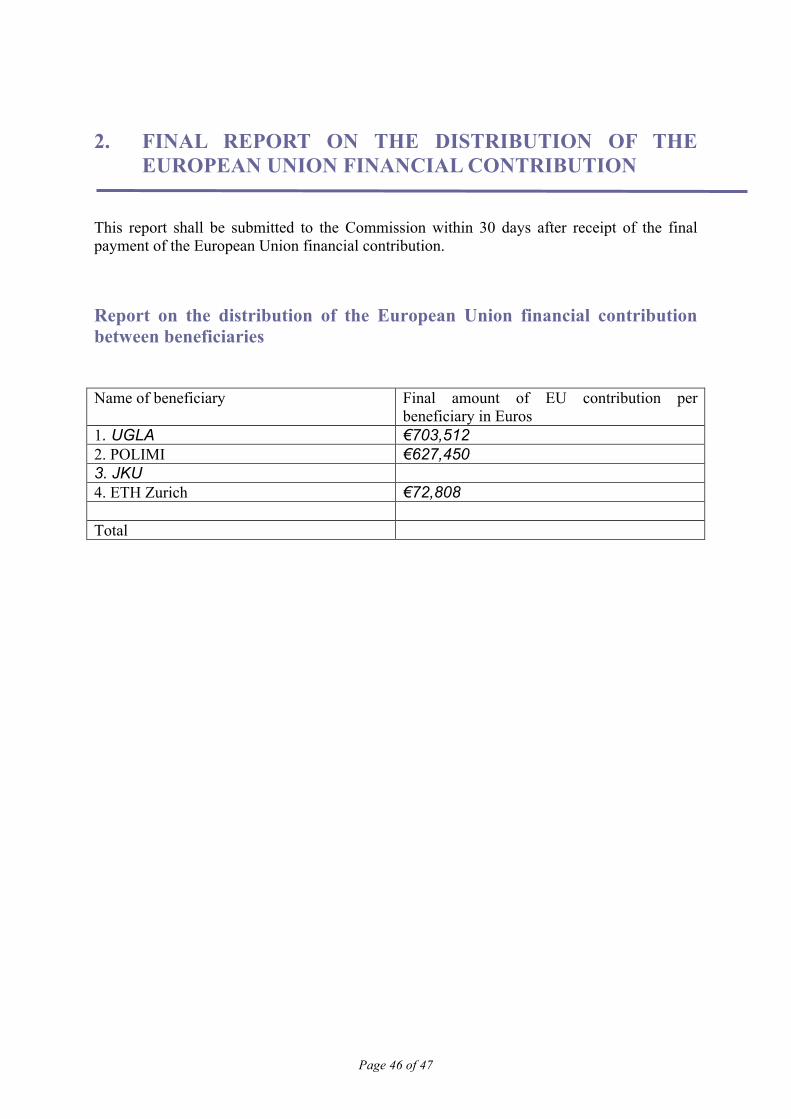
Page 46 of 47
2. FINAL REPORT ON THE DISTRIBUTION OF THE EUROPEAN UNION FINANCIAL CONTRIBUTION
This report shall be submitted to the Commission within 30 days after receipt of the final payment of the European Union financial contribution.
Report on the distribution of the European Union financial contribution between beneficiaries Name of beneficiary Final amount of EU contribution per
beneficiary in Euros 1. UGLA €703,512 2. POLIMI €627,450 3. JKU 4. ETH Zurich €72,808 Total
Page 47 of 47
References
1 B. R. Nag, Electron Transport in Compound Semiconductors, (Springer-Verlag, New York USA, 1980). 2 J. Callaway, Phys. Rev. 113, 1046 (1959). 3 A. H. Cotterell, Dislocations and Plastic Flow in Crystals, (Oxford University Press, Oxford UK, 1953) 4 D. J. Paul, Semicond. Sci. Technol. 19, R75-108 (2004). 5 M. M. Mirza, H. Zhou, P. Velha, X. Li, K. E. Docherty, A. Samarelli, G. Ternent, and D. J. Paul, J. Vac. Sci. Technol. B 30, 06FF02 (2012). 6 K. Gallacher, P. Velha, D. J. Paul, I. MacLaren, M. Myronov, and D. R. Leadley, Appl. Phys. Lett. 100, 022113 (2012). 7 M. Cutler and N.F. Mott, Phys. Rev. 181(3), 1336 (1969). 8 W.L.C. Hui and J.P. Corra, J Appl. Phys. 38(9), 3477 (1967). 9 G. Chen, Trans. ASME 119, 220 (1997). 10 P. Hyldgaard and G.D. Mahan, Proc. 23rd International Thermal Conductivity Conference, 23, 172 (1996). 11 T.H. Geballe and G.W. Hull, Phys. Rev. 94, 1134 (1954). 12 J. Dismukes, E. Ekstrom, D. Beers, E. Steigmeier, and I. Kudman, J. Appl. Phys. 35, 2899 (1964). 13 J. R. Watling and D. J. Paul, J. Appl. Phys. 110, 114508 (2011). 14 L. D. Hicks and M. S. Dresselhaus, Phys. Rev. B 47, 12727 (1993). 15 L. D. Hicks, T. C. Harman, and M. S. Dresselhaus, Appl. Phys. Lett. 63, 3230 (1993). 16 S. T. Huxtable, A. R. Abramson, C.-L. Tien, A. Majumdar, C. LaBounty, X. Fan, G. Zeng, J. E. Bowers, A. Shakouri, and E. T. Croke, Appl. Phys. Letts. 80, 1737 (2002). 17 S.-M. Lee, D. G. Cahill, and R. Venkatasubramanian, Appl. Phys. Letts. 70, 2957 (1997). 18 D. J. Paul, Phys. Rev. B 77, 155323 (2008). 19 S.M. Rytov, Sov. Phys. Acoustics 2, 67 (1956). 20 G. W. C. Kaye and T. H. Laby, eds., Tables of Physical and Chemical Constants, 16th ed. (Longman, 1995). 21 G. Joshi, H. Lee, Y. C. Lan, X. W. Wang, G. H. Zhu, D. Z. Wang, R. W. Gould, D. C. Cuff, M. Y. Tang, M. S. Dresselhaus, G. Chen, and Z. F. Ren, Nano. Lett. 8, 4670 (2008). 22 S. T. Huxtable, A. R. Abramson, C.-L. Tien, A. Majumdar, C. LaBounty, X. Fan, G. Zeng, J. E. Bowers, A. Shakouri, and E. T. Croke, Appl. Phys. Letts. 80, 1737 (2002). 23 G. Chen, Phys. Rev. B 57, 14958 (1998).