Embed Size (px)
Citation preview
Programming FPGAs: Papilio Pro alearn.sparkfun.com tutorial
Available online at: http://sfe.io/t196
Contents
IntroductionBasic VerilogCode TranslationBasic Simulation using PlanAheadCompiling the Code and Programming the ChipResources and Going Further
Introduction
Written by SparkFun customer Steve Grace, a Design Solutions Verification Engineer
This tutorial will go over the the fundamentals of writing basic Verilog for the Papilio Pro. Verilog is aHardware Descriptive Language (HDL), and is one of the main languages used to program FPGAsof all flavors.
Page 1 of 21
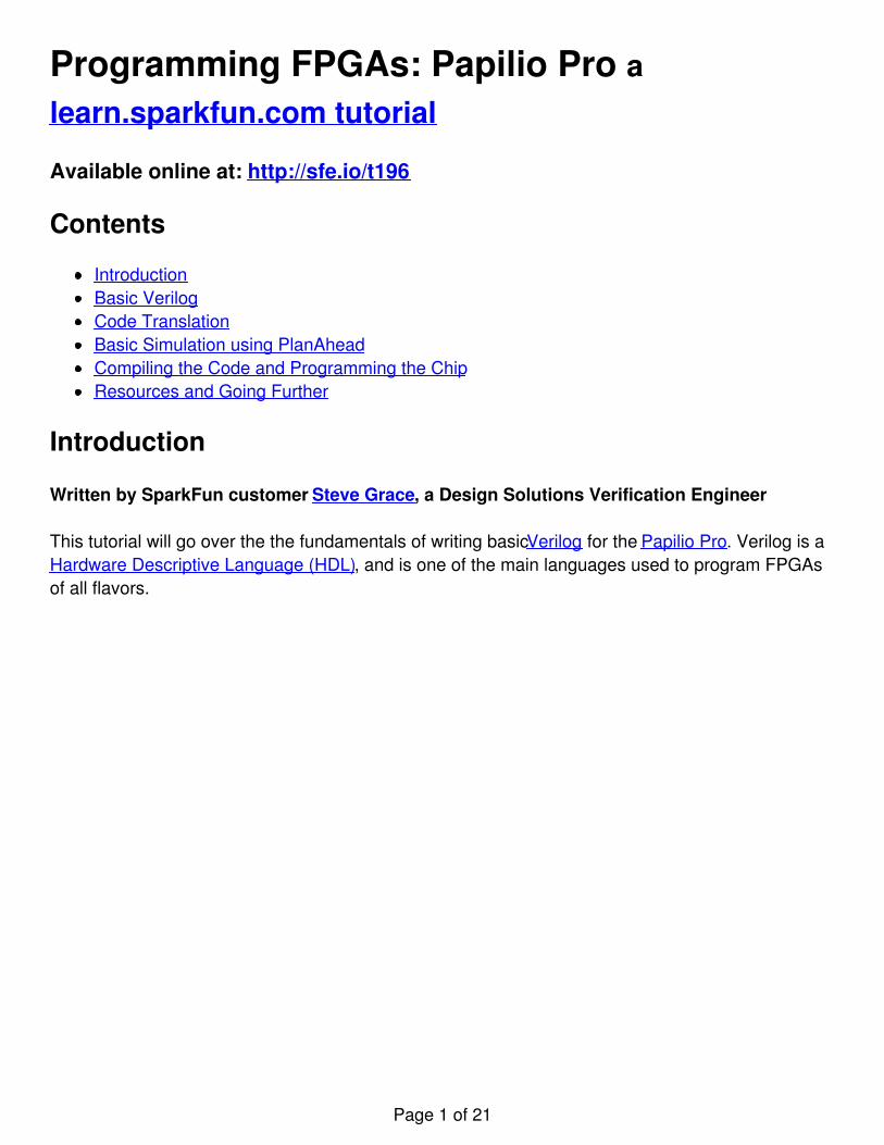
Papilio Pro LX9
DEV-11838RetiredFavorited Favorite 0Wish List
Required Materials
The following items are utilized in this tutorial:
1. Xilinx ISE WebPACK Tools Note: You will want the latest ISE Version (project was madeusing 14.7) ISE Design Suite
2. Papilio Pro3. Sparkfun Cerberus USB Cable4. Papilio Button/LED Wing5. Papilio Program Software6. The Project Source Code from GitHub
Covered in This Tutorial:
Page 2 of 21
Basic Verilog
There are two major HDL styles, Verilog and VHDL. Each have their pros and cons. Since I wastrained on Verilog, this is the style I will use.
Here are some of the topics that will be detailed in each section: creating modules, I/O ports,counters, instantiating submodules, parameter definitions, and other basic items.
Code Translation
To truly understand how HDL works on an FPGA, you will have to understand some basicstranslations from HDL to hardware cells. The hardware that is described will be Look UpTables(LUTs), flip-flops, registers, carry chains (used in arithmetic), and others.
Basic Simulation using PlanAhead
One of the first aspects of designing hardware for an FPGA is to be able to simulate the design tomake sure it works properly and can handle most invalid inputs without causing glitches or otherodd behavior.
Topics covered in this section will include types of stimulus, how to execute the code, andreading/understanding waveforms.
Compiling the Code and Programming the Chip
You will learn how to generate the bitstream (the file used to program the FPGA) and the use thePapilio Loader to program the SPI Flash or the FPGA itself.
Suggested Reading
This tutorial is fairly advanced (conceptually and programmatically). Please read up on any of thebelow concepts that you are not familoar with before continuing:
Digital LogicBoolean AlgebraLogic LevelsBinary and HexadecimalProgramming basics (due to Verilog being used, C/C++ background/knowledge is highlysuggested due to the similarities of syntax)
Basic Verilog
This section will go over the basic syntax for Verilog and the basic elements. This is a subset of allthe capabilities of Verilog, and I highly recommend reading more into it to understand the power ithas. Comparisons will be made between the C/C++ syntax and Verilog.
Page 3 of 21
Note: the code provided in this section is not in the example project. This code is to just show thebasics.
Module Definition
In the C++ world, a function is defined as follows:
void function_name(data_type param1, data_type param2) { // Code Goes Here}
In Verilog, this is how a module is defined:
module module_name( input clk, input rst, input [7:0] data_in, output [7:0] data_out);
// Module code goes here
endmodule
As you can see, there are clear differences and similarities. For starters, the input and output are theI/O ports of this module. You can define as many as you want. For buses, you use the [#:#], the [7:0]
in this case, and adjust how big it is.
Like C++ functions, modules can be called within other modules. The main function of a C/C++program is a function, so a Verilog module can be the “main” function of the design. This “main”function is referred to as the “top level” of the design. Top levels follow the behavior of top-downdesign, bottom-up implementation.
Top-down design is the process of taking your design and breaking it up into smaller components,allowing you to then reuse them. It’s the same as writing C/C++ functions to do specific tasks.
I/O Ports
As shown in the previous segment, this list contains the types of I/O ports: input, output, inout. Theseare like data types in C/C++ and help define the flow of data in the module.
Each is unique, especially inout, but generally, you will only use input and output.
In the module defined above, we have 3 input ports and 1 output port. The input has a bus size of 8(remember, in electronics and programming, we count from 0). The output has the same size bus.
Now that we have a good framework to begin writing a module, let’s build a simple synchronouscounter.
CountersPage 4 of 21

A counter, as you can guess, is something that counts. There are different ways to count, eachhaving their own benefits. The different types of counters are:
Binary-coded Decimal (BCD) CounterBinary Up/Down CounterHex/Oct Counter
This list is not complete, because people can write their own counters to do what they want. For us,we’ll do a typical binary up/down counter.
To understand counters, here’s a typical C++ version we’ll convert to Verilog.
for(int i = 0; i < MAX; i++) { if( count_up == 1) counter += 1; else if ( count_up == 0 && counter != 0) counter -= 1;}
First and foremost, let’s break down what it is doing so we can apply this knowledge later.
1. We are initializing the for-loop’s parameters to start at 0 and go to MAX. We don’t know whatMAX is, but we will not count higher than that. And, we’ll only increment by 1.
2. We are checking to see if the variable count_up is set to 1. If so, we increment the count up,otherwise, we will count down.
3. If we count down, we need to make sure counter is not 0. The reason is because 0 is thelowest we can count.
Now, let’s look at the equivalent code for Verilog.
module counter_mod( input clk, input rst, input count_up, output reg [MAX-1:0] counter);
parameter MAX = 8;
always @(posedge clk) begin if(rst) counter <= 0; else begin if(count_up == 1) counter <= counter + 1; else if(count_up == 0 && counter != 0) counter <= counter - 1; else counter <= 0; endend
endmodule
Page 5 of 21
The module name is counter_mod, and it has 3 input and 1 output ports. Don’t worry about some of theuniqueness of the I/O Ports (they can get complicated, I recommend Googling if you havequestions).
We also have a parameter, which will be discussed later.
Finally, we have the meat of the module, the actual counter. One key concept a lot of people fail tounderstand about HDL is that the code executes in parallel, but is written sequentially.
Let’s break down the code:
1. The always is a term that means, “Always do this block of code every time the clk inputchanges on a positive edge.”
2. To make sure we are synchronous, we need to handle a reset signal, and that is where theif(rst) comes in.
3. Blocks of code don’t use { or } for denoting the end of the function. Rather, in Verilog, it’s thebegin and end. Verilog is similar to C/C++ in that assumes the first line after a command isnested inside that command.
4. Now the actual code of counting. Notice how it’s extremely similar to the C++ version?
You might be asking yourself, “What is with that extra else statement?” The answer is latches. Insynchronous designs, we can sometimes write code that might accidentally create memoryelements called latches. These latches aren’t bad, but they’re not expected (they are really glitchesin the system). In order to not have a glitch, we need to put the counter at a reset state.
Submodule Instantiation
As stated earlier, modules can be called, or instantiated, in other modules like functions withinfunctions in C++, and it follows the same basic idea.
In C++:
void function_1( data_type param1, data_type param2) { // Code Goes Here}
void function_2( data_type param1, data_type param2) { // Code Goes Here}
void function_3( data_type param1, data_type param2) { function_1(param1, param2); function_2(param1, param2);}
Since the counter we wrote could be considered a top-level module, I want to make a coupleinstantiations. To do this:
module top ( input clk,
Page 6 of 21
input rst, input [1:0] count_up, output [MAX-1:0] counter1, output [MAX-1:0] counter2);
parameter MAX = 8;
// First countercounter_mod #( .MAX(MAX)) counter1 ( .clk(clk), .rst(rst), .count_up(count_up[0]), .counter(counter1));
// Second countercounter_mod #( .MAX(MAX)) counter2 ( .clk(clk), .rst(rst), .count_up(count_up[1]), .counter(counter2));
endmodule
Let’s break down the code we just added.
1. Like in C++, we use the module name to start off, but the first parenthesis defines moduleparameters (again explained later). Then comes the I/O. In C/C++, the position of theparameter defines what variable it’s tied to, and Verilog can do it this way, but it’s not theproper way to do so. For Verilog, we use the name of the instantiation model I/O port (eg. clk
with a signal tied to it). This allows us to build complex hierarchy.2. Remember the buses? Well, instead of writing out individual ports for count_up, I created a bus,
which allows me to reuse the name but select the individual signal (count_up[0] and count_up[1]).3. Now, this code implements 2 independent counters, with counter1 and counter2. We can do a tri-
state, and have it alternate between the two, but for this tutorial, this is enough.
Parameters of Modules
The concept of a parameter is the equivalent to a const variable in C/C++. A const variable is avariable in C++ that takes up memory but can never be altered by the program.
C++ syntax:
const int MAX = 8;
Verilog:
Page 7 of 21
parameter MAX = 8;
As with the const, parameter cannot have the value adjusted on the fly during compilation. Unlike acomputer program, FPGAs cannot handle dynamic memory allocation, so everything must bedefined.
Note: Verilog has macro capability which is sometimes used in place of parameters. As anexample:
`define MAX 8
module ( ... input [`MAX-1:0] data_in, ...);
...
endmodule
However, unlike the macros in C/C++, a ` mark has to be used to denote if it’s a macro or not.
Generally, people use macros to simplify segments of Verilog to be more readable.
Synchronous/Asynchronous Logic
This section will go into detail on the synchronous/asynchronous logic with respect to FPGAs.
Generally, digital logic designers follow this advice: K.I.S.S. = Keep It Synchronous, Stupid.
What are the advantages and disadvantages for the two?
Synchronous
Advantages:
1. Safe states, so if a glitch occurs, it goes to a state in which the system can recover easily.2. Allows for better optimization on designs.3. Resets are forced to follow clock cycles.
Disadvantages:
1. Multi-clock designs will have multiple resets, which might not be tied together2. Requires a clock at all times.3. Potential higher use of tri-state buffering
Asynchronous
Advantages:
Page 8 of 21
1. Faster capabilities with data (data will generally be more correct)2. Removal of reset from the data path (path in which data follows the clock)3. Multi-clock designs only need 1 system reset
Disadvantages:
1. Simulations might not work appropriately2. Has to be generated from I/O, never internally.3. De-asserting a reset signal can cause problems.
Which option is best for you? The best answer if you are just getting started with FPGAs is to runsynchronously. Remember, K.I.S.S.
The reason for keeping things synchronous is because of the inherit inability to know what thesystem does if there is no “safe state.” Let’s look at the counter code with an asynchronous reset.
always @(posedge clk or negedge rst) begin if(!rst) counter <= 0; else begin if(count_up == 1) counter <= counter + 1; else if(count_up == 0 && counter != 0) counter <= counter - 1; else counter <= 0; endend
If this system were to hit the reset signal, once the de-assertion of it occurs (goes from positive tonegative; hence the negedge), the system stops what it is doing and immediately sets counter to allzeroes. Now the propagation delay (time it takes for data to travel from the input to the output), willbe different for every element on the FPGA. On a big design, it could take nanoseconds to finishde-asserting the reset, and, by then, data could potentially get corrupted or glitches may occur.
Timing plays a very large role in FPGA design. Timing is the idea that your design will make suredata gets to where it needs to go in the appropriate time.
Code Translation
This section will cover how parts of code learned in the previous section are translated to thehardware of the FPGA. Remember, FPGAs have a finite amount of space for you to create yourdesign. Knowing how code translates to the hardware will help plan for optimization techniques andwhere to place it on the chip’s floor.
I’ll take the clock divider provided in the Github example to explain how it translates to thehardware. Knowing how to translate from code to hardware helps you understand what is reallygoing on. Instead of blindly assuming the compiler is doing things right (similar to compiling a C++program), we will make sure it is translated the way we want/need it to be.
Page 9 of 21
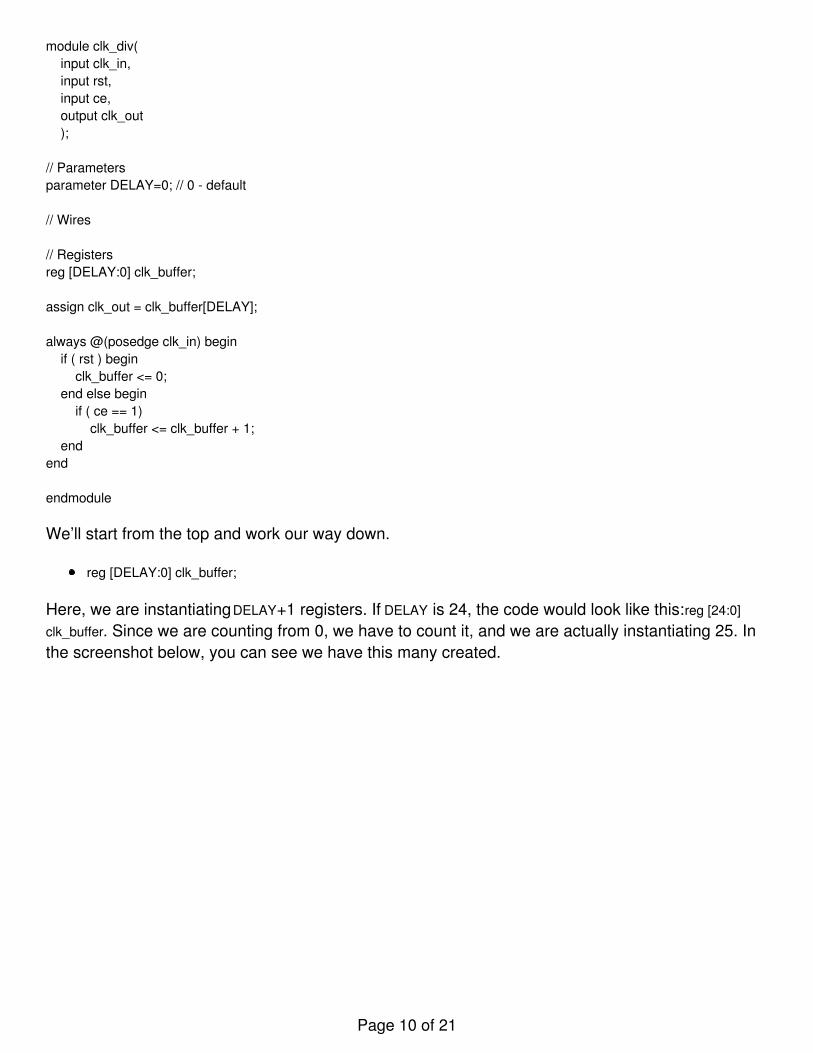
module clk_div( input clk_in, input rst, input ce, output clk_out );
// Parametersparameter DELAY=0; // 0 - default
// Wires
// Registersreg [DELAY:0] clk_buffer;
assign clk_out = clk_buffer[DELAY];
always @(posedge clk_in) begin if ( rst ) begin clk_buffer <= 0; end else begin if ( ce == 1) clk_buffer <= clk_buffer + 1; endend
endmodule
We’ll start from the top and work our way down.
reg [DELAY:0] clk_buffer;
Here, we are instantiating DELAY+1 registers. If DELAY is 24, the code would look like this: reg [24:0]
clk_buffer. Since we are counting from 0, we have to count it, and we are actually instantiating 25. Inthe screenshot below, you can see we have this many created.
Page 10 of 21
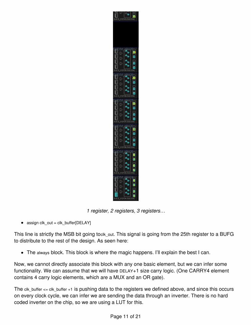
1 register, 2 registers, 3 registers…
assign clk_out = clk_buffer[DELAY]
This line is strictly the MSB bit going to clk_out. This signal is going from the 25th register to a BUFGto distribute to the rest of the design. As seen here:
The always block. This block is where the magic happens. I’ll explain the best I can.
Now, we cannot directly associate this block with any one basic element, but we can infer somefunctionality. We can assume that we will have DELAY+1 size carry logic. (One CARRY4 elementcontains 4 carry logic elements, which are a MUX and an OR gate).
The clk_buffer <= clk_buffer +1 is pushing data to the registers we defined above, and since this occurson every clock cycle, we can infer we are sending the data through an inverter. There is no hardcoded inverter on the chip, so we are using a LUT for this.
Page 11 of 21
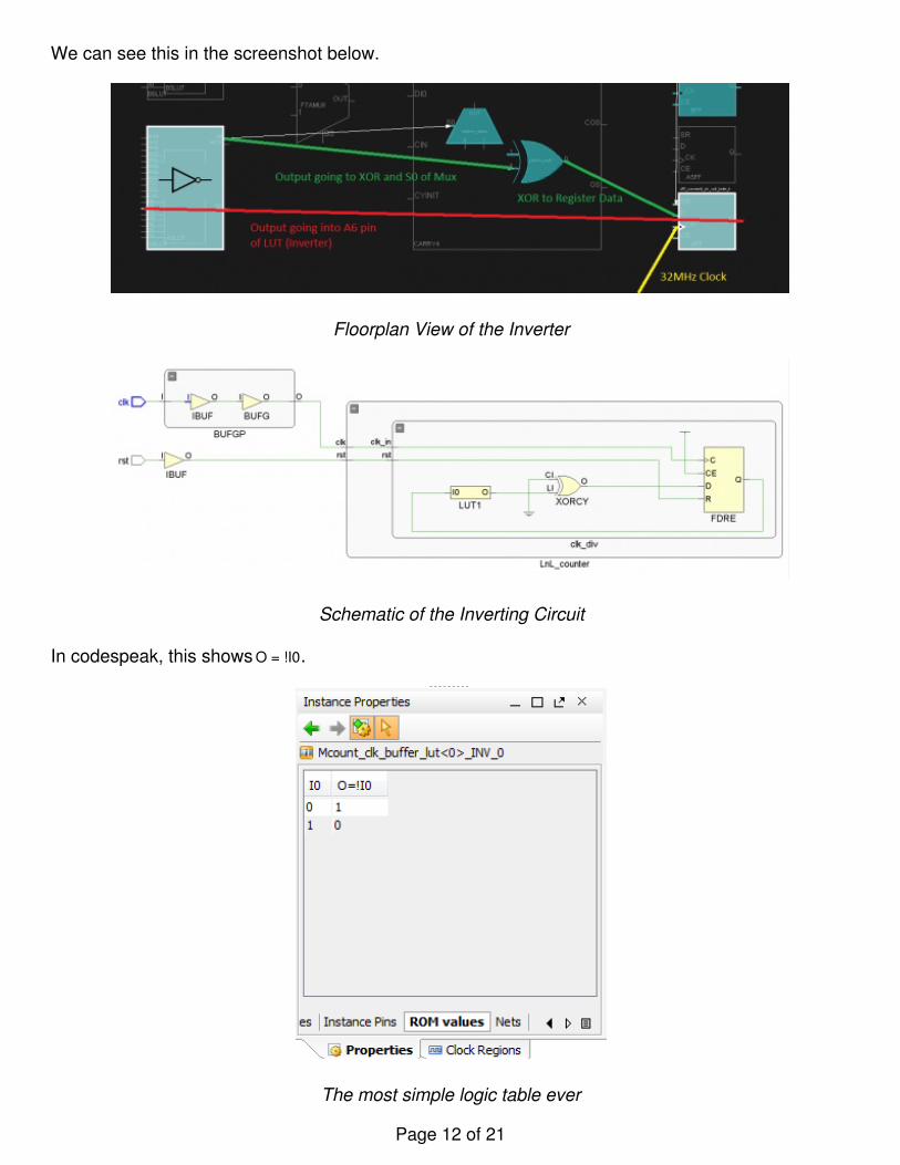
We can see this in the screenshot below.
Floorplan View of the Inverter
Schematic of the Inverting Circuit
In codespeak, this shows O = !I0.
The most simple logic table ever
Page 12 of 21

In laymen terms, this means the input 0 of the LUT will be inverted to the output.
Where is the LUT input coming from? The answer is clk_buffer[0]. This is confusing, because we areactually using the main system clock to drive these registers (posedge clk_in).
On reset (power up) the 25 registers set their initial inputs to 0. From here the clk_in starts to run.After the first clock cycle (positive edge to positive edge), clock_buffer[0] sends its value, which is a 0,to the LUT, which inverts it and sends it to the first carry logic MUX and OR. The OR sends it toclk_buffer[1] and the MUX as a select signal to the next carry logic. It does this 24 more times, and weget to clk_buffer[24]. There, the output goes to a BUFG element where it gets distributed to the rest ofthe design.
This code will run like this until power is lost.
I invite you to do the same sort of translation for the other modules and see how well you do.
Basic Simulation using PlanAhead
Now that we know the basics of HDL, let’s get into the project of this tutorial.
A few notes on the project:
The project itself DOES NOT MEET TIMING. This is due to the clock domain conversionbeing performed within the program.The project already contains an existing bitstream.I tried to comment as much as possible, while keeping it from being a novel. If you have anyquestions, please post in the comments section.
Simulation is a key part of the FPGA design process. Unlike microcontroller development, we wantto make sure the code we have written functions the way we want it to before pushing it to the chip.Some microcontroller development software provide their own simulation, but in the open sourcearena, I have not seen this.
So why MUST we simulate before we go further?
1. Compilation takes time and a lot of resources (depending on the design). It is not wise to gothrough this flow for every little change in the design.
2. FPGAs by definition are not cheap parts (unless you buy in bulk). An incorrect design doeshave a slim chance on damaging the board, chip, or both.
3. We can find bugs in the code earlier and fix them without even compiling the code, whichmakes things faster.
These are my top three answers. Others might agree/disagree, but that is the beauty ofengineering.
How to Run the Code
Page 13 of 21

Once you have installed the program files, open up PlanAhead, and select “Create New Project”.Choose the path where you would like your project to be located. You can then navigate to thesource files you downloaded previously. Choose the “Spartan 6” as the Family and the“XC6SLX9tqg144-2” as the Project Part.
How to Stimulate the Code
Writing stimulus for simulation is fairly easy and by far one of the more creative aspects of FPGAdesigns. The reason is, you get to find ways to break the design in the fewest lines of code.
Here is the stimulus for the clock divider (clk_div_tb.v) in the previous sections:
`timescale 1ns / 1ps
module clk_div_tb();
reg clk_in;reg rst;reg ce;
wire [nDelay-1:0] clk_out;
parameter nDelay = 32;
genvar i;generate for(i = 0; i < nDelay; i = i + 1) begin clk_div #( .DELAY(i) ) DUT ( .clk_in(clk_in), .rst(rst), .ce(ce), .clk_out(clk_out[i]) ); endendgenerate
always #15.625 clk_in = ~clk_in;
// Initial input statesinitial begin clk_in = 0; rst = 1; ce = 1;end
// Test procedure belowinitial begin #100 rst = 0;
end
endmodule
Page 14 of 21
Let’s break down the code.
1. The stimulus (test bench) is considered a module ON TOP of the module in test. In this caseclk_div_tb is the top-level of clk_div.
2. Inputs are always reg and outputs are always wires. The reason is, you manipulate the inputsand it has to process through the system to the outputs. (We will be able to tap into thedesign’s internal wires.)
3. We are generating clock dividers on purpose here. The generate block lets us do multipleinstantiations of the clk_div instance. The genvar is the variable we use in the for-loop to keepthings consistent (think of this as doing an int i for C++ and then using the i as the loopvariable.
The reason we are generating 32 of these is because, at the time I was not sure whichdelay value was going to be the best. By doing it this way, I could easily check whichdelay value would be best.
4. The always block is basically saying, “clk_in is going to be going from logic low/high to high/low(depending on the reset state of clk_in”. The value #15.625 is used because that is matching thefrequency that is used by the Papilio Pro.
5. Next is the initial values. All inputs will have initial values. This is why we always design with areset state in mind. Here, clk_in is logic low, rst and ce are logic high.
6. We add our stimulus in the test procedure block. Here, we see that after #100 we set our rst tologic low. (This means our reset is active high). The #100 dignifies how many time units it’ll befrom the start ‘til rst’s value changes.
If you wanted to add stimulus to this after the reset, you could. As an example, you canput: #150 ce = 0; . This means, after 50 clock pulses, make the ce signal GND, or basicallyturn off this submodule.
See the timescale 1ns/1ps at the top? This tells the simulator the unit value of # and the resolution. Inthis case, 1ns is our unit of time, and 1ps is our resolution. This is extremely detailed for our design,but it works since we are working with a 32MHz clock frequency.
Running the Simulation
In PlanAhead, running a simulation is quite easy.
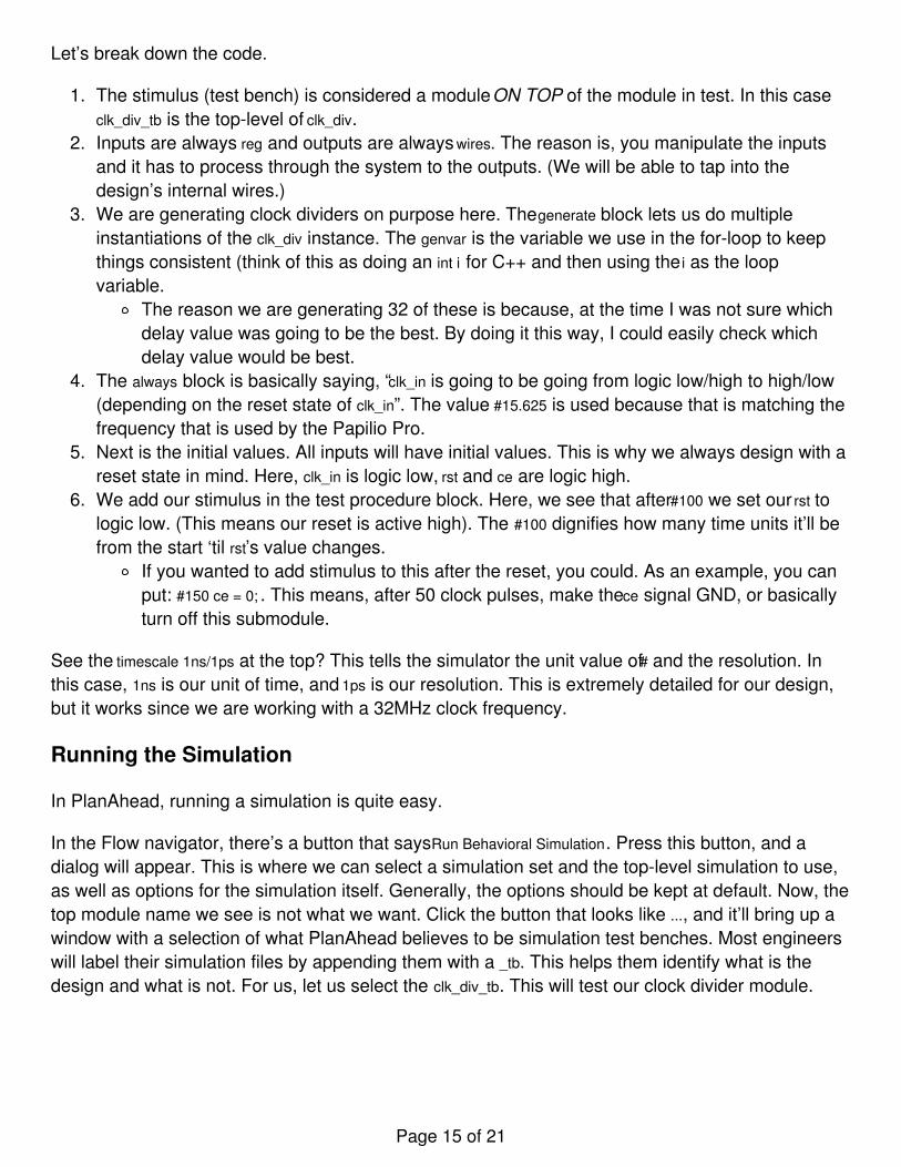
In the Flow navigator, there’s a button that says Run Behavioral Simulation. Press this button, and adialog will appear. This is where we can select a simulation set and the top-level simulation to use,as well as options for the simulation itself. Generally, the options should be kept at default. Now, thetop module name we see is not what we want. Click the button that looks like ..., and it’ll bring up awindow with a selection of what PlanAhead believes to be simulation test benches. Most engineerswill label their simulation files by appending them with a _tb. This helps them identify what is thedesign and what is not. For us, let us select the clk_div_tb. This will test our clock divider module.
Page 15 of 21
Click Launch. This will launch the ISim software provided and run the test. By default, it’ll run for5microseconds, and, for the purpose of this tutorial, that is long enough. Wait for it finish, and thenwe’ll look at the waveforms.
Understanding the Waveforms
Waveforms is a set of signals that we determine to be important enough to warrant us viewing themand analyzing the fine timing of positive and negative edge changes.
NOTE: Simulations use “ideal” switching. This means that they are GND and VCC at the same timein the viewer. In reality, this is not true.
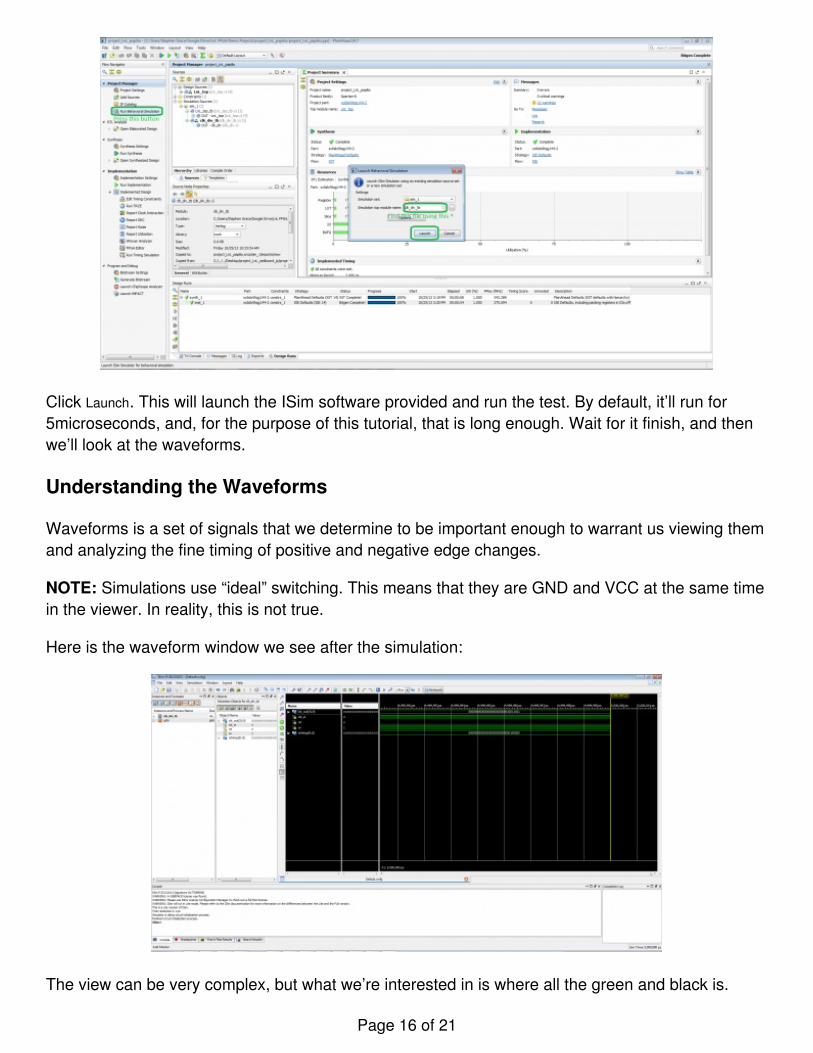
Here is the waveform window we see after the simulation:
The view can be very complex, but what we’re interested in is where all the green and black is.
Page 16 of 21
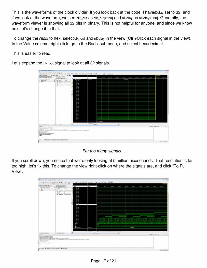
This is the waveforms of the clock divider. If you look back at the code, I have nDelay set to 32, andif we look at the waveform, we see clk_out as clk_out[31:0] and nDelay as nDelay[31:0]. Generally, thewaveform viewer is showing all 32 bits in binary. This is not helpful for anyone, and since we knowhex, let’s change it to that.
To change the radix to hex, select clk_out and nDelay in the view (Ctrl+Click each signal in the view).In the Value column, right-click, go to the Radix submenu, and select hexadecimal.
This is easier to read.
Let’s expand the clk_out signal to look at all 32 signals.
Far too many signals…
If you scroll down, you notice that we’re only looking at 5 million picoseconds. That resolution is fartoo high, let’s fix this. To change the view right-click on where the signals are, and click “To FullView”.
Page 17 of 21
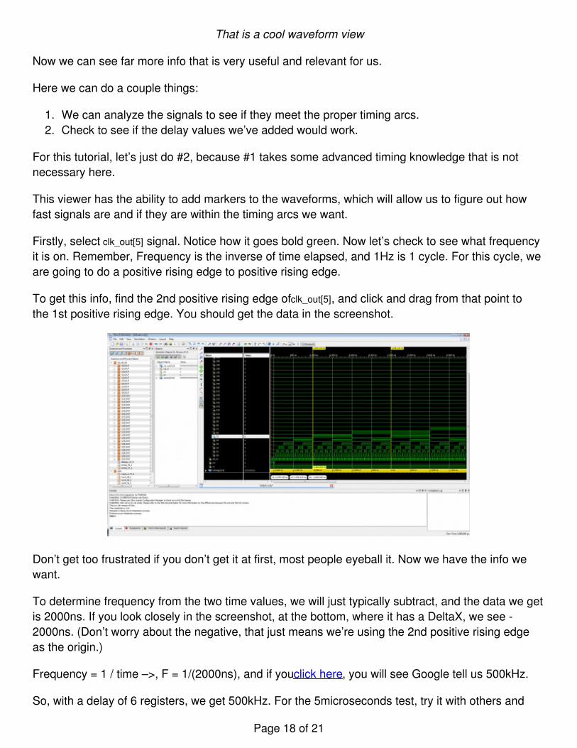
That is a cool waveform view
Now we can see far more info that is very useful and relevant for us.
Here we can do a couple things:
1. We can analyze the signals to see if they meet the proper timing arcs.2. Check to see if the delay values we’ve added would work.
For this tutorial, let’s just do #2, because #1 takes some advanced timing knowledge that is notnecessary here.
This viewer has the ability to add markers to the waveforms, which will allow us to figure out howfast signals are and if they are within the timing arcs we want.
Firstly, select clk_out[5] signal. Notice how it goes bold green. Now let’s check to see what frequencyit is on. Remember, Frequency is the inverse of time elapsed, and 1Hz is 1 cycle. For this cycle, weare going to do a positive rising edge to positive rising edge.
To get this info, find the 2nd positive rising edge of clk_out[5], and click and drag from that point tothe 1st positive rising edge. You should get the data in the screenshot.
Don’t get too frustrated if you don’t get it at first, most people eyeball it. Now we have the info wewant.
To determine frequency from the two time values, we will just typically subtract, and the data we getis 2000ns. If you look closely in the screenshot, at the bottom, where it has a DeltaX, we see -2000ns. (Don’t worry about the negative, that just means we’re using the 2nd positive rising edgeas the origin.)
Frequency = 1 / time –>, F = 1/(2000ns), and if you click here, you will see Google tell us 500kHz.
So, with a delay of 6 registers, we get 500kHz. For the 5microseconds test, try it with others and
Page 18 of 21

see what values you can get.
Did you notice a pattern? For each additional register we add, the delay increases by 2x. Meaning,if you did the clk_out[4] you would see 1000kHz (1MHz).
Pretty slick, huh?
Now let’s make sure the signals, falling edges on clk_out[5], and clk_out[4] are in sync. Go ahead andselect one of the falling edges for clk_out[5], and you will notice that it is in sync with other signals.This is a good thing, because it means things are in working order and timing is met properly. If itwas not meeting timing properly, signals would be skewed, and using the skill we learned above,could determine the difference to figure out if it is meeting timing constraints (setup/hold) or not.
By George, they meet timing!
Now that I’ve shown you some basics, go ahead and close the simulator. It will ask you if you wantto save the .wcfg file. This basically means the next time you run this simulation, it’ll display thewaveforms this way. Go ahead and save it.
To explore a bit further, I suggest modifying the clk_div_tb.v by adding #150 ce = 0; below the #100 rst = 0;
, saving the file, running another simulation, and seeing what happens.
From here on, it only gets more advanced, and I recommend watching videos, and reading articleson ISim to understand it better.
Compiling the Code and Programming the Chip
Once all the code is written, syntactically correct, and compiles all the way through Implementation,it is time to generate the bitstream and program the Papilio Pro.
Luckily, the compiling the code is the easiest part of the whole tutorial. Assuming the code is right,you can just click the “Generate Bitstream” button in the Flow Navigator, and it will run through all
Page 19 of 21
the steps of the tool (Synthesis and Implementation) and generate the .bit file. If code is wrong inanyway, it will stop at the last known good state, throw error messages, which you will need to useto investigate and fix the code.
If all is well you will have a .bit file ready to go!
To program the Papilio Pro, we need the Papilio Loader to know where the .bit file is. ForPlanAhead, where you saved your project, there is a <project_name>.runs/impl_1 (LnL_top.bit) directory.This directly contains the .bit file. It should have the same name as the top level module.
Copy this path, and open up the Papilio Loader (make sure the Papilio Pro is plugged into thecomputer). Leave everything in the default settings. We want to limit any potential JTAG issues.Click the “browse” button next to the Bistream text box, and paste the path. The bitstream fileshould appear.
Note: The Papilio Pro Loader will remember the last path used, so if you use the same project, youdon’t need to change anything in the loader.
Now that everything is good to go, click the program button! The textbox in the window will spewsome diagnostic items, and it should tell you if it was successful.
Once this is done, go ahead and press the buttons!
Congratulations, you just programmed your first FPGA from a design!
Resources and Going Further
I urge you to continue to learn about FPGAs by searching the web and reading as much as possibleon it. FPGAs are not the easiest thing to learn, but provide quite a bit of power and functionality thatis always cool to do. Understanding the power of FPGAs will take a fair bit of time and energy. Theyare extremely complex, extremely powerful, and most of the things you utilize today (mainly theInternet) run on these amazing little chips.
The best advice I can give out to learning FPGAs is to find a project that will utilize one, and do it.
A few suggested places to visit to get a better understanding are:
Asic-World - Great place to learn HDL, Scripting, and a variety of items on FPGAs and digitallogicFPGA4Fun - A site for non-novices, but provides great tutorials on projects and IP as well asgeneral FPGA information.Hamster Works - A novice-turned-expert in the field of FPGAs and embedded electronics. Hewrote an FPGA book for novices! He also provides great insight into projects and tutorials.Any and all digital logic textbooks. They are undervalued in this world, so if you can pick upone or two, keep them forever. They are worth their weight in gold.
learn.sparkfun.com | CC BY-SA 3.0 | SparkFun Electronics | Niwot, ColoradoPage 20 of 21

Page 21 of 21