Embed Size (px)
Citation preview

1
Programmable
Peripheral Interface
(PPI) – 8255A
CEN433
King Saud University
Dr. Mohammed Amer Arafah
Mohammed Amer Arafah2CEN433 - King Saud University
Functional Diagram
Mohammed Amer Arafah3CEN433 - King Saud University
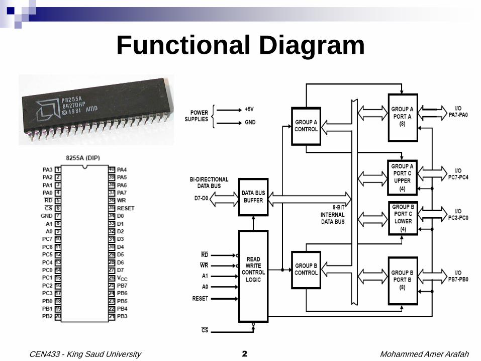
Pin Description
Mohammed Amer Arafah4CEN433 - King Saud University
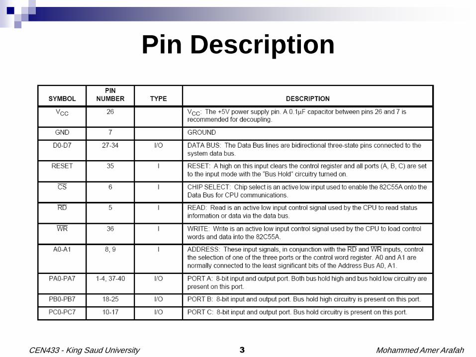
8255A Basic Operation
A1 A0 Port
0 0 Port A
0 1 Port B
1 0 Port C
1 1 Control Word
Mohammed Amer Arafah5CEN433 - King Saud University
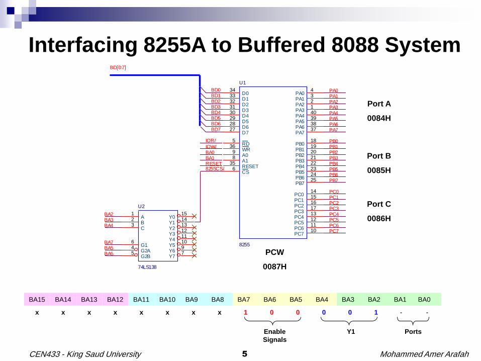
Interfacing 8255A to Buffered 8088 System
BD0BD1BD2BD3BD4BD5BD6BD7
PA0PA1PA2PA3PA4PA5PA6PA7
PB0PB1PB2PB3PB4PB5PB6PB7
PC0PC1PC2PC3PC4PC5PC6PC7
IOR/
IOW/BA0BA1RESET
BD[0:7]
8255CS/
BA2BA3BA4
BA5BA6
BA7
U1
8255
D034
D133
D232
D331
D430
D529
D628
D727
RD5
WR36
A09
A18
RESET35
CS6
PA04
PA13
PA22
PA31
PA440
PA539
PA638
PA737
PB018
PB119
PB220
PB321
PB422
PB523
PB624
PB725
PC014
PC115
PC216
PC317
PC413
PC512
PC611
PC710
U2
74LS138
A1
B2
C3
G16
G2A4
G2B5
Y015
Y114
Y213
Y312
Y411
Y510
Y69
Y77
BA15 BA14 BA13 BA12 BA11 BA10 BA9 BA8 BA7 BA6 BA5 BA4 BA3 BA2 BA1 BA0
x x x x x x x x 1 0 0 0 0 1 - -
Port A
0084H
Port B
0085H
Port C
0086H
PCW
0087H
Y1Enable
Signals
Ports
Mohammed Amer Arafah6CEN433 - King Saud University
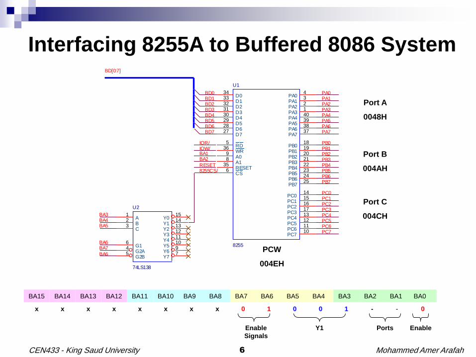
Interfacing 8255A to Buffered 8086 System
BA15 BA14 BA13 BA12 BA11 BA10 BA9 BA8 BA7 BA6 BA5 BA4 BA3 BA2 BA1 BA0
x x x x x x x x 0 1 0 0 1 - - 0
Port A
0048H
Port B
004AH
Port C
004CH
PCW
004EH
Y1Enable
Signals
Ports
PB2
BD2
BA1BA2
BD6
IOR/
PB5
PB3
PA5
BA6
BA7
8255CS/
PB1PB0
BD4
PB4
PB6
PA2
PA0
PB7
BD1
BA4
IOW/
PA7
PC0
PC6
PA4
BD[0:7]
BA6
BA5PC5
PA6
BD0
PC4
BD5
BD3
PC3
PC1
PA1
BD7
PC2
PC7
BA3
RESET
PA3
U2
74LS138
A1
B2
C3
G16
G2A4
G2B5
Y015
Y114
Y213
Y312
Y411
Y510
Y69
Y77
U1
8255
D034
D133
D232
D331
D430
D529
D628
D727
RD5
WR36
A09
A18
RESET35
CS6
PA04
PA13
PA22
PA31
PA440
PA539
PA638
PA737
PB018
PB119
PB220
PB321
PB422
PB523
PB624
PB725
PC014
PC115
PC216
PC317
PC413
PC512
PC611
PC710
Enable
Mohammed Amer Arafah7CEN433 - King Saud University
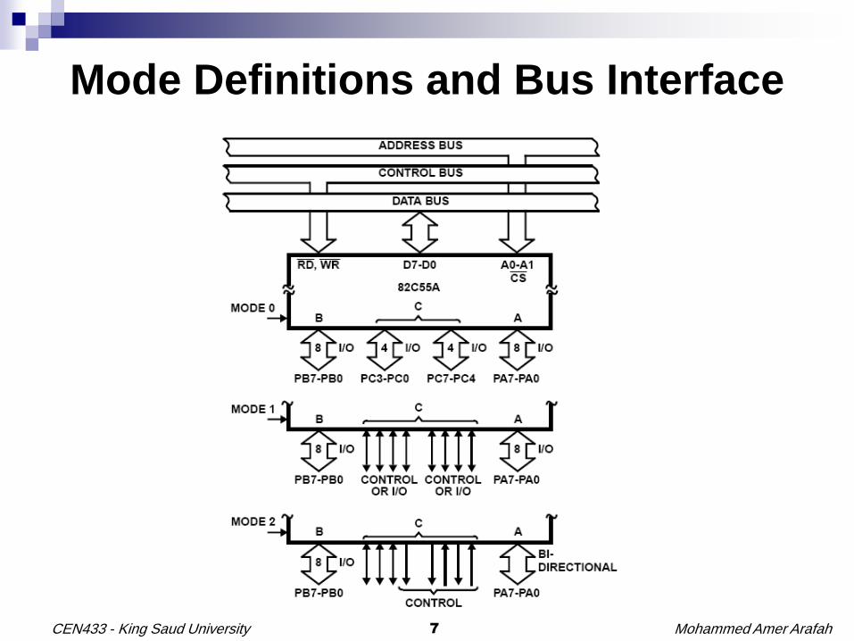
Mode Definitions and Bus Interface
Mohammed Amer Arafah8CEN433 - King Saud University
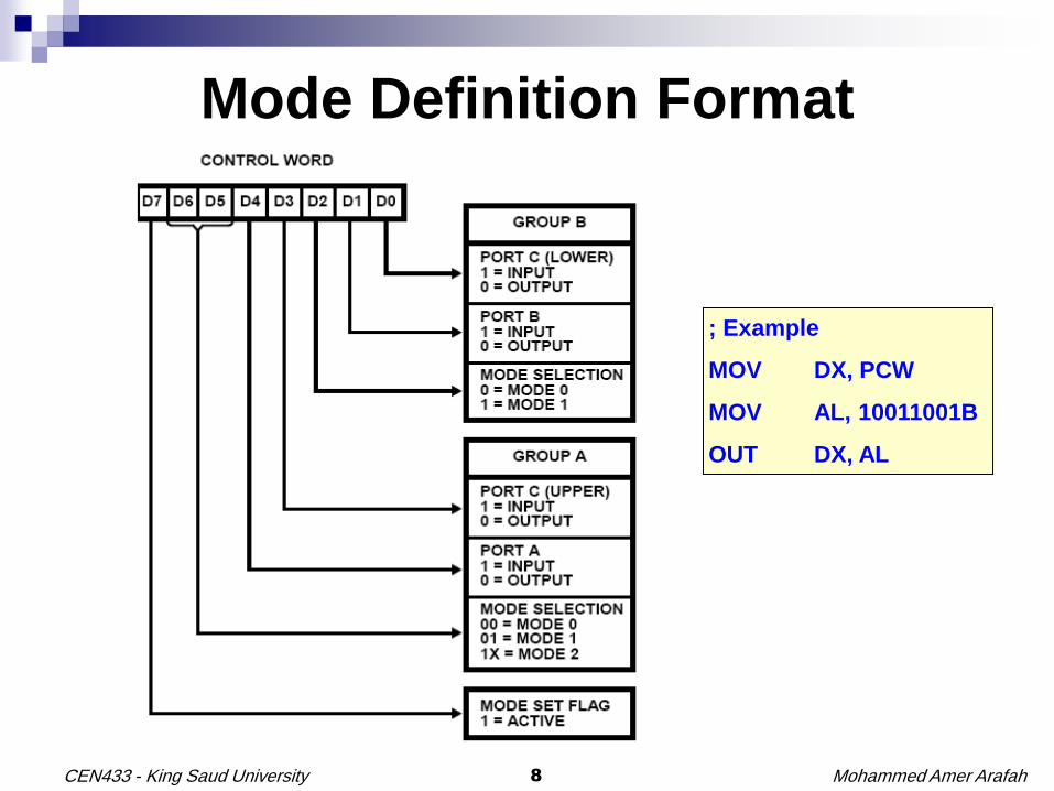
Mode Definition Format
; Example
MOV DX, PCW
MOV AL, 10011001B
OUT DX, AL
Mohammed Amer Arafah9CEN433 - King Saud University
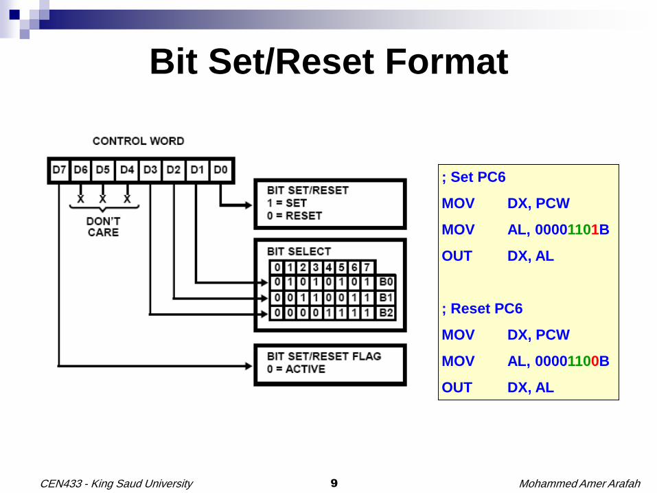
Bit Set/Reset Format
; Set PC6
MOV DX, PCW
MOV AL, 00001101B
OUT DX, AL
; Reset PC6
MOV DX, PCW
MOV AL, 00001100B
OUT DX, AL
Mohammed Amer Arafah10CEN433 - King Saud University
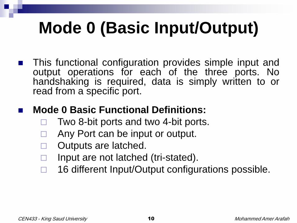
Mode 0 (Basic Input/Output)
This functional configuration provides simple input andoutput operations for each of the three ports. Nohandshaking is required, data is simply written to orread from a specific port.
Mode 0 Basic Functional Definitions:
Two 8-bit ports and two 4-bit ports.
Any Port can be input or output.
Outputs are latched.
Input are not latched (tri-stated).
16 different Input/Output configurations possible.
Mohammed Amer Arafah11CEN433 - King Saud University
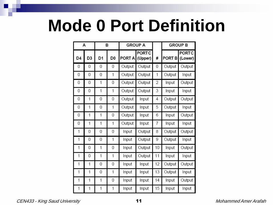
Mode 0 Port Definition
Mohammed Amer Arafah12CEN433 - King Saud University
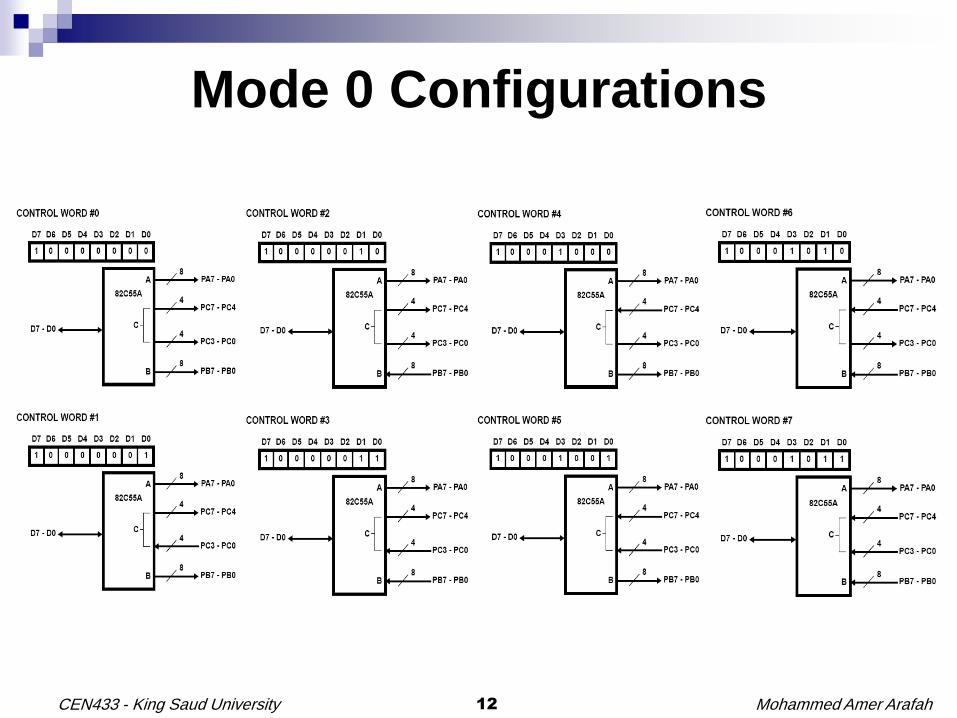
Mode 0 Configurations
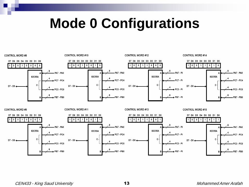
Mohammed Amer Arafah13CEN433 - King Saud University
Mode 0 Configurations
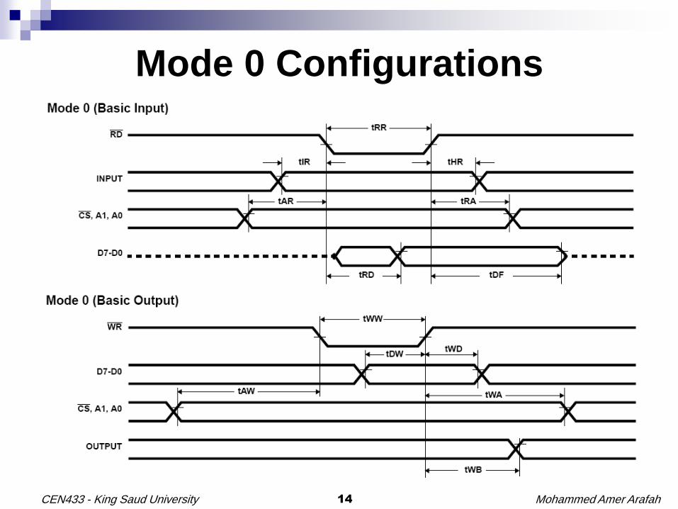
Mohammed Amer Arafah14CEN433 - King Saud University
Mode 0 Configurations
Mohammed Amer Arafah15CEN433 - King Saud University
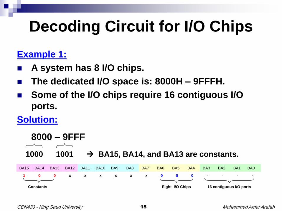
Decoding Circuit for I/O Chips
Example 1:
A system has 8 I/O chips.
The dedicated I/O space is: 8000H – 9FFFH.
Some of the I/O chips require 16 contiguous I/O
ports.
Solution:
8000 – 9FFF
1000 1001 BA15, BA14, and BA13 are constants.
BA15 BA14 BA13 BA12 BA11 BA10 BA9 BA8 BA7 BA6 BA5 BA4 BA3 BA2 BA1 BA0
1 0 0 x x x x x x 0 0 0 - - - -
Eight I/O ChipsConstants 16 contiguous I/O ports
Mohammed Amer Arafah16CEN433 - King Saud University
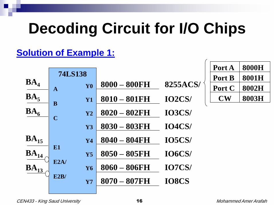
Decoding Circuit for I/O Chips
Solution of Example 1:
8000 – 800FH 8255ACS/
8010 – 801FH IO2CS/
8020 – 802FH IO3CS/
8030 – 803FH IO4CS/
8040 – 804FH IO5CS/
8050 – 805FH IO6CS/
8060 – 806FH IO7CS/
8070 – 807FH IO8CS
74LS138
Y0
Y1
Y2
Y3
Y4
Y5
Y6
Y7
A
B
C
E1
E2A/
E2B/
BA4
BA5
BA6
BA15
BA14
BA13
Port A 8000H
Port B 8001H
Port C 8002H
CW 8003H
Mohammed Amer Arafah17CEN433 - King Saud University
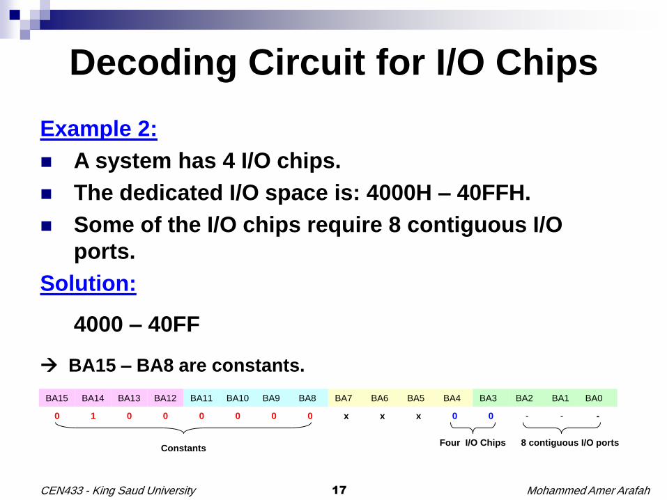
Decoding Circuit for I/O Chips
Example 2:
A system has 4 I/O chips.
The dedicated I/O space is: 4000H – 40FFH.
Some of the I/O chips require 8 contiguous I/O
ports.
Solution:
4000 – 40FF
BA15 – BA8 are constants.
BA15 BA14 BA13 BA12 BA11 BA10 BA9 BA8 BA7 BA6 BA5 BA4 BA3 BA2 BA1 BA0
0 1 0 0 0 0 0 0 x x x 0 0 - - -
Four I/O ChipsConstants
8 contiguous I/O ports
Mohammed Amer Arafah18CEN433 - King Saud University
Decoding Circuit for I/O Chips
Solution of Example 2:
4000 – 4007H 8255ACS/
4008 – 400FH IO2CS/
4010 – 4017H IO3CS/
4018 – 401FH IO4CS/
74LS139
Y0
Y1
Y2
Y3
A
B
E/
BA3
BA4
BA15
BA14
BA13
BA12
BA11
BA10
BA9
BA8
Port A 4000H
Port B 4001H
Port C 4002H
CW 4003H
Mohammed Amer Arafah19CEN433 - King Saud University
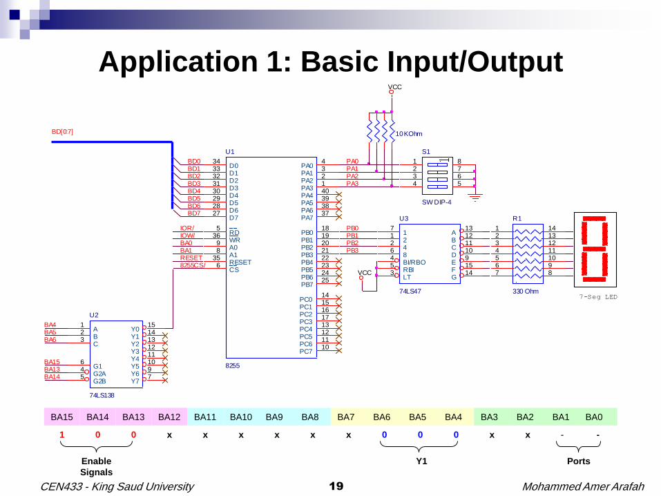
Application 1: Basic Input/Output
7-Seg LED
VCC
VCC
IOR/
BA0BA1
IOW/
BA4
BD3
BD0
RESET
BD6BD5
BD[0:7]
BD2
BA5
BA15
BA6
BD4
BA14BA13
BD7
BD1
8255CS/
PB1
PB3PB2
PB0
PA0PA1PA2PA3
U2
74LS138
A1
B2
C3
G16
G2A4
G2B5
Y015
Y114
Y213
Y312
Y411
Y510
Y69
Y77
R1
330 Ohm
1 142 133 124 115 106 97 8
U3
74LS47
17
21
42
86
BI/RBO4
RBI5
LT3
A13
B12
C11
D10
E9
F15
G14
10 KOhm
U1
8255
D034
D133
D232
D331
D430
D529
D628
D727
RD5
WR36
A09
A18
RESET35
CS6
PA04
PA13
PA22
PA31
PA440
PA539
PA638
PA737
PB018
PB119
PB220
PB321
PB422
PB523
PB624
PB725
PC014
PC115
PC216
PC317
PC413
PC512
PC611
PC710
S1
SW DIP-4
1234
8765
BA15 BA14 BA13 BA12 BA11 BA10 BA9 BA8 BA7 BA6 BA5 BA4 BA3 BA2 BA1 BA0
1 0 0 x x x x x x 0 0 0 x x - -
Y1Enable
Signals
Ports
Mohammed Amer Arafah20CEN433 - King Saud University
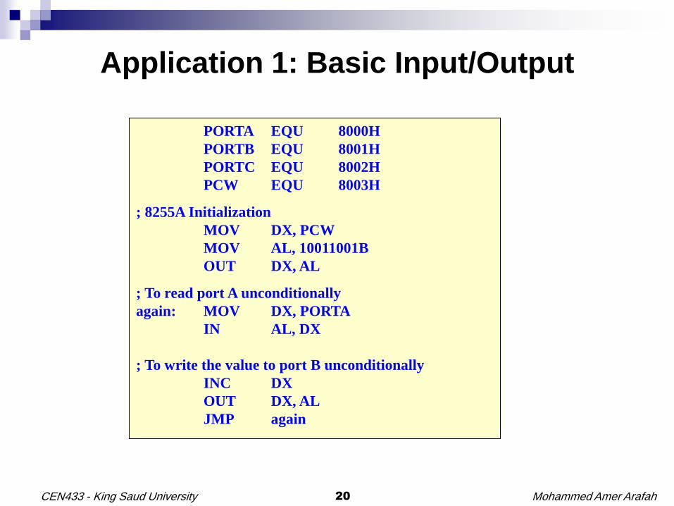
Application 1: Basic Input/Output
PORTA EQU 8000H
PORTB EQU 8001H
PORTC EQU 8002H
PCW EQU 8003H
; 8255A Initialization
MOV DX, PCW
MOV AL, 10011001B
OUT DX, AL
; To read port A unconditionally
again: MOV DX, PORTA
IN AL, DX
; To write the value to port B unconditionally
INC DX
OUT DX, AL
JMP again
Mohammed Amer Arafah21CEN433 - King Saud University
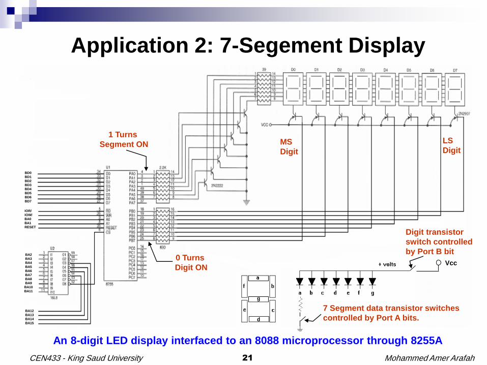
BD0
BD1
BD2
BD3
BD4
BD5
BD6
BD7
IOR/
IOW/
BA0
BA1
RESET
BA2
BA3
BA4
BA5
BA6
BA7
BA8
BA9
BA10
BA11
BA12
BA13
BA14
BA15
MS
Digit
LS
Digit
1 Turns
Segment ON
0 Turns
Digit ON
Application 2: 7-Segement Display
An 8-digit LED display interfaced to an 8088 microprocessor through 8255A
Digit transistor
switch controlled
by Port B bit
7 Segment data transistor switches
controlled by Port A bits.
Vcc
Mohammed Amer Arafah22CEN433 - King Saud University
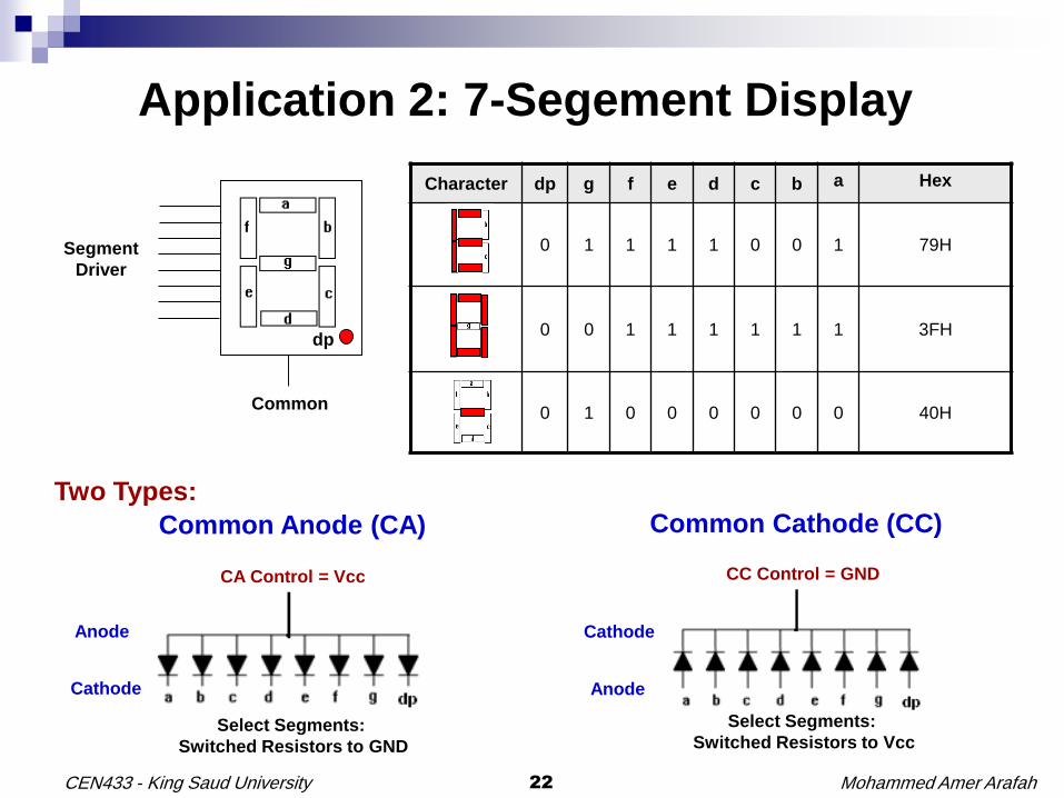
Application 2: 7-Segement Display
dp
Common
Segment
Driver
Two Types:
Cathode
Anode
CA Control = Vcc
Select Segments:
Switched Resistors to GND
Common Anode (CA)
Cathode
Anode
CC Control = GND
Common Cathode (CC)
Select Segments:
Switched Resistors to Vcc
Character dp g f e d c b a Hex
0 1 1 1 1 0 0 1 79H
0 0 1 1 1 1 1 1 3FH
0 1 0 0 0 0 0 0 40H
Mohammed Amer Arafah23CEN433 - King Saud University
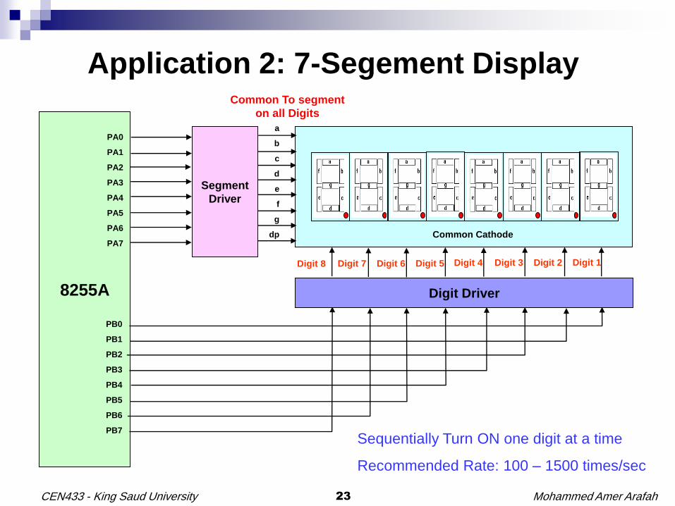
Application 2: 7-Segement Display
8255A
Segment
Driver
PA0
PA1
PA2
PA3
PA4
PA5
PA6
PA7
PB0
PB1
PB2
PB3
PB4
PB5
PB6
PB7
a
b
c
d
e
f
g
dp
Digit Driver
Common To segment
on all Digits
Digit 8 Digit 7 Digit 6 Digit 5 Digit 4 Digit 3 Digit 2 Digit 1
Common Cathode
Sequentially Turn ON one digit at a time
Recommended Rate: 100 – 1500 times/sec
Mohammed Amer Arafah24CEN433 - King Saud University
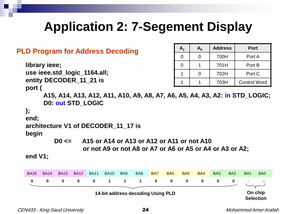
Application 2: 7-Segement Display
library ieee;
use ieee.std_logic_1164.all;
entity DECODER_11_21 is
port (
A15, A14, A13, A12, A11, A10, A9, A8, A7, A6, A5, A4, A3, A2: in STD_LOGIC;
D0: out STD_LOGIC
);
end;
architecture V1 of DECODER_11_17 is
begin
D0 <= A15 or A14 or A13 or A12 or A11 or not A10
or not A9 or not A8 or A7 or A6 or A5 or A4 or A3 or A2;
end V1;
BA15 BA14 BA13 BA12 BA11 BA10 BA9 BA8 BA7 BA6 BA5 BA4 BA3 BA2 BA1 BA0
0 0 0 0 0 1 1 1 0 0 0 0 0 0 - -
On chip
Selection
PLD Program for Address DecodingA1 A0 Address Port
0 0 700H Port A
0 1 701H Port B
1 0 702H Port C
1 1 703H Control Word
14-bit address decoding Using PLD
Mohammed Amer Arafah25CEN433 - King Saud University
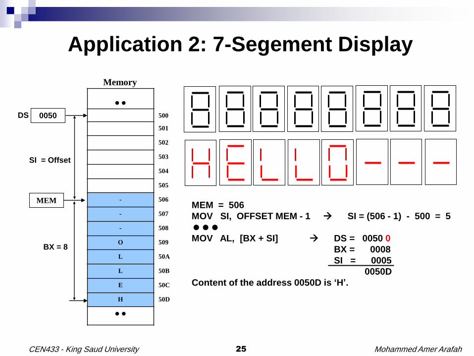
Application 2: 7-Segement Display
MEM
SI = Offset
BX = 8
Memory
DS 0050
MEM = 506
MOV SI, OFFSET MEM - 1 SI = (506 - 1) - 500 = 5
MOV AL, [BX + SI] DS = 0050 0
BX = 0008
SI = 0005
0050D
Content of the address 0050D is ‘H’.
500
501
502
503
504
505
- 506
- 507
- 508
O 509
L 50A
L 50B
E 50C
H 50D
Mohammed Amer Arafah26CEN433 - King Saud University
Application 2: 7-Segement Display
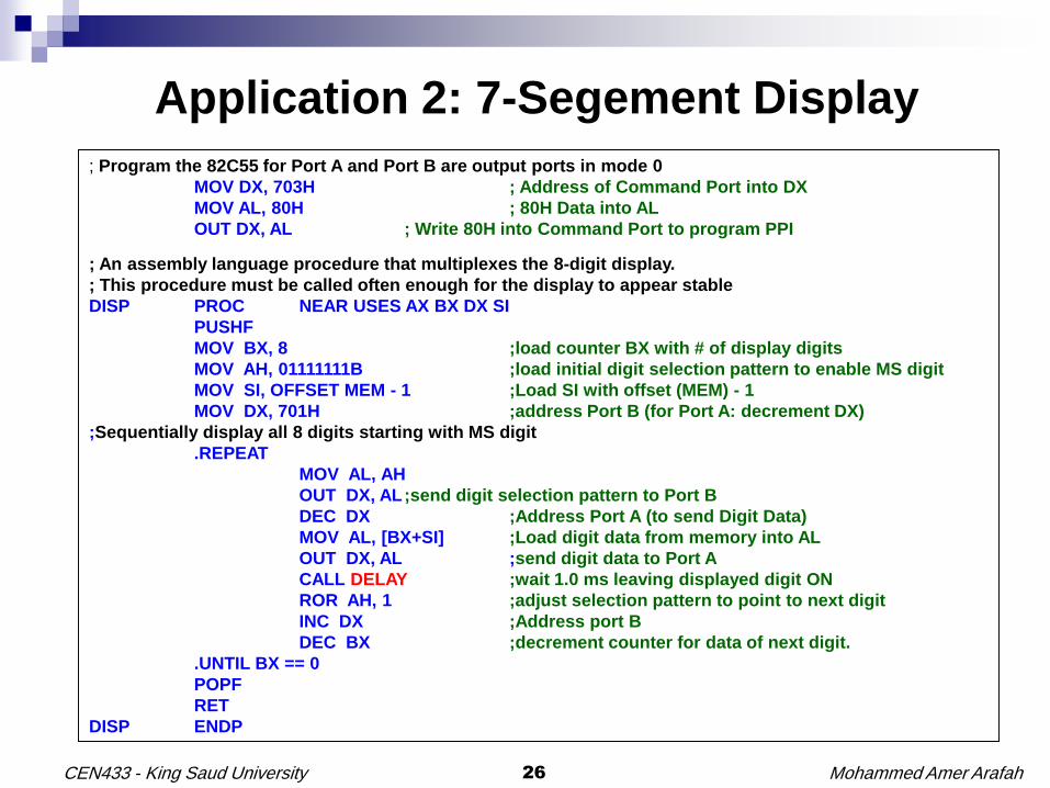
; Program the 82C55 for Port A and Port B are output ports in mode 0
MOV DX, 703H ; Address of Command Port into DX
MOV AL, 80H ; 80H Data into AL
OUT DX, AL ; Write 80H into Command Port to program PPI
; An assembly language procedure that multiplexes the 8-digit display.
; This procedure must be called often enough for the display to appear stable
DISP PROC NEAR USES AX BX DX SI
PUSHF
MOV BX, 8 ;load counter BX with # of display digits
MOV AH, 01111111B ;load initial digit selection pattern to enable MS digit
MOV SI, OFFSET MEM - 1 ;Load SI with offset (MEM) - 1
MOV DX, 701H ;address Port B (for Port A: decrement DX)
;Sequentially display all 8 digits starting with MS digit
.REPEAT
MOV AL, AH
OUT DX, AL;send digit selection pattern to Port B
DEC DX ;Address Port A (to send Digit Data)
MOV AL, [BX+SI] ;Load digit data from memory into AL
OUT DX, AL ;send digit data to Port A
CALL DELAY ;wait 1.0 ms leaving displayed digit ON
ROR AH, 1 ;adjust selection pattern to point to next digit
INC DX ;Address port B
DEC BX ;decrement counter for data of next digit.
.UNTIL BX == 0
POPF
RET
DISP ENDP
Mohammed Amer Arafah27CEN433 - King Saud University
Application 2: 7-Segement Display
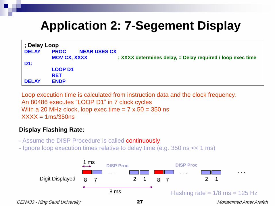
; Delay LoopDELAY PROC NEAR USES CX
MOV CX, XXXX ; XXXX determines delay, = Delay required / loop exec time
D1:
LOOP D1
RET
DELAY ENDP
Loop execution time is calculated from instruction data and the clock frequency.
An 80486 executes “LOOP D1” in 7 clock cycles
With a 20 MHz clock, loop exec time = 7 x 50 = 350 ns
XXXX = 1ms/350ns
Display Flashing Rate:
- Assume the DISP Procedure is called continuously
- Ignore loop execution times relative to delay time (e.g. 350 ns << 1 ms)
. . .
Digit Displayed 8 7 2 1
. . .
7 2 18
1 ms
8 ms
. . .
Flashing rate = 1/8 ms = 125 Hz
DISP Proc DISP Proc
Mohammed Amer Arafah28CEN433 - King Saud University
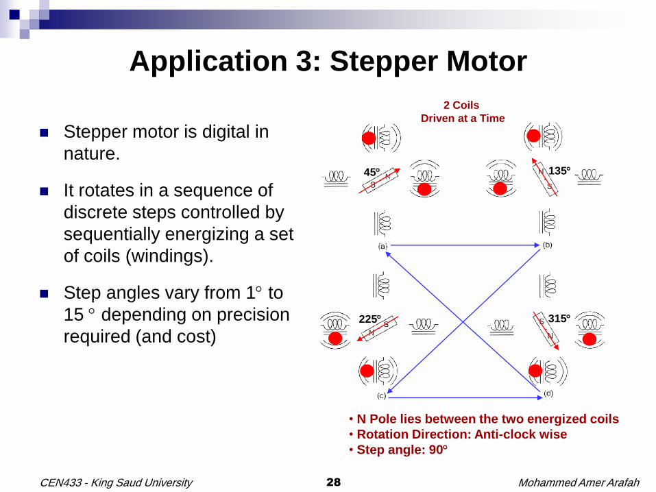
Application 3: Stepper Motor
Stepper motor is digital in
nature.
It rotates in a sequence of
discrete steps controlled by
sequentially energizing a set
of coils (windings).
Step angles vary from 1 to
15 depending on precision
required (and cost)
• N Pole lies between the two energized coils
• Rotation Direction: Anti-clock wise
• Step angle: 90
45 135
315
2 Coils
Driven at a Time
225
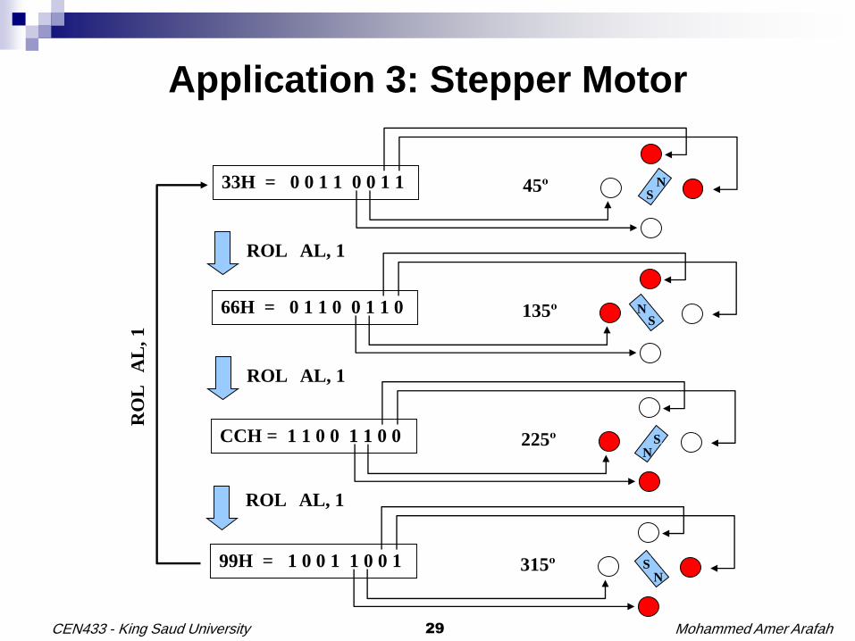
Mohammed Amer Arafah29CEN433 - King Saud University
Application 3: Stepper Motor
33H = 0 0 1 1 0 0 1 1S
N45º
ROL AL, 1
CCH = 1 1 0 0 1 1 0 0 SN
225º
ROL AL, 1
99H = 1 0 0 1 1 0 0 1 SN
315º
ROL AL, 1
66H = 0 1 1 0 0 1 1 0 N135ºS
RO
L
AL
, 1
Mohammed Amer Arafah30CEN433 - King Saud University
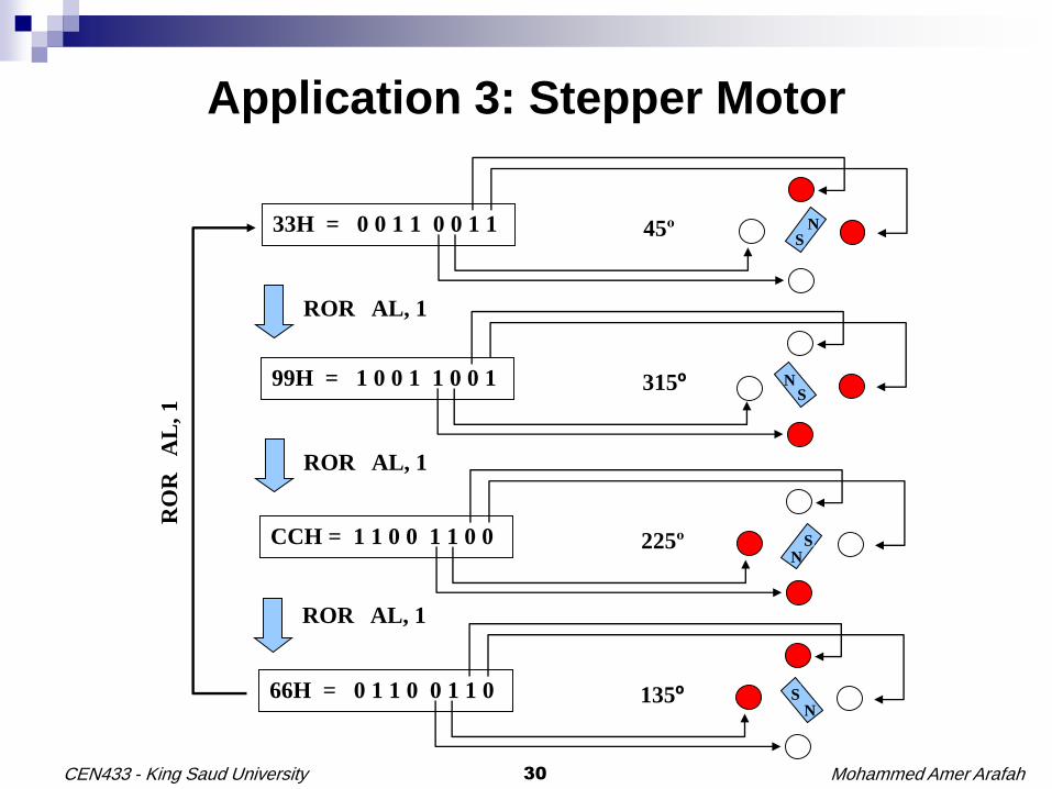
Application 3: Stepper Motor
33H = 0 0 1 1 0 0 1 1S
N45º
ROR AL, 1
CCH = 1 1 0 0 1 1 0 0 SN
225º
ROR AL, 1
66H = 0 1 1 0 0 1 1 0 SN
135º
ROR AL, 1
99H = 1 0 0 1 1 0 0 1 N315ºS
RO
R
AL
, 1
Mohammed Amer Arafah31CEN433 - King Saud University
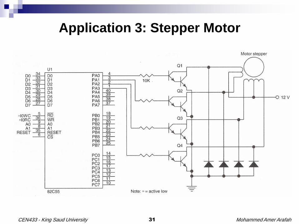
Application 3: Stepper Motor
Mohammed Amer Arafah32CEN433 - King Saud University
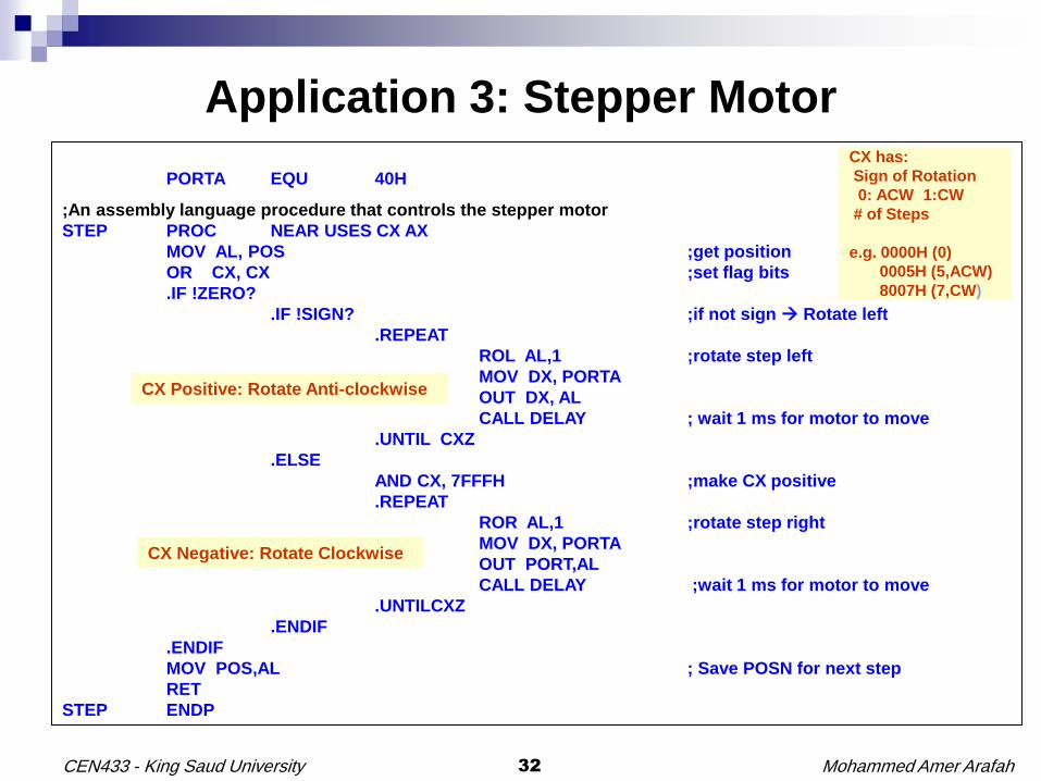
Application 3: Stepper Motor
PORTA EQU 40H
;An assembly language procedure that controls the stepper motor
STEP PROC NEAR USES CX AX
MOV AL, POS ;get position
OR CX, CX ;set flag bits
.IF !ZERO?
.IF !SIGN? ;if not sign Rotate left
.REPEAT
ROL AL,1 ;rotate step left
MOV DX, PORTA
OUT DX, AL
CALL DELAY ; wait 1 ms for motor to move
.UNTIL CXZ
.ELSE
AND CX, 7FFFH ;make CX positive
.REPEAT
ROR AL,1 ;rotate step right
MOV DX, PORTA
OUT PORT,AL
CALL DELAY ;wait 1 ms for motor to move
.UNTILCXZ
.ENDIF
.ENDIF
MOV POS,AL ; Save POSN for next step
RET
STEP ENDP
CX Positive: Rotate Anti-clockwise
CX Negative: Rotate Clockwise
CX has:
Sign of Rotation
0: ACW 1:CW
# of Steps
e.g. 0000H (0)
0005H (5,ACW)
8007H (7,CW)
Mohammed Amer Arafah33CEN433 - King Saud University
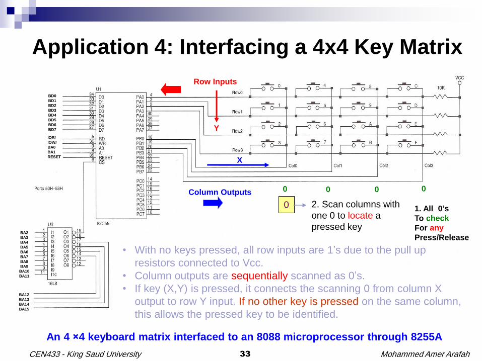
Application 4: Interfacing a 4x4 Key Matrix
An 4 ×4 keyboard matrix interfaced to an 8088 microprocessor through 8255A
BD0
BD1
BD2
BD3
BD4
BD5
BD6
BD7
IOR/
IOW/
BA0
BA1
RESET
BA2
BA3
BA4
BA5
BA6
BA7
BA8
BA9
BA10
BA11
BA12
BA13
BA14
BA15
Row Inputs
Column Outputs
• With no keys pressed, all row inputs are 1’s due to the pull up
resistors connected to Vcc.
• Column outputs are sequentially scanned as 0’s.
• If key (X,Y) is pressed, it connects the scanning 0 from column X
output to row Y input. If no other key is pressed on the same column,
this allows the pressed key to be identified.
X
Y
0 2. Scan columns with
one 0 to locate a
pressed key
1. All 0’s
To check
For any
Press/Release
0 0 0 0
Mohammed Amer Arafah34CEN433 - King Saud University
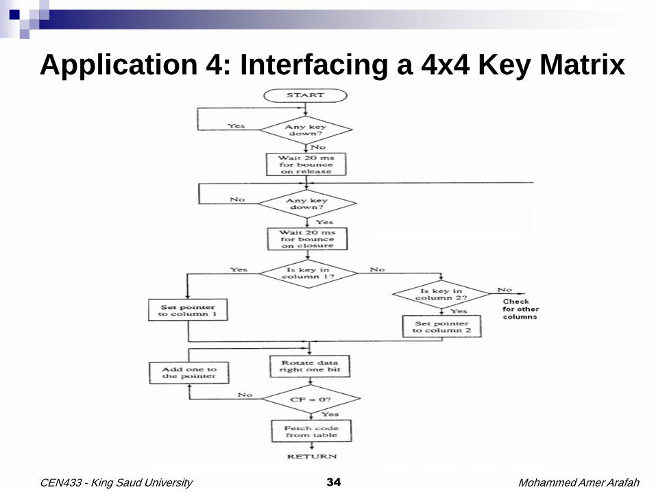
Application 4: Interfacing a 4x4 Key Matrix
Mohammed Amer Arafah35CEN433 - King Saud University
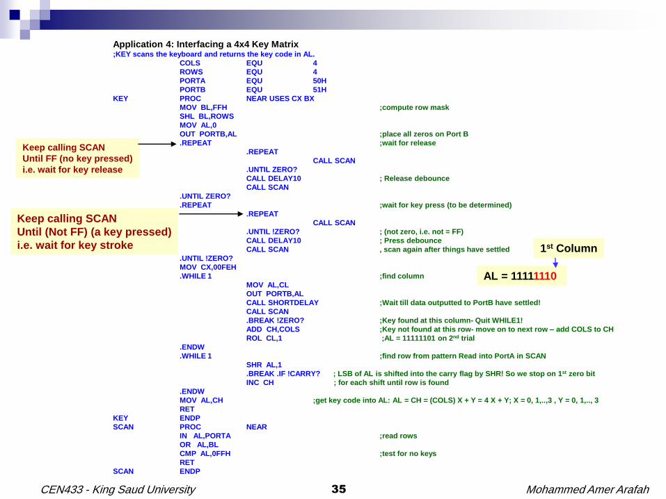
Application 4: Interfacing a 4x4 Key Matrix;KEY scans the keyboard and returns the key code in AL.
COLS EQU 4
ROWS EQU 4
PORTA EQU 50H
PORTB EQU 51H
KEY PROC NEAR USES CX BX
MOV BL,FFH ;compute row mask
SHL BL,ROWS
MOV AL,0
OUT PORTB,AL ;place all zeros on Port B
.REPEAT ;wait for release
.REPEAT
CALL SCAN
.UNTIL ZERO?
CALL DELAY10 ; Release debounce
CALL SCAN
.UNTIL ZERO?
.REPEAT ;wait for key press (to be determined)
.REPEAT
CALL SCAN
.UNTIL !ZERO? ; (not zero, i.e. not = FF)
CALL DELAY10 ; Press debounce
CALL SCAN , scan again after things have settled
.UNTIL !ZERO?
MOV CX,00FEH
.WHILE 1 ;find column
MOV AL,CL
OUT PORTB,AL
CALL SHORTDELAY ;Wait till data outputted to PortB have settled!
CALL SCAN
.BREAK !ZERO? ;Key found at this column- Quit WHILE1!
ADD CH,COLS ;Key not found at this row- move on to next row – add COLS to CH
ROL CL,1 ;AL = 11111101 on 2nd trial
.ENDW
.WHILE 1 ;find row from pattern Read into PortA in SCAN
SHR AL,1
.BREAK .IF !CARRY? ; LSB of AL is shifted into the carry flag by SHR! So we stop on 1st zero bit
INC CH ; for each shift until row is found
.ENDW
MOV AL,CH ;get key code into AL: AL = CH = (COLS) X + Y = 4 X + Y; X = 0, 1,..,3 , Y = 0, 1,.., 3
RET
KEY ENDP
SCAN PROC NEAR
IN AL,PORTA ;read rows
OR AL,BL
CMP AL,0FFH ;test for no keys
RET
SCAN ENDP
Keep calling SCAN
Until FF (no key pressed)
i.e. wait for key release
Keep calling SCAN
Until (Not FF) (a key pressed)
i.e. wait for key stroke
AL = 11111110
1st Column
Mohammed Amer Arafah36CEN433 - King Saud University
Mode 1 (Strobed Input/Output)
This functional configuration provides a means fortransferring I/O data to or from a specified port in conjunctionwith strobes or “hand shaking” signals. In mode 1, port A andport B use the lines on port C to generate or accept these“hand shaking” signals.
Mode 1 Basic Function Definitions:
Two Groups (Group A and Group B).
Each group contains one 8-bit port and one 5-bit (Group A) or 3-bit (Group B) control/data port.
The 8-bit data port can be either input or output. Both inputs and outputs are latched.
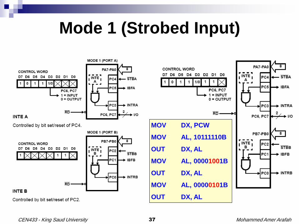
Mohammed Amer Arafah37CEN433 - King Saud University
Mode 1 (Strobed Input)
MOV DX, PCW
MOV AL, 10111110B
OUT DX, AL
MOV AL, 00001001B
OUT DX, AL
MOV AL, 00000101B
OUT DX, AL
Mohammed Amer Arafah38CEN433 - King Saud University
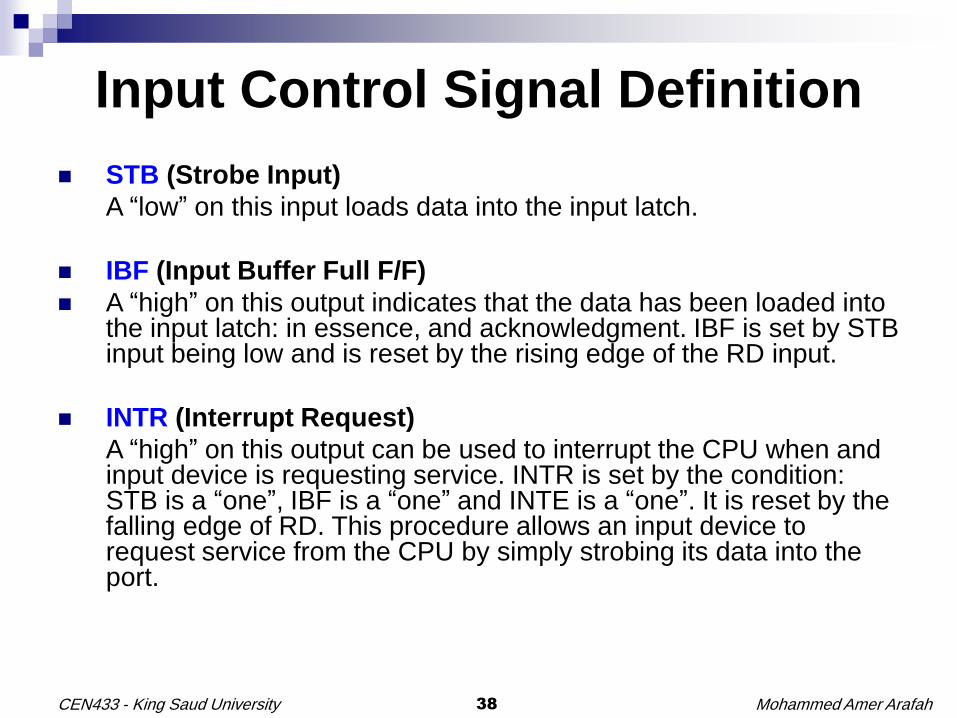
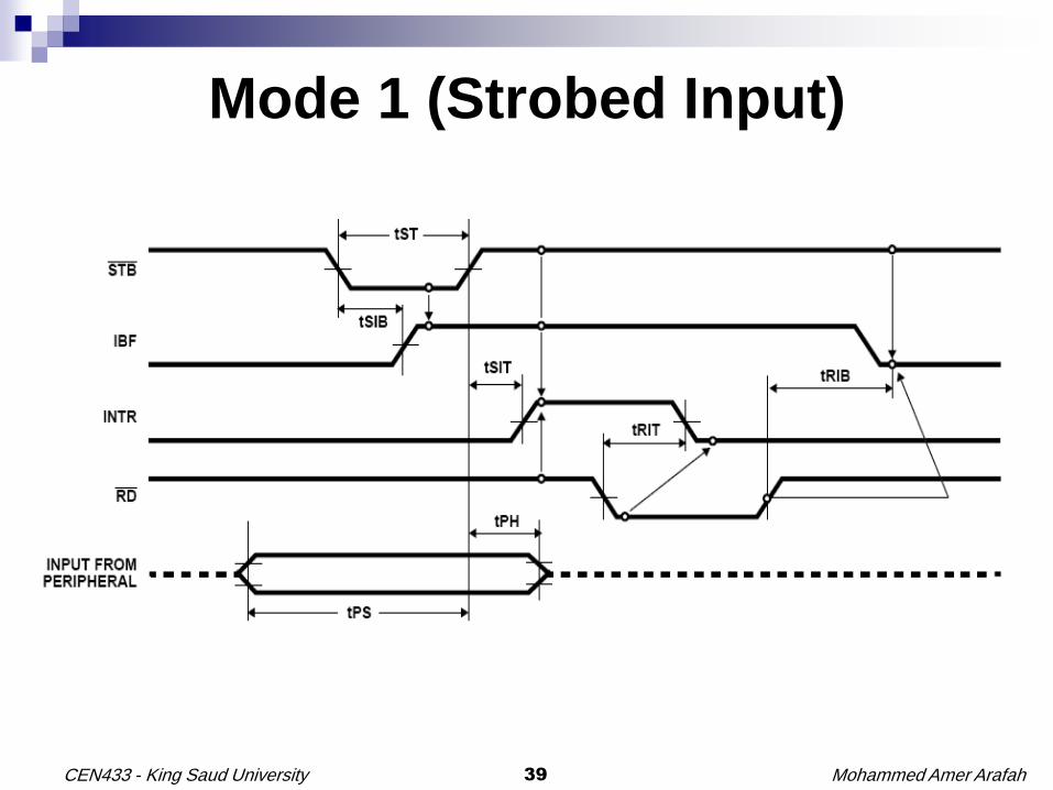
Input Control Signal Definition
STB (Strobe Input)
A “low” on this input loads data into the input latch.
IBF (Input Buffer Full F/F)
A “high” on this output indicates that the data has been loaded into the input latch: in essence, and acknowledgment. IBF is set by STB input being low and is reset by the rising edge of the RD input.
INTR (Interrupt Request)
A “high” on this output can be used to interrupt the CPU when and input device is requesting service. INTR is set by the condition: STB is a “one”, IBF is a “one” and INTE is a “one”. It is reset by the falling edge of RD. This procedure allows an input device to request service from the CPU by simply strobing its data into the port.
Mohammed Amer Arafah39CEN433 - King Saud University
Mode 1 (Strobed Input)
Mohammed Amer Arafah40CEN433 - King Saud University
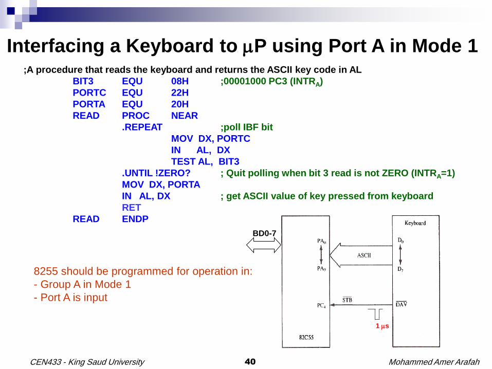
;A procedure that reads the keyboard and returns the ASCII key code in AL
BIT3 EQU 08H ;00001000 PC3 (INTRA)
PORTC EQU 22H
PORTA EQU 20H
READ PROC NEAR
.REPEAT ;poll IBF bit
MOV DX, PORTC
IN AL, DX
TEST AL, BIT3
.UNTIL !ZERO? ; Quit polling when bit 3 read is not ZERO (INTRA=1)
MOV DX, PORTA
IN AL, DX ; get ASCII value of key pressed from keyboard
RET
READ ENDP
Interfacing a Keyboard to mP using Port A in Mode 1
8255 should be programmed for operation in:
- Group A in Mode 1
- Port A is input
1 ms
BD0-7
Mohammed Amer Arafah41CEN433 - King Saud University
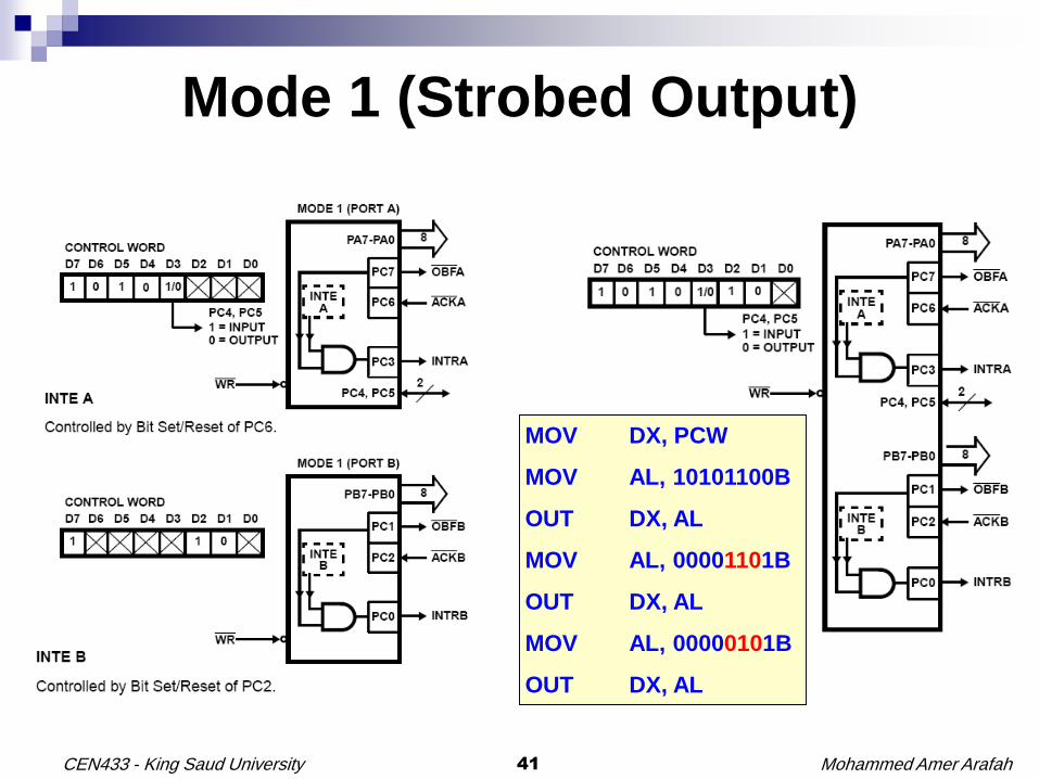
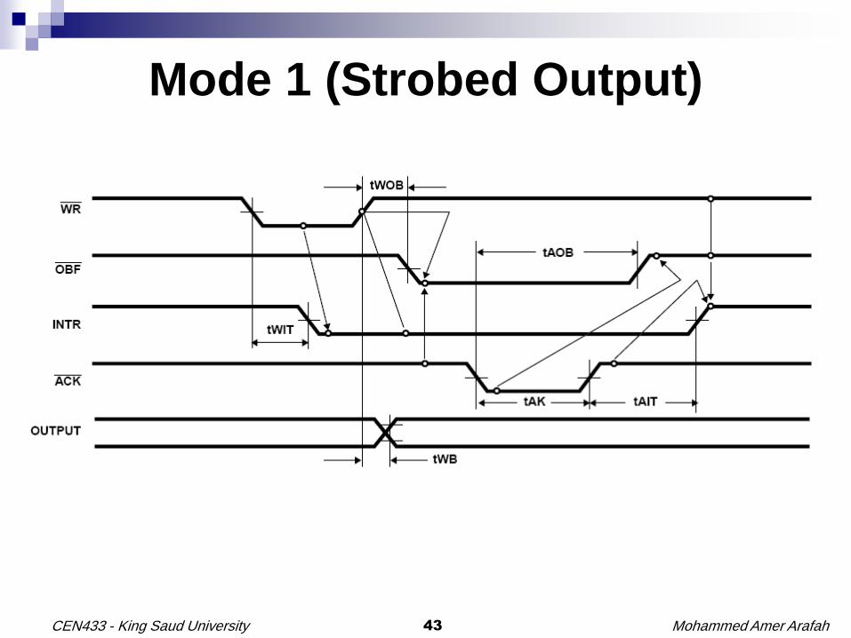
Mode 1 (Strobed Output)
MOV DX, PCW
MOV AL, 10101100B
OUT DX, AL
MOV AL, 00001101B
OUT DX, AL
MOV AL, 00000101B
OUT DX, AL
Mohammed Amer Arafah42CEN433 - King Saud University
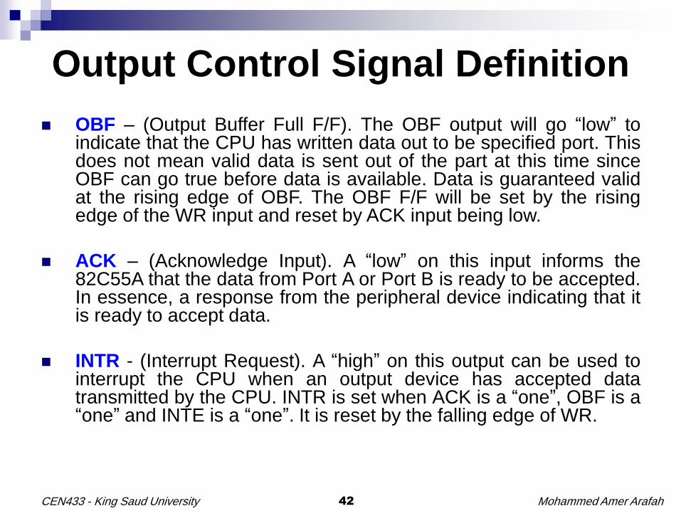
Output Control Signal Definition
OBF – (Output Buffer Full F/F). The OBF output will go “low” toindicate that the CPU has written data out to be specified port. Thisdoes not mean valid data is sent out of the part at this time sinceOBF can go true before data is available. Data is guaranteed validat the rising edge of OBF. The OBF F/F will be set by the risingedge of the WR input and reset by ACK input being low.
ACK – (Acknowledge Input). A “low” on this input informs the82C55A that the data from Port A or Port B is ready to be accepted.In essence, a response from the peripheral device indicating that itis ready to accept data.
INTR - (Interrupt Request). A “high” on this output can be used tointerrupt the CPU when an output device has accepted datatransmitted by the CPU. INTR is set when ACK is a “one”, OBF is a“one” and INTE is a “one”. It is reset by the falling edge of WR.
Mohammed Amer Arafah43CEN433 - King Saud University
Mode 1 (Strobed Output)
Mohammed Amer Arafah44CEN433 - King Saud University
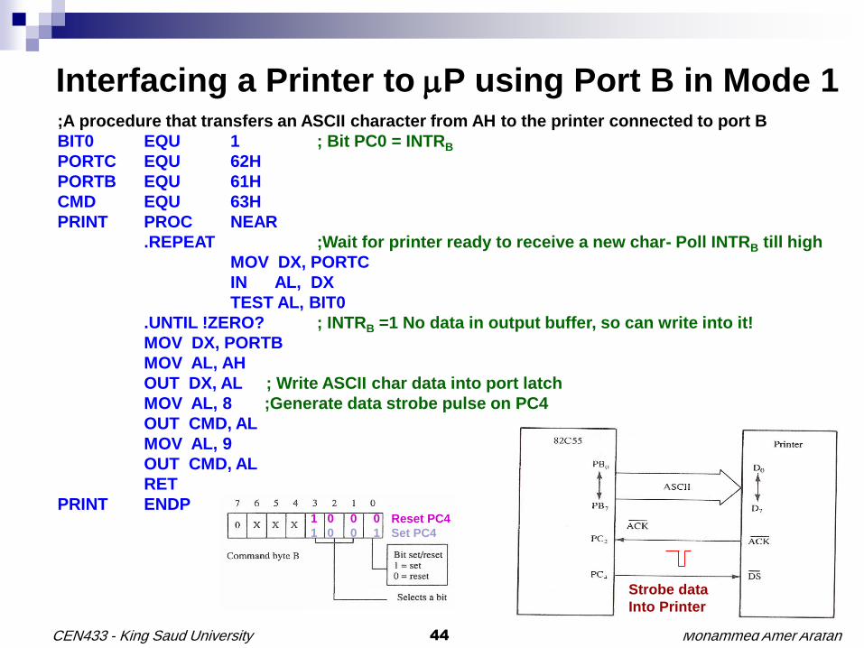
Interfacing a Printer to mP using Port B in Mode 1;A procedure that transfers an ASCII character from AH to the printer connected to port B
BIT0 EQU 1 ; Bit PC0 = INTRB
PORTC EQU 62H
PORTB EQU 61H
CMD EQU 63H
PRINT PROC NEAR
.REPEAT ;Wait for printer ready to receive a new char- Poll INTRB till high
MOV DX, PORTC
IN AL, DX
TEST AL, BIT0
.UNTIL !ZERO? ; INTRB =1 No data in output buffer, so can write into it!
MOV DX, PORTB
MOV AL, AH
OUT DX, AL ; Write ASCII char data into port latch
MOV AL, 8 ;Generate data strobe pulse on PC4
OUT CMD, AL
MOV AL, 9
OUT CMD, AL
RET
PRINT ENDP1 0 0 0
1 0 0 1
Reset PC4
Set PC4
Strobe data
Into Printer
Mohammed Amer Arafah45CEN433 - King Saud University
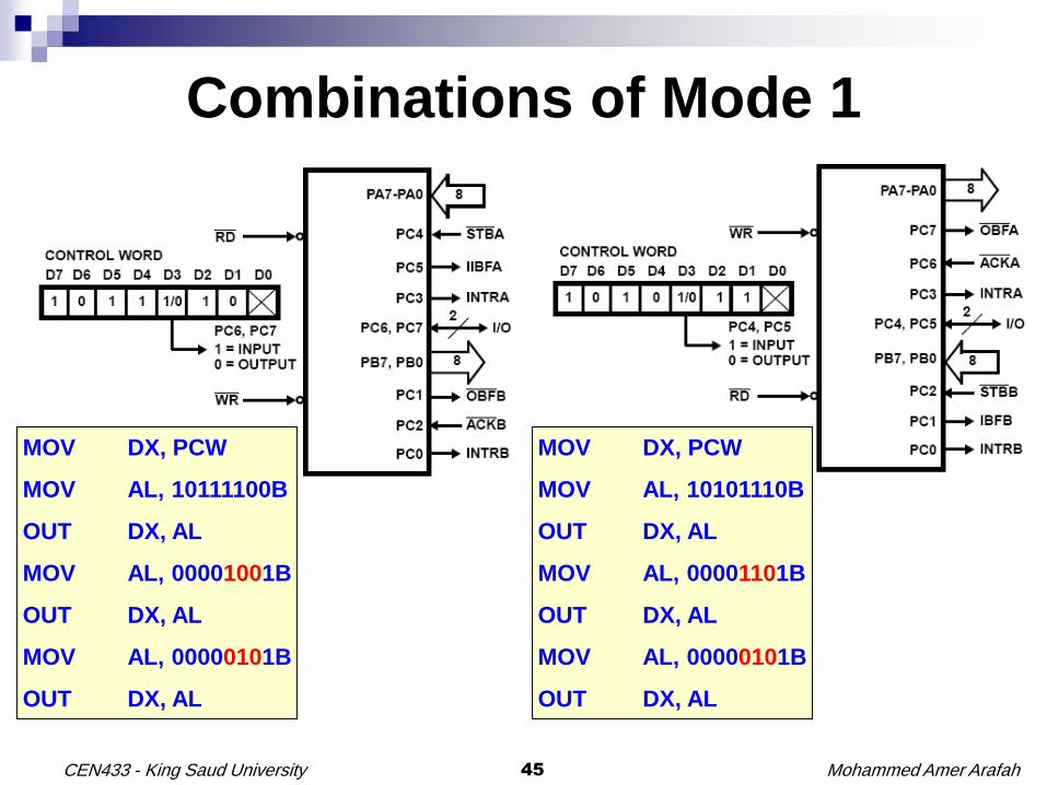
Combinations of Mode 1
MOV DX, PCW
MOV AL, 10101110B
OUT DX, AL
MOV AL, 00001101B
OUT DX, AL
MOV AL, 00000101B
OUT DX, AL
MOV DX, PCW
MOV AL, 10111100B
OUT DX, AL
MOV AL, 00001001B
OUT DX, AL
MOV AL, 00000101B
OUT DX, AL
Mohammed Amer Arafah46CEN433 - King Saud University
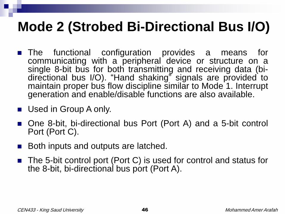
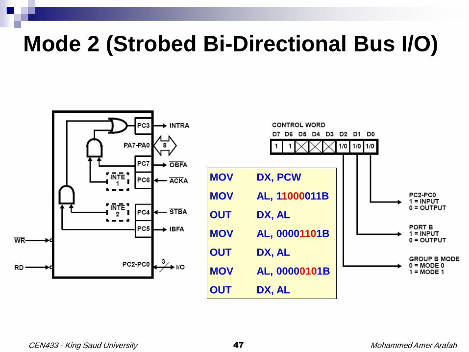
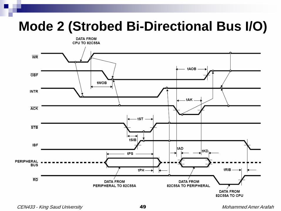
Mode 2 (Strobed Bi-Directional Bus I/O)
The functional configuration provides a means forcommunicating with a peripheral device or structure on asingle 8-bit bus for both transmitting and receiving data (bi-directional bus I/O). “Hand shaking” signals are provided tomaintain proper bus flow discipline similar to Mode 1. Interruptgeneration and enable/disable functions are also available.
Used in Group A only.
One 8-bit, bi-directional bus Port (Port A) and a 5-bit controlPort (Port C).
Both inputs and outputs are latched.
The 5-bit control port (Port C) is used for control and status forthe 8-bit, bi-directional bus port (Port A).
Mohammed Amer Arafah47CEN433 - King Saud University
Mode 2 (Strobed Bi-Directional Bus I/O)
MOV DX, PCW
MOV AL, 11000011B
OUT DX, AL
MOV AL, 00001101B
OUT DX, AL
MOV AL, 00000101B
OUT DX, AL
Mohammed Amer Arafah48CEN433 - King Saud University
Bi-Directional Bus I/O Control Signal Definition
INTR - (Interrupt Request). A high on this output can be used to interrupt the CPU for both input or output operations.
Output Operations:
OBF - (Output Buffer Full). The OBF output will go “low” to indicate that the CPU has written data out to port A.
ACK - (Acknowledge). A “low” on this input enables the three-state output buffer of port A to send out the data. Otherwise, the output buffer will be in the high impedance state.
INTE 1 - (The INTE flip-flop associated with OBF). Controlled by bit set/reset of PC4.
Input Operations
STB - (Strobe Input). A “low” on this input loads data into the input latch.
IBF - (Input Buffer Full F/F). A “high” on this output indicates that data has been loaded into the input latch.
INTE 2 - (The INTE flip-flop associated with IBF). Controlled by bit set/reset of PC4.
Mohammed Amer Arafah49CEN433 - King Saud University
Mode 2 (Strobed Bi-Directional Bus I/O)
Mohammed Amer Arafah50CEN433 - King Saud University
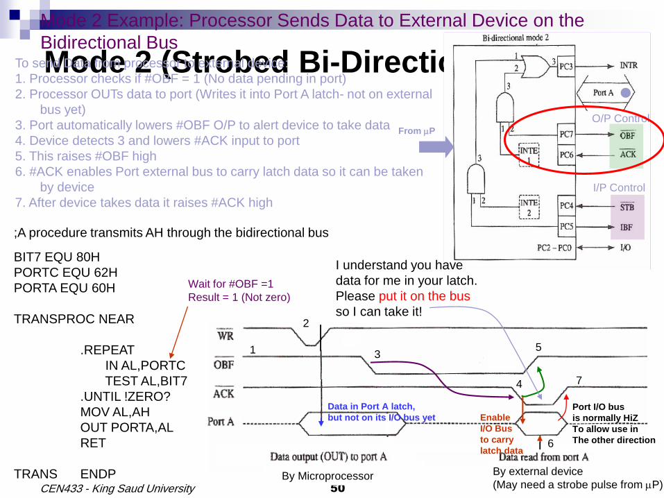
Mode 2 (Strobed Bi-Directional Bus I/O)
Mode 2 Example: Processor Sends Data to External Device on the
Bidirectional BusTo send Data from processor to external device:
1. Processor checks if #OBF = 1 (No data pending in port)
2. Processor OUTs data to port (Writes it into Port A latch- not on external
bus yet)
3. Port automatically lowers #OBF O/P to alert device to take data
4. Device detects 3 and lowers #ACK input to port
5. This raises #OBF high
6. #ACK enables Port external bus to carry latch data so it can be taken
by device
7. After device takes data it raises #ACK high
I/P Control
O/P ControlFrom mP
I understand you have
data for me in your latch.
Please put it on the bus
so I can take it!
By external device
(May need a strobe pulse from mP)By Microprocessor
Data in Port A latch,
but not on its I/O bus yetPort I/O bus
is normally HiZ
To allow use in
The other direction
Enable
I/O Bus
to carry
latch data
1
2
3
4
6
5
7
;A procedure transmits AH through the bidirectional bus
BIT7 EQU 80H
PORTC EQU 62H
PORTA EQU 60H
TRANSPROC NEAR
.REPEAT
IN AL,PORTC
TEST AL,BIT7
.UNTIL !ZERO?
MOV AL,AH
OUT PORTA,AL
RET
TRANS ENDP
Wait for #OBF =1
Result = 1 (Not zero)
Mohammed Amer Arafah51CEN433 - King Saud University
Mode 2 (Strobed Bi-Directional Bus I/O)
Mode 2 Example: Processor Receives Data from External Device on
the Bidirectional Bus
To Receive Data:
1. External device sending data checks if #IBF = 0 (No pending
data in port latch not read by processor) (Hardware Polling)
2. Then it puts its data on external bus and strobes it into port latch
using #STB
3. IBF automatically goes high until data is read by processor
4. Processor polls IBF for IBF = 1 to make sure data is in port latch
(software polling)
5. Processor reads data from port
6. This automatically lowers IBF to enable further writes
I/P Control
O/P Control
By device on the other side
HiZ external
bus!
(It is OK…
processor
reads
its data bus)
To mP
By Microprocessor
latch
Port I/O bus
is normally HiZ
Hardware Polling for IBF = 0 by device to generate #STB
To avoid overwriting existing data in Port not read by processor yet
;A procedure that reads data from the bidirectional bus into AL
BIT5 EQU 20H
PORTC EQU 62H
PORTA EQU 60H
READ PROC NEAR
.REPEAT ;Wait for IBF = 1
IN AL,PORTC
TEST AL,BIT5
.UNTIL !ZERO?
IN AL,PORTA
RET
READ PROC NEAR
1
2
3 4
5
Step 4
6
2
Step 5
Mohammed Amer Arafah52CEN433 - King Saud University
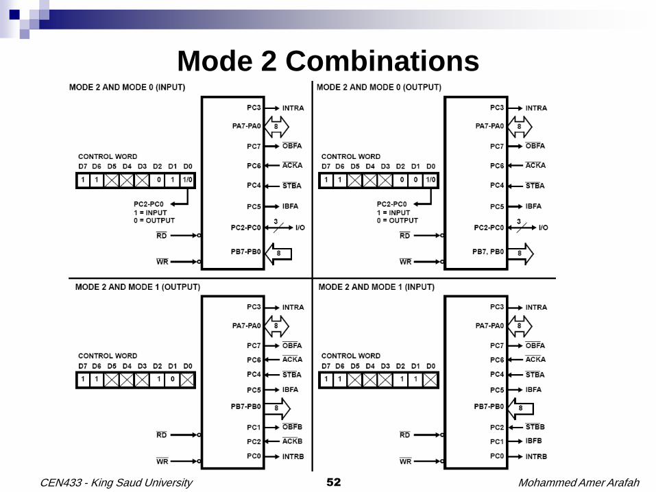
Mode 2 Combinations
Mohammed Amer Arafah53CEN433 - King Saud University
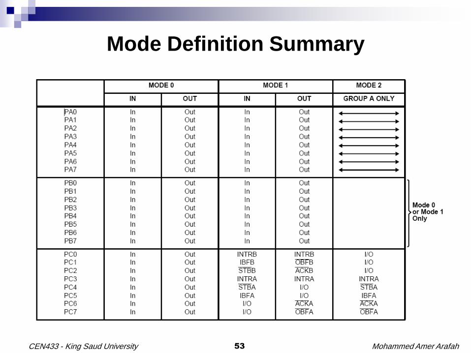
Mode Definition Summary
Mohammed Amer Arafah54CEN433 - King Saud University
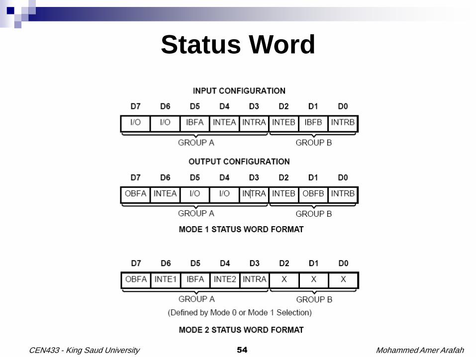
Status Word
Mohammed Amer Arafah55CEN433 - King Saud University
Mohammed Amer Arafah56CEN433 - King Saud University
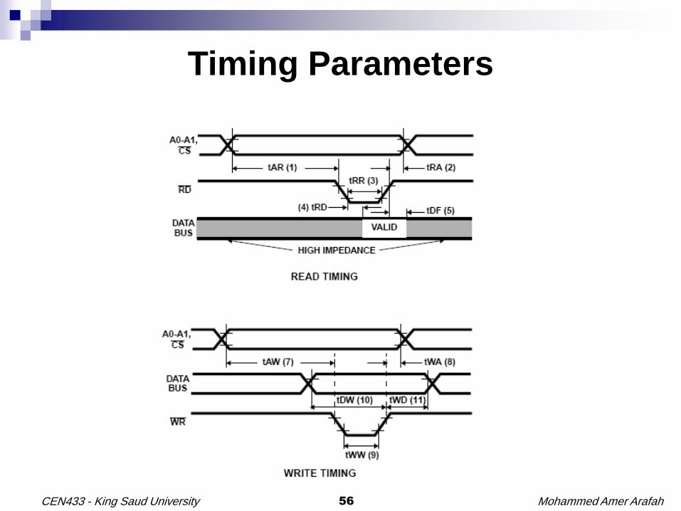
Timing Parameters
Mohammed Amer Arafah57CEN433 - King Saud University
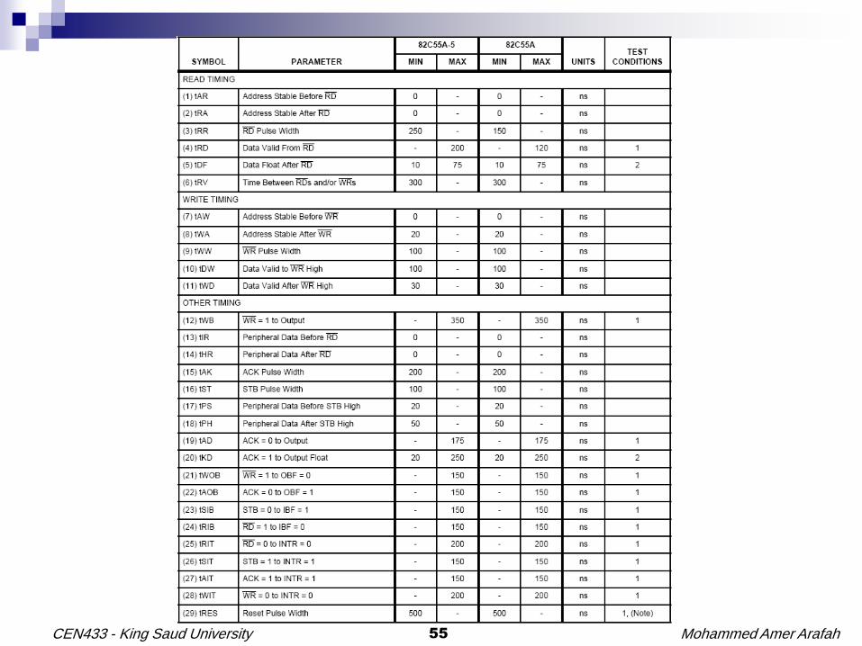
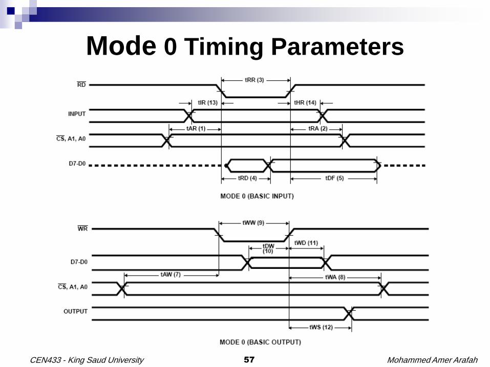
Mode 0 Timing Parameters
Mohammed Amer Arafah58CEN433 - King Saud University
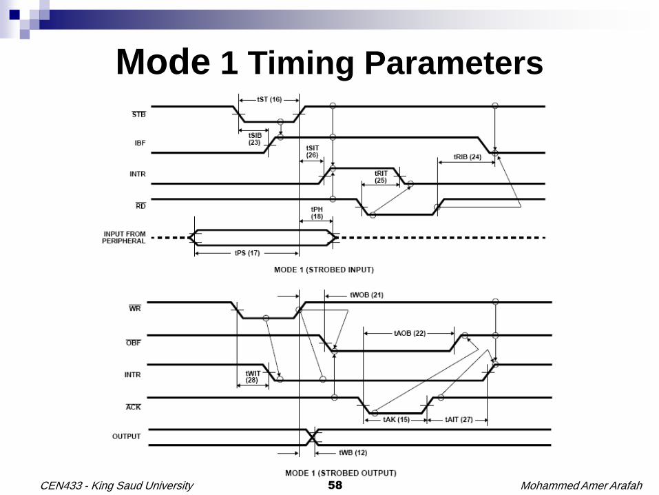
Mode 1 Timing Parameters
Mohammed Amer Arafah59CEN433 - King Saud University
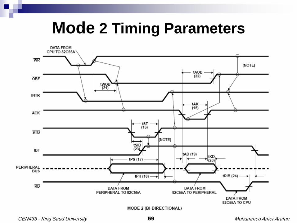
Mode 2 Timing Parameters